1
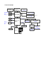
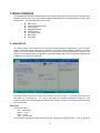
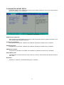
AR-B5070
ISA-Bus SBC with
Pentium-M or Celeron-M CPU
User Guide
Edition: 1.1
Book Number: AR-B5070 11.28.07
Table of Contents
0. PREFACE.....................................................................................................................................................................3
0.1 COPYRIGHT NOTICE AND DISCLAIMER .....................................................................................................................................3
0.2 WELCOME TO THE AR-B5070 CPU BOARD................................................................................................................................3
0.3 BEFORE YOU USE THIS GUIDE ...................................................................................................................................................3
0.4 RETURNING YOUR BOARD FOR SERVICE.................................................................................................................................3
0.5 TECHNICAL SUPPORT AND USER COMMENTS ........................................................................................................................3
0.6 STATIC ELECTRICITY PRECAUTIONS ........................................................................................................................................4
1. INTRODUCTION ..........................................................................................................................................................5
1.1 PACKING LIST................................................................................................................................................................................5
1.2 SPECIFICATIONS...........................................................................................................................................................................6
1.3 BLOCK DIAGRAM...........................................................................................................................................................................8
2. INSTALLATION ............................................................................................................................................................9
2.1 AR-B5070'S BOARD DIMENSIONS ...............................................................................................................................................9
3. CONNECTION ...........................................................................................................................................................10
3.1 VGA CONNECTOR ( VGA1) .......................................................................................................................................................10
3.2 VOLTAGE SOUCE FOR LCD INVERTER (LCDPW1) .................................................................................................................10
3.3 LCD CONNECTOR (LCD).............................................................................................................................................................10
3.4 HARD DISK CONNECTOR (IDE1) ...............................................................................................................................................11
3.5 COMPACT FLASH SLOT (CFD1).................................................................................................................................................11
3.6 SERIAL PORT (COM1) .................................................................................................................................................................12
3.7 SERIAL PORT (COM2) .................................................................................................................................................................12
3.8 PC104 ..........................................................................................................................................................................................12
3.9 AUDIO CONNECTOR (AUDIO1) ..................................................................................................................................................12
3.10 USB CONNECTOR (USB1) ........................................................................................................................................................12
3.11 ATX POWER CONNECTOR........................................................................................................................................................12
3.12 FLOPPY DISK DRIVE CONNECTOR (FDD1)) ........................................................................................................................13
3.13 PARALLEL PORT CONNECTOR (LPT1) ...................................................................................................................................13
3.14 KEYBOARD/MOUSE CONNECTOR (PS1) ................................................................................................................................14
3.15 KEYBOARD/MOUSE CONNECTOR (KB1) ................................................................................................................................14
3.16 CPU FAN CONNECTOR(CPUF1) ..............................................................................................................................................14
3.17 RJ45 CONNECTOR (LAN1)........................................................................................................................................................14
3.18 POWER INPUT CONNECTOR (PWR1))..................................................................................................................................15
3.19 GPIO CONNECTOR (GPIO1) .....................................................................................................................................................15
3.20 CMOS CLEAR (JP1) AND CMOS BAT (BAT1) ..........................................................................................................................15
3.21 COM2 FUNCTION FOR RS232 (COM2) ....................................................................................................................................15
3.22 LCD VOLTAGE SELECT (JP1)...................................................................................................................................................15
3.23 HARDWARE RESET PIN (JP3) ..................................................................................................................................................15
3.24 CPU TYPE SELECT (J1) ............................................................................................................................................................15
3.25 POWER BUTTON (PWR_BTN) ..................................................................................................................................................16
3.26 SRAM BATTERY CONNECTOR (BAT2) ..................................................................................................................................16
3.27 SRAM IO DEFINE SELECT (JP2, JP3))...................................................................................................................................16
3.28 COM2 RS422/RS485 SELECT(JRS1) ........................................................................................................................................16
3.29 COM2 FUNCTION FOR RS422/RS485 (JCOM2) ......................................................................................................................16
4. WATCHDOG TIMER CONFIGURATION ...................................................................................................................17
4.1 WATCHDOG TIMER SETTING ....................................................................................................................................................17
5. BIOS CONSOLE ........................................................................................................................................................19
5.1 MAIN SETUP.................................................................................................................................................................................19
5.2 ADVANCED CHIPSET SETUP .....................................................................................................................................................21
5.3 POWER SETUP ............................................................................................................................................................................22
5.4 PERIPHERALS SETUP ................................................................................................................................................................22
5.5 PNP/PCI SETUP ...........................................................................................................................................................................23
5.6 PC HEALTH SETUP .....................................................................................................................................................................24
5.7 BOOT SETUP ...............................................................................................................................................................................24
5.8 EXIT SETUP..................................................................................................................................................................................25
5.9 BIOS UPDATE ..............................................................................................................................................................................26
APPENDIX A. ADDRESS MAPPING .............................................................................................................................27
IO ADDRESS MAP..............................................................................................................................................................................27
APPENDIX B. INTERRUPT REQUEST (IRQ)................................................................................................................28
2
0. PREFACE
0.1 COPYRIGHT NOTICE AND DISCLAIMER
This document is copyrighted, 2007, by Acrosser Technology Co., Ltd. All rights are reserved. No part
of this manual may be reproduced, copied, transcribed, stored in a retrieval system, or translated into
any language or computer language in any form or by any means, such as electronic, mechanical,
magnetic, optical, chemical, manual or other means without the prior written permission or original
manufacturer.
Acrosser Technology assumes no responsibility or warranty with respect to the content in this manual
and specifically disclaims any implied warranty of merchantability or fitness for any particular purpose.
Furthermore, Acrosser Technology reserves the right to make improvements to the products described
in this manual at any times without notice. Such revisions will be posted on the Internet
(WWW.ACROSSER.COM) as soon as possible.
Possession, use, or copy of the software described in this publication is authorized only pursuant to
valid written license from Acrosser or an authorized sub licensor.
ACKNOWLEDGEMENTS
Acrosser, AMI, IBM PC/AT, ALI, Windows 3.1, MS-DOS…are registered trademarks.
All other trademarks and registered trademarks are the property of their respective owners.
0.2 WELCOME TO THE AR-B5070 CPU BOARD
This guide introduces the Acrosser AR-B5070 CPU Board.
Use information provided in this manual describes this card’s functions and features. It also helps you
start, setup and operate your AR-B5070. General system information can also be found in this
publication.
0.3 BEFORE YOU USE THIS GUIDE
Please refer to the Chapter 3, “Setting System,” in this guide, if you have not already installed this
AR-B5070. Check the packing list before you install and make sure the accessories are completely
included.
AR-B5070 CD provides the newest information regarding the CPU card. Please refer to the files of
the enclosed utility CD. It contains the modification and hardware & software information, and adding
the description or modification of product function after manual printed.
0.4 RETURNING YOUR BOARD FOR SERVICE
If your board requires any services, contact the distributor or sales representative from whom you
purchased the product for service information. If you need to ship your board to us for service, be sure
it is packed in a protective carton. We recommend that you keep the original shipping container for this
purpose.
You can help assure efficient servicing for your product by following these guidelines:
1. Include your name, address, daytime telephone, facsimile number and E-mail.
2. A description of the system configuration and/or software at the time of malfunction.
3. A brief description of the problem occurred.
0.5 TECHNICAL SUPPORT AND USER COMMENTS
Users comments are always welcome as they assist us in improving the quality of our products and the
readability of our publications. They create a very important part of the input used for product
enhancement and revision.
We may use and distribute any of the information you provide in any way appropriate without incurring
any obligation. You may, of course, continue to use the information you provide.
If you have any suggestions for improving particular sections or if you find any errors on it, please send
your comments to Acrosser Technology Co., Ltd. or your local sales representative and indicate the
manual title and book number.
Internet electronic mail to: [email protected]
[email protected]
3
0.6 STATIC ELECTRICITY PRECAUTIONS
Before removing the board from its anti-static bag, read this section about static electricity precautions.
Static electricity is a constant danger to computer systems. The charge that can build up in your body
may be more than sufficient to damage integrated circuits on any PC board. It is, therefore, important to
observe basic precautions whenever you use or handle computer components. Although areas with
humid climates are much less prone to static build-up, it is always best to safeguard against accidents
that may result in expensive repairs. The following measures should be sufficient to protect your
equipment from static discharge:
Touch a grounded metal object to discharge the static electricity in your body (or ideally, wear a
grounded wrist strap).
When unpacking and handling the board or other system components, place all materials on an
anti-static surface.
Be careful not to touch the components on the board, especially the “golden finger” connectors on
the bottom of the board.
4
1. INTRODUCTION
Welcome to the AR-B5070 ISA AT/ATX Single Board Computer. The AR-B5070 is PIC board with
onboard Intel Petium-M or Celeron -M processor and 82852GM + ICH4 Chipset. The memory contents
onboard 128MB DDR and one DDR SO-DIMM socket which supports up to 512MB of memory.
Graphics display functionality is provided by Build-in Graphic Processor that supports CRT display and
LVDS interface with Single or Dual channel panel specifications. Ethernet connectivity comes from the
Intel 82856EZ 10/100 Ethernet controller.
The AR-B5070 integrates ITE8888 PCI-to-ISA Bridge in order to support ISA interface. The detail
feature list on section 1.2
1.1 PACKING LIST
In addition to this User's Manual, the AR-B5070 package includes the following items:
AR-B5070 AT/ATX Single Board
Quick User Guide
Utility CD(Include driver and Manual)
Accessory set ACC-5070 series for purchase separately
USB Cable (with bracket) x 1
PS/2 to PS/2 Y-cable (PS1) x 1
Serial port cable (COM2) and Parallel port cable (LPT1) x 1
5.25” IDE HDD ATA100 Cable (IDE1) x 1
5
1.2 SPECIFICATIONS
Model Name
AR-B5070 series
Product
Intel Celeron M 600MHz 512KB Cache Half size ISA card with LAN/CRT.
Descriptions
General
Note
CPU
Intel Petium-M or Celeron-M CPU, Option for socket type
Heatsink Inc.
CPU(PM 1.8GHz, PM1.6GHz, CM 1.5GHz, CM 1.3GHz)
BIOS
AWARD
Intel 852GM + ICH4
System Chipsets
Onboard 128MB
1 DDR SO-Dimm socket 200/266 SDRAM up to 1GB(option)
Onboard 512KB with battery back-up
Battery: Lithium Battery, 3V 220mAH
Beep from Buzzer when low power
System Memory
SRAM
With independent battery. The SRAM battery should be
monitored by the super I/O. If possible, an interrupt can be
generated when this battery has a low voltage. This interrupt can
be enable/disable by BIOS setup screen.
Watchdog Timer
Software programmable 1~63 Seconds
Battery
Power
Requirements
Hardware
monitoring
OS
1.
2.
3.
Lithium Battery, 3V 220mAH
AT: 12V Single Voltage Input (default set as AT mode)
ATX: power switch pin header and pin header for external 5V
stand-by input
CPU voltage
CPU Temperature
Voltage Monitoring
AT: Pin Header
Big 4 pin
BIOS Support
DOS, WinCE, Linux Fedora 2.6.4/Redhat 2.4.x and above, Win
2000/XP, XPe
Video
Video Interface
Integrated Intel 852GM Extreme Graphics Up to 64MB Shared
system Memory , Integrated AGP 4X 2D/3D engine MPEG-2
Decode
☆ VGA always on enable
CRT
1 x VGA port
D-Sub15
LCD/FPD(Optional)
1 x Dual Channel 18-bits LVDS Interface
Reserve space for
LCD inverter power connector and ON/OFF control
DF13
Support 3.3V and 5V LCD
and circuit
Audio
Audio
Reserve space for ALC202A and pin head, (default without)
Interface(optional)
Storage
IDE
1 x E-IDE Supports Ultra DMA 100
SSD
1 x Compact Flash support UDMA
40-Pin Header
Type-II Socket
Socket upward and CF surface with PCB Edge
FDC
1
SATA
N/A
Pin header
Network Interface
Ethernet
1 x Intel LU82562EZ (10/100 Mbps)
RJ-45 connector
Support PXE function boot from LAN
I/O
Serial Port
2 x RS-232 (232 by connector-COM1,232/422/485 by pin
Pin Header
head-COM2)
Touch Screen
N/A
Parallel Port
Yes(2.0 pitch)
Pin header
GPIO
8 bit digital I/O
Pin Header
USB
2 x USB2.0
IrDA
N/A
Header
Audio
2 x 7 pin for option
Head
Header
6
Expansion
1 x PC/104 sold less long pin for expansion --follow standard Slot(option)
slot(option)
location
Keyboard / Mouse
1 x PS/2 for Keyboard and Mouse
ISA Bridge
ITE8888
Buzzer
yes
Please reserved space and circuit
Mini Din
Mechanical
Dimension
185mm x 122mm
Operating
0~60 C (32~140 F)
o
o
Temperature
Storage
o
o
-20~80 C (-4~176 F)
Temperature
Relative Humidity
0 to 90% @ 40°C, non-condensing (95% @ 40°C, Non-Condensing by request)
7
1.3 BLOCK DIAGRAM
Clock GEN.
ICS950812CGT
Ultra Low Voltage
Intel Celeron M
Processor
600 MHz/512K
VCORE
ISL6218
1.04V/7.2A/7.0W
FSB400
1600x1200@85Hz
1920x1440@60Hz
18-bit
SXGA+
1400x1050@60Hz
North Bridge
Intel 852GM
LVDS
DDR-SODIMM
200/266
MHz
DDR SDRAM
SO-DIMM
HDD
CF1
Line-in
Line-out
Speaker out
Mic1
Mic2
DDR SDRAM
On-board 128MB
VGA
ALC202A
IDE1
PCI BUS 33MHz
IDE2
South Bridge
Intel
82801DB
LAN Intel
LU82562EZ
AC'97
USB 2.0
LPC
USB
0,1(Back)
PCI to ISA
IT8888G
CPLD
M4A3-128/64
FAN CONN
BIOS
COM1 RS232
49LF004B-4M
SUPI/O
W83627HF
COM2 RS232
KB/MS
GPIO
8-bit
SRAM
512KB
ISA BUS
PC/104
&
GOLD FINGER
2. INSTALLATION
This chapter describes how to install the AR-B5070. At first, the layout of AR-B5070 is shown, and the
unpacking information that you should be careful is described. The jumpers and switches setting for the
AR-B5070’s configuration are as below.
2.1 AR-B5070'S BOARD DIMENSIONS
9
3. CONNECTION
The connectors on AR-B5070 allows you to connect external devices such as USB devices, serial port
drives, hard disk devices, printers, etc. The following table lists the connectors on AR-B5070 and their
respective functions.
3.1 VGA CONNECTOR (VGA1)
PIN
1
2
3
4
5
6
7
8
SIGNAL
RED
GREEN
BLUE
NC
GND
GND
GND
GND
PIN
9
10
11
12
13
14
15
SIGNAL
+5V
GND
NC
SDA
HSYNC
VSYNC
SCL
3.2 VOLTAGE SOUCE FOR LCD INVERTER (LCDPW1)
PIN
SIGNAL
PIN
1
3
5
+12V
GND
GND
2
4
6
3.3 LCD CONNECTOR (LCD)
Pin
1
3
5
7
9
11
13
15
17
19
21
23
25
27
29
Signal
VCC_LVDS
RXECGND
RXE2+
RXE1NC
RXE0+
RXOCGND
RXO2+
DDCLK
RXO1RXO0+
NC
VCC_LVDS
Pin
2
4
6
8
10
12
14
16
18
20
22
24
26
28
30
10
Signal
GND
RXEC+
RXE2GND
RXE1+
NC
RXE0RXOC+
GND
RXO2RXO1+
DDDATA
RXO0NC
VCC_LVDS
SIGNAL
+12V
EN_LCDBL
LCDBL_CTL
3.4 HARD DISK CONNECTOR (IDE1)
Pin
Signal
1
-RESET
3
DATA 7
5
DATA 6
7
DATA 5
9
DATA 4
11
DATA 3
13
DATA 2
15
DATA 1
17
DATA 0
19 GROUND
21 PDDREQ
23
-PDIOW
25
-PDIOR
27 PIORDY
29 -PDDACK
Pin
2
4
6
8
10
12
14
16
18
20
22
24
26
28
30
N.C
GROUND
GROUND
GROUND
GROUND
GROUND
31
IRQ14
32
N.C
33
PDA1
34 PD66/100
35
PDA0
36
37
-PDCS1
38
39
HLEDP
3.5 COMPACT FLASH SLOT (CFD1)
50
1
11
Signal
GROUND
DATA 8
DATA 9
DATA 10
DATA 11
DATA 12
DATA 13
DATA 14
DATA 15
PDA2
-PDCS3
40 GROUND
3.6 SERIAL PORT (COM1)
PIN
1
2
3
4
5
SIGNAL
/DCDA
RXDA
TXDA
/DTRA
GND
PIN
6
7
8
9
SIGNAL
/DSRA
/RTSA
/CTSA
/RIA
3.7 SERIAL PORT (COM2)
PIN
1
3
5
7
9
SIGNAL
/DCDB
RXDB
TXDB
/DTRB
GND
PIN
2
4
6
8
SIGNAL
/DSRB
/RTSB
/CTSB
/RIB
3.8 PC104
64
2
1
64-Pin PC/104 Connector
1
2
63
39
40
40 Pin PC/104 Connector
3.9 AUDIO CONNECTOR (AUDIO1)
PIN
1
3
5
7
9
11
13
SIGNAL
MICIN2
NC
+12V
LINE_OUTL
LINE_OUTR
GND
GND
PIN
2
4
6
8
10
12
14
3.10 USB CONNECTOR (USB1)
PIN
1
3
5
7
9
SIGNAL
+5V
USB0USB0+
GND
GND
12
PIN
2
4
6
8
10
SIGNAL
+5V
USB1USB1+
GND
GND
SIGNAL
LINEIN_L
LINEIN_R
+5V
MICIN1
SPKR
GND
GND
3.11 ATX POWER CONNECTOR (ATX1)
PIN
1
2
3
SIGNAL
GND
PSON#
+5VSB
3.12 FLOPPY DISK DRIVE CONNECTOR (FDD1))
PIN
1
3
5
7
9
11
13
15
17
19
21
23
25
27
29
31
33
SIGNAL
GND
GND
GND
GND
GND
GND
GND
GND
GND
GND
GND
GND
GND
GND
NC
GND
NC
PIN
2
4
6
8
10
12
14
16
18
20
22
24
26
28
30
32
34
SIGNAL
DRVDEN0
NC
NC
/INDEX
/MOA
/DSB
/DSA
/MOB
/DIR
/STEP
/WD
/WE
/TRAK0
/WP
/RDATA
/HEAD
/DSKCHG
3.13 PARALLEL PORT CONNECTOR (LPT1)
PIN
1
3
5
7
9
11
13
15
17
19
21
23
25
13
Signal
-Strobe
Data 0
Data 1
Data 2
Data 3
Data 4
Data 5
Data 6
Data 7
-Acknowledge
Busy
Paper
Printer Select
PIN
2
4
6
8
10
12
14
16
18
20
22
24
26
Signal
-Auto Form Feed
-Error
-Initialize
-Printer Select In
Ground
Ground
Ground
Ground
Ground
Ground
Ground
Ground
No Used
3.14 KEYBOARD/MOUSE CONNECTOR (PS1)
KM
1
2
3
4
5
6
KDT
MDT
GND
VCC
KCLK
MCLK
1
3
5
2
4
6
Front View
3.15 KEYBOARD/MOUSE CONNECTOR (KB1)
PIN
1
3
5
SIGNAL
MSDAT#
KBGND
MSCLK
PIN
2
4
6
3.16 CPU FAN CONNECTOR (CPUF1)
CPUF1
PIN
1
2
3
SIGNAL
+12V_CTL
FAN_FB
GND
3.17 RJ45 CONNECTOR (LAN1)
PIN (LAN1
8
1
FUNCTION
1
TPTX+
2
TPTX -
3
TPRX+
4
Not Used
5
Not Used
6
TPRX -
7
Not Used
8
Not Used
14
SIGNAL
KBDAT#
+5V
KBCLK
3.18 POWER INPUT CONNECTOR (PWR1)
PIN
1
2
3
4
SIGNAL
+12V
GND
GND
+5V
3.19 GPIO CONNECTOR (GPIO1)
PIN
1
3
5
7
9
SIGNAL
GPIO1
GPIO2
GPIO3
GPIO4
GND
PIN
2
4
6
8
10
SIGNAL
GPIO5
GPIO6
GPIO7
GPIO8
+5V
3.20 CMOS CLEAR (JP1)
3.21 COM2 FOR RS232 CONNECTOR
PIN
1
3
5
7
9
SIGNAL
DCDB
SINB
SOUTB
DTRB
GND
PIN
2
4
6
8
10
SIGNAL
DSRB
RTSB
CTSB
RIB
GND
3.22 LCD VOLTAGE SELECT (JP1)
1-2
Voltage
5V
3.23 HARDWARE RESET PIN (RST_BUT)
NOTE: Short this pin for system reset.
3.24 CPU TYPE SELECT (J1)
J1
ATX1
FUNCTION
Short
CPU Type
BIANS
Open
DOTHAN
15
2-3(default)
3.3V
3.25 POWER BUTTEN (PWR_BUT)
Notes: Trigger power button will turn on/off system. Pushed power button longer than 4 seconds system will off
while system is on.
3.26 SRAM BACKUP BATTEY
BAT2
Connect to 3V Battery
3.27 SRAM IO DEFINE (JP8))
SET
1-2
3-4
5-6
SIGNAL
CLOSE: 8K BANK
OPEN : 16K BANK
RESERVE
CLOSN: DC00H
OPEN : D000H
3.28 COM2 RS422/RS485 SELECT(JRTS1)
SET
1-2
3-4
5-6
3.29 COM2 FOR RS422/RS485 CON (JCOM2)
16
SIGNAL
RS232
RS422
RS485
4. WATCHDOG TIMER CONFIGURATION
4.1 WATCHDOG TIMER SETTING
The WDT (Watch Dog Timer) is used to generate a variety of output signals after a user programmable
count. The WDT is suitable for use in the prevention of system lock-up, such as when software becomes
trapped in a deadlock. Under these sorts of circumstances, the timer will count to zero and the selected
outputs will be driven. Under normal circumstance, the user will restart the WDT at regular intervals
before the timer counts to zero.
The watchdog timer is a circuit that maybe used from your program software to detect crash or hang up.
The Watchdog timer is automatically disabled after reset. Once you enabled the watchdog timer, your
program should trigger the watchdog timer every time before it times out. After you trigger the watchdog
timer, the timer will be set to zero and start to count again. If your program fails to trigger the watchdog
timer before times out, it will generate a reset pulse to reset the system or trigger the IRQ 9 signal in
order to tell your system that the watchdog time is out.
User could test watchdog function under ‘Debug’ program as follows:
C:>debug
C:>debug
o 2E 87 ;Extended Functions Enable Register
o 2E 87 ;Extended Functions Enable Register
o 2E 07 ;EFIR=EFER (Extended Functions Index Register)
point to Logical Device Number Reg.
o 2F 08 ; Select logical device 8, (Watchdog Function)
o 2E 30 ; Device Active register
o 2F 01 ;update CR30 with value 01H
o 2E F6 ; Select Watchdog count mode seconds or minutes
o 2F 08 ;update CRF6 with value 08H ,(8sec reset)
q
17
// Enter W83627HF/HG Config
outportb(IO_Port_Address,0x87);
outportb(IO_Port_Address,0x87);
outportb(IO_Port_Address,0x2B);
// Point to Global Reg.
outportb(IO_Port_Address+1,(inportb(IO_Port_Address+1)&0xEF));
// Select Multi-Function pin, (Bit4=0 Watchdog Function)
outportb(IO_Port_Address,0x07);
// Point to Logical Device Number Reg.
outportb(IO_Port_Address+1,0x08); // Select logical device 8, (Watchdog Function)
outportb(IO_Port_Address,0x30);
// Device Active register
outportb(IO_Port_Address+1,0x01);
outportb(IO_Port_Address,0xF5);
outportb(IO_Port_Address+1,0x00);
outportb(IO_Port_Address,0xF6);
// Select Watchdog count mode Seconds or Minutes
// Default is second
// Set Watchdog Timer Value
outportb(IO_Port_Address+1,Time); // 0x00 to disable, max 0xFF (255 Seconds)
// Exit W83627HF/HG Config
outportb(IO_PORT_BASE , 0xAA);
18
5. BIOS CONSOLE
This chapter describes the AR-B5070 BIOS menu displays and explains how to perform common tasks
needed to get up and running, and presents detailed explanations of the elements found in each of the
BIOS menus. The following topics are covered:
Main Setup
Advanced Chipset Setup
Power Setup
Peripherals Setup
PnP/PCI Setup
PC Health Setup
Boot Setup
Exit Setup
5.1 MAIN SETUP
The <Main Setup> choice allows you to record some basic hardware configuration in your computer
system and set the system clock and error handling. If the motherboard is already installed in a working
system, you will not need to select this option. You will need to run this Setup option, however, if you
change your system hardware configuration, the onboard battery fails, or the configuration stored in the
COMS memory was lost or damaged.
Setup Main Menu
About the button of the menu are the control keys for use on this menu. If you need any help in each
item field, you can press the <F1> key, It will display the relevant information to help you. The
memory display at the automatically according to the memory changed. The following describes each
item of this menu.
Date Setup
The date format is:
DAY:SUN to SAT
Month:1 to 12
Date:1 to 31
Year:1999 to 2099
To set the date, highlight the “Date” field and use the 【PageUp】/【PageDown】or 【+】/【-】keys to
19
set the current time.
Time Setup
The time format is:
Hour:0 to 24
Minute:00 to 59
Second:00 to 59
To set the time, highlight the “Time” field and use the 【PageUp】/【PageDown】or 【+】/【-】keys to
set the current time.
IDE Primary HDDs⁄IDE Secondary HDDs
The onboard PCI IDE connectors provide primary and secondary channels for connecting up to four
IDE hard disks or other devices. Each channel can support up to two hard disks; the first is the “Master”
and the second is “Slave”.
Press<Enter> to configure the hard disk. The selections include Auto, Manual, and None. Select
“Manual" to define the device information manually. You will be asked to enter the following items.
CYLS:Number of cylinders.
HEAD:Number of read/write heads.
PRECOMP:Write precompensation.
LANDING SONE:Landing zone.
SECTOR:Number of sectors.
The Access Mode selections are as follows:
CHS:(HD<528MB)
LBA:(HD>528MB and support Logical Block Addressing)
Large:(for MS-DOS only)
Auto
Video
The field selects the type of video display card installed in your system. You can choose the following
Video display cards:
EGA/VGA : For EGA, VGA, SEGA, SVGA or PGA monitor adapters. (default)
CGA 40 : Power up in 40 column mode.
CGA 80 : Power up in 80 column mode.
MONO : For Hercules or MDA adapters.
Halt On
The field determines whether or not the system will halt if an error is detected during the power up.
No errors : The system boot will not be halted for any error that may de detected.
All errors : Whenever the BIOS detects a non-fatal error, the system will stop and you will be prompted.
20
5.2 ADVANCED CHIPSET SETUP
This section allows you to configure and improve your system and follows you to set up some system
features according to your preference.
Advanced Chipset Setup
Quick Power On Self Test
When enabled, this field speeds up the Power On Self Test (POST) after the system is turned on. If it is
set to Enable, BIOS will skip some items.
Full Screen LOGO Show
The options for this field are “Enabled” and “disabled”. By default, the field is set to “Disabled”
Swap Floppy Drive
The options for this field are “Enabled” and “disabled”. By default, the field is set to “Disabled”
PS/2 Mouse Function
The options for this field are “Enabled” and “Disabled”. By default, the field is set to “Disabled”.
Video Memory Size
The Video Memory Size shows how many memory are used by VGA controller. By default, this field is
set to “8M”.
Resolution
Choose FPT resolution. The default setting set to “ 800x600 “
21
5.3 POWER SETUP
Use this main to specify your setting for power management.
Power Setup
Power Management
Enable this field to support Power Management function
ACPI Function
Enable this function to support ACPI (Advance Configuration and Power Interface)
By default, the field is set to Disabled.
5.4 PERIPHERALS SETUP
This option controls the configuration of the board’s chipset. Control keys for this screen are the same
as for the previous screen.
Peripherals Setup
Onboard Serial Port 1
Onboard Serial Port 2
These fields allow you to select the on board serial ports and their addresses. The default values for
these ports are:
22
Serial Port 1:3F8 / IRQ4
Serial Port 2:2F8 / IRQ3
Onboard Parallel Port
This field allow you to select the on board parallel port and their addresses. The default values for this
port is:
Parallel Port:378 / IRQ7
Parallel Port Mode
This field allow you determine parallel port mode function:
SSP:Standard Parallel Port
EPP:Enhanced Parallel Port
ECP:Extended Capabilities Port
USB Controller
The options for this field are Enabled and Disabled. By default, the field is set to Enabled.
USB 2.0 Controller
The options for this field are Enabled and Disabled. By default, the field is set to Enabled. In order to
use USB 2.0, necessary OS drivers must be installed first. Please update your system to Windows
2000 SP4 or Windows XP SP1.
SRAM-BAT Warning
Beep from Buzzer when SRAM Battery is low power. By default, the field is set to Enabled.
Onboard Audio
The default setting of the AC97 Audio is Enable.
5.5 PNP/PCI SETUP
The option configures the PCI bus system. All PCI bus system on the system use INT#, thus all
installed PCI cards must be set to this value.
PnP / PCI Setup
Reset Configuration Data
Thus field allows you to determine whether to reset the configuration data or not. The default value is
“Disabled”.
Resources Controlled By
This PnP BIOS can configure all of the boot and compatible devices automatically with the use of a use
a PnP operating system such as Windows 95.
23
5.6 PC HEALTH SETUP
This section shows the parameters in determining the PC Health Status. These parameters include
temperatures, fan speeds, voltages.
PC Health Status
Temperature / Voltage
These fields are parameters of the hardware monitoring function feature of the motherboard. The
values are read-only values as monitored by the system and show the PC health status.
Shutdown Temperature
This field allows the user to set the temperature by which the system automatically shut down once the
threshold temperature is reached. This function can help prevent damage to the system that is caused
by overheating.
5.7 BOOT SETUP
This section is used to exit the BIOS main menu. After making your changes, you can either save them
or exit the BIOS menu and without saving the new values
PCI / Plug And Play
24
First / Second / Third Boot Device
These fields determine the device that the system searches first for an operating system. The option
available include Hard Disk, CDROM, USB-FDD, USB-CDROM and Disable.
Boot Other Device
These fields allow the system to search for an OS from other devices other than the ones selected in
the First / Second / Third Boot Device.
5.8 EXIT SETUP
This section is used to configure exit mode.
Exit Setup
Save & Exit Setup
This option allow you determine whether or not to accept the modifications. If you type “Y”, You will quit
the setup utility and save all changes into the CMOS memory. If you type “N”, you will return to setup
utility.
Load Optimized Defaults
This option allow you to load the default values to your system configuration. These default settings are
optimal and enable all high performance features.
Exit Without Saving
Select this option to exit the Setup utility without saving the changes you have made in this session.
Typing “Y” will quit the Setup utility without saving the modifications. Typing “N” will return to setup
utility.
25
5.9 BIOS UPDATE
The BIOS program instructions are contained within computer chips called FLASH ROMs that are
located on your system board. The chips can be electronically reprogrammed, allowing you to
upgrade your BIOS firmware without removing and installing chips.
The AR-B5070 provides the FLASH BIOS update function for you to easily to update to a newer BIOS
version. Please follow these operating steps to update to new BIOS:
Step 1:
Turn on your system and don’t detect the CONFIG.SYS and AUTOEXEC.BAT files.
Step 2:
You will get AWDFLASH.EXE and XXXXXX.BIN , please copy them to the boot disk .
Step 3:
In the MS-DOS mode, you can type the AWDFLASH and press [ ENTER ] .
A:\> AWDFLASH
Step 4:
A window will appear and ask you to type the complete BIOS file ( xxxxxx.BIN ) and
press [ ENTER ] .
Step 5:
Then it will ask whether you save the old BIOS file , you can choose the YES or NO .
Step 6:
Then it will ask you whether want to program it , please choose YES .
Step 7:
The BIOS will start to upgrade
Step 8:
When you have successfully flashed the BIOS then press the[F1] to reboot the
Computer and hit [DEL] to enter the BIOS CMOS SETTING . Select " LOAD S-STUP
DEFAULTS " set as YES . Then save and exit the setting
Note:
1. In order to prevent your system from hanging up during flashing BIOS , please check the new BIOS
match your model name and current BIOS version .
2. In order to protect your motherboard , please don’t turn off your computer during the flashing or it will
damage your BIOS ROM .
APPENDIX A. ADDRESS MAPPING
IO ADDRESS MAP
Each peripheral device in the system is assigned a set of I/O port addresses which also becomes the
identity of the device. The following table list the I/O addresses used.
I/O MAP
ASSIGNMENT
0000 - 000F
Direct Memory Access controller
0010 - 001F
Motherboard resources
0020 - 0021
Programmable interrupt controller
0022 - 003F
Motherboard resources
0040 - 0043
System timer
0044 - 005F
Motherboard resources
0060 - 0060
Standard 101/102 – key or Microsoft Natural Kayboard
0061 - 0061
System speaker
0062 - 0063
Motherboard resources
0064 - 0064
Standard 101/102 – key or Microsoft Natural Kayboard
0065 - 006F
Motherboard resources
0070 - 0073
System CMOS/real time clock
0074 – 0077
Motherboard resources
0078
SRAM Access controller (**)
0079 - 007F
Motherboard resources
0080 - 0090
Direct Memory Access controller
0091 - 0093
Motherboard resources
0094 - 009F
Direct Memory Access controller
00A0 - 00A1
Programmable interrupt controller
00A2 - 00BF
Motherboard resources
00C0 - 00DF
Direct Memory Access controller
00E0 - 00EF
Motherboard resources
00F0 - 00FF
Numeric data processor
0170 - 0177
Secondary IDE Channel
01F0 - 01F7
Primary IDE Channel
0274 - 0277
ISAPNP Read Data Port
0279 - 0279
ISAPNP Read Data Port
02F8 - 02FF
Communication Port (COM2)
0376 - 0376
Secondary IDE Channel
0378 - 037F
Print Port (LPT1)
03B0 - 03BA
Advance Micro Device Win XP Graphics Driver
03C0 - 03DF
Advance Micro Device Win XP Graphics Driver
03F6 - 03F6
Primary IDE Channel
03F8 - 03FF
Communication Port (COM1)
(**) SRAM will use the init address D0000H or DC000H by jumpper setting
APPENDIX B. INTERRUPT REQUEST (IRQ)
Peripheral devices use interrupt request lines to notify CPU for the services required. The following
table shows the IRQ used by the devices on board.
Level
00
01
02
03
04
05
05
06
07
08
09
10
11
12
13
14
15
HARDWARE USING THE SETTING
System timer
Standard 101/102-Key or Microsoft Natural Keyboard
Programmable interrupt controller
Communication Port (COM2)
Communication Port (COM1)
Standard Enhanced PCI to USB Host Controller
Standard OpenHCD USB Host Controller
Standard FDD Controller
LPT1
System CMOS realtime clock
Microsoft ACPI-Compliant System / PCI or ISA PNP Device
PCI or ISA PNP Device
PCI or ISA PNP Device
PS/2 Compatible Mouse
Numeric data processor
Primary IDE Channel
Secondary IDE Channel
28
APPENDIX C. GPIO SETTING FOR AR-B5070
int IO_PORT_BASE = 0x2EH
// Enter W83627HF/HG Config
outportb(IO_PORT_BASE,0x87);
outportb(IO_PORT_BASE,0x87);
// Set Multi-function Pins to GPIO
outportb(IO_PORT_BASE,0x2A);
Temp = inportb(IO_PORT_BASE+1);
outportb(IO_PORT_BASE+1 , Temp | 0xFC);
// Select GPIO Port device
outportb(IO_PORT_BASE , 0x07);
// Select Logical Dev. with CR07
outportb(IO_PORT_BASE + 1 , 0x07);
// Select LDNo.7
outportb(IO_PORT_BASE , 0x30);
// Enable this Dev. with LDev's CR30
outportb(IO_PORT_BASE + 1 , 0x01);
// I/O Setting 1 --> UserIO[8~5] received side , UserIO[4~1] output side
outportb(IO_PORT_BASE , 0xF0);
// Set UserIO[8~1] to In or Out
outportb(IO_PORT_BASE + 1 , 0xF0);
// 1 --> Input side ; 0 --> Output side
outportb(IO_PORT_BASE , 0xF1);
// GPIO DATA Reg.
outportb(IO_PORT_BASE + 1 , 0xF0);
// UserIO[8~5] receive signal ; UserIO[4~1] send 'Hi'
// I/O Setting 2 --> UserIO [8~5] output side , UserIO [4~1] received side
outportb(IO_PORT_BASE , 0xF0);
// Set UserIO[8~1] to In or Out
outportb(IO_PORT_BASE + 1 , 0x0F);
// 1 --> Input side ; 0 --> Output side
outportb(IO_PORT_BASE , 0xF1);
// GPIO DATA Reg.
outportb(IO_PORT_BASE + 1 , 0x0F);
// UserIO [8~5] send 'Hi' ; UserIO [4~1] receive signal
// Exit W83627HF/HG Config
outportb(IO_PORT_BASE , 0xAA);
29