1
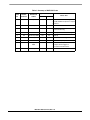
Freescale Semiconductor
Device Errata
MCF5272 Device Errata
This document identifies implementation differences
between the MCF5272 processor and the description
contained in the MCF5272 User’s Manual. Please check
the world wide web at http:/freescale.com for the latest
updates.
This document replaces XCF5272DE/D and applies to
mask sets 1K75N and 3K75N. Designers can
differentiate between the two mask sets according to the
following guidelines:
• The SIMBC device ID register (DIR) has a
32-bit value of 0x2440 301D for 1K75N and
0x4440 301D for 3K75N.
• The JTAG ID register has a 32-bit value of
0x2440 301D for 1K75N and 0x4440 301D for
3K75N.
• The USB specification number register
(SPECR) has a 16-bit value of 0x1101 for
1K75N and 0x1104 for 3K75N.
Table 1 summarizes the MCF5272 errata.
© Freescale Semiconductor, Inc., 2004. All rights reserved.
MCF5272DE
Rev. 1.8, 02/2005
Table 1. Summary of MCF5272 Errata
Errata
ID
Module
Affected
Date Errata
Added
1
USB
2
Applicable Mask Set
Errata Title
1K75N
3K75N
21 May 2001
Yes
No
USB module sends zero length packet
instead of NAK in response to request
from host
All
30 January 2003
Yes
Yes
ESD
3
PLIC
17 October 2001
Yes
No
Observed effects of receive byte
synchronization bug
4
FEC
3 December 2002
Yes
Yes
FEC duplicate transmission bug
5
All
30 January 2003
Yes
Yes
Latch-up
6
SDRAM
27 February 2003
Yes
Yes
SDRAM 256Mbit configuration error
7
GPIO
4 December 2003
Yes
Yes
Weak internal pull up active after reset
8
FEC
14 September
2004
Yes
Yes
Late collision, retry limit, and underrun
interrupts will not trigger on
consecutive transmit frames
9
FEC
15 February 2004
Yes
Yes
FEC MII Invalid Preamble
MCF5272 Device Errata, Rev. 1.8
2
Freescale Semiconductor
USB Module Sends Zero Length Packet Instead of NAK in Response to Request from Host
1
USB Module Sends Zero Length Packet Instead
of NAK in Response to Request from Host
This errata applies to all USB Endpoint Control Registers (EPnCTL).
1.1
Description of Problem
The USB module issues a zero-length data packet instead of a NAK when an endpoint receives an IN
request (device-to-host transfer) and the endpoint has no data to send. Refer to Table 8-2 of USB v1.1
specification (section 8.4.5.1). This problem manifests itself when communicating with PCs running the
Microsoft Windows Communications Device Class USB driver. This driver is normally included with the
Windows Millennium Edition operating system and upgrades for the Windows 98 operating system. The
Windows USB Communications Device Class driver responds with an ACK to the zero-length packet
returned by the MCF5272 and then no longer generates any further tokens.
On the MCF5272, the response to an IN request is controlled by the IN_DONE bit. There is an IN_DONE
bit associated with each of the 8 endpoints. See descriptions for Endpoint Control Registers, EPnCTL.
When the IN_DONE bit is set, the USB module only sends maximum size packets or NAK responses if
the FIFO (first-in, first out) contains less than a maximum packet size. If the bit is cleared, the USB module
sends any amount of data in the FIFO or zero-length packets when the FIFO is empty. By default, this bit
is cleared.
The IN_DONE bit operates as follows:
This bit controls the USB module’s response to IN packets from the host. This bit must be set at the
beginning of a transfer and cleared after all data for the transfer has been written to the FIFO. This bit
allows transfers to be handled correctly.
1 = CPU Busy writing transfer into the IN FIFO. The USB module will only send maximum size packets
or NAK responses if the FIFO contains less than a maximum size packet.
0 = CPU Done writing transfer into the IN FIFO. The USB module will send any amount of data in the
FIFO or zero-length packets when the FIFO is empty.
Mask affected: 1K75N
1.2
1.2.1
Workarounds
Software Workaround 1
A software workaround has been identified that requires the IN_DONE bit to be set by software at all
times. This bit should only be cleared when all of the data for a transfer has been placed into the FIFO. At
this point, the USB module will send a partial or zero-length packet indicating the end of a transfer. The
software should then reset the IN_DONE bit so that no more zero-length packets are sent. The
End-of-Transfer (EOT) status bit should be used (interrupt or polling) to know when to reset the IN_DONE
bit. However, it may not be guaranteed that the application software will be able to reset the IN_DONE bit
MCF5272 Device Errata, Rev. 1.8
Freescale Semiconductor
3
USB Module Sends Zero Length Packet Instead of NAK in Response to Request from Host
before the host sends another IN request. This timing could vary greatly with processor speed, operating
system (device and host), host USB controller, etc.
1.2.2
Software Workaround 2
Provide a product specific USB host driver that substitutes for the standard Microsoft Communications
device class driver. This driver should take into account the MCF5272 USB interface software solution
described above.
MCF5272 Device Errata, Rev. 1.8
4
Freescale Semiconductor
\ESD
2
\
ESD
2.1
1K75N
ESD HBM testing passes 1 kV, except for the USB_D+ and USB_D– pins, which pass 700 V. ESD MM
testing passes 100 V, except for the USB_D+ and USB_D– pins, which pass 75 V.
2.2
3K75N
ESD HBM testing passes 1kV for all pins. ESD MM testing passes 100 V for all pins.
MCF5272 Device Errata, Rev. 1.8
Freescale Semiconductor
5
PLIC Byte Synchronization Bug
3
PLIC Byte Synchronization Bug
3.1
Description of Problem
The receiving order of the B and D channel data can become scrambled due to the 8-KHz frame counters
becoming unsynchronized. Upon a given RESET of the device, the data is always scrambled in the same
manner; however, the error pattern may differ after each successive RESET.
Mask affected: 1K75N
3.2
Description of Fix
A comprehensive fix has been implemented in silicon for masks 3K75N and above, which corrects the
observed effects of the bug in Table 2. The fix implements a single synchronization counter for all PLIC
channels. Freescale has confirmed the fix with simulations using unique data for each byte of each channel.
Table 2. Observed Effects of Receive Byte Synchronization Bug
Configuration
PLCR1 [b9] = 0 (FSM)
Port 0 = IDL-GCI slave, Port 1 = IDL-GCI slave
PLCR1 [b9] = 1 (FSM)
Port 0 OK, Port 1 shows bug Port 0 shows bug, Port 1 shows bug
Port 0 = IDL-GCI slave, Port 1 = IDL-GCI master Port 0 OK, Port 1 shows bug Port 0 OK, Port 1 shows bug
Port 0 not used, Port 1 = IDL-GCI slave
Does not apply
Port 1 shows bug
Port 0 = IDL-GCI slave, Port 1 not used
No bug
Does not apply
3.3
3.3.1
Workarounds
Software Workaround for Port 1 Master
When initializing the PLIC ports, port 1 should be configured as a master before writing to the PORT A
and PORT D pin configuration registers to set the FSC0 and DCL0 pins to be PLIC pins (reset state is PA8
and hiZ). This will ensure that the super-frame sync generator and port 1 always see the same FSC, and
therefore will stay in sync.
3.3.2
Hardware Workaround for Port 1 Slave
The hardware workaround for using Port 1 in slave mode is to ensure that the FSC is not free-running prior
to enabling the port and is restricted to one of two cases:
1. If Port 0 is used, make sure the same FSC is connected to FSC0 and FSC1, as well as not having a
free-running FSC prior to enabling the port.
2. If Port 0 is unused and receives no frame syncs, verify there is no free-running FSC prior to
enabling the port. This will ensure that the data remains in sync.
MCF5272 Device Errata, Rev. 1.8
6
Freescale Semiconductor
PLIC Byte Synchronization Bug
3.3.3
Software Workaround for Port 2 and Port 3
In this case, in order to use Ports 2 and 3, the user must multiplex Port 3 with Port 2, as opposed to using
Port 3 with dedicated inputs and outputs. The Port 1 sync delay register should then be used to create a
delayed FSC1, which should be equal to the number of DCL clocks in a frame minus one, followed by a
delayed FSC2 and FSC3 to place Port 2 and Port 3 in the appropriate timeslots. Below is an example of
the settings for the port configuration registers and sync delay registers using a DCL = 384 KHz:
P1CR = 0x8A00
(FSM = 1, B1 and B2 disabled)
P2CR = 0x8003
P3CR = 0x8003
P1SDR = 0x002F
(47 decimal)
P2SDR = 0x0008
(port2 start 8 clocks after FSC1)
P3SDR = 0x0018
(port3 start 24 clocks after FSC1)
NOTE
Always use the same universal clock for FSC0 and FSC1.
MCF5272 Device Errata, Rev. 1.8
Freescale Semiconductor
7
FEC Duplicate Transmission Bug
4
FEC Duplicate Transmission Bug
4.1
Description
In some cases, the FEC will transmit single frames more than once. The FEC fetches transmit buffer
descriptors (TxBDs) and the corresponding Tx data continuously until the Tx FIFO is full. It does not
determine whether the TxBD to be fetched is already being processed internally (as a result of a wrap). As
the FEC nears the end of the transmission of one frame, it begins to DMA the data for the next frame. In
order to remain one BD ahead of the DMA, it also fetches the TxBD for the next frame. It is possible that
the FEC will fetch from memory a BD that has already been processed but not yet written back (that is, it
is read a second time with the R bit still set). In this case, the data is fetched and transmitted again.
Masks affected: 1K75N & 3K75N
4.2
Workaround
Using at least three TxBDs fixes this problem for large frames, but not for small frames. To ensure correct
operation for either large or small frames, one of the following must be true:
• The FEC software driver ensures that there is always at least one TxBD with the Ready bit cleared
• Every frame uses more than one TxBD and every TxBD but the “last” is written back
immediately after the data is fetched
• The FEC software driver ensures a minimum frame size, n. The minimum number of TxBDs is
then Tx FIFO Size ÷ ( n + 4 ) rounded up to the nearest integer (though the result cannot be less than 3).
The default Tx FIFO size is 192 Bytes; this size is programmable.
MCF5272 Device Errata, Rev. 1.8
8
Freescale Semiconductor
Latch-Up
5
Latch-Up
5.1
1K75N & 3K75N
Both mask sets pass 75mA latch-up.
MCF5272 Device Errata, Rev. 1.8
Freescale Semiconductor
9
SDRAM 256 Mbit Configuration Errors
6
SDRAM 256 Mbit Configuration Errors
6.1
Description
The SDRAM configuration using two 16-bit-wide, 256-Mbit SDRAM chips does not work. There is an
error in the page mode logic that prevents the SDRAM controller from correctly tracking which pages are
currently open when using this configuration. All other SDRAM configurations documented in the 5272
user’s manual work correctly and are unaffected by this errata.
Masks affected: 1K75N & 3K75N
6.2
Workaround
No workaround. Use one of the other SDRAM configurations.
MCF5272 Device Errata, Rev. 1.8
10
Freescale Semiconductor
Weak Internal Pull Up Active after Reset
7
Weak Internal Pull Up Active after Reset
7.1
Description
After reset, the GPIO pins are all configured as GPIO inputs. However, until they are configured as GPIO
inputs by software, there is a weak internal pull up resistor active on these pins. The pull up resistance is
approximately 5 kΩ. If the pin is programmed as a GPIO input, the internal pull up is disabled.
Masks affected: 1K75N & 3K75N
7.2
Workaround
No workaround. Pull down resistor values should take into account the internal pull up value.
7.3
Workaround
No workaround. Pull down resistor values should take into account the internal pull up value.
MCF5272 Device Errata, Rev. 1.8
Freescale Semiconductor
11
Late Collision, Retry Limit, and Underrun Interrupts will not Trigger on Consecutive Transmit Frames
8
Late Collision, Retry Limit, and Underrun
Interrupts will not Trigger on Consecutive
Transmit Frames
8.1
Description
The late collision (LC), retry limit (RL), and underrun (UN) interrupts will not trigger on consecutive
transmit frames. For example, if back-to-back frames cause a transmit underrun, only the first frame will
generate an underrun interrupt. No other underrun interrupts will be generated until a frame is transmitted
that does not underrun or the FEC is reset.
8.2
Workaround
Since late collision, retry limit, and underrun errors are not directly correlated to a specific transmit frame,
in most cases a workaround for this problem is not needed. If a workaround is required, then there are two
independent workarounds:
• Ensure that a correct frame is transmitted after a late collision, retry limit, or underrun errors are
detected.
• Perform a soft reset of the FEC by setting ECR[RESET] when a late collision, retry limit, or
underrun errors are detected.
DATECODES AFFECTED: All
MCF5272 Device Errata, Rev. 1.8
12
Freescale Semiconductor
FEC MII Invalid Preamble
9
FEC MII Invalid Preamble
9.1
Description of Problem
The FEC MII interface will intermittently send an incorrect preamble. The error always occurs on the first
nibble of the preamble. Instead of the specified value of ETXD[3:0] = b'0101, ETXD3 will be a logic '1'
resulting in ETXD[3:0] = b'1101. Some Ethernet physical layer interface devices will discard this packet.
9.2
9.2.1
Workarounds
Software Workarounds
Rely on network protocol stacks and upper-level network applications to resend the discarded packet.
9.2.2
Hardware Workarounds
1. Some Ethernet physical interface devices are immune to this preamble fault.
2. It is possible to detect the fault in an external programmable device. The faulty preamble nibble
will always occur in the first transaction following the assertion of ETXEN. Therefore, ETXD3
could be routed through an external device which could detect and correct the faulty preamble
before it reaches the PHY.
MCF5272 Device Errata, Rev. 1.8
Freescale Semiconductor
13
FEC MII Invalid Preamble
THIS PAGE INTENTIONALLY LEFT BLANK
MCF5272 Device Errata, Rev. 1.8
14
Freescale Semiconductor
THIS PAGE INTENTIONALLY LEFT BLANK
MCF5272 Device Errata, Rev. 1.8
Freescale Semiconductor
15
How to Reach Us:
Home Page:
www.freescale.com
E-mail:
[email protected]
USA/Europe or Locations Not Listed:
Freescale Semiconductor
Technical Information Center, CH370
1300 N. Alma School Road
Chandler, Arizona 85224
+1-800-521-6274 or +1-480-768-2130
[email protected]
Europe, Middle East, and Africa:
Freescale Halbleiter Deutschland GmbH
Technical Information Center
Schatzbogen 7
81829 Muenchen, Germany
+44 1296 380 456 (English)
+46 8 52200080 (English)
+49 89 92103 559 (German)
+33 1 69 35 48 48 (French)
[email protected]
Japan:
Freescale Semiconductor Japan Ltd.
Technical Information Center
3-20-1, Minami-Azabu, Minato-ku
Tokyo 106-0047, Japan
0120 191014 or +81 3 3440 3569
[email protected]
Asia/Pacific:
Freescale Semiconductor Hong Kong Ltd.
Technical Information Center
2 Dai King Street
Tai Po Industrial Estate
Tai Po, N.T., Hong Kong
+800 2666 8080
[email protected]
For Literature Requests Only:
Freescale Semiconductor Literature Distribution Center
P.O. Box 5405
Denver, Colorado 80217
1-800-441-2447 or 303-675-2140
Fax: 303-675-2150
[email protected]
Information in this document is provided solely to enable system and
software implementers to use Freescale Semiconductor products. There are
no express or implied copyright licenses granted hereunder to design or
fabricate any integrated circuits or integrated circuits based on the
information in this document.
Freescale Semiconductor reserves the right to make changes without further
notice to any products herein. Freescale Semiconductor makes no warranty,
representation or guarantee regarding the suitability of its products for any
particular purpose, nor does Freescale Semiconductor assume any liability
arising out of the application or use of any product or circuit, and specifically
disclaims any and all liability, including without limitation consequential or
incidental damages. “Typical” parameters that may be provided in Freescale
Semiconductor data sheets and/or specifications can and do vary in different
applications and actual performance may vary over time. All operating
parameters, including “Typicals”, must be validated for each customer
application by customer’s technical experts. Freescale Semiconductor does
not convey any license under its patent rights nor the rights of others.
Freescale Semiconductor products are not designed, intended, or authorized
for use as components in systems intended for surgical implant into the body,
or other applications intended to support or sustain life, or for any other
application in which the failure of the Freescale Semiconductor product could
create a situation where personal injury or death may occur. Should Buyer
purchase or use Freescale Semiconductor products for any such unintended
or unauthorized application, Buyer shall indemnify and hold Freescale
Semiconductor and its officers, employees, subsidiaries, affiliates, and
distributors harmless against all claims, costs, damages, and expenses, and
reasonable attorney fees arising out of, directly or indirectly, any claim of
personal injury or death associated with such unintended or unauthorized
use, even if such claim alleges that Freescale Semiconductor was negligent
regarding the design or manufacture of the part.
Freescale™ and the Freescale logo are trademarks of Freescale
Semiconductor, Inc. All other product or service names are the property
of their respective owners.© Freescale Semiconductor, Inc. 2004. All rights
reserved.
MCF5272DE
Rev. 1.8
02/2005