1
RVCF Quick User Guide
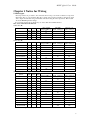
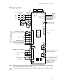
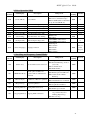
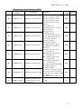
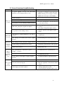
1.4 Description of inverter terminals
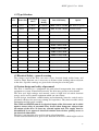
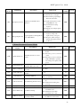
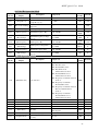
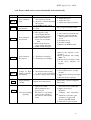
Descriptions of main circuit terminals
Description
Symbol
R / L1 ( L )
S / L2
T / L3 ( N )
P1
BR
P1/ P
B1/P
B2
Ө
Main power input
Braking resistor or connecting terminal: Used in cases where the inverter
frequently disconnects due to large load inertia or short deceleration time
(refer to specifications of braking resistor)
DC reactor connecting terminals
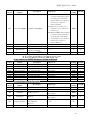
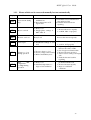
B 1 /P - Ө : D C p o wer s up p l y i np u t
B 1 /P -B 2 : E xt er na l b r a k i n g r es i sto r
Fo r 2 3 0 V: 1 5 ~2 0 HP a nd 4 8 0 V: 2 0 HP
-
⊕
U / T1
V / T2
W / T3
Single-phase: L/N
Three-phase: L1/L2/L3
-
⊕ - Ө : D C p o we r s up p l y inp u t o r
E x ter na l b r a ki n g u n it. Check Chapter 6.3
Fo r 2 3 0 V: 2 5 ~4 0 HP a nd 4 8 0 V: 2 5 ~7 5 HP
Inverter outputs
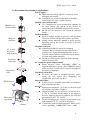
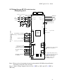
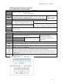
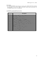
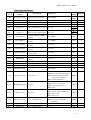
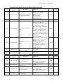
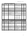
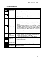
Descriptions of RVCF control circuit terminals
Symbol
Description
R2A
Multifunctional terminal – Normal open
R2B
Common contact
R1C
Normal close contact
Multifunctional output terminals
R1B
Normal open contact
R1A
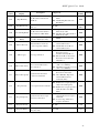
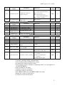
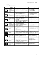
Frequency knob (VR) power source terminal (pin 3)
10V
AIN
24V
COM
24G
AGND
FM+
For
230V:0.5~10HP,
480V:1~15HP
Contact rated capacity:
(250VAC/1A or 30VDC/1A)
Contact using description:(refer to
8-02, 8-03)
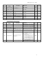
Analog frequency signal input terminal or multifunction input terminals S7 (H level:>8V, L level:<2V,
PNP only) (refer to5-06 description)
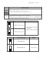
Common contact for S1~S5 (S6, S7) in PNP (Source) input. Shift to PNP position (refer to wiring
diagram) of SW1 when used PNP input
1. Common contact and analog input /output signal for S1~S5 in NPN (Sink) input.
Shift to NPN position (refer to wiring diagram I) of SW1 when used NPN input.
2. AGND for AIN,AI2 and FM+ (analog input /output signal) & 24G for S1~S6 (digital input /output
signal in NPN (Sink) input). Shift to NPN position (refer to wiring diagram II) of SW1 when used
NPN input.
The positive analog output for multifunction (refer to 8-00 description), the signal for output terminal is
0-10VDC (below 2mA).
14