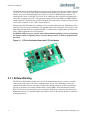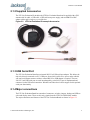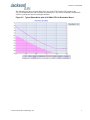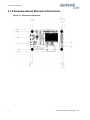
1
LTE-Lite(tm) User
Manual
Document:
80200522
Version:
1.3
Date:
6 November, 2014
LTE-Lite User Manual
Copyright © 2013, 2014 Jackson Labs Technologies, Inc.
LTE-Lite User Manual
1 Introduction
. . . . . . . .
1.1 Overview . . . . . . . . . .
1.2 General Safety Precautions . . .
1.2.1 Grounding . . . . . . .
1.2.2 Antenna Lightning Protection
1.2.3 Power Connections. . . .
1.2.4 Environmental Conditions .
.
.
.
.
.
.
.
.
.
.
.
.
.
.
.
.
.
.
.
.
.
.
.
.
.
.
.
.
.
.
.
.
.
.
.
.
.
.
.
.
.
.
.
.
.
.
.
.
.
.
.
.
.
.
.
.
.
.
.
.
.
.
.
.
.
.
.
.
.
.
.
.
.
.
.
.
.
.
.
.
.
.
.
.
.
.
.
.
.
.
.
.
.
.
.
.
.
.
.
.
.
.
.
.
.
.
.
.
.
.
.
.
.
.
.
.
.
.
.
.
.
.
.
.
.
.
.
.
.
.
.
.
.
.
.
.
.
.
.
.
.
.
.
.
.
.
.
. . . . . . . . . . . . . . . . . . . . .
Powering Up the Evaluation Board . . . . . . . . . . . . . . . . .
2.1.1 Airflow Warning . . . . . . . . . . . . . . . . . . . . . .
2.1.2 Supplied Accessories . . . . . . . . . . . . . . . . . . . .
2.1.3 USB Serial Port . . . . . . . . . . . . . . . . . . . . . .
2.1.4 Major connections . . . . . . . . . . . . . . . . . . . . .
2.1.5 Typical Phase Noise and ADEV Plots . . . . . . . . . . . . .
2.1.6 Evaluation Board Mechanical Dimensions . . . . . . . . . . . .
2.1.7 LTE-Lite SMT Module Mechanical Dimensions . . . . . . . . . .
2.1.8 LTE-Lite Evaluation Board Schematics . . . . . . . . . . . . .
Connector, Buttons and Switches on the Evaluation Board . . . . . . . .
LTE-Lite SMT Module usage . . . . . . . . . . . . . . . . . . .
2.3.1 LTE-Lite SMT Module Minimum Required Setup . . . . . . . . .
2.3.2 Using the LTE-Lite SMT Module with external TCXOs . . . . . . .
2.3.3 Using the LTE-Lite SMT Module Synthesized Frequency Output . . .
2.3.4 Adding a USB output to the LTE-Lite SMT Module for NTP applications
2.3.5 SMT Module Power Connection . . . . . . . . . . . . . . . .
2.3.6 SMT Module Antenna Connection . . . . . . . . . . . . . . .
2.3.7 1PPS Module outputs . . . . . . . . . . . . . . . . . . . .
2.3.8 Synthesized RF Output Frequency. . . . . . . . . . . . . . .
2.3.9 System Reset . . . . . . . . . . . . . . . . . . . . . . .
2.3.10Module Serial IO pins . . . . . . . . . . . . . . . . . . . .
2.3.11Module IO Pinout . . . . . . . . . . . . . . . . . . . . .
Connecting a GPS Antenna . . . . . . . . . . . . . . . . . . . .
USB serial connection . . . . . . . . . . . . . . . . . . . . . .
2.5.1 Proprietary $PSTI NMEA GPS Status Sentence . . . . . . . . .
2.5.2 JLT Proprietary STATUS Output Sentence . . . . . . . . . . .
2.5.2.1 Lock Status Definition . . . . . . . . . . . . . . . .
2.5.2.2 Health Status Definition . . . . . . . . . . . . . . . .
.
.
.
.
.
.
.
.
.
.
.
.
.
.
.
.
.
.
.
.
.
.
.
.
.
.
.
.
.
.
.
.
.
.
.
.
.
.
.
.
.
.
.
.
.
.
.
.
.
.
.
.
.
.
.
.
.
.
.
.
.
.
.
.
.
.
.
.
.
.
.
.
.
.
.
.
.
.
.
.
.
.
.
.
.
.
.
. 3
. 3
. 4
. 5
. 5
. 5
. 6
. 8
. 9
. 9
. 11
. 13
. 13
. 14
. 16
. 17
. 18
. 18
. 18
. 18
. 19
. 20
. 20
. 24
. 25
. 25
. 25
. 26
. 26
.
.
.
.
.
.
.
.
.
.
.
.
.
.
.
. 27
. 27
. 27
. 27
. 28
2 Usage Instructions
2.1
2.2
2.3
2.4
2.5
3 Certification and Warranty .
3.1 Certification . . . . . . .
3.1.1 Warranty . . . . . .
3.1.2 Limitation of Warranty .
3.1.3 Exclusive Remedies .
© 2014 Jackson Labs Technologies, Inc.
.
.
.
.
.
.
.
.
.
.
.
.
.
.
.
.
.
.
.
.
.
.
.
.
.
.
.
.
.
.
.
.
.
.
.
.
.
.
.
.
.
.
.
.
.
.
.
.
.
.
.
.
.
.
.
.
.
.
.
.
.
.
.
.
.
.
.
.
.
.
.
.
.
.
.
.
.
.
.
.
.
.
.
.
.
.
.
.
.
.
.
.
1
1
2
2
2
2
2
i
LTE-Lite User Manual
ii
© 2014 Jackson Labs Technologies, Inc.
LTE-Lite User Manual
Introduction
1.1 Overview
The LTE-Lite GPSDO is a very low-cost, small SMT Timing and Frequency reference module for
high-volume Small Cell applications. It is intended to provide precise timing and a very low Phase
Noise and jitter frequency reference to RF Transceivers and Base Band processors as typically used
in Small Cell applications. The LTE-Lite is a true GPSDO rather than a Numerically Controlled
Oscillator, using true precision analog disciplining of the high-end Crystal rather than digital
phase-adjustments of a free running low-cost crystal, resulting in many orders of magnitude less jitter
and Phase Noise. The LTE-Lite GPSDO is available as an SMT module, or mounted onto the
LTE-Lite Evaluation Board with easy access to relevant signals via a host of connectors and
switches.
The LTE-Lite GPSDO and LTE-Lite Evaluation Board include a high-performance GPS/QZSS
receiver that can acquire and track up to 65 GPS signals down to a state of the art –165dBm, a 32bit
processor, a low-noise 3V CMOS 10MHz, 19.2MHz, or 20MHz output, two 3.3V CMOS 1PPS
outputs, TTL or USB status and Position-Velocity-and-Time (PVT) interface, precision voltage
references, power filters, and DACs. It generates a low-noise 10/19.2/20MHz signal with typically
better than 1E-09 precision and accuracy (1ppb), better than typ. 135fs jitter (100Hz to 2MHz) and a
1PPS signal with typically better than +/-25ns stability when locked to GPS.
The LTE-Lite GPSDO provides status information on TTL output lines that can directly drive LEDs,
and has two serial output ports for NMEA PVT and Oscillator status output. All configuration of the
LTE-Lite GPSDO is done via pull-down TTL straps with built-in pull-up resistors, so no software
configuration driver is needed on the users’ system. The evaluation kit may be operated and powered
from the built-in USB port, or an optional 5V power supply and both power-sources may be
connected simultaneously. The evaluation kit is supplied with a USB cable and matching wall-wart
power supply, two MMCX to BNC adaptor cables, a GPS antenna, and a quick-start guide. The unit
provides an industry-standard NMEA GPS serial output that is enabled by default and provides
Position/Velocity/Timing (PVT) information, and also provides a UTC-synchronized 1PPS signal on
the USB serial port DCD# pin for NTP applications. The LTE-Lite GPSDO also provides a
NMEA-compatible proprietary status message on a secondary serial port that sends oscillator lock
status as well as health status information to a users’ system.
© 2014 Jackson Labs Technologies, Inc.
1
LTE-Lite User Manual
1.2 General Safety Precautions
The following general safety precautions must be observed during all phases of operation of this
instrument. Failure to comply with these precautions or with specific warnings elsewhere in this
manual violates safety standards of design manufacture, and intended use of the instrument. Jackson
Labs Technologies, Inc. assumes no liability for the customer’s failure to comply with these
requirements.
1.2.1 Grounding
To avoid damaging the sensitive electronic components in the LTE-Lite GSPDO kit or board always
make sure to discharge any built-up electrostatic charge to a good ground source, such as power
supply ground. This should be done before handling the circuit board or anything connected to it, i.e.
the GPS antenna.
1.2.2 Antenna Lightning Protection
Always use a UL-certified, properly installed Antenna Lightning suppressor on the antenna cable
when mounting the GPS antenna. Without proper Lightning Protection damage to equipment, injury,
or death may result.
1.2.3 Power Connections
Make sure to connect the DC power to the device following the polarity indicated in Section 2.1 . Do
not reverse the power pins as this will cause serious damage to the circuit board.
1.2.4 Environmental Conditions
This instrument is intended for indoor use. It is designed to operate at a maximum relative
non-condensing humidity of 95% and at altitudes of up to 4000 meters. Refer to the specifications
tables for the ac mains voltage requirements and ambient operating temperature range.
2
© 2014 Jackson Labs Technologies, Inc.
LTE-Lite User Manual
Usage Instructions
2.1 Powering Up the Evaluation Board
The LTE-Lite Evaluation Board is essentially a plug-and-play product that only requires a power
source and a GPS antenna to be connected to start generating highly-accurate output frequency and
1PPS signals that are phase and frequency aligned to UTC (USNO) and thus allow NIST-tracability.
To use the Evaluation Board, simply plug in the power supply using the supplied USB cable, plug in
the antenna, and wait about 15 minutes typically for the GREEN “LOCK-OK” LED to light up to
indicate that the unit is locked to UTC with better than +/-250ns phase accuracy, and a frequency
accuracy of better than 1ppb has been achieved. The internal software will auto-configure and
auto-calibrate the unit without any user-interaction and the longer the unit runs the more accurate it
will become.
For units with a Timing GPS receiver, the unit will start an Auto Survey process to establish the
stationary antenna position as soon as power is applied, and this is indicated by the SURVEY LED on
the Evaluation Board. The Auto Survey process will take at least 2000 seconds to finish, at which
time the antenna position is stored in internal memory, and operation with 1 satellite is possible (4
sats are required for Mobile mode/non-Position-Hold operation).
The Evaluation Board is powered directly from the USB cable, and/or from an optional external 5V
DC source on the +5V header. The USB cable and the external 5V DC source may be connected at
the same time as they are diode-protected from one another. The current is typically less than 0.07A
at 5V. Connect a clean +5V power supply to the +5V header block if the USB cable is not going to be
used, or is plugged-in intermittently. See Figure 2.3 for the proper polarity of the optional external
5V DC power connection. Reversing the polarity on the power connector will not damage the unit as
it is diode reverse-polarity protected.
When communicating to the unit through the USB cable, Windows Vista, Windows 7/8 and Linux
will auto-recognize the unit as a USB serial COM adaptor, and automatically assign a serial port to
the unit. Windows will automatically load the USB COM driver for the board, and may need to have
access to the Internet to download the latest driver from the Microsoft update website. The user can
verify the COM port that windows assigned to the unit under the Computer Management window
(right click on computer and press the “MANAGE” button under Windows 7, or go to Control
Panel/Computer Management). The unit should show up as a standard serial port adaptor under the
“Ports (COM& LPT)” Icon. Please note the COM port number, as it is required for the initialization
of application software.
© 2014 Jackson Labs Technologies, Inc.
3
LTE-Lite User Manual
The unit will start to search for satellites as soon as power is applied, and will start to lock the internal
TCXO to UTC as soon as a GPS antenna is attached and more than 4 sats become visible. After 30
minutes or less the unit should stabilize the frequency, and all ALARM indicators should be off
resulting in the Green “LOCK OK” LED to be lit up. At this time the Green LED will indicate the
unit is fully synchronized to UTC, and generating a stable and accurate 20MHz/19.2MHz/10MHz
output signal. The Green LED may go off momentarily from time to time as airflow touches the unit
or sats come in and out of view - this is normal behavior.
You may place the GPS antenna in a window, but it is recommended to place the GPS antenna with a
full view of the sky for best performance. The antenna cable can be extended to 100m or more with
high quality antenna cable (use quad shielded RG-6 75 Ohms cable, or high-quality 50 Ohms coax
cable) without significant loss of signal quality.
WARNING: Make sure to use a proper and certified Antenna Lightning Arrestor when placing
the antenna outside as lightning strikes can cause damage, injury, or death to equipment and
personnel.
Figure 2.1
LTE-Lite Evaluation Board with LTE-Lite Module
2.1.1 Airflow Warning
The LTE-Lite SMT module and thus the LTE-Lite Evaluation Board are very sensitive to airflow.
This includes airflow from convection, walking past the unit, or Air Conditioning systems. For
optimal performance the user must insure that the unit is shielded from any airflow by placing the
unit into an enclosure (for example Hammond PN: 1455C801BK). Please note that the external
DIP-14 TCXO and its socket must be removed from the PCB for it to fit into the aforementioned
Hammond enclosure. For optimal stability performance of the TCXO the unit should be sealed into
an airtight enclosure.
4
© 2014 Jackson Labs Technologies, Inc.
LTE-Lite User Manual
2.1.2 Supplied Accessories
The LTE-Lite Evaluation Kit includes the LTE-Lite Evaluation Board and is supplied with a GPS
antenna with 5m cable, a USB cable, a USB wall-wart power supply, and two MMCX to BNC
adaptor cables and is ready-to-go out of the box.
Figure 2.2
LTE-Lite Evaluation Kit example Accessories
2.1.3 USB Serial Port
The LTE-Lite Evaluation Board has an internal RS-232 to USB serial port adaptor. This allows the
unit to be directly connected to a PC’s USB port, from which it will receive power and to which it
will send serial output sentences with no external RS-232 to USB adaptor is required. The term
“RS-232” and USB serial port are used interchangeably, as the RS-232 port is implemented and
connected via the USB serial connection. Windows and Linux have built-in support for this optional
serial port functionality.
2.1.4 Major connections
The LTE-Lite Evaluation Board has a number of connectors, switches, jumpers, headers and LEDs to
select and display status. These are driven by signals from the LTE-Lite GPSDO SMT module.
The major connections and features of the LTE-Lite Evaluation Board are shown in Figure 2.3.
© 2014 Jackson Labs Technologies, Inc.
5
LTE-Lite User Manual
Figure 2.3
Major connections of the LTE-Lite Evaluation Board
2.1.5 Typical Phase Noise and ADEV Plots
The following plot shows a typical ADEV plot for the LTE-Lite Evaluation Board. The unit had been
operating for 5+ days, has not been moved or vibrated in any way, and was completely shielded from
airflow by placing the unit into an airtight enclosure.
Figure 2.4
6
Typical ADEV plot of 20MHz LTE-Lite Evaluation Board
© 2014 Jackson Labs Technologies, Inc.
LTE-Lite User Manual
The following plot shows a typical Phase Noise plot of the TCXO buffered RF output for the
LTE-Lite Evaluation Board. The unit had been operating for 1 day, and was completely shielded from
airflow by placing the unit into an airtight enclosure.
Figure 2.5
Typical Phase Noise plot of 19.2MHz LTE-Lite Evaluation Board
© 2014 Jackson Labs Technologies, Inc.
7
LTE-Lite User Manual
2.1.6 Evaluation Board Mechanical Dimensions
Figure 2.6
8
Mechanical dimensions
© 2014 Jackson Labs Technologies, Inc.
LTE-Lite User Manual
2.1.7 LTE-Lite SMT Module Mechanical Dimensions
Figure 2.7
Mechanical dimensions of the LTE-Lite SMT Module
2.1.8 LTE-Lite Evaluation Board Schematics
The following schematics may be used as an example of how to connect the LTE-Lite SMT Module,
and to maximize the features of the LTE-Lite SMT Module. Please note that IC U4 is the actual
LTE-Lite SMT module.
© 2014 Jackson Labs Technologies, Inc.
9
LTE-Lite User Manual
Figure 2.8
10
Schematics of LTE-Lite Evaluation Board
© 2014 Jackson Labs Technologies, Inc.
LTE-Lite User Manual
2.2 Connector, Buttons and Switches on the Evaluation Board
Table 2.1 shows the LTE-Lite Evaluation Board connectors, buttons, switches, and LEDs.
Table 2.1 LTE-Lite Evaluation Board connectors, buttons, switches, and LEDs
Ref
Name
Function
Specification
Pinning/Usage
JP2
+5V
Optional External
+5V Supply. Use
when USB power
supply is not
available
5V DC +/-20%, <0.08A, <10mVac
Pin close to USB connector: +5V
Pin close to Mounting Hole: GND
J3
Position Hold
Mode or Mobile
Mode selector
Selects if the unit is
used in stationary
mode or mobile
mode
Open (default): Auto Survey mode
with Position Hold function is
enabled
Jumper Inserted: Auto Survey mode
is disabled, and Mobile (3D) mode is
selected
WARNING: DO NOT CHANGE THE
SETTING OF THIS JUMPER WITH
POWER APPLIED TO THE UNIT,
THIS MAY CORRUPT THE FLASH
OF THE GPS RECEIVER
PERMANENTLY.
Insert a jumper between Pin 1 to Pin
2 to disable Auto Survey mode. Only
change this jumper with power to the
unit being turned off.
WARNING: DO NOT CHANGE THE
SETTING OF THIS JUMPER WITH
POWER APPLIED TO THE UNIT,
THIS MAY CORRUPT THE FLASH
OF THE GPS RECEIVER
PERMANENTLY.
J2
20MHz, 10MHz,
or 19.2MHz
CMOS Out
Buffered RF output
from internal TCXO
+3.0V CMOS 20MHz, 10MHz, or
19.2MHz Output, can drive up to
+/-24mA. Frequency depends on
TCXO selection
Center-RF Output, Shield-GND
J1
1PPS CMOS Out
1PPS Signal
Aligned to UTC
+3.3V CMOS 1PPS Output, can
drive up to +/-10mA
Center-1PPS Output, Shield-GND
U3
USB Port
Supplies Power and
NMEA output strings
Standard USB 2.0 Full Speed
Mini USB
J5
Synthesized RF
output
Un-buffered output
of internal PLL
Synthesizer
3.3V CMOS, can supply up to
+/-10mA, frequency selected via
three jumpers
Center- RF Output, Shield- GND
J4
Antenna In
GPS Antenna
Input
GPS 1575MHz antenna input,
supplies DC +3.3V to antenna
with up to 60mA current
Center- RF Output, Shield- GND
SW1
NMEA/Status
Selector Switch
Selects if either
GPS NMEA data
or an Oscillator
Status sentence is
sent to USB port
For GPS NMEA output: 38.4K
Baud 8N1, supported sentences:
GGA, GLL, GSA, GSV, RMC,
VTG, ZDA
For Status output: 38.4K Baud
8N1, oscillator and system
health status string. Proprietary
NMEA sentence
Left: GPS NMEA
Right: Oscillator Status
© 2014 Jackson Labs Technologies, Inc.
11
LTE-Lite User Manual
SW2
External TCXO
Selector
Disables internal
TCXO and selects
optional external
DIP-14 TCXO
Down setting: external DIP-14
TCXO supplied with +3.3V, and
0V to 3.0V EFC range. TTL or
CMOS output,
10/15.36/19.2/20MHz TCXO
Up: Internal TCXO
Down: External TCXO
SW3
ISP Mode
Selector
Enables In
System
Programming
(ISP) mode
Factory Use Only
Factory Use Only. Set to Right
setting (NORM) for board to
operate properly
S1
Init Auto
Survey
Initiates a
Position Auto
Survey
Press button for 1+ seconds to
manually initiate an Auto
Survey process
Press button for 1+ seconds until
SURVEY LED lights up
S2
RESET
System Reset
Press button momentarily
Initiates a System Reset
LED D5
SURVEY LED
Lights up during
Auto Survey
process
Lights up for 2000 or more
seconds after power-on to
indicate Auto Survey is in
process
Lights up during Auto Survey
LED D6
LOCK-OK
Indicates No
Events are
pending, and
oscillator is
locked
Lights up when oscillator is
locked to UTC via GPS
receiver, and no events are
pending. Events are
individually shown in the status
serial string sentence
Lights up when unit is healthy
and locked to GPS. Extinguishes
when a hardware or software
event is pending, no GPS signal
is received, or the unit is not yet
locked to GPS/UTC
LED D7
WARMUP
Indicates unit is
still in warmup
mode
Lights up for one or more
minutes after power-on
Indicates unit is warming up
LED D8
ALARM
Indicates a
hardware fault, or
software alarm
Lights up when a hardware fault
or software alarm has been
detected
Lights up during Alarm
conditions
GPS
LED
GPS Status
LED
Power and GPS
Fix indicator
Lights up when power is
applied, and blinks when GPS
fixes are being received
Blinks when GPS fixes are
properly being received, and unit
is powered-on. Resides on
LTE-Lite SMT module near
antenna connector
12
© 2014 Jackson Labs Technologies, Inc.
LTE-Lite User Manual
JP1
Debug
Connector
Debug status,
Synthesizer
Frequency
selector, 1Hz/5Hz
NMEA selector,
Raw 1PPS output,
RESET# output
signal
Pins 9, 10, and 11: Insert
jumpers
Pins 12 and 13: CMOS 3.3V
output of GPS 1PPS and GPS
TXD
Pin 14: Insert jumper for 5Hz
NMEA output
Pin 15: Indicates when
synthesizer is phase-locked (can
be used as a RESET# signal to
other circuits)
Pin 16: +3.3V, 50mA max
Insert jumpers between Pins 9
and 8, 10 and 7, 11 and 6 to
select synthesized output
frequency.
Insert jumper between pin 14
and 3.
Pin 15: standard 3.3V CMOS
level RESET# output signal with
up to 1s reset active low
2.3 LTE-Lite SMT Module usage
The LTE-Lite SMT Module by itself is designed to be soldered into a customer PCB using standard
SMT pick-and-place procedures. The SMT module is designed as a 0.032 inches thin single-sided
PCB with 32 castellated solder pads on the bottom and on the sides of the module. It is recommended
that the users’ PCB has a filled ground plane under the SMT module, and does not contain any traces
under the SMT module to avoid cross-talk into signals inside the module. It is also recommended that
the users’ PCB has a solid silkscreen layer under the SMT module to generate insulation between the
SMT module and the users’ PCB. Soldering can be done manually, or using standard reflow oven
soldering procedures. The module can be soldered onto the customers’ PCB using lead or RoHs
procedures.
The LTE-Lite SMT module is moisture sensitive, and it must be pre-baked before
reflow-soldering to avoid damage to the internal IC’s from moisture absorbtion. Pre-bakeing
should be done at +110 Degrees C maximum for 24 hours prior to soldering the module to a
customers’ PCB. Pre-bakeing is not required for manually hand-soldering the unit onto a
customers’ PCB using a solder-iron (not a heat-gun).
2.3.1 LTE-Lite SMT Module Minimum Required Setup
The following schematics show the minimum required connections to operate the LTE-Lite SMT
Module. Only a +3.3V power supply is needed, an antenna connection to the internal U.Fl coax
connector, and a connection to the TCXO output and 1PPS output are needed to use the module.
© 2014 Jackson Labs Technologies, Inc.
13
LTE-Lite User Manual
Figure 2.9
Minimum required setup for the LTE-Lite SMT Module
2.3.2 Using the LTE-Lite SMT Module with external TCXOs
The following schematics shows how to connect an external 3.0V TCXO to the LTE-Lite SMT
Module using the internal low-noise 3.0V regulator output to power the external TCXO. The internal
TCXO and TCXO buffer are disabled by pulling the DISABLE-TCXO pin 8 of the module high,
14
© 2014 Jackson Labs Technologies, Inc.
LTE-Lite User Manual
which then allows feeding an external 3.3V CMOS or TTL RF signal into the RF pin 6 of the
module. The former RF output pin 6 of the module becomes an RF input pin when pulling pin 8 of
the module high. The module TCXO Disable pin 8 is pulled-low internally to the module to allow the
internal TCXO to operate by default. Allowable external frequencies are 10MHz, 15.36MHz,
19.2MHz and 20MHz. Additional frequencies may be supported by the firmware at a later date.
External oscillators can be disciplined directly by the modules’ EFC output pin 1, and should have
50K Ohms or higher resistance to ground on their EFC pins. The EFC output pin 1 has a voltage
range of 0V to 3.0V an requires external oscillators with positive frequency slope.
Figure 2.10 Connecting an external TCXO to the LTE-Lite SMT Module
© 2014 Jackson Labs Technologies, Inc.
15
LTE-Lite User Manual
2.3.3 Using the LTE-Lite SMT Module Synthesized Frequency
Output
The following schematics show an example of how to use the un-buffered synthesized RF output of
the LTE-Lite SMT Module.
Figure 2.11 Using the synthesized frequency output of the LTE-Lite SMT Module
16
© 2014 Jackson Labs Technologies, Inc.
LTE-Lite User Manual
2.3.4 Adding a USB output to the LTE-Lite SMT Module for NTP
applications
The following schematics show an example of how to connect a USB serial adaptor chip to the
LTE-Lite SMT Module to supply NMEA PVT/status information and a 1PPS pulse to NTP
applications.
Figure 2.12 Adding a USB output to the LTE-Lite SMT Module
© 2014 Jackson Labs Technologies, Inc.
17
LTE-Lite User Manual
2.3.5 SMT Module Power Connection
The LTE-Lite SMT Module is powered by an external +3.3V power supply with -0.15V and +0.25V
range on pins 21 and 22 of the module. The module typically draws less then 60mA of current. The
module also supplies pin 20 for antenna power biasing, and this pin is typically connected to the
external +3.3V power supply or it may be alternatively connected to 5V power supplies for 5V
antenna systems. All three power pins are internally bypassed for noise-filtering.
The module generates a low-noise, low-pass-filtered 3.0V internal power rail for the TCXO, DAC’s
and other sensitive circuits, and this power rail is available on pin 10 of the module for optional
additional bypassing and powering external circuitry such as optional external TCXO’s or buffer IC’s
with a low-noise 3.0V power rail. No noise should be injected into this power rail as that may
adversely affect the RF signal quality. The 3.0V output may source up to 50mA.
2.3.6 SMT Module Antenna Connection
The LTE-Lite SMT Module has an internal U.Fl coax antenna connector that is connected in parallel
to pin 18 of the module to allow for external antenna connections. Either the internal coax connector
or the external antenna feed from the users’ PCB can be used, but not both simultaneously. The
antenna input pin carries DC power that can be supplied from pin 20 of the module, is internally
RF-blocked and bypassed to the antenna power-pin 20, can support up to 100mA current, and
antenna voltage ranges of 3.0V to 5V. The unit supports external passive antennae (0dB gain) or
active antennae with up to +30dB antenna amplification at GPS L1 frequencies.
2.3.7 1PPS Module outputs
The LTE-Lite SMT Module provides a GPS raw 1PPS CMOS pulse on pin 15 with sawtooth present,
and a clean TCXO-generated, sawtooth-removed, UTC(GPS) phase-locked 1PPS output on pin 4.
Both outputs have 3.3V CMOS level, and are rising-edge aligned to UTC(GPS). The loop software
on the module will steer (discipline) the TCXO to become phase-locked to the raw GPS 1PPS output
signal, and thus the two 1PPS signals slowly converge upon each other. The process of slowly
phase-locking the clean 1PPS output to the raw GPS receiver 1PPS output can take several hours to
settle due to the long time-constants used in the phase locked loop, and may be disturbed by thermal
changes, airflow, tilt, acceleration, or vibration affecting the TCXO crystal frequency.
2.3.8 Synthesized RF Output Frequency
The LTE-Lite SMT Module contains an n/m RF synthesizer that uses the TCXO as a reference clock.
Thus frequencies that are multiples or integer fractions of the TCXO frequency may be generated and
output on the 3.3V CMOS RF output pin 24. This pin is not buffered, and can supply only up to
10mA of output current.
PLEASE NOTE THAT THE SYNTHESIZED OUTPUT PIN 24 IS ALSO USED AS THE
ISP#-ENABLE PIN DURING AND AFTER SYSTEM RESET, AND THIS PIN MUST THUS
NOT BE PULLED-LOW DURING RESET OTHERWISE THE BOARD WILL NOT
FUNCTION PROPERLY. THE SYNTHESIZED RF OUTPUT PIN 24 SHOULD THUS BE
BUFFERED BY A CMOS HIGH-IMPEDANCE-INPUT GATE WITHOUT ANY
PULL-DOWN RESISTORS IN THE CIRCUITRY.
18
© 2014 Jackson Labs Technologies, Inc.
LTE-Lite User Manual
The synthesized frequency is generated by a PLL circuit inside the microprocessor, and uses a VCO
to generate the reference frequency. Due to the nature of the VCO/PLL circuit the phase noise and
spurs of this output are higher than the TCXO-generated RF output. The output frequency will be
phase-locked to the TCXO frequency, and thus to UTC(GPS). Due to the synthesizer being
software-controlled, the synthesized output will take up to 1 second typically to appear on the output
pin. An external PHASE-LOCK indicator pin 7 on the module indicates when the synthesized output
frequency is stable, and this output signal can be used by external circuitry as a generic CMOS
RESET# signal.
Frequency selection is done by three internally-pulled-up strap pins on the module (pins 25, 26 and
27) and leaving these pins unconnected causes the synthesized output to be disabled for lower power
consumption and reduced EMI noise.
The synthesized output frequencies depend on the TCXO frequency that is used on the module.
Table 2.2 shows the available output frequency selections based on the TCXO frequency and the
required resistor straps for the desired synthesized frequency. Leaving an FS strap pin unconnected
results in a 1 (high) state, and pulling it to ground results in a 0 (low) state.
Table 2.2 Synthesized Output Frequency versus Resistor Straps and TCXO
Frequency
FS2/FS1/FS0
10 MHz TCXO
15.36 MHz TCXO
19.2 MHz TCXO
20 MHz TCXO
111
disabled
disabled
disabled
disabled
110
5MHz
4.608MHz
4.8MHz
5MHz
101
13.33333333MHz
10.24MHz
9.6MHz
10MHz
100
16MHz
15.36MHz
12.8MHz
13.33333333MHz
011
20MHz
23.04MHz
15.36MHz
16MHz
010
26.66666667MHz
30.72MHz
25.6MHz
26.66666667MHz
001
40MHz
46.08MHz
38.4MHz
40MHz
000
80MHz
92.16MHz
76.8MHz
80MHz
2.3.9 System Reset
The LTE-Lite SMT Module contains internal reset circuitry and thus does not require an external
reset input. Pin 23 of the module is an open-collector reset input that can be pulled to ground to
initiate a manual system reset of the module. This pin is typically left un-connected, or it can be
connected to a reset switch. Initiating a system reset will cause the GPS receiver to not generate GPS
fixes for up to 35 seconds if power had been off for prolonged periods of time, and down to 3 seconds
typically if the unit had been powered-on recently.
© 2014 Jackson Labs Technologies, Inc.
19
LTE-Lite User Manual
2.3.10 Module Serial IO pins
The LTE-Lite module supports three individual serial port pins. Two of these are directly connected
to the internal microcontroller (pin 12 RXD_CPU, and pin 14 TXD_CPU), and one is directly
connected to the GPS receiver on the module (pin 13 TXD_GPS). Due to only having a single serial
port on the microcontroller that needs to be used for both GPS receiver initialization and monitoring
as well as external communications and In System Programming (ISP) the microcontroller serial port
is connected to both the internal GPS receiver and external USB chip.
The output TXD signal of the microcontroller is thus connected to the GPS serial port input pin, and
the USB serial port input pin.
The input RXD signal of the microcontroller is connected to the GPS serial port output pin with a
2.7K Ohms series resistor, and to the USB serial port transmit pin via switch SW3 on the evaluation
board. This allows the GPS receiver to send NMEA serial information to the microcontroller during
normal operation, and allows the USB chip to drive the microcontroller serial receive input during
ISP communications by over-driving the signal that the GPS receiver is sending to the
microcontroller. The user only needs to use the microcontroller serial output transmit pin 14 for
oscillator lock status output, and the GPS receiver serial output transmit pin 13 for normal operation
as the ISP mode is only supported at the JLT factory.
The GPS receiver can generate NMEA sentences in either 1Hz or 5Hz update rate depending on the
rate-selection pin 11 (default is internally pulled-up for 1Hz update rate).
2.3.11 Module IO Pinout
The LTE-Lite SMT Module has 32 SMT pads arranged in a standard IC pinout pattern. The
following drawing shows the pinout of the module.
Figure 2.13 Pinout of the LTE-Lite SMT Module (Top View)
20
© 2014 Jackson Labs Technologies, Inc.
LTE-Lite User Manual
Table 2.3 shows the LTE-Lite SMT Module pin description.
All IO pins are internally pulled-up or pulled down so that the user does not have to terminate any
unused pins. All unused pins can be left floating.
Table 2.3 LTE-Lite SMT Module IO pin description
Pin
Name
Function
Specification
Usage
1
EFC Output
External Oscillator
EFC control
0V to 3.0V, 4.6K Ohms output
impedance
Connect to frequency control input of
optional external oscillator.
2
NC
No Connect
Do Not Connect
Do Not Connect
3
INIT_SURVEY#
Initiates an Auto
Survey process
Pull to ground to activate, internally
pulled-up
Pulling this pin low manually initiates
an Auto Survey process when in
Timing GPS mode
4
1PPS-OUT
1PPS Signal
Aligned to UTC
+3.3V CMOS 1PPS Output, can
drive up to +/-10mA
This 1PPS output signal is aligned to
UTC(GPS) and has very low jitter. It
is generated by the TCXO and will be
active asynchronously if the GPS
receiver has not had a GPS fix after
power-on, and it will continue to be
generated in GPS holdover mode
5
GND1
20MHz output return
Ground
Electrical Ground return for the
20MHz RF output pin
6
RF OUT/IN
19.2MHz/20MHz
RF Output from
TCXO (default) or
RF input (External
TCXO option)
3.3V CMOS, can supply up to
+/-24mA, buffered TCXO output
by default.
3.3V CMOS or TTL input when
internal TCXO is disabled by
pulling pin 8 high. Must be between
-0.2V to 3.4V max on this pin when
driving from external sources
By default this pin is a buffered
version of the internal TCXO RF
output. This pin becomes a
CMOS/TTL input when disabling the
internal TCXO by pulling pin 8 high.
In external TCXO mode this pin
receives the RF output of the external
Oscillator. Allowable frequencies for
external oscillator mode: 10MHz,
15.36MHz, 19.2MHz, and 20MHz
7
PHASELOCK/
RESET#
Indicates Phase
Lock of internal
Synthesizer
3.3V CMOS indicates
PHASE-LOCK, 0V indicates
unit is not ready yet. Goes high
typically 1 second after system
reset
Indicates readiness of the
synthesized RF output on the
CLOCKOUT pin 24. Can be used as
a generic RESET# signal by external
user circuitry as it stays low for about
1 second, then goes high and stays
high after system power-on or
system reset.
8
DISABLETCXO
Disables Internal
TCXO and output
buffer
Pull high to disable internal
TCXO. Internally pulled to
ground
Pulling this pin high disables the
internal TCXO and output
buffer, and allows an external
oscillator to feed RF into pin 6
for disciplining of external
oscillators
9
GND2
Ground
Ground
Ground. Connect all module
grounds together
© 2014 Jackson Labs Technologies, Inc.
21
LTE-Lite User Manual
10
+3.0V Out
+3.0V output of
internal Low
Noise Linear
regulator
+3.0V +/-0.1V, can supply up to
50mA
This pin connects to the internal
Low Noise Low Dropout 3.0V
Linear Regulator. Can be used to
attach optional external
bypassing caps for lower noise,
or to power external 3.0V
TCXOs or buffers
11
NMEA_1Hz/
5Hz
Selects NMEA
output Rate
1Hz/5Hz
Pull to ground to initiate 5Hz
GPS NMEA output rate
Leave floating for 1Hz rate
Pulling this pin low initiates 5Hz
NMEA GPS fix outputs. Leave
floating for default 1Hz output
rate
12
RXD_CPU
RXD serial port
input of internal
microprocessor
3.3V CMOS input
This pin is internally connected
to the GPS receiver TXD output
via a 2.7K Ohms resistor. Leave
unconnected, used for factory
purposes
13
TXD_GPS
TXD serial output
from GPS
receiver
3.3V CMOS
TXD serial output from GPS
receiver. Contains various
NMEA messages in 38.4K
Baud, 8N1 format. Do Not
connect directly to RS-232
levels
14
TXD_CPU
TXD serial output
from internal
microprocessor
3.3V CMOS
Serial data output from internal
microprocessor. Contains the
JLT proprietary status and health
NMEA-like sentence
15
PPS_GPS_
RAW
GPS receiver
1PPS output
3.3V CMOS, synchronized to
UTC(GPS). Contains sawtooth
error
Raw GPS 1PPS output signal
generated directly by GPS
receiver. Not sawtooth corrected
16
MOBILE#
Initiates Mobile
(3D) GPS mode
Pull to ground to initiate Mobile
GPS mode and disable Auto
Survey Position Hold mode.
Pulling this pin low causes the
internal GPS receiver to boot up
the mobile GPS mode (3D
mode), disabling the Position
Hold Auto Survey feature. Leave
floating for Timing GPS receiver
mode.
WARNING: DO NOT CHANGE THE
SETTING OF THIS PIN WITH
POWER APPLIED TO THE UNIT,
THIS MAY CORRUPT THE FLASH
OF THE GPS RECEIVER
PERMANENTLY.
17
22
GND3
Ground
Ground
WARNING: DO NOT CHANGE THE
SETTING OF THIS PIN WITH
POWER APPLIED TO THE UNIT,
THIS MAY CORRUPT THE FLASH
OF THE GPS RECEIVER
PERMANENTLY.
Ground. Connect all module
grounds together
© 2014 Jackson Labs Technologies, Inc.
LTE-Lite User Manual
18
RF-IN
GPS Antenna RF
Input
1575MHz L1 GPS signal input.
0dBm max. Contains DC power
supplied to VANT pin 20 for
DC antenna amplifier power.
Connect to passive or active
GPS antenna. 0dB to +30dB
antenna gain. 3.0V to 5.25V
antenna DC power
19
GND4
Ground
Ground
Ground. Connect all module
grounds together
20
VANT
DC Antenna Bias
Power Input
0V to 5V max
Connect DC power for antenna
power supply. Typically 3.3V or
5V. This power pin is internally
bypassed, and connected via
Bias-T to the antenna RF pin 18
21
+3.3VA
+3.3V Power
Input
+3.3V -0.1V/+0.2V. 0.06A
typical
Main 3.3V DC Power Input Pin.
Internally bypassed
22
+3.3VB
+3.3V Power
Input
+3.3V -0.1V/+0.2V. 0.06A
typical
Main 3.3V DC Power Input Pin
Internally bypassed
23
RESET#
Reset Input
Pull to ground for >50ms to
initiate a system reset
Pull to ground to manually reset
system. Leave floating during
normal operation
24
CLOCKOUT/
ISP#
RF Synthesizer
output, and In
System
Programming
(ISP) mode
initialization
Do not pull low at any time.
3.3V CMOS output. Can drive
up to +/-10mA. ISP mode for
factory use only
This pin generates the
synthesized RF output. Pin 7
indicates when this pin is active.
Do not pull low externally to
avoid initiating ISP mode during
power-on. Can be buffered by
external CMOS gate. Output
frequency is determined by
FS0/FS1/FS2 pins
25
FREQ_SEL0
Frequency Select
0 (LSB)
Pull to ground to activate (0).
Leave floating (1)
Frequency select 0. Pulling this
pin low activates one of the
syntheziser output frequencies
26
FREQ_SEL1
Frequency Select
1
Pull to ground to activate (0).
Leave floating (1)
Frequency select 1. Pulling this
pin low activates one of the
syntheziser output frequencies
27
FREQ_SEL2
Frequency Select
2 (MSB)
Pull to ground to activate (0).
Leave floating (1)
Frequency select 2. Pulling this
pin low activates one of the
syntheziser output frequencies
28
WARMUP_
TRAINING
TCXO Warmup
Indicator
3.3V CMOS (warmup), 0V
(warmup done)
3.3V CMOS output indicating
TCXO warmup after power-on.
Can drive an LED with up to
10mA. Stays high for about 1
minute after reset
© 2014 Jackson Labs Technologies, Inc.
23
LTE-Lite User Manual
29
SURVEY_
Active
Auto Survey
Active Indicator
3.3V CMOS (Auto Survey
Active), 0V (Auto Survey
finished)
Indicates the status of the Auto
Survey process. Can be used to
drive an LED with up to 10mA.
Stays high for the duration of the
Auto Survey process
30
LOCK-OK
LOCK-OK/No-E
vent indicator
3.3V CMOS (LOCK OK), 0V
(Event Pending)
LOCK-OK indicator. Goes low
if any event is pending. Stays
high if the unit is locked to GPS,
and no events are pending. Can
be used to drive an LED with up
to 10mA. If indicated, events can
be checked in the JLT
Proprietary Status output
message on the serial output pin
14
31
ALARM
Alarm output
3.3V CMOS Alarm output.
Goes high if hardware or
software fault is detected
3.3V CMOS ALARM output.
Can be used to drive an LED
with up to 10mA. A hard- or
software fault has occured if this
signal goes high
32
GND5
Ground
Ground
Ground. Connect all module
grounds together
2.4 Connecting a GPS Antenna
Connect the GPS antenna to the MMCX connector J4 shown in Figure 2.3. Alternatively the GPS
antenna may be connected to the small U.Fl coax connector on the LTE-Lite SMT Module itself. Do
not use both antenna connectors at the same time as they are wired in parallel. Please make sure to
connect the GPS antenna prior to connecting the USB or power cable to the unit.
Caution: use a Lightning Arrestor on your Antenna setup.
The unit will provide +3.3V DC to the external antenna with up to 60mA of current. The LTE-Lite
Evaluation Board GPS receiver includes a 65 channel high-sensitivity GPS receiver with very fast
lock time that supports QZSS/WAAS/EGNOS/MSAS Satellite Based Augmentation Systems
(SBAS). By default a self-survey position-hold mode (auto survey) establishes the antenna position
over the first 2000 fixes after which the unit only requires a single satellite in-view to operate
properly, or it can be used in mobile platforms by disabling the Auto Survey mode by inserting a
jumper between pins 1 and 2 of the three pin header J3 (with the unit powered-off).
The LTE-Lite Evaluation Board GPSDO is capable of generating a number of standard navigation
messages that are compatible with most GPS based navigation software and are sent to the USB port.
Alternatively a toggle switch can be used to select a NMEA-style proprietary oscillator status and
health string. The GPS NMEA output can be generated in 1Hz (default) or 5Hz (insert 5Hz jumper
into JP1) update rates.
The GPS receiver generates a 1PPS time signal that is phase synchronized to UTC. This 1PPS signal
is used to frequency-lock the TCXO output of the unit to UTC, thus disciplining the unit’s
24
© 2014 Jackson Labs Technologies, Inc.
LTE-Lite User Manual
20MHz/19.2MHz/10MHz frequency output to the US Naval master clock for very high frequency
accuracy (typically better than 1ppb of frequency accuracy when locked to GPS). Over the long term,
the LTE-Lite Evaluation Board GPSDO will out-perform free-running Cesium Atomic Frequency
Standards.
2.5 USB serial connection
• The unit outputs strings to the USB Serial port at 38400 baud, 8N1.
• The unit cannot receive serial data and ignores serial data sent to it.
• The unit supplies a 1PPS signal to the DCD# pin of the USB port which can be used to synchronize
programs such as NTP or GPSD.
• Connect the PC via the USB cable and connector, attaching the LTE-Lite Evaluation Board to your
PC’s Hyperterminal, TeraTerm, or a NMEA compatible program such as the uBlox u-center
application. Please initialize your PC application software to the proper COM port (automatically
assigned by Windows) and configure the application software for 38400 Baud, 8 bits, no parity, 1
stop bit, and no flow control where applicable.
2.5.1 Proprietary $PSTI NMEA GPS Status Sentence
When in timing mode, the GPS receiver NMEA serial status output sentences contain a timing status
message in NMEA proprietary format. This $PSTI message is encoded as follows:
$PSTI,00,1,1985,-12.4*1E
$[Proprietary Message String ID], [00], [Timing Mode], [Survey Length in 1PPS fixes], [1PPS
Quantization Error in ns]*[NMEA compatible checksum]
The Timing Mode parameter field is encoded as follows:
0 = PVT Mode
1 = Survey Mode
2 = Static (Position Hold) Mode
2.5.2 JLT Proprietary STATUS Output Sentence
Selecting the STATUS setting on toggle-switch SW1 will enable the JLT proprietary NMEA-style
oscillator status and health output string to be sent to the USB port. The string has the following
exemplary format:
$PJLTS,0.33,-31.15,189,2,1.6970169,56.5672,1.6E-8,0,7,0x228*44
$PJLTS,-1.35,-31.15,190,2,1.6970190,56.5672,1.6E-8,0,7,0x228*60
The fields of this status string are encoded as follows:
$PJLTS,-1.35,-31.15,190,2,1.6970190,56.5672,1.6E-8,0,7,0x228*60
$[JLT Proprietary Status String ID],[filtered UTC offset in ns], [raw UTC offset in ns], [number of
captured 1PPS pulses], [lock status], [EFC voltage], [EFC percentage (0% to 100%)], [estimated
© 2014 Jackson Labs Technologies, Inc.
25
LTE-Lite User Manual
frequency accuracy (similar to 100s ADEV)], [seconds in holdover], [number of Sats tracked
(<=12)], [health status]*[NMEA compatible checksum]
N.B: Please note that from time to time this serial port will have short binary messages on it
which are routed to the internal GPS receiver. It is thus recommended that any parser using
the output from this serial port only parses sentences beginning with a valid ‘$’ character, and
that a parser also checks the NMEA checksum at the end of the sentence, and discards any
messages or data that does not have valid NMEA format without any adverse effects to the
parser itself in case binary messages (essentially random noise) are present on this serial port.
2.5.2.1 Lock Status Definition
Lock Status definitions:
Value
State
0
TCXO warmup
1
Holdover
2
Locking (TCXO training)
4
[Value not defined]
5
Holdover, but still phase locked (stays in this state for about 100s after GPS lock
is lost)
6
Locked, no pending events, and GPS is active
The third binary bit in the status parameter is encoded in the same status as the LOCK-OK LED.
2.5.2.2 Health Status Definition
The proprietary JLT NMEA-like status sentence contains a hexadecimal status word that shows
system health, and oscillator status. Encoding is done by each bit indicating a specific parameter, and
thus all bits are orthogonal to each other and can be easily decoded.
The definition of the health parameter is as follows:
26
If the TCXO coarse-DAC is maxed-out at 255
HEALTH STATUS |= 0x1
If the TCXO coarse-DAC is mined-out at 0
HEALTH STATUS |= 0x2
If the phase offset to UTC is >250ns
HEALTH STATUS |= 0x4
If the run-time is < 300 seconds
HEALTH STATUS |= 0x8
If the GPS is in holdover > 60s
HEALTH STATUS |= 0x10
If the Frequency Estimate is out of bounds
HEALTH STATUS |= 0x20
If the TCXO voltage is too high
HEALTH STATUS |= 0x40
© 2014 Jackson Labs Technologies, Inc.
LTE-Lite User Manual
If the TCXO voltage is too low
HEALTH STATUS |= 0x80
For the first 2 minutes after a phase-reset, or a coarse-DAC
change
HEALTH STATUS |= 0x200
© 2014 Jackson Labs Technologies, Inc.
27
LTE-Lite User Manual
28
© 2014 Jackson Labs Technologies, Inc.
LTE-Lite User Manual
Certification and
Warranty
3.1 Certification
Jackson Labs Technologies, Inc. certifies that this product met its published specifications at time of
shipment.
3.1.1 Warranty
This Jackson Labs Technologies, Inc. hardware product is warranted against defects in material and
workmanship for a period of 1 (one) year from date of delivery. During the warranty period Jackson
Labs Technologies, Inc. will, at its discretion, either repair or replace products that prove to be
defective. Jackson Labs Technologies, Inc. does not warrant that the operation for the software,
firmware, or hardware shall be uninterrupted or error free even if the product is operated within its
specifications.
For warranty service, this product must be returned to Jackson Labs Technologies, Inc. or a service
facility designated by Jackson Labs Technologies, Inc. Customer shall prepay shipping charges (and
shall pay all duties and taxes) for products returned to Jackson Labs Technologies, Inc. for warranty
service. Except for products returned to Customer from another country, Jackson Labs Technologies,
Inc. shall pay for return of products to Customer. If Jackson Labs Technologies, Inc. is unable, within
a reasonable time, to repair or replace any product to condition as warranted, the Customer shall be
entitled to a refund of the purchase price upon return of the product to Jackson Labs Technologies,
Inc.
3.1.2 Limitation of Warranty
The foregoing warranty shall not apply to defects resulting from improper or inadequate maintenance
by the Customer, Customer-supplied software or interfacing, unauthorized modification or misuse,
opening of the instruments enclosure or removal of the instruments panels, operation outside of the
environmental or electrical specifications for the product, or improper site preparation and
maintenance. JACKSON LABS TECHNOLOGIES, INC. SPECIFICALLY DISCLAIMS THE
IMPLIED WARRANTIES OF MERCHANTABILITY AND FITNESS FOR A PARTICULAR
© 2014 Jackson Labs Technologies, Inc.
27
LTE-Lite User Manual
PURPOSE. No license, express or implied, by estoppel or otherwise, to any intellectual
property rights is granted by this document. Jackson Labs Technologies, Inc. products are not
intended for use in medical, life saving, or life sustaining applications.
3.1.3 Exclusive Remedies
THE REMEDIES PROVIDED HEREIN ARE THE CUSTOMER'S SOLE AND EXCLUSIVE
REMEDIES. JACKSON LABS TECHNOLOGIES, INC. SHALL NOT BE LIABLE FOR
ANY DIRECT, INDIRECT, SPECIAL, INCIDENTAL, OR CONSEQUENTIAL DAMAGES,
WHETHER BASED ON CONTRACT, TORT, OR ANY OTHER LEGAL THEORY.
28
© 2014 Jackson Labs Technologies, Inc.