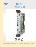
1
User Manual
User
Manual
PMC/XMC Carrier Board
Triple PMC, Dual PMC, and Dual PMC/XMC
Carrier Boards / 6RU VME64 Platform
PMC/XMC Carrier Board
Tr i p l e P M C , D u a l P M C , a n d D u a l P M C / X M C C a r r i e r B o a r d s
PMC/XMC Carrier Board
Tr i p l e P M C , D u a l P M C , a n d D u a l P M C / X M C C a r r i e r B o a r d s
PMC/XMC Carrier Board
Tr i p l e P M C , D u a l P M C , a n d D u a l P M C / X M C C a r r i e r B o a r d s
PMC/XMC Carrier Board
Tr i p l e P M C , D u a l P M C , a n d D u a l P M C / X M C C a r r i e r B o a r d s
PMC/XMC Carrier Board
Tr i p l e P M C , D u a l P M C , a n d D u a l P M C / X M C C a r r i e r B o a r d s
PMC/XMC Carrier Board
Tr i p l e P M C , D u a l P M C , a n d D u a l P M C / X M C C a r r i e r B o a r d s
PMC/XMC Carrier Board
Tr i p l e P M C , D u a l P M C , a n d D u a l P M C / X M C C a r r i e r B o a r d s
PMC/XMC Carrier Board
Tr i p l e P M C , D u a l P M C , a n d D u a l P M C / X M C C a r r i e r B o a r d s
PMC/XMC Carrier Board Manual
Version 3.0— December 2009
Themis Computer—Americas and Pacific Rim
47200 Bayside Parkway
Fremont, CA 94538
Phone (510) 252-0870
Fax (510) 490-5529
World Wide Web http://www.themis.com
Themis Computer—Rest of World
5 Rue Irene Joliot-Curie
38320 Eybens, France
Phone +33 476 14 77 80
Fax +33 476 14 77 89
Copyright © 2009 Themis Computer, Inc.
ALL RIGHTS RESERVED. No part of this publication may be reproduced in any form, by
photocopy, microfilm, retrieval system, or by any other means now known or hereafter invented without
the prior written permission of Themis Computer.
The information in this publication has been carefully checked and is believed to be accurate. However,
Themis Computer assumes no responsibility for inaccuracies. Themis Computer retains the right to
make changes to this publication at any time without prior notice. Themis Computer does not assume
any liability arising from the application or use of this publication or the product(s) described herein.
RESTRICTED RIGHTS LEGEND: Use, duplication, or disclosure by the United States Government
is subject to the restrictions set forth in DFARS 252.227-7013 (c)(1)(ii) and FAR 52.227-19.
TRADEMARKS
THEMIS® is a registered trademark of Themis Computer, Inc.
PCI Express® is a registered trademark of PCI-SIG® Special Interest Group.
All other trademarks or registered trademarks used in this publication are the property of their
respective owners.
Themis Customer Support
North America, South America, and Pacific Rim
Telephone:
Fax:
E-mail:
Web Site:
510-252-0870
510-490-5529
[email protected]
http://www.themis.com
PMC/XMC Carrier Board Manual, Version 3.0
December 2009
Part Number: 112826-020
PMC/XMC Carrier Board Manual
Version Revision History
Version 3.0................................................................................... December 2009
• Added chapter 2—entitled “2P2 PMC/XMC Carrier Board” to consolidate the
2P2 PMC/XMC Carrier Board with the 2P2 and 2P3 PMC Carrier Boards into
one manual.
• Added board weights to the appropriate specification tables.
• Assorted minor edits and changes throughout the manual.
Version 2.0.................................................................................... November 2009
Version 1.0.........................................................................................August 2006
Themis Computer
iii
PMC/XMC Carrier Board Manual
iv
Themis Computer
Table of Contents
Overview .............................................................................................................................. xiii
1. 2P2 PMC Carrier Board .............................................................................................. 1-1
1.1
2P2 PMC Carrier Board Overview ........................................................................ 1-1
1.2
Connectors ............................................................................................................. 1-4
1.2.1 2P2 PMC Carrier Board VME P1 Connector ............................................ 1-4
1.2.2 2P2 PMC Carrier Board VME P2 Connector ............................................ 1-6
1.2.3 2P2 PMC Module Slot User I/O ................................................................ 1-8
1.2.3.1 2P2 PMC Module Slot Pinouts ................................................... 1-8
1.2.4 Serial Ports TTYE and TTYF (RS232) ................................................... 1-14
1.2.5 Ethernet Port B ......................................................................................... 1-15
1.2.6 Rotary Switch .......................................................................................... 1-16
1.2.7 Stereo Audio Connectors ......................................................................... 1-16
1.3
2P2 PMC Carrier Board Solder Beads ................................................................ 1-17
1.4
Jumper Pins .......................................................................................................... 1-24
1.5
2P2 PMC Front Panel and Board Diagrams ........................................................ 1-24
1.6
2P2 PMC Carrier Board Specifications ............................................................... 1-27
1.6.1 Environmental and Compliance Requirements ....................................... 1-27
2. 2P2 PMC/XMC Carrier Board ................................................................................... 2-1
2.1
2P2 PMC/XMC Carrier Board Overview .............................................................. 2-1
2.1.1 PCI to PCI Bridge ...................................................................................... 2-4
2.1.2 The PCI Express Switch ............................................................................ 2-5
2.2
Connectors ............................................................................................................. 2-6
2.2.1 2P2 PMC/XMC Carrier Board VME P1 Connector .................................. 2-6
2.2.2 2P2 PMC/XMC Carrier Board VME P2 Connector .................................. 2-8
2.2.3 2P2 PMC/XMC Module Slots ................................................................. 2-10
2.2.3.1 PMC Module Slots .................................................................... 2-10
2.2.3.2 XMC Connectors ...................................................................... 2-15
2.2.4 Serial Ports E and F (RS232) ................................................................... 2-17
Themis Computer
v
PMC/XMC Carrier Board Manual
2.2.5 Gigabit Ethernet Port B ............................................................................ 2-18
2.2.6 Rotary Switch .......................................................................................... 2-19
2.2.7 Stereo Audio Connectors ......................................................................... 2-19
2.3
2P2 PMC/XMC Carrier Board Solder Beads ...................................................... 2-20
2.4
Switches ............................................................................................................... 2-31
2.5
Jumper Pins .......................................................................................................... 2-32
2.6
Resistor Pads ........................................................................................................ 2-32
2.7
2P2 PMC/XMC Front Panel and Board Diagrams .............................................. 2-32
2.8
2P2 PMC/XMC Carrier Board Specifications ..................................................... 2-35
2.8.1 Environmental and Compliance Requirements ....................................... 2-35
2.9
Estimated Power Requirements ........................................................................... 2-36
3. 2P3 PMC Carrier Board .............................................................................................. 3-1
3.1
2P3 PMC Carrier Board Overview ........................................................................ 3-1
3.2
Connectors ............................................................................................................. 3-4
3.2.1 2P3 PMC Carrier Board VME P1 Connector ............................................ 3-4
3.2.2 2P3 PMC Carrier Board VME P2 Connector ............................................ 3-6
3.2.3 2P3 PMC Module Slot User I/O ................................................................ 3-8
3.2.3.1 2P3 PMC Module Slot Pinouts ................................................... 3-8
3.3
2P3 PMC Carrier Board Solder Beads ................................................................ 3-14
3.4
Jumper Pins .......................................................................................................... 3-21
3.5
2P3 PMC Front Panel and Board Diagrams ........................................................ 3-21
3.6
2P3 PMC Carrier Board Specifications ............................................................... 3-24
3.6.1 Environmental and Compliance Requirements ....................................... 3-24
Appendix A. Disassembling and Reassembling Boards
(Themis USPIIe Family of Computers) ................................................... A-1
A.1 Disassembling the Boards ..................................................................................... A-2
A.2 Reassembling the Boards ...................................................................................... A-6
Index .............................................................................................................................. Index-1
Reader Comment Card
vi
Themis Computer
Table of Contents
List of Figures
Figure 1-1
2P2 PMC Carrier Board................................................................................... 1-1
Figure 1-2
2P2 PMC Carrier Board Block Diagram ......................................................... 1-2
Figure 1-3
2P2 PMC Carrier Board VME P1 Connector Pin Orientation ........................ 1-4
Figure 1-4
2P2 PMC Board VME P2 Connector Pin Orientation..................................... 1-6
Figure 1-5
2P2 PMC Module Slot Connector Pin Orientation.......................................... 1-8
Figure 1-6
Front-Panel Serial Port Pin Orientation ......................................................... 1-14
Figure 1-7
Ethernet B Connector Pin Orientation ........................................................... 1-15
Figure 1-8
Dual Stereo Audio Connector........................................................................ 1-17
Figure 1-9
2P2 PMC Carrier Board Solder-Bead Locations (Bottom Side) ................... 1-22
Figure 1-10
2P2 PMC Carrier Board Front Panel ............................................................. 1-25
Figure 1-11
2P2 PMC Carrier Board Component and Connector Diagram (Top Side) ... 1-26
Figure 2-1
2P2 PMC/XMC Carrier Board ........................................................................ 2-1
Figure 2-2
2P2 PMC/XMC Carrier Board Block Diagram ............................................... 2-2
Figure 2-3
The 2P2 PMC/XMC Module Slot Connectors (Top and Bottom Views) ....... 2-3
Figure 2-4
PCI Express Aggregation using a PCI Express Switch ................................... 2-5
Figure 2-5
2P2 PMC/XMC Carrier Board VME P1 Connector Pin Orientation .............. 2-6
Figure 2-6
2P2 PMC/XMC Board VME P2 Connector Pin Orientation .......................... 2-8
Figure 2-7
PMC Module Slot Connector Pin Orientation ............................................... 2-11
Figure 2-8
XMC Connector Pin Orientation ................................................................... 2-15
Figure 2-9
Front-Panel Serial Ports Pin Orientation ...................................................... 2-17
Figure 2-10
Gigabit Ethernet B Connector Pinout ............................................................ 2-18
Figure 2-11
Dual Stereo Audio Connector........................................................................ 2-19
Figure 2-12
2P2 PMC/XMC Carrier Board Solder-Bead, Jumper-Pin,
and Switch Locations (Top Side)
2-27
Figure 2-13
2P2 PMC/XMC Carrier Board Solder-Bead Locations (Bottom Side) ......... 2-28
Figure 2-14
2P2 PMC/XMC Carrier Board Switch Default Configurations .................... 2-31
Figure 2-15
2P2 PMC/XMC Carrier Board Front Panel ................................................... 2-33
Themis Computer
vii
PMC/XMC Carrier Board Manual
Figure 2-16
2P2 PMC/XMC Carrier Board Component and Connector Diagram ........... 2-34
Figure 3-1
2P3 PMC Carrier Board................................................................................... 3-1
Figure 3-2
2P3 PMC Carrier Board Block Diagram ......................................................... 3-2
Figure 3-3
2P3 PMC Carrier Board VME P1 Connector Orientation............................... 3-4
Figure 3-4
2P3 PMC Board VME P2 Connector Pin Orientation..................................... 3-6
Figure 3-5
2P3 PMC Module Slot Connector Pin Orientation.......................................... 3-8
Figure 3-6
2P3 PMC Carrier Board Solder-Bead Locations (Bottom Side) ................... 3-19
Figure 3-7
2P3 PMC Carrier Board Front Panel ............................................................. 3-22
Figure 3-8
2P3 PMC Carrier Board Component and Connector Diagram...................... 3-23
Figure A-1
Seven Screw Locations ................................................................................... A-2
Figure A-2
Remove 3 Screws Securing Injector/Ejector Handles .................................... A-3
Figure A-3
Hold the Baseboard Down Against Work Surface ......................................... A-4
Figure A-4
Use Fingers to Apply Upward Pressure.......................................................... A-4
Figure A-5
Separated Baseboard and PMC Carrier Board ............................................... A-5
Figure A-6
Align Three Tabs to Slots ............................................................................... A-6
Figure A-7
Expected Gap is Approximately 1/8” ............................................................. A-7
Figure A-8
Press Down on the PMC Interface Standoffs ................................................. A-8
Figure A-9
Use Interposer Material if PMC Interface Standoffs Don’t Exist .................. A-8
Figure A-10 Loctite 222MS ................................................................................................ A-9
Figure A-11 Apply Loctite to End of Screw ....................................................................... A-9
Figure A-12 Only the Last Few Threads Need Loctite ....................................................... A-9
viii
Themis Computer
Table of Contents
List of Tables
Table 1-1
2P2 PMC Carrier Board VME P1 Pinouts....................................................... 1-5
Table 1-2
2P2 PMC Carrier Board VME P2 Pinout ........................................................ 1-7
Table 1-3
2P2 PMC Carrier Slot 1 with 64 Bits of User I/O ......................................... 1-10
Table 1-4
2P2 PMC Carrier Slot 1 with 32 Bits of User I/O ......................................... 1-11
Table 1-5
2P2 PMC Carrier Slot 2 with 32 Bits of User I/O ......................................... 1-12
Table 1-6
2P2 PMC Carrier Slot 3 with 0 Bits of User I/O ........................................... 1-13
Table 1-7
Serial Ports E and F Connector Pinouts......................................................... 1-14
Table 1-8
RJ45 Ethernet B Pinout.................................................................................. 1-15
Table 1-9
2P2 PMC Carrier Board Solder-Bead Settings (Bottom Side) ...................... 1-18
Table 1-10
2P2 PMC Audio Input/Output Settings ......................................................... 1-19
Table 1-11
VME P2 Connector Configuration ................................................................ 1-20
Table 1-12
PMC Carrier Board Selection Settings .......................................................... 1-20
Table 1-13
PCB Revision Settings................................................................................... 1-20
Table 1-14
VME P2 Pin Signal Interpretation ................................................................. 1-21
Table 1-15
PMC Carrier Board VME P2 Connector SB2801–SB2832 Configuration .. 1-23
Table 1-16
Environmental Requirements ........................................................................ 1-27
Table 1-17
Compliance Requirements ............................................................................. 1-27
Table 2-1
2P2 PMC/XMC Carrier Board VME P1 Pinouts ............................................ 2-7
Table 2-2
2P2 PMC/XMC Carrier Board VME P2 Pinouts ............................................ 2-9
Table 2-3
PMC Carrier Slot 1 with 64 Bits of User I/O ................................................ 2-12
Table 2-4
PMC Carrier Slot 1 with 32 Bits of User I/O ................................................ 2-13
Table 2-5
PMC Carrier Slot 2 with 32 Bits of User I/O ................................................ 2-14
Table 2-6
XMC P15 Connector Pinouts ........................................................................ 2-16
Table 2-7
Serial Ports E and F Connector Pinouts......................................................... 2-17
Table 2-8
Gigabit Ethernet Connector-Pin Signals and LED Interpretation ................. 2-18
Table 2-9
2P2 PMC/XMC Carrier Board Solder-Bead Settings.................................... 2-20
Themis Computer
ix
PMC/XMC Carrier Board Manual
Table 2-11
VME P2 Connector Configuration ................................................................ 2-26
Table 2-12
VME P2 Pin Signal Interpretation ................................................................. 2-26
Table 2-10
2P2 PMC/XMC Audio Input/Output Settings ............................................... 2-26
Table 2-14
2P2 PMC/XMC Solder-Bead Configurations................................................ 2-29
Table 2-13
2P2 PMC/XMC VME P2 Connector SB2801–SB2832 Configuration ........ 2-30
Table 2-15
SW2 and SW3 Setting Definitions ................................................................ 2-31
Table 2-16
Environmental Requirements ........................................................................ 2-35
Table 2-17
Compliance Requirements ............................................................................. 2-35
Table 2-18
Estimated Power Requirements ..................................................................... 2-36
Table 3-1
2P3 PMC Carrier Board VME P1 Pinouts....................................................... 3-5
Table 3-2
2P3 PMC Carrier Board VME P2 Pinout ........................................................ 3-7
Table 3-3
2P3 PMC Carrier Slot 1 with 64 Bits of User I/O ......................................... 3-10
Table 3-4
2P3 PMC Carrier Slot 1 with 32 Bits of User I/O ......................................... 3-11
Table 3-5
2P3 PMC Carrier Slot 2 with 32 Bits of User I/O ......................................... 3-12
Table 3-6
2P3 PMC Carrier Slot 3 with 0 Bits of User I/O ........................................... 3-13
Table 3-7
2P3 PMC Carrier Board Solder-Bead Settings (Both Sides)......................... 3-15
Table 3-8
VME P2 Connector Configuration ................................................................ 3-16
Table 3-9
2P3 PMC Carrier Board Selection Settings ................................................... 3-17
Table 3-10
PCB Revision Settings................................................................................... 3-17
Table 3-11
VME P2 Pin Signal Interpretation ................................................................. 3-18
Table 3-12
2P3 PMC Carrier Board VME P2 Connector
SB2801–SB2832 Configuration
3-20
Table 3-13
Environmental Requirements ........................................................................ 3-24
Table 3-14
Compliance Requirements ............................................................................. 3-24
x
Themis Computer
Overview
Introduction
Thank you for purchasing the Themis PMC/XMC Carrier Board. The PMC/XMC Carrier Board is an add-on expansion board for most Themis VME single-board computers,
and supports two (on the 2P2 model) or three (on the 2P3 model) PMC and XMC (if supported) plug-in modules.
This manual describes the following three Carrier Board models:
• 2P2 PMC Carrier Board
• 2P2 PMC/XMC Carrier Board
• 2P3 PMC Carrier Board
Before you begin, carefully read each of the procedures in this manual. Serious damage can be caused by improper handling of the equipment.
Themis Computer
xi
PMC/XMC Carrier Board Manual
Carrier Board Model Configurations
Table 1 defines the Themis VME computer models that support the various carrier
boards (2P2 PMC, 2P2 PMC/XMC, or 2P3 PMC):
Table 1. Carrier Board Model Configurations
Carrier Board Supported
Model
2P2 PMC
2P2
PMC/XMCa
2P3 PMC
USPIIe
√
√
USPIIe-USB
√
√
USPIIe-Gb
√
√
USPIIIi
√
√
USPIIIi-OPT
√
√
TC2D64
√
√
TA64b
√
√
TPPC64a
√
√
TP32
√
√
a—The 2P2 PMC/XMC Carrier Board must be specifically ordered for the product to which it will be
attached (see Table 2).
b—The TA64 and TPPC64 do not support PCI Express (XMC) signaling.
Table 2. 2P2 PMC/XMC Carrier Board Part Numbers
Part Number
xii
Only Used With:
P/N 112794-001
TA64
P/N 112794-002
TPPC64
P/N 112794-004
TP32
Themis Computer
Overview
Carrier Board Model Configurations
Note: All carrier boards are shipped with VME64-type injector/ejector handles. On
special order, Triple-E-type VME ejector handles can be installed (see A and B in Figure 1). For more information on these handles, refer to the Note and Figure A-2 on
page A-3.
All multi-board systems are put together by Themis at the factory. The boards are
designed to be installed in a specific order (see the hardware manual for your system; e.g., the USPIIe-USB, USPIIIi, et al.).
A
VME64 Injector/Ejector Handle
B
Triple-E VME Ejector Handle
Figure 1. Carrier Board Handles
Do not attempt to take apart and re-order the boards in your system, without contacting Themis Support.
Caution:
Themis Computer
xiii
PMC/XMC Carrier Board Manual
Table 2 defines the interfaces supported on each carrier board.
Table 2. Carrier Board Interfaces
Interface
2 PMC Modules
2P2 PMC
2P2 PMC/XMC
√
√
2P3 PMC
√
2 XMC Modules
√
3 PMC Modules
Ethernet 10/100 Base-T
√
√
Gigabit Ethernet 10/100/1000 Base-T
Stereo Audio Line In/Line Out or
Microphone In/Headphones
√
√
Serial Ports E & F (TTYE &TTYF)
√
√
16-position Rotary-switch (user-defined)
√
√
Check Configurations
When you first receive your carrier board, confirm that the solder-bead, jumper-pin,
and switch configurations are appropriate for your application. For a complete listing of solder-bead, jumper-pin, and switch definitions, see the chapter corresponding
to your particular carrier board; i.e., 2P2 PMC, 2P2 PMC/XMC, or 2P3 PMC.
Solder-beads are set by Themis at the factory before shipping and should be changed
by Themis at the factory only.
Warning: You specify solder-bead preferences when you order your unit Since,
the solder beads are set by Themis at the factory, DO NOT ATTEMPT TO ALTER
SOLDER-BEAD CONFIGURATIONS! Attempting to alter a solder-bead configuration could seriously damage the carrier board. If you encounter a problem, contact Themis Customer Support.
xiv
Themis Computer
Overview
Check Voltage Keys
Check Voltage Keys
Each carrier board (as well as some Themis Baseboards) has two voltage-key
mounting holes: one 3.3V mounting hole and one 5V mounting hole (see the board
diagram in the chapter corresponding to your particular carrier board). Depending on
the solder bead configuration, a carrier board will support either a 3.3V or a 5V
PMC/XMC Module. A key installed in a 3.3.V hole means your carrier board is configured to accept a 3.3V module. A key installed in a 5V hole means your carrier
board is configured to accept a 5V module.
If you attempt to install a 3.3V module into a carrier board that is configured with a
5V key, the absence of a 5V hole will prevent the module from properly seating into
its connector. The same is true if you try to install a 5V module into a carrier board
that is configured with a 3.3V key. Some PMC/XMC modules will operate with
either 3.3 volts or 5 volts, in which case these “universal” modules will have two
voltage-key mounting holes, to allow the passage of either 3.3V or 5V keys.
Note: A carrier board that is configured for 3.3 volts will only accept 3.3V (or
universal) modules in any of its module slots. A carrier board that is configured
for 5 volts will only accept 5V (or universal) modules.
Intended Audience
This manual is written for Themis customers who have purchased a Themis SingleBoard Computer (e.g., USPIIe-Gb, USPIIIi, TA64, et al.), and wish to add carrierboard capability.
Unpacking
Carrier boards are factory-installed and ship already assembled to your host computer. Please refer to your system board’s hardware manual for unpacking instructions (e.g., USPIIe-Gb, USPIIIi, TA64, etc.).
In the event that a carrier board needs to be repaired or replaced, please observe the
following Caution when handling the board individually.
Themis Computer
xv
PMC/XMC Carrier Board Manual
Caution: Carrier boards contain statically sensitive components. Industry-standard
antistatic measures must be observed when removing the carrier boards from their
shipping containers and during any subsequent handling. A wrist strap provides
grounding for static electricity between your body and the chassis of the unit. Electric
current and voltage do not pass through the wrist strap.
Notes, Cautions, Warnings, and Sidebars
The following icons with accompanying formatted text are included in this document for the reasons described:
Note: A note provides additional information that may be helpful in carrying out
the procedure or action being described.
Caution: A caution describes a procedure or action that may result in damage to
the equipment. This may involve—but is not restricted to—heavy equipment or
sharp objects. To reduce the risk, follow the instructions accompanying this symbol.
Warning: A warning describes a procedure or action that may cause injury or death
to the operator. To reduce the risk, follow the instructions accompanying this symbol.
Sidebar: A “sidebar” adds detail to the section within which it is placed,
but is not absolutely vital to the description or procedure.
xvi
Themis Computer
Overview
Contact and Website Information
Contact and Website Information
Themis Computer corporate and product information may be accessed on the World
Wide Web by browsing the website at http://www.themis.com.
The Sales and Marketing Department may be reached at [email protected].
Product Warranty and Registration
Please review the Themis Computer warranty and complete the product registration
card delivered with your carrier board(s). You are not required to return the registration card to activate your product warranty; however, by registering your carrier
board, Themis Computer will be better able to provide you with timely information
updates and product-enhancement notifications.
Customer Support
Our Customer Support department is committed to providing the best product support in the computer industry. Customer support is available 8am–5pm (PST), Monday through Friday, via telephone, fax, e-mail, and our website.
If the carrier board does not behave as described, or if you encounter difficulties
installing or configuring the board, please contact customer support.
Themis Customer Support:
Telephone: +1 510-252-0870
Fax: +1 510-490-5529
E-mail: [email protected]
Website: http://www.themis.com
Themis Computer
xvii
PMC/XMC Carrier Board Manual
Your Comments are Welcome
We are interested in improving our documentation and welcome your comments and
suggestions. You can email your comments to us at [email protected] or
fill out and return the Reader Comment Card at the end of this manual. Please
include the document part number (112826-020) in the subject line of your email.
xviii
Themis Computer
1
Operation
Section
Chapter
2P2 PMC Carrier Board
1.1
2P2 PMC Carrier Board Overview
The 2P2 PCI Mezzanine Card (PMC) Carrier Board (see Figure 1-1) supports two
PMC module slots (to support vendor-specific, 32/64-bit, 33-MHz, PMC expansion
Modules) and on-board Audio/Ethernet/Serial-I/O features. Figure 1-2 on page 1-2
diagrams the functions of the 2P2 PMC Carrier Board.
The 2P2 PMC Carrier Board works in conjunction with the following Themis systems:
USPIIe, USPIIe-USB, USPIIe-Gb, USPIIIi, and USPIIIi-OPT.
Figure 1-1. 2P2 PMC Carrier Board
Themis Computer
1-1
PMC/XMC Carrier Board Manual
To Baseboard
Baseboard Connector
P0501
114 pins
PCI Bus 3
33 MHz, 64 Bit (264 MBytes/s)
Front Panel
10/100 Mbit
Ethernet B
Phyter
DP83843
Rio I/O
Controller
PCI-to-PCI
Intel 21154
SME2300
ID=4
PFCF8584
PCI Bus 4
Audio In
Audio Out
Audio
AD1881A
Slot 1
32 or 64 Bit*
64-bit PMC
Module 1
64 I/Os
ID=1 (PMC 1)
Slot 2
32 Bit*
64-bit PMC
Module 2
64 I/Os
ID=2 (PMC 2)
Rotary Switch
VME P2 Connector
Rows A & C
I 2 C Bus
33 MHz, 64 Bit (264 MBytes/s)
ID=7
(selectable on
Baseboard)
Ebus
P2702
Buffer
TTY E
RS232
TTY F
DUART
SAB82532
Flash
PROM
* I/O to VME P2 is either
all 64 bits from PMC 1
or 32 bits from PMC 1
and 32 bits from PMC 2.
Figure 1-2. 2P2 PMC Carrier Board Block Diagram
1-2
Themis Computer
1—2P2 PMC Carrier Board
2P2 PMC Carrier Board Overview
User I/O on the 2P2 PMC Carrier Board can be accessed from both the front-panel and
paddle-board connectors. In some instances, accessing a signal from one of these
access sources prevents the signal from being accessed from the second source. For
example, if TTYE is routed to the VME P2 backplane, then TTYE cannot be accessed
from the front panel.
For information regarding paddle boards, refer to your system’s hardware manual
(USPIIe, USPIIe-Gb, et al.)
Note: Some VME P2 I/O signals cannot be accessed using the available paddle
boards. You will need to provide your own connectivity, or call Themis Customer
Support for a cost estimate on building a custom Paddle Board.
Note: User I/O signals can be brought from PMC Modules in slot 1 and slot 2 to
the VME P2 connector of the 2P2 PMC Carrier Board.
A PMC Module in slot 3 has no I/O-signal access through the VME P2 connector
of the 2P2 PMC Carrier Board.
As explained further in Section 1.2.3.1 on page 1-8, user I/O on the 2P2 PMC Carrier Board can be reconfigured. For example, 64 bits of user I/O can be made available on PMC Module slot 1, presuming the user I/O on PMC Module slot 2 is not
used. On the other hand, 32 bits of user I/O can be made available on both PMC
Module slot 1 and PMC Module slot 2.
Caution: It is important to make sure that a solder-bead configuration does not
result in an unwanted change of system operational parameters. READ ALL
SOLDER-BEAD CONFIGURATION DESCRIPTIONS CAREFULLY.
(See Table 1-9 on page 1-18.)
Themis Computer
1-3
PMC/XMC Carrier Board Manual
1.2
Connectors
The 2P2 PMC Carrier Board provides two PMC module slots and the following
input/output from its front panel:
• Ethernet port B (10/100 Base-T)
• Audio Line-in or Mic-in
• Audio Line-out or Headphone Out
• User-defined 16-position Rotary Switch
• Serial (TTY) port E ......................................................................................................RS232
• Serial (TTY) port F .....................................................................................................RS232
• PMC Module slot 1
• PMC Module slot 2
Attach adapter cables to the appropriate front panel and VME P2 Paddle Board connectors on the 2P2 PMC Carrier Board. The following sections provide detailed
information about the Carrier Board connectors.
1.2.1
2P2 PMC Carrier Board VME P1 Connector
The VME P1 connector provides daisy-chaining of IACK and BG signals. There is
no need to jumper those signals manually for the position occupied by the 2P2 PMC
Carrier Board. See Table 1-1 on page 1-5 for the VME P1 connector pinouts.
The VME P1 interface employs a standard 3-row VME connector. Figure 1-3 shows
the pin orientation for the VME P1 connector.
(Top View)
PCB Edge
Row A
Row B
Row C
1
32
Figure 1-3. 2P2 PMC Carrier Board VME P1 Connector Pin Orientation
1-4
Themis Computer
1—2P2 PMC Carrier Board
Connectors
Table 1-1. 2P2 PMC Carrier Board VME P1 Pinouts
Pin
Row A
Signal Name
Row B
Signal Name
Row C
Signal Name
1
NC
NC
NC
2
NC
NC
NC
3
NC
NC
NC
4
NC
DAISY_CHAIN_BGIN_L<0>
NC
5
NC
DAISY_CHAIN_BGOUT_L<0>
NC
6
NC
DAISY_CHAIN_BGIN_L<1>
NC
7
NC
DAISY_CHAIN_BGOUT_L<1>
NC
8
NC
DAISY_CHAIN_BGIN_L<2>
NC
9
GND
DAISY_CHAIN_BGOUT_L<2>
GND
10
NC
DAISY_CHAIN_BGIN_L<3>
NC
11
GND
DAISY_CHAIN_BGOUT_L<3>
NC
12
NC
NC
NC
13
NC
NC
NC
14
NC
NC
NC
15
GND
NC
NC
16
NC
NC
NC
17
GND
NC
NC
18
NC
NC
NC
19
GND
NC
NC
20
NC
GND
NC
21
DAISY_CHAIN_IACKIN_L
NC
NC
22
DAISY_CHAIN_IACKOUT_L
NC
NC
23
NC
GND
NC
24
NC
NC
NC
25
NC
NC
NC
26
NC
NC
NC
27
NC
NC
NC
28
NC
NC
NC
29
NC
NC
NC
30
NC
NC
NC
31
-12V
NC
+12V
32
VCC
VCC
VCC
Themis Computer
1-5
PMC/XMC Carrier Board Manual
1.2.2
2P2 PMC Carrier Board VME P2 Connector
The VME P2 connector of the 2P2 PMC Carrier Board transmits 64 user-defined
signals through rows A and C, all from a combination of signals (solder-bead
switchable) from PMC Module slots 1 and 2, Serial Ports E (TTY E) and F (TTY F),
the front-panel User Rotary Switch, and the I2C bus (see Table 1-15 on page 1-23 for
details). See Table 1-2 on page 1-7 for the VME P2 connector pinouts.
The VME P2 interface employs a standard 3-row VME connector. Figure 1-4 shows
the pin orientation for the VME P2 connector.
(Top View)
PCB Edge
Row A
Row B
Row C
1
32
Figure 1-4. 2P2 PMC Board VME P2 Connector Pin Orientation
1-6
Themis Computer
1—2P2 PMC Carrier Board
Connectors
Table 1-2. 2P2 PMC Carrier Board VME P2 Pinout
Pin
Row A
Signal Name
Row B
Signal Name
Row C
Signal Name
1
User-switchablea
VCC
User-switchablea
2
User-switchablea
GND
User-switchablea
3
User-switchablea
NC
User-switchablea
4
User-switchablea
NC
User-switchablea
5
User-switchablea
NC
User-switchablea
6
User-switchablea
NC
User-switchablea
7
User-switchablea
NC
User-switchablea
8
User-switchablea
NC
User-switchablea
9
User-switchablea
NC
User-switchablea
10
User-switchablea
NC
User-switchablea
11
User-switchablea
NC
User-switchablea
12
User-switchablea
NC
User-switchablea
13
User-switchablea
NC
User-switchablea
14
User-switchablea
NC
User-switchablea
15
User-switchablea
NC
User-switchablea
16
User-switchablea
NC
User-switchablea
17
PMC1_IO34
NC
PMC1_IO33
18
PMC1_IO36
NC
PMC1_IO35
19
PMC1_IO38
NC
PMC1_IO37
20
PMC1_IO40
NC
PMC1_IO39
21
PMC1_IO42
NC
PMC1_IO41
22
PMC1_IO44
GND
PMC1_IO43
23
PMC1_IO46
NC
PMC1_IO45
24
PMC1_IO48
NC
PMC1_IO47
25
PMC1_IO50
NC
PMC1_IO49
26
PMC1_IO52
NC
PMC1_IO51
27
PMC1_IO54
NC
PMC1_IO53
28
PMC1_IO56
NC
PMC1_IO55
29
PMC1_IO58
NC
PMC1_IO57
30
PMC1_IO60
NC
PMC1_IO59
31
PMC1_IO62
GND
PMC1_IO61
32
PMC1_IO64
VCC
PMC1_IO63
a—See Table 1-15 on page 1-23.
Themis Computer
1-7
PMC/XMC Carrier Board Manual
1.2.3
2P2 PMC Module Slot User I/O
In addition to the standard PMC I/O, 64 bits of configurable user I/O are provided
from the VME P2 connector directly to the PMC 1 and PMC 2 Module slot positions. All 64 bits may be routed to PMC 1, leaving 0 bits of user I/O for PMC 2.
Alternatively, 32 bits may be routed to PMC 1 and 32 bits to PMC 2. In the latter
case, PMC 1 will utilize the upper VME P2 signals—VME P2 A[32..17] and VME
P2 C[32..17]—while PMC 2 will utilize the lower VME P2 signals—VME P2
A[16..1] and VME P2 C[16..1]. The signals are available on the J1004 connector of
PMC slot 1 and the J1104 connector of PMC slot 2. If all 64 bits of user I/O are
routed to PMC slot 1, it utilizes all 64 signals of the VME P2 connector. In this case,
all 64 signals are available on the J1004 connector of PMC slot 1.
Note: User I/O is directed to PMC 1 and PMC 2 Modules through solder-bead
configurations (see Table 1-9 on page 1-18).
1.2.3.1 2P2 PMC Module Slot Pinouts
This section provides the pinouts of the 64 PMC User I/O signals that can be brought from
PMC Module Slot 1 and Slot 2 to the VME P2 connector of the 2P2 PMC Carrier Board.
Figure 1-5 shows the pin orientation of the 2P2 PMC Module Slot connector used to
install PMC Modules onto the top side of the circuit board (USPIIe, USPIIe-USB,
USPIIe-Gb, USPIIIi, or USPIIIi-OPT).
• Connector Type: 64-Pin, Female, 10mm, Dual Row
• Manufacturer; Part Number: AMP; 120528-1
63
1
64
2
Figure 1-5. 2P2 PMC Module Slot Connector Pin Orientation
1-8
Themis Computer
1—2P2 PMC Carrier Board
Connectors
As seen in Table 1-11 on page 1-20, three solder-bead-selectable configurations are
possible:
Themis Computer
•
64 user signals from PMC Slot 1 (through J1004; see Table 1-3, page 1-10),
and none from PMC Module Slot 2.
•
32 user signals from PMC Module Slot 1 (through J1004; see Table 1-4,
page 1-11), and the following I/O signals: Serial Ports E and F, I2C, and
User-Programmable Rotary Switch (see Table 1-15, page 1-23).
This is the default configuration.
•
32 user signals from PMC Module Slot 1 (through J1004; see Table 1-4,
page 1-11) and 32 user signals from PMC Module Slot 2 (through J1104; see
Table 1-5, page 1-12).
1-9
PMC/XMC Carrier Board Manual
Table 1-3. 2P2 PMC Carrier Slot 1 with 64 Bits of User I/O
1-10
PMC Pin (J1004)
VME P2 Signal
PMC Pin (J1004)
VME P2 Signal
1
PMC IO C1
2
PMC IO A1
3
PMC IO C2
4
PMC IO A2
5
PMC IO C3
6
PMC IO A3
7
PMC IO C4
8
PMC IO A4
9
PMC IO C5
10
PMC IO A5
11
PMC IO C6
12
PMC IO A6
13
PMC IO C7
14
PMC IO A7
15
PMC IO C8
16
PMC IO A8
17
PMC IO C9
18
PMC IO A9
19
PMC IO C10
20
PMC IO A10
21
PMC IO C11
22
PMC IO A11
23
PMC IO C12
24
PMC IO A12
25
PMC IO C13
26
PMC IO A13
27
PMC IO C14
28
PMC IO A14
29
PMC IO C15
30
PMC IO A15
31
PMC IO C16
32
PMC IO A16
33
PMC IO C17
34
PMC IO A17
35
PMC IO C18
36
PMC IO A18
37
PMC IO C19
38
PMC IO A19
39
PMC IO C20
40
PMC IO A20
41
PMC IO C21
42
PMC IO A21
43
PMC IO C22
44
PMC IO A22
45
PMC IO C23
46
PMC IO A23
47
PMC IO C24
48
PMC IO A24
49
PMC IO C25
50
PMC IO A25
51
PMC IO C26
52
PMC IO A26
53
PMC IO C27
54
PMC IO A27
55
PMC IO C28
56
PMC IO A28
57
PMC IO C29
58
PMC IO A29
59
PMC IO C30
60
PMC IO A30
61
PMC IO C31
62
PMC IO A31
63
PMC IO C32
64
PMC IO A32
Themis Computer
1—2P2 PMC Carrier Board
Connectors
Table 1-4. 2P2 PMC Carrier Slot 1 with 32 Bits of User I/O
PMC Pin (J1004)
VME P2 Signal
PMC Pin (J1004)
VME P2 Signal
1
NC
2
NC
3
NC
4
NC
5
NC
6
NC
7
NC
8
NC
9
NC
10
NC
11
NC
12
NC
13
NC
14
NC
15
NC
16
NC
17
NC
18
NC
19
NC
20
NC
21
NC
22
NC
23
NC
24
NC
25
NC
26
NC
27
NC
28
NC
29
NC
30
NC
31
NC
32
NC
33
PMC IO C17
34
PMC IO A17
35
PMC IO C18
36
PMC IO A18
37
PMC IO C19
38
PMC IO A19
39
PMC IO C20
40
PMC IO A20
41
PMC IO C21
42
PMC IO A21
43
PMC IO C22
44
PMC IO A22
45
PMC IO C23
46
PMC IO A23
47
PMC IO C24
48
PMC IO A24
49
PMC IO C25
50
PMC IO A25
51
PMC IO C26
52
PMC IO A26
53
PMC IO C27
54
PMC IO A27
55
PMC IO C28
56
PMC IO A28
57
PMC IO C29
58
PMC IO A29
59
PMC IO C30
60
PMC IO A30
61
PMC IO C31
62
PMC IO A31
63
PMC IO C32
64
PMC IO A32
Themis Computer
1-11
PMC/XMC Carrier Board Manual
Table 1-5. 2P2 PMC Carrier Slot 2 with 32 Bits of User I/O
1-12
PMC Pin (J1104)
VME P2 Signal
PMC Pin (J1104)
VME P2 Signal
1
NC
2
NC
3
NC
4
NC
5
NC
6
NC
7
NC
8
NC
9
NC
10
NC
11
NC
12
NC
13
NC
14
NC
15
NC
16
NC
17
NC
18
NC
19
NC
20
NC
21
NC
22
NC
23
NC
24
NC
25
NC
26
NC
27
NC
28
NC
29
NC
30
NC
31
NC
32
NC
33
PMC IO C1
34
PMC IO A1
35
PMC IO C2
36
PMC IO A2
37
PMC IO C3
38
PMC IO A3
39
PMC IO C4
40
PMC IO A4
41
PMC IO C5
42
PMC IO A5
43
PMC IO C6
44
PMC IO A6
45
PMC IO C7
46
PMC IO A7
47
PMC IO C8
48
PMC IO A8
49
PMC IO C9
50
PMC IO A9
51
PMC IO C10
52
PMC IO A10
53
PMC IO C11
54
PMC IO A11
55
PMC IO C12
56
PMC IO A12
57
PMC IO C13
58
PMC IO A13
59
PMC IO C14
60
PMC IO A14
61
PMC IO C15
62
PMC IO A15
63
PMC IO C16
64
PMC IO A16
Themis Computer
1—2P2 PMC Carrier Board
Connectors
Table 1-6. 2P2 PMC Carrier Slot 3 with 0 Bits of User I/O
PMC Pin (J1204)
VME P2 Signal
PMC Pin (J1204)
VME P2 Signal
1
Not available
2
Not available
3
Not available
4
Not available
5
Not available
6
Not available
7
Not available
8
Not available
9
Not available
10
Not available
11
Not available
12
Not available
13
Not available
14
Not available
15
Not available
16
Not available
17
Not available
18
Not available
19
Not available
20
Not available
21
Not available
22
Not available
23
Not available
24
Not available
25
Not available
26
Not available
27
Not available
28
Not available
29
Not available
30
Not available
31
Not available
32
Not available
33
Not available
34
Not available
35
Not available
36
Not available
37
Not available
38
Not available
39
Not available
40
Not available
41
Not available
42
Not available
43
Not available
44
Not available
45
Not available
46
Not available
47
Not available
48
Not available
49
Not available
50
Not available
51
Not available
52
Not available
53
Not available
54
Not available
55
Not available
56
Not available
57
Not available
58
Not available
59
Not available
60
Not available
61
Not available
62
Not available
63
Not available
64
Not available
Themis Computer
1-13
PMC/XMC Carrier Board Manual
1.2.4
Serial Ports TTYE and TTYF (RS232)
There are two serial port connections available from the front panel of the 2P2 PMC
Carrier Board or from the 2P2 PMC Carrier Board VME P2 bus. They are Serial Port
E (TTYE—RS232) and Serial Port F (TTYF—RS232). These serial ports are supported by the Siemens SAB82532 DUART serial controller, located on the 2P2 PMC
Carrier Board. Figure 1-6 shows the pin orientation of the serial port connectors.
Use the following connector type to connect to the 2P2 PMC serial ports:
• Connector Type: Dual-stacked 9-pin Micro-D
• Part Number: ITT Cannon MDSM-18PE-Z10-VR25
• Themis Cable (optional): 108113
1
6
9
5
Figure 1-6. Front-Panel Serial Port Pin Orientation
Table 1-7. Serial Ports E and F Connector Pinouts
Carrier Board
is marked:
B1
Port E
Pina
Signal Name
TTY E
Signal
1
DCD
2
RD
3
TD
4
DTR
B5
5
SIG GND
B6
6
DSR
7
B9
Description
Data Carrier Detect
TTY F
Signal
Port F
Pina
Carrier Board
is marked:
DCD
1
Receive Data
RD
2
Transmit Data
TD
3
DTR
4
SIG GND
5
A5
Data Set Ready
DSR
6
A6
RTS
Request to Send
RTS
7
8
CTS
Clear to Send
CTS
8
9
RI
Ring indicator
RI
9
Data Terminal Ready
Signal Ground
A1
A9
a—Important: The A and B associated with Serial Port connector pins on PC boards are interpreted as follows: Port E pins
are marked with a B. Port F pins are marked with an A.
1-14
Themis Computer
1—2P2 PMC Carrier Board
Connectors
1.2.5
Ethernet Port B
The 2P2 PMC Carrier Board features an RJ45 port on the Front Panel for 10/100 Base-T
Ethernet connection.
In units where only the Baseboard is present, a single network connection
(Ethernet A) is available through the RJ45 connector. With the addition of a 2P2
PMC Carrier Board, a second network connection (Ethernet B) is available through
the carrier board front panel. Both Ethernet A and B may be active simultaneously.
After attaching the 2P2 PMC Carrier Board to a network, you can verify proper
physical connection by executing the OBP network selftest (test net). This test
will indicate external loopback failure on each of the network interfaces when there
is not a proper physical connection.
Use the following connector to attach to the 2P2 PMC Ethernet port:
• Connector Type: RJ45 TPE
• Connector Part Number: AMP 406549-1
Figure 1-8 shows the pin orientation of the Ethernet B connector.
Speed LED
8
Link Status LED
1
Figure 1-7. Ethernet B Connector Pin Orientation
Table 1-8. RJ45 Ethernet B Pinout
Themis Computer
Pin
Signal Name
1
TXD+
2
TXD-
3
RXD+
4
4T_D3P
5
4T_D3P
6
RXD-
7
4T_D4P
8
4T_D4P
1-15
PMC/XMC Carrier Board Manual
1.2.6
Rotary Switch
The 2P2 PMC Carrier Board provides a 16-position Rotary Switch that is connected
to the Coolrunner Complex Programmable Logic Device (CPLD). This switch
allows you to change the switch position from the 2P2 PMC Carrier Board front
panel. The 16 positions correspond to 16 user-defined meanings.
Depending on the solder bead settings, the rotary switch position may also be presented as a binary value on VME P2 connector pins A2 through A5. Refer to
Table 1-15 on page 1-23 for details.
Note: OBP records the value of the user-defined Rotary Switch as an OBP environment variable called themis-switch-value. The default value for this
variable is 255 (0xff), which is assigned if the 2P2 PMC Carrier Board is not connected. If the board is connected, a value from 0 through 15 is assigned.
To find the value of the switch setting from OBP, type:
ok printenv themis-switch-value
To find the value of the switch setting from Solaris, type:
# prtconf -vp | grep themis
1.2.7
Stereo Audio Connectors
The 2P2 PMC Carrier Board provides audio input and output via two audio jacks on
the board’s front panel.
The audio jacks (shown in Figure 1-8) can be configured to provide one of two I/O
options, depending on the setting of particular solder beads on the 2P2 PMC board
(see Table 1-9 on page 1-18 and Table 1-10 on page 1-19 for Audio I/O solder bead
settings). You specify solder-bead preferences when you order your unit. You may
chose to have the 2P2 PMC board configured with one of following options:
•
Line In/Line Out
•
MIC In/Headphone Out
Warning: Solder beads are set by Themis at the factory. DO NOT ATTEMPT TO
ALTER SOLDER-BEAD CONFIGURATIONS! Attempting to alter a solder-bead
configuration could seriously damage the carrier boards. If you encounter a problem, contact Themis Customer Support.
1-16
Themis Computer
1—2P2 PMC Carrier Board
2P2 PMC Carrier Board Solder Beads
Use the following connector type to attach to the 2P2 PMC Audio ports:
• Connector Type: Industry-standard 1/8″ Mini Stereo Jack
• Connector Part Number: ASTRON AT-JY3540-050B
In Jack
Out Jack
Front View
Figure 1-8. Dual Stereo Audio Connector
1.3
2P2 PMC Carrier Board Solder Beads
Solder beads are found only on the bottom side of the 2P2 PMC Carrier Board and
are described in Table 1-9.
In Table 1-9, if no pad number is given, only 2 solder pads exist. If there are 3 or
more solder pads, the two pads listed are shorted together. Short means a solder
bead is installed, creating an electrical path between contacts. Open means a solder
bead is not installed, hence the path between the contacts is open.
Figure 1-9 on page 1-22, provides the location of the 2P2 PMC Carrier Board solder beads.
Remember that pad 1 is indicated on the board by a dot and/or a thick bar line.
Caution: When dealing with a 3- or 4-pad solder-bead switch, a solder bead will
short only one set of pads.
If a solder bead shorts more than 2 pads, call Themis Customer Support.
Caution: It is important to make sure that a solder-bead configuration does not
result in an unwanted change of system operational parameters. READ ALL
SOLDER-BEAD CONFIGURATION DESCRIPTIONS CAREFULLY. (See
Table 1-9 on page 1-18.)
Themis Computer
1-17
PMC/XMC Carrier Board Manual
Table 1-9. 2P2 PMC Carrier Board Solder-Bead Settings (Bottom Side)
Solder
Bead
Settinga
Short 1–2
Required when the 2P2 PMC Carrier Board (in the second VME slot) is directly
connected to the Baseboard
Short 2–3
Required when the 2P2 PMC Carrier Board (in the third VME slot) is directly connected to the Graphics Board or the PMC Carrier Board in the second VME slot
Short 1–2
Normal operation
Short 2–3
For engineering use only
Short 1–2
Required when the 2P2 PMC Carrier Board supports 5V VIO PMC modules
Short 2–3
Required when the 2P2 PMC Carrier Board supports 3.3V VIO PMC modules
Short 1–2
Set Rio to Motherboard mode (2P2 PMC Carrier Board must be set to this mode)
Short 2–3
Set Rio to Add-In mode (factory use only)
Short
Assign Ethernet interrupt to PCI interrupt
Open
Block Ethernet interrupt (factory use only)
Short
Disable 5-MHz I2C clock
Open
Enable 5-MHz I2C clock
Short
Audio interface configuration (see Table 1-10, page 1-19); 2P2 PMC Carrier
Board model 2P2 only
SB0901
SB0902
SB0903
SB1301
SB1302
SB1801
SB1802
SB1803
Open
Short
Open
SB1804
SB2403
and
SB2404
SB2407
and
SB2408
SB2801
to
SB2832
SB2833
Description
Audio interface configuration (see Table 1-10, page 1-19); 2P2 PMC Carrier
Board model 2P2 only
Not used
Short 1–2
Short 2–3
Short 1–2
Short 2–3
Audio interface configuration (see Table 1-10, page 1-19); 2P2 PMC Carrier
Board model 2P2 only
Audio interface configuration (see Table 1-10, page 1-19); 2P2 PMC Carrier
Board model 2P2 only
Short 1–4
Short 2–4
VME P2 connector pinout configuration (see Table 1-11, page 1-20)
Short 3–4
Short
Open
Board type selection (see Table 1-12, page 1-20)
Note: Footnotes are described at the end of Table 1-9 on page 1-19.
1-18
Themis Computer
1—2P2 PMC Carrier Board
2P2 PMC Carrier Board Solder Beads
Table 1-9. 2P2 PMC Carrier Board Solder-Bead Settings (Bottom Side) (Continued)
Solder
Bead
SB2834
SB2835
SB2836
SB2837
SB2838
SB2839
SB2840
SB3002
SB3003
Settinga
Short
Open
Short
Open
Short
Open
Short
Open
Short
Open
Short
Open
Short
Open
Description
PCB Revision settings indicator (see Table 1-13, page 1-20)
VME P2 connector pinout configuration (see Table 1-11, page 1-20)
VME P2 connector pinout configuration (see Table 1-11, page 1-20)
PCB Revision settings indicator (see Table 1-13, page 1-20)
PCB Revision settings indicator (see Table 1-13, page 1-20)
Board type selection (see Table 1-12, page 1-20)
Board type selection (see Table 1-12, page 1-20)
Short
Flash PROM selected is writable
Open
Flash PROM selected is not writable
Short 1–2
Enable 5V Flash programming voltage (Vpp)
Short 2–3
Enable 12V Flash programming voltage (Vpp)
a—Boldface = the default solder-bead position. No boldface indicates there is no default.
Table 1-10. 2P2 PMC Audio Input/Output Settings
Solder Bead
Line In
SB1802
Open
Microphone
In
Headphones
Short
SB1803
Open
Short
SB2403 and SB2404
Short 2–3
Short 1–2
SB2407 and SB2408
Themis Computer
Line Out
Short 2–3
Short 1–2
1-19
PMC/XMC Carrier Board Manual
Table 1-11. VME P2 Connector Configurationa
SB2801 to
SB2832
SB2835
SB2836
All PMC 1
Short 1–4
Short
Short
PMC 1 (16 pins) and PMC 2 (16 pins)
Short 3–4
Open
Short
PMC 1 (16 pins) and PMC Carrier I/O
Short 2–4
Definition (32 Pins)
Open
a—See Table 1-14, page 1-21, and Table 1-15, page 1-23, for details. Dark shaded area indicates no preference.
Table 1-12. PMC Carrier Board Selection Settings
2 PMCs in first I/O slot (VME card n)
a
SB2839
SB2840
SB2833
Short
Short
Short
3 PMCs in first I/O slot (VME card n)
Reserved for 2P3 PMC Carrier Board.
2 PMCs in second I/O slot (VME card n+1)
Short
3 PMCs in second I/O slot (VME card n+1)
Reserved for 2P3 PMC Carrier Board.
Reserved
Open
Short
Short
Reserved
Open
Short
Open
Reserved
Open
Open
Short
Reserved
Open
Open
Open
Open
Short
a—For the USPIIe family of computers, n = 2
For single-CPU USPIIIi, n = 3
For dual-CPU USPIIIi, n = 4
Table 1-13. PCB Revision Settings
1-20
Revision
SB2834
SB2837
SB2838
A
Short
Short
Short
B
Short
Short
Open
C
Short
Open
Short
D
Short
Open
Open
E
Open
Short
Short
F
Open
Short
Open
Y
Open
Open
Short
X
Open
Open
Open
Themis Computer
1—2P2 PMC Carrier Board
2P2 PMC Carrier Board Solder Beads
In Table 1-15 on page 1-23, VME P2 pin signals are interpreted as follows:
Table 1-14. VME P2 Pin Signal Interpretation
Signal
Interpretation
PMC1_IOn
The nth pin of PMC Module slot 1
PMC2_IOn
The nth pin of PMC Module slot 2
USR_SW1_n
The User Switch is equal to the value n (1, 2, 4, or 8)
SSER_E_xyz
The xyz signal of Serial Port E
SSER_F_xyz
The xyz signal of Serial Port F
I2C_abc_xyz
An I2C bus signal (1.5A, Vcc Polyswitch fuse)
The bold lines in Table 1-15 outline the various functions available from the VME P2 connector according to the PMC Carrier Board solder-bead configuration, namely:
Themis Computer
•
PMC Module slot 1
•
PMC Module slot 2
•
Serial Port E
•
Serial Port F
•
User Switch
•
I2C-bus signals
1-21
PMC/XMC Carrier Board Manual
SB2408
SB1301
SB1302
SB2407
SB2403
SB2404
SB1802
VME P1
3
= Actual location
of solder beads
SB2836 SB2834
= Description
of solder beads
= May be set open or short
as per manufacturing.
SB2817
SB2818
SB2820
SB2822
SB2824
SB2826
SB2804
SB2819
SB2821
SB2823
SB2825
SB2827
SB2828
SB2830
Solder short,
pads 2 & 3
SB2832
2
SB2829
3
1
SB2831
2
SB2814
4
Thick bar = Pad 1
SB2816
1
SB2813
Legend
VME P2
SB0903
SB2815
SB2811
SB2809
SB2807
SB0902
SB2806
SB2805
SB0901
SB2808
SB2803
SB3002
SB2810
SB3003
SB2802
SB1803
SB2812
SB1801
SB2801
SB1804
SB2840 SB2838
SB2835 SB2833
SB2839 SB2837
Figure 1-9. 2P2 PMC Carrier Board Solder-Bead Locations (Bottom Side)
1-22
Themis Computer
1—2P2 PMC Carrier Board
2P2 PMC Carrier Board Solder Beads
Table 1-15. PMC Carrier Board VME P2 Connector SB2801–SB2832 Configuration a
VME P2 Connector Row Ab
VME P2 Connector Row Cb
Pin
Pin Signal
with SB 1–4
Shorted
Pin Signal
with SB 2–4
Shorted
Pin Signal
with SB 3–4
Shorted
Pin
Pin Signal
with SB 1–4
Shorted
Pin Signal
with SB 2–4
Shorted
Pin Signal
with SB 3–4
Shorted
A1
PMC1_IO2
Ground
PMC2_IO34
C1
PMC1_IO1
Ground
PMC2_IO33
A2
PMC1_IO4
USR_SW1_8
PMC2_IO36
C2
PMC1_IO3
I2C_CON_SDA
PMC2_IO35
A3
PMC1_IO6
USR_SW1_4
PMC2_IO38
C3
PMC1_IO5
I2C_CON_SCL
PMC2_IO37
A4
PMC1_IO8
USR_SW1_2
PMC2_IO40
C4
PMC1_IO7
Ground
PMC2_IO39
A5
PMC1_IO10
USR_SW1_1
PMC2_IO42
C5
PMC1_IO9
I2C_BUF_VCC
PMC2_IO41
A6
PMC1_IO12
Ground
PMC2_IO44
C6
PMC1_IO11
—
PMC2_IO43
A7
PMC1_IO14
—
PMC2_IO46
C7
PMC1_IO13
—
PMC2_IO45
A8
PMC1_IO16
—
PMC2_IO48
C8
PMC1_IO15
—
PMC2_IO47
A9
PMC1_IO18
SSER_E_TXD
PMC2_IO50
C9
PMC1_IO17
SSER_F_TXD
PMC2_IO49
A10
PMC1_IO20
SSER_E_RXD
PMC2_IO52
C10
PMC1_IO19
SSER_F_RXD
PMC2_IO51
A11
PMC1_IO22
SSER_E_CTS
PMC2_IO54
C11
PMC1_IO21
SSER_F_CTS
PMC2_IO53
A12
PMC1_IO24
SSER_E_RTS
PMC2_IO56
C12
PMC1_IO23
SSER_F_RTS
PMC2_IO55
A13
PMC1_IO26
SSER_E_DTR
PMC2_IO58
C13
PMC1_IO25
SSER_F_DTR
PMC2_IO57
A14
PMC1_IO28
SSER_E_DCD
PMC2_IO60
C14
PMC1_IO27
SSER_F_DCD
PMC2_IO59
A15
PMC1_IO30
SSER_E_DSR
PMC2_IO62
C15
PMC1_IO29
SSER_F_DSR
PMC2_IO61
A16
PMC1_IO32
SSER_E_RI
PMC2_IO64
C16
PMC1_IO31
SSER_F_RI
PMC2_IO63
A17
PMC1_IO34
C17
PMC1_IO33
A18
PMC1_IO36
C18
PMC1_IO35
A19
PMC1_IO38
C19
PMC1_IO37
A20
PMC1_IO40
C20
PMC1_IO39
A21
PMC1_IO42
C21
PMC1_IO41
A22
PMC1_IO44
C22
PMC1_IO43
A23
PMC1_IO46
C23
PMC1_IO45
A24
PMC1_IO48
C24
PMC1_IO47
A25
PMC1_IO50
C25
PMC1_IO49
A26
PMC1_IO52
C26
PMC1_IO51
A27
PMC1_IO54
C27
PMC1_IO53
A28
PMC1_IO56
C28
PMC1_IO55
A29
PMC1_IO58
C29
PMC1_IO57
Note: Footnotes are described at the end of Table 1-15 on page 1-24.
Themis Computer
1-23
PMC/XMC Carrier Board Manual
Table 1-15. PMC Carrier Board VME P2 Connector SB2801–SB2832 Configuration (Continued)a
VME P2 Connector Row Ab
Pin
Pin Signal
with SB 1–4
Shorted
Pin Signal
with SB 2–4
Shorted
Pin Signal
with SB 3–4
Shorted
VME P2 Connector Row Cb
Pin
Pin Signal
with SB 1–4
Shorted
Pin Signal
with SB 2–4
Shorted
A30
PMC1_IO60
C30
PMC1_IO59
A31
PMC1_IO62
C31
PMC1_IO61
A32
PMC1_IO64
C32
PMC1_IO63
Pin Signal
with SB 3–4
Shorted
a—Bold lines outline the various functions available from the VME P2 connector, as defined on page 1-21.
b—See Table 1-2 on page 1-7.
1.4
Jumper Pins
There are no jumper pins on the 2P2 PMC Carrier Board.
1.5
2P2 PMC Front Panel and Board Diagrams
This section’s front panel and board diagrams provide component and connector
information at a glance.
Figure 1-10 on page 1-25 shows the 2P2 PMC front panel.
Figure 1-11 on page 1-26 shows the 2P2 PMC components and connectors.
1-24
Themis Computer
1—2P2 PMC Carrier Board
2P2 PMC Front Panel and Board Diagrams
63'
(7+(51(7 %
/1.
A
U
D
I
O
Gigabit Ethernet B
Line-In / Mic-In *
Line-Out / Headphones-Out *
IN
OUT
User-defined Rotary Switch
0
C
4
8
Serial E
T
T
Y
T
T
Y
E
F
Serial F
PMC Module 2
30&
PMC Module 1
30&
* Line In/Out and Mic/Headphones
are switchable through
on-board solder beads.
See Table 1-10.
Figure 1-10. 2P2 PMC Carrier Board Front Panel
Themis Computer
1-25
PMC/XMC Carrier Board Manual
P2601
Ethernet B
Phyter
Sun Rio
Ethernet
Controller
(DP83843)
U1501
Audio In
(STP2003)
U1301
Audio Out
VME P1
Rotary Switch
Serial Port E
Audio
PMC Carrier
Board Mating
Connectors
(underneath
on bottom
side)}only 1
installed
depending
on slot
location*
(AD1881A)
U1901
Serial Port F
DUART
Serial
Controller
U2301
PMC Module
Serial E
(SAB82532/QFP)
Serial F
P0602
FLASH
PROM
U3003
Secondary
PCI-to-PCI
Bridge
P0501
P2702
(Intel 21154)
(28F032SA_TSOP)
5V PMC
Module
Lock-out Key
U0901
PMC Module
VME P2
3.3V PMC
Module
Lock-out Key
Themis
PLD
U1401
Component Side
* P0501 connects to the
PMC Module Outline
Baseboard; P0602 is
not presently used.
Figure 1-11. 2P2 PMC Carrier Board Component and Connector Diagram (Top Side)
1-26
Themis Computer
1—2P2 PMC Carrier Board
2P2 PMC Carrier Board Specifications
1.6
2P2 PMC Carrier Board Specifications
1.6.1
Environmental and Compliance Requirements
The 2P2 PMC Carrier Board meets the environmental and compliance regulatory
requirements defined in Tables 1-16 and 1-17.
Table 1-16. Environmental Requirements
Parameter
Operating
Non-Operating
Weight
0.70 pounds
NA
Temperature
0–55° C
0–80° C
Humidity
0–95%
N/A
Altitude
0–10,000’
0–30,000’
Shock
30G
30G
Vibration
10Hz–2kHz
10Hz–2kHz
Airflow
300 LFM min.
N/A
Table 1-17. Compliance Requirements
Parameter
Specifications
Radiated and Conducted Emissions
FCC Class A
PCB FAB Material
FR-408 or equivalent
PCB FAB Thickness
0.062”
Themis Computer
1-27
PMC/XMC Carrier Board Manual
1-28
Themis Computer
2
Operation
Section
Chapter
2P2 PMC/XMC Carrier Board
2.1
2P2 PMC/XMC Carrier Board Overview
The 2P2 PMC/Switched Mezzanine Card (XMC) Carrier Board (Figure 2-1) supports a combination of two PMC Module slots (to support user-specified, 32/64-bit,
66-MHz and/or PCI Express XMC/PMC expansion Modules) and two XMC Module slots (see Figure 2-3 on page 2-3), on-board Audio/Ethernet/Serial-I/O features,
as well as x4 PCI Express per PMC/XMC module. (See Table 1 on page xii for a list
of processor boards that support XMC modules.)
Figure 2-2 on page 2-2 diagrams the functions of the 2P2 PMC/XMC Carrier Board.
The 2P2 PMC/XMC Carrier Board works in conjunction with the following Themis
systems: TC2D64, TA64, TPPC64, and TP32. Please note that the TA64 and TPPC64
do not support PCI Express (XMC) signaling.
Figure 2-1. 2P2 PMC/XMC Carrier Board
Themis Computer
2-1
PMC/XMC Carrier Board Manual
Mictor PCI-E
I2C/SMBus
PCI Express
from Baseboard
PCI Express 8 Lane
PCI Express
Switch
(PEX8516)
Mictor - baseboard
Mictor - Graphics
Mictor - 2P3
AC97 DI/O, CLK
64 bit PCI Bus
from Baseboard
PCI to PCI
Bridge
(Intel 21154)
EEPROM
AC97 DI/O,
CLK from
Baseboard
x4
Gbit
Ethernet
(BC5703C)
10/100/1000
Ethernet
I2C
JTAG
P1, P2
EEPROM
AT24C512
XMC
Slot 2
I2C/SMBus
I2C/SMBus
EEPROM
Serial A
DUART
(XR16L2551)
Serial B
Micro D
Analog
Line/HP Out
PMC
Slot 2
PCI to Local
Interface
(PCI9656)
25MHz/8-bit Local Bus
Audio
Amp Source
Control(*)
XMC
Slot 1
x4
66MHz/64-bit PCI bus
Analog
Line/Mic In
mags
RJ-45
A Jack
A Jack
Audio
Codec
(AD1881A)
PMC
Slot 1
Addr / Data
Ctrl
CPLD
(XCR
3256XL)
User Flash
JS28F640
Board Config
Jumpers
Rotary Switch
Input Power
I2C Master
PCA9564PW
Misc. I/O
B-Scan Chain
I2C/SMBus
EEPROM
AT24C04
Figure 2-2. 2P2 PMC/XMC Carrier Board Block Diagram
2-2
Themis Computer
2—2P2 PMC/XMC Carrier Board
2P2 PMC/XMC Carrier Board Overview
2P2 PMC/XMC Carrier Board
To XMC Module
XMC Connector (J15)
PCI Express (x4)
XMC Connector (J16)
PMC/XMC Module Slot 2
User I/O
To PMC Module
Jn1 Connector (J11)
32-bit pins
Jn2 Connector (J12)
32-bit pins
Jn3 Connector (J13)
PMC/XMC Module Slot 1
64-bit pins
Jn4 Connector (J14)
User I/O
Top View
3.3-volt Key
5-volt Key
To Baseboard (TA64)
114-pin Plug Connector (Mictor)
PCI
Not installed for TA64
PCI Express
3.3-volt Key
5-volt Key
Bottom View
Figure 2-3. The 2P2 PMC/XMC Module Slot Connectors (Top and Bottom Views)
Themis Computer
2-3
PMC/XMC Carrier Board Manual
User I/O on the 2P2 PMC/XMC Carrier Board can be accessed from both the front-panel
and paddle-board connectors. In some instances, accessing a signal from one of these
access sources prevents the signal from being accessed from the second source. For example, if TTYE is routed to the VME P2 backplane, then TTYE cannot be accessed from the
front panel.
For information regarding paddle boards, refer to your system’s hardware manual
(for example, the TA64, TP32, et al.).
Note: Some VME P2 I/O signals cannot be accessed using the available paddle
boards. You will need to provide your own connectivity, or call Themis Customer
Support for a cost estimate on building a custom Paddle Board.
Note: User I/O signals can be brought from PMC Modules in slot 1 and slot 2 to
the VME P2 connector of the 2P2 PMC/XMC Carrier Board.
As explained further in Section 2.2.3.1 on page 2-10, user I/O on the PMC/XMC
Carrier Board can be reconfigured. For example, 64 bits of user I/O can be made
available on PMC Module slot 1, presuming the user I/O on PMC Module slot 2 is
not used. On the other hand, 32 bits of user I/O can be made available on both PMC
Module slot 1 and PMC Module slot 2.
Caution: It is important to make sure that a solder-bead configuration does not
result in an unwanted change of system operational parameters. READ ALL
SOLDER-BEAD CONFIGURATION DESCRIPTIONS CAREFULLY. (See
Table 2-9 on page 2-20.)
2.1.1
PCI to PCI Bridge
The 2P2 PMC/XMC Carrier Board employs a PCI-to-PCI Bridge to interface PCI from the
baseboard to the PMC Slots, the Local interface device, and the Intel 82545GM Ethernet.
The device used to implement the PCI-to PCI-interface is an Intel 21154 PCI-to-PCI
Bridge (P/N FW21154BE). The Intel 21154 complies with PCI Local Bus Specification, Revision 2.2, and has a 66-MHz/64-bit primary bus interface and a
66-MHz/64-bit secondary interface.
2-4
Themis Computer
2—2P2 PMC/XMC Carrier Board
2P2 PMC/XMC Carrier Board Overview
The 2P2 PMC/XMC allows you to configure both the primary and secondary bus
interfaces for one of four possible modes: 5V/33MHz, 3.3V/33MHz, 5V/66MHz, or
3.3V/66MHz. You configure the mode by setting solder beads SB87 and SB88 (voltage setting) and SB69 and SB70 (frequency setting) (see Table 2-9 on page 2-20).
Note that the default mode for both interfaces is 5V/66MHz.
The 21154 provides full support for delayed transactions, which enables the buffering of memory read, I/O, and configuration transactions. The 21154 has separate
posted write, read data, and delayed transaction queues with significant buffering
capability. In addition, the 21154 supports buffering of simultaneous, multiple,
posted write, and delayed transactions in both directions.
For more information about the PCI-to-PCI interface refer to the hardware and software manuals for your particular Themis system (for example, the TA64, TP32, et al.).
2.1.2
The PCI Express Switch
The 2P2 PMC/XMC Carrier Board offers PCI Express technology for PCI Express aggregation, employing a PEX8516 device from PLX Technology (P/N 8516AA-25BI G). The
device has four ports that can be configured for x1, x2, x4 or x8 bus widths.
As shown in Figure 2-4, the PEX8516 Switch aggregates two 4-lane PCI Express
buses from the PMC/XMC slots into one PCI Express 8-lane bus to the baseboard.
Configuration data for the PCI Express Switch is stored in an on-board EEPROM.
Upon initialization, information will be transferred from the EEPROM to the PCI
Switch in order to initialize all of the registers on the PEX8516.
PCI Express to
Baseboard
x4
x8
PCI Express
Switch
(PEX8516)
XMC Slot 1
x4
XMC Slot 2
Figure 2-4. PCI Express Aggregation using a PCI Express Switch
Themis Computer
2-5
PMC/XMC Carrier Board Manual
2.2
Connectors
The 2P2 PMC/XMC provides a combination of two PMC module slots and two
XMC Module slots (x4 PCI Express per module), and the following input/output
from its front panel:
• Gigabit Ethernet port B (10/100/1000 Base-T)
• Audio Line-in or Mic-in
• Audio Line-out or Headphone Out
• User-defined 16-position Rotary Switch
• Serial (TTY) port E ......................................................................................................RS232
• Serial (TTY) port F .....................................................................................................RS232
• 2 PMC Module slots
• 2 XMC Module slots
(See Table 1 on page xii for a list of processor boards that support XMC modules.)
Attach adapter cables to the appropriate front panel and VME P2 Paddle Board connectors on the 2P2 PMC/XMC Carrier Board. The following sections provide
detailed information about the Carrier Board connectors.
2.2.1
2P2 PMC/XMC Carrier Board VME P1 Connector
The VME P1 connector provides daisy-chaining of IACK and BG signals. There is no
need to jumper those signals manually for the position occupied by the 2P2 PMC/XMC
Carrier Board. See Table 2-1 on page 2-7 for the VME P1 connector pinouts.
The VME P1 interface employs a standard 3-row VME connector. Figure 2-5 shows
the pin orientation for the VME P1 connector.
(Top View)
PCB Edge
Row A
Row B
Row C
1
32
Figure 2-5. 2P2 PMC/XMC Carrier Board VME P1 Connector Pin Orientation
2-6
Themis Computer
2—2P2 PMC/XMC Carrier Board
Connectors
Table 2-1. 2P2 PMC/XMC Carrier Board VME P1 Pinouts
Pin
Row A
Signal Name
Row B
Signal Name
Row C
Signal Name
1
NC
NC
NC
2
NC
NC
NC
3
NC
NC
NC
4
NC
DAISY_CHAIN_BGIN_L<0>
NC
5
NC
DAISY_CHAIN_BGOUT_L<0>
NC
6
NC
DAISY_CHAIN_BGIN_L<1>
NC
7
NC
DAISY_CHAIN_BGOUT_L<1>
NC
8
NC
DAISY_CHAIN_BGIN_L<2>
NC
9
GND
DAISY_CHAIN_BGOUT_L<2>
GND
10
NC
DAISY_CHAIN_BGIN_L<3>
NC
11
GND
DAISY_CHAIN_BGOUT_L<3>
NC
12
NC
NC
NC
13
NC
NC
NC
14
NC
NC
NC
15
GND
NC
NC
16
NC
NC
NC
17
GND
NC
NC
18
NC
NC
NC
19
GND
NC
NC
20
NC
GND
NC
21
DAISY_CHAIN_IACKIN_L
NC
NC
22
DAISY_CHAIN_IACKOUT_L
NC
NC
23
NC
GND
NC
24
NC
NC
NC
25
NC
NC
NC
26
NC
NC
NC
27
NC
NC
NC
28
NC
NC
NC
29
NC
NC
NC
30
NC
NC
NC
31
-12V
NC
+12V
32
VCC
VCC
VCC
Themis Computer
2-7
PMC/XMC Carrier Board Manual
2.2.2
2P2 PMC/XMC Carrier Board VME P2 Connector
The VME P2 connector of the 2P2 PMC/XMC Carrier Board transmits 64 userdefined signals through rows A and C, all from a combination of signals (solderbead switchable) from PMC Module slots 1 and 2, Serial Ports E (TTY E) and F
(TTY F), the front-panel User Rotary Switch, and the I2C bus (see Table 2-13 on
page 2-30 for details). See Table 2-2 on page 2-9 for the VME P2 connector pinouts.
The VME P2 interface employs a standard 3-row VME connector. Figure 2-6 shows
the pin orientation of the VME P2 connector.
(Top View)
PCB Edge
Row A
Row B
Row C
1
32
Figure 2-6. 2P2 PMC/XMC Board VME P2 Connector Pin Orientation
2-8
Themis Computer
2—2P2 PMC/XMC Carrier Board
Connectors
Table 2-2. 2P2 PMC/XMC Carrier Board VME P2 Pinouts
Pin
Row A
Signal Name
Row B
Signal Name
Row C
Signal Name
1
User-switchablea
VCC
User-switchablea
2
User-switchablea
GND
User-switchablea
3
User-switchablea
NC
User-switchablea
4
User-switchablea
NC
User-switchablea
5
User-switchablea
NC
User-switchablea
6
User-switchablea
NC
User-switchablea
7
User-switchablea
NC
User-switchablea
8
User-switchablea
NC
User-switchablea
9
User-switchablea
NC
User-switchablea
10
User-switchablea
NC
User-switchablea
11
User-switchablea
NC
User-switchablea
12
User-switchablea
NC
User-switchablea
13
User-switchablea
NC
User-switchablea
14
User-switchablea
NC
User-switchablea
15
User-switchablea
NC
User-switchablea
16
User-switchablea
NC
User-switchablea
17
PMC1_IO34
NC
PMC1_IO33
18
PMC1_IO36
NC
PMC1_IO35
19
PMC1_IO38
NC
PMC1_IO37
20
PMC1_IO40
NC
PMC1_IO39
21
PMC1_IO42
NC
PMC1_IO41
22
PMC1_IO44
GND
PMC1_IO43
23
PMC1_IO46
NC
PMC1_IO45
24
PMC1_IO48
NC
PMC1_IO47
25
PMC1_IO50
NC
PMC1_IO49
26
PMC1_IO52
NC
PMC1_IO51
27
PMC1_IO54
NC
PMC1_IO53
28
PMC1_IO56
NC
PMC1_IO55
29
PMC1_IO58
NC
PMC1_IO57
30
PMC1_IO60
NC
PMC1_IO59
31
PMC1_IO62
GND
PMC1_IO61
32
PMC1_IO64
VCC
PMC1_IO63
a—See Table 2-13 on page 2-30.
Themis Computer
2-9
PMC/XMC Carrier Board Manual
2.2.3
2P2 PMC/XMC Module Slots
The 2P2 PMC/XMC Carrier Board supports a combination of two PMC Module
slots (to support vendor-specific, 32/64-bit, 66-MHz, PMC expansion Modules) and
two XMC Module slots. Each XMC module slot provides x4 PCI Express. (See
Table 1 on page xii for a list of processor boards that support XMC modules.)
2.2.3.1 PMC Module Slots
In addition to the standard I/O, 64 bits of configurable user I/O are provided from the
VME P2 connector directly to the PMC 1 and PMC 2 Module slot positions. All 64
bits can be routed to PMC 1, leaving 0 bits of user I/O for PMC 2. Alternatively,
32 bits can be routed to PMC 1 and 32 bits to PMC 2. In the latter case, PMC 1 will
utilize the upper VME P2 signals—VME P2 A[32..17] and VME P2 C[32..17]—
while PMC 2 will utilize the lower VME P2 signals—VME P2 A[16..1] and VME
P2 C[16..1]. The signals are available on the J14_PMC1 connector of PMC slot 1
and the J14_PMC2 connector of PMC slot 2. If all 64 bits of user I/O are routed to
PMC slot 1, it utilizes all 64 signals of the VME P2 connector. In this case, all 64
signals are available on the J14_PMC1 connector of PMC slot 1.
Note: User I/O is directed to PMC 1 and PMC 2 Modules through solder-bead
configurations (see Table 2-11 on page 2-26).
This section provides the pinouts of the PMC user I/O signals that can be brought
from PMC Module Slot 1 and Slot 2 to the VME P2 connector of the 2P2
PMC/XMC Carrier Board.
2-10
Themis Computer
2—2P2 PMC/XMC Carrier Board
Connectors
Figure 2-7 shows the pin orientation of the PMC Module Slot connector used to
install 2P2 PMC/XMC Modules onto the top side of the circuit board (TA64,
TPPC64, or TP32).
• Connector Type: 64-Pin, Female, 10mm, Dual Row
• Connector Manufacturer: Tyco
• Manufacturer’s Part Number: 120521-1
63
1
64
2
Figure 2-7. PMC Module Slot Connector Pin Orientation
As seen in Table 2-11 on page 2-26, three solder-bead-selectable configurations are
possible:
Themis Computer
•
64 user signals from PMC Slot 1 (through J4_PMC1; see Table 2-3,
page 2-12), and none from PMC Module Slot 2.
•
32 user signals from PMC Module Slot 1 (through J14_PMC1; see
Table 2-4, page 2-13), and the following I/O signals: Serial Ports E and F,
I2C, and User-Programmable Rotary Switch (see Table 2-13, page 2-30).
This is the default configuration.
•
32 user signals from PMC Module Slot 1 (through J14_PMC1; see
Table 2-4, page 2-13) and 32 user signals from PMC Module Slot 2 (through
J14_PMC2; see Table 2-5, page 2-14).
2-11
PMC/XMC Carrier Board Manual
Table 2-3. PMC Carrier Slot 1 with 64 Bits of User I/O
2-12
PMC Pin (J14_PMC1)
VME P2 Signal
PMC Pin (J14_PMC1)
VME P2 Signal
1
VME_P2 C1
2
VME_P2 A1
3
VME_P2 C2
4
VME_P2 A2
5
VME_P2 C3
6
VME_P2 A3
7
VME_P2 C4
8
VME_P2 A4
9
VME_P2 C5
10
VME_P2 A5
11
VME_P2 C6
12
VME_P2 A6
13
VME_P2 C7
14
VME_P2 A7
15
VME_P2 C8
16
VME_P2 A8
17
VME_P2 C9
18
VME_P2 A9
19
VME_P2 C10
20
VME_P2 A10
21
VME_P2 C11
22
VME_P2 A11
23
VME_P2 C12
24
VME_P2 A12
25
VME_P2 C13
26
VME_P2 A13
27
VME_P2 C14
28
VME_P2 A14
29
VME_P2 C15
30
VME_P2 A15
31
VME_P2 C16
32
VME_P2 A16
33
VME_P2 C17
34
VME_P2 A17
35
VME_P2 C18
36
VME_P2 A18
37
VME_P2 C19
38
VME_P2 A19
39
VME_P2 C20
40
VME_P2 A20
41
VME_P2 C21
42
VME_P2 A21
43
VME_P2 C22
44
VME_P2 A22
45
VME_P2 C23
46
VME_P2 A23
47
VME_P2 C24
48
VME_P2 A24
49
VME_P2 C25
50
VME_P2 A25
51
VME_P2 C26
52
VME_P2 A26
53
VME_P2 C27
54
VME_P2 A27
55
VME_P2 C28
56
VME_P2 A28
57
VME_P2 C29
58
VME_P2 A29
59
VME_P2 C30
60
VME_P2 A30
61
VME_P2 C31
62
VME_P2 A31
63
VME_P2 C32
64
VME_P2 A32
Themis Computer
2—2P2 PMC/XMC Carrier Board
Connectors
Table 2-4. PMC Carrier Slot 1 with 32 Bits of User I/O
PMC Pin (J14_PMC1)
VME P2 Signal
PMC Pin (J14_PMC1)
VME P2 Signal
1
NC
2
NC
3
NC
4
NC
5
NC
6
NC
7
NC
8
NC
9
NC
10
NC
11
NC
12
NC
13
NC
14
NC
15
NC
16
NC
17
NC
18
NC
19
NC
20
NC
21
NC
22
NC
23
NC
24
NC
25
NC
26
NC
27
NC
28
NC
29
NC
30
NC
31
NC
32
NC
33
VME_P2 C17
34
VME_P2 A17
35
VME_P2 C18
36
VME_P2 A18
37
VME_P2 C19
38
VME_P2 A19
39
VME_P2 C20
40
VME_P2 A20
41
VME_P2 C21
42
VME_P2 A21
43
VME_P2 C22
44
VME_P2 A22
45
VME_P2 C23
46
VME_P2 A23
47
VME_P2 C24
48
VME_P2 A24
49
VME_P2 C25
50
VME_P2 A25
51
VME_P2 C26
52
VME_P2 A26
53
VME_P2 C27
54
VME_P2 A27
55
VME_P2 C28
56
VME_P2 A28
57
VME_P2 C29
58
VME_P2 A29
59
VME_P2 C30
60
VME_P2 A30
61
VME_P2 C31
62
VME_P2 A31
63
VME_P2 C32
64
VME_P2 A32
Themis Computer
2-13
PMC/XMC Carrier Board Manual
Table 2-5. PMC Carrier Slot 2 with 32 Bits of User I/O
2-14
PMC Pin (J14_PMC2)
VME P2 Signal
PMC Pin (J14_PMC2)
VME P2 Signal
1
NC
2
NC
3
NC
4
NC
5
NC
6
NC
7
NC
8
NC
9
NC
10
NC
11
NC
12
NC
13
NC
14
NC
15
NC
16
NC
17
NC
18
NC
19
NC
20
NC
21
NC
22
NC
23
NC
24
NC
25
NC
26
NC
27
NC
28
NC
29
NC
30
NC
31
NC
32
NC
33
VME_P2 C1
34
VME_P2 A1
35
VME_P2 C2
36
VME_P2 A2
37
VME_P2 C3
38
VME_P2 A3
39
VME_P2 C4
40
VME_P2 A4
41
VME_P2 C5
42
VME_P2 A5
43
VME_P2 C6
44
VME_P2 A6
45
VME_P2 C7
46
VME_P2 A7
47
VME_P2 C8
48
VME_P2 A8
49
VME_P2 C9
50
VME_P2 A9
51
VME_P2 C10
52
VME_P2 A10
53
VME_P2 C11
54
VME_P2 A11
55
VME_P2 C12
56
VME_P2 A12
57
VME_P2 C13
58
VME_P2 A13
59
VME_P2 C14
60
VME_P2 A14
61
VME_P2 C15
62
VME_P2 A15
63
VME_P2 C16
64
VME_P2 A16
Themis Computer
2—2P2 PMC/XMC Carrier Board
Connectors
2.2.3.2 XMC Connectors
Each PMC/XMC Module Slot on the 2P2 PMC/XMC Carrier Board provides a single
XMC connector. The XMC connector provide the interface from the baseboard to the
PMC slots (see Section 2.1.2 on page 2-5 for more information). The XMC connector supports up to 8 PCI Express links; however, only 4 PCI Express links are needed.
Table 2-6 on page 2-16 provides pinouts for the XMC J15/P15 connector.
Figure 2-8 shows the pin orientation of the XMC connector used to install
PMC/XMC Modules onto the top side of the circuit board.
•
Connector Type: XMC
•
Manufacturer: Samtec
•
Part Number: ASP-105884-01
F1
A1
F19
A19
Figure 2-8. XMC Connector Pin Orientation
Themis Computer
2-15
PMC/XMC Carrier Board Manual
Table 2-6. XMC P15 Connector Pinouts
Pin
Row A Signal
Row B Signal
Row C Signal
Row D Signal
Row E Signal
Row F Signal
1
PET0p0
PET0n0
3.3V
PET0p1
PET0n1
VPWR
2
GND
GND
TRST#
GND
GND
MRSTI#
3
PET0p2
PET0n2
3.3V
PET0p3
PET0n3
VPWR
4
GND
GND
TCK
GND
GND
MRSTO#
5
PET0p4a
PET0n4a
3.3V
PET0p5a
PET0n5a
VPWR
6
GND
GND
TMS
GND
GND
+12V
7
PET0p6a
PET0n6a
3.3V
PET0p7a
PET0n7a
VPWR
8
GND
GND
TDI
GND
GND
-12V
9
RFU
RFU
UD
RFU
RFU
VPWR
10
GND
GND
TDO
GND
GND
GA0
11
PER0p0
PER0n0
MBIST#
PER0p1
PER0n1
VPWR
12
GND
GND
GA1
GND
GND
MPRESENT#
13
PER0p2
PER0n2
3.3V AUX
PER0p3
PER0n3
VPWR
14
GND
GND
GA2
GND
GND
MSDA
15
PER0p4a
PER0n4a
UD
PER0p5a
PER0n5a
VPWR
16
GND
GND
MVMRO
GND
GND
MSCL‘
17
PER0p6a
PER0n6a
RFU
PER0p7a
PER0n7a
RFU
18
GND
GND
UD
GND
GND
UD
19
REFCLK+0
REFCLK-0
UD
WAKE#
ROOT0#
UD
a—Non-operational on the 2P2 PMC/XMC Carrier Board.
2-16
Themis Computer
2—2P2 PMC/XMC Carrier Board
Connectors
2.2.4
Serial Ports E and F (RS232)
There are two serial ports available on the 2P2 PMC/XMC Carrier board that may be
routed to the front panel or the VME P2 connector—Serial Port E (TTYE—RS232)
and Serial Port F (TTYF—RS232). These serial ports are supported by the Siemens
EXAR XR16L2551 DUART serial controller, located on the 2P2 PMC/XMC Carrier Board. Figure 2-9 shows the pin orientation of the serial port connectors.
Use the following connector and cable to connect to the 2P2 PMC/XMC serial ports:
• Connector Type: Dual-stacked 9-pin Micro-D
• Part Number: ITT Cannon MDSM-18PE-Z10-VR25
• Themis Cable (optional): 108113 (one per serial port)
1
6
9
5
Figure 2-9. Front-Panel Serial Ports Pin Orientation
Table 2-7. Serial Ports E and F Connector Pinouts
Carrier Board
is marked:
B1
Port E
Pina
Signal Name
TTY E
Signal
1
DCD
2
RD
3
TD
4
DTR
B5
5
SIG GND
B6
6
DSR
7
B9
Description
Data Carrier Detect
TTY F
Signal
Port F
Pina
Carrier Board
is marked:
DCD
1
Receive Data
RD
2
Transmit Data
TD
3
DTR
4
SIG GND
5
A5
Data Set Ready
DSR
6
A6
RTS
Request to Send
RTS
7
8
CTS
Clear to Send
CTS
8
9
RI
Ring indicator
RI
9
Data Terminal Ready
Signal Ground
A1
A9
a—Important: The A and B associated with Serial Port connector pins on PC boards (Rev Y and Rev B) are interpreted as
follows: Port E pins are marked with a B. Port F pins are marked with an A.
Themis Computer
2-17
PMC/XMC Carrier Board Manual
2.2.5
Gigabit Ethernet Port B
The 2P2 PMC/XMC Carrier Board features a Gigabit Ethernet connection on its front
panel. The Ethernet port is an RJ45 (10-pin; 8-pin external) GBE connector with two
embedded LEDs (see Figure 2-10 and Table 2-8) supporting 10/100/1000 Base-T
transmission. This connector has an embedded transformer for signal conversion. In
units where only the Baseboard is present, a single network connection (Ethernet A) is
available through the RJ45 connector. With the addition of a 2P2 PMC/XMC Carrier
Board, a second Gigabit network connection (Ethernet B) is available through the Carrier
Board front panel. Both Ethernet A and B can be active simultaneously.
Use the following connector to attach to the 2P2 PMC/XMC Ethernet port:
• Connector Type: RJ45 GBE Connector with Transformer, 8 Pin, 2 LEDs
• Manufacturer; Part Number: AMP/Tyco; 6605814-5
Symbol
Link Speed LED
Pin83
10
1
Pin 1 = Ground
Pin 2 = Vcc
Network Traffic LED
Baseboard
J2
Figure 2-10. Gigabit Ethernet B Connector Pinout
Table 2-8. Gigabit Ethernet Connector-Pin Signals and LED Interpretation
Pin
Signal
Description
1
GND
Chassis ground
2
Vcc
Voltage supply
3
MX3+
Transmit/Receive MX3+
4
MX3–
Transmit/Receive MX3–
5
MX2+
Transmit/Receive MX2+
6
MX2–
Transmit/Receive MX2–
7
MX1+
Transmit/Receive MX1+
8
MX1–
Transmit/Receive MX1–
9
MX0+
Transmit/Receive MX0+
10
MX0–
Transmit/Receive MX0–
2-18
LED
Yellow
(Top)
= Link
Speed
Green
(Bottom)
= Network
Traffic
Flash Ratea
Interpretation
ON-ON-ON-ON-OFF-ONOFF
10 Mb/s
ON-ON-ON-ON-OFF-ONOFF-ON-OFF
100 Mb/s
ON-ON-ON-ON-OFF-ONOFF-ON-OFF-ON-OFF
1000 Mb/s
Flashing rate is 300 ms for each transmission/receive activity.
a. “ON” means the LED is on for 300 ms.
“OFF” means the LED is off for 300 ms.
Themis Computer
2—2P2 PMC/XMC Carrier Board
Connectors
2.2.6
Rotary Switch
The 2P2 PMC/XMC Carrier Board provides a 16-position Rotary Switch that is connected
to the Coolrunner Complex Programmable Logic Device (CPLD). This switch allows you
to change the switch position from the PMC Carrier Board front panel. The 16 positions
correspond to 16 user-defined meanings. Depending on the solder bead settings, the
rotary switch position may also be presented as a binary value on VME P2 connector
pins A2 through A5. Refer to Table 2-13 on page 2-30 for details.
2.2.7
Stereo Audio Connectors
The 2P2 PMC/XMC Carrier Board provides audio input and output via two Audio
jacks on the board’s front panel.
The audio jacks (shown in Figure 2-11, page 2-19) can be configured to provide one
of two I/O options, depending on the setting of particular solder beads on the 2P2
PMC/XMC board (see Table 2-10 on page 2-26 for Audio I/O solder bead settings).
You specify solder-bead preferences when you order your unit. You may chose to
have the 2P2 PMC/XMC board configured with one of the following options:
•
Line In / Line Out
•
MIC In / Headphone Out
Warning: Solder beads are set by Themis at the factory. DO NOT ATTEMPT TO
ALTER SOLDER-BEAD CONFIGURATIONS! Attempting to alter a solder-bead
configuration could seriously damage the carrier boards. If you encounter a problem, contact Themis Customer Support.
Use the following connector type to attach to the 2P2 PMC/XMC Audio ports:
• Connector Type: Industry-standard 1/8″ Mini Stereo Jack
• Connector Manufacturer: Connect-Tech
• Part Number: CTP-354W-S1
In Jack
Out Jack
Front View
Figure 2-11. Dual Stereo Audio Connector
Themis Computer
2-19
PMC/XMC Carrier Board Manual
2.3
2P2 PMC/XMC Carrier Board Solder Beads
Solder beads are found on both the top side and bottom side of the 2P2 PMC/XMC
Carrier Board and are described in Table 2-9.
In Table 2-9, if no pad number is given, only 2 solder pads exist. If there are 3 or
more solder pads, the two pads listed are shorted together. Short means a solder
bead is installed, creating an electrical path between contacts. Open means a solder
bead is not installed, hence the path between the contacts is open.
Figure 2-12 on page 2-27, provides the location of the 2P2 PMC/XMC Carrier
Board solder beads, jumper pins, and switches on the top side of the board; those on
the bottom side are shown in Figure 2-13 on page 2-28. Remember that pad 4 is
always the long vertical pad to the right of pads 1, 2, and 3, as can be seen in Figure
2-12, page 2-27 and Figure 2-13, page 2-28.
Caution: When dealing with a 3- or 4-pad solder-bead switch, a solder bead will
short only one set of pads.
If a solder bead shorts more than 2 pads, call Themis Customer Support.
Table 2-9. 2P2 PMC/XMC Carrier Board Solder-Bead Settings
Solder
Beada
SB1
to
SB32
SB33
and
SB34
SB35
and
SB36
2-20
Settingb
Description
Short 1–4
Short 2–4
VME P2 connector pinout configuration (see Table 2-11, page 2-26)
Short 3–4
Short 1–2
Short 2–3
Audio interface configuration (see Table 2-10, page 2-26)
Short 1–2
Default: Line In/Line Out
Short 2–3
Themis Computer
2—2P2 PMC/XMC Carrier Board
2P2 PMC/XMC Carrier Board Solder Beads
Table 2-9. 2P2 PMC/XMC Carrier Board Solder-Bead Settings (Continued)
Solder
Beada
Settingb
Description
Short 1–2
SB41
Short 2–3
Short 1–2
SB42
Short 2–3
Short 1–2
SB43
Short 2–3
Short 1–2
SB44
Audio source selection
Note: Short 1–2 = Route audio to Baseboard PCI connector.
Short 2–3 = Route audio to Baseboard PCI-Express connector.
Important–All solder beads must be set at the same time.
Short 2–3
Short 1–2
SB45
Short 2–3
Short 1–2
JTAG power = 3.3V for CPLD programming
Short 2–3
Ground
SB64
Open
SB65
GbE Controller PCI LOCK signal = Not connected
Short
Open
Audio select indicator = Microphone In/Headphones Out
Short
Audio select indicator = Line In/Line Out
SB66
Open
SB67
CPLD mode (Internal use only)
Short
Short 1–2
PCI bridge primary (66 MHz) clock source = Graphics Board
Short 2–3
PCI bridge primary (66 MHz) clock source = Baseboard
SB68
Open
SB69
PCI bridge secondary M66EN = Not forced by Carrier
Short
Open
SB70
PCI bridge primary M66EN = Not forced by Carrier
Short
Open
Write-enable for XMC2 NV memory = Disabled
Short
Write-enable for XMC2 NV memory = Enabled
SB71
Themis Computer
2-21
PMC/XMC Carrier Board Manual
Table 2-9. 2P2 PMC/XMC Carrier Board Solder-Bead Settings (Continued)
Solder
Beada
Settingb
Description
Open
SB72
Short
Open
SB73
XMC2 global address (I2C channel)—GA[2:0] = 110 (open/open/short)
Short
Open
SB74
Short
Short 1–2
SB75
Short 2–3
XMC2 JTAG = Bypass
Short 1–2
SB76
Short 2–3
Open
Write-enable for XMC1 NV memory = Disabled
Short
Write-enable for XMC1 NV memory = Enabled
SB77
Open
SB78
Short
Open
SB79
Short
XMC1 global address (I2C channel)—GA[2:0] = 111 (open/open/open)
Open
SB80
Short
Short 1–2
SB81
Short 2–3
XMC1 JTAG = Bypass
Short 1–2
SB82
Short 2–3
Open
SB83
Host control of JTAG = Disabled
Short
Open
SB84
Short
Open
SB85
GbE Controller SMBus = Not connected
Short
Open
SB86
Short
2-22
Themis Computer
2—2P2 PMC/XMC Carrier Board
2P2 PMC/XMC Carrier Board Solder Beads
Table 2-9. 2P2 PMC/XMC Carrier Board Solder-Bead Settings (Continued)
Solder
Beada
Settingb
Description
Short 1–2
SB87
Short 2–3
PCI bridge primary and secondary VIO = 5.0V (not 3.3V)
Short 1–2
SB88
Short 2–3
Open
PCI-Express switch JTAG not bypassed
Short
PCI-Express switch JTAG bypassed
SB90
Short 1–4
SB91
Short 2–4
PMC I/O routing indicator = Local I/O signalled to CPLD
Short 3–4
Short 1–2
SB92
Short 2–3
CPLD JTAG = Only CPLD is in JTAG chain
Short 1–2
SB93
Short 2–3
Open
SB94
Short
Open
SB95
Short
PCI-Express switch NT port select—NSTREAM_PSEL[3:0] = 0011 (Port 3)
Open
SB96
Short
Open
SB97
Short
Open
SB98
Short
PCI-Express Switch Mode—STRAP_MSEL[1:0] = 11 (Transparent Mode)
Open
SB99
Short
Open
XMC2 root is not root complex
Short
XMC2 root is root complex
Open
XMC1 is not root complex
Short
XMC1 is root complex
SB100
SB101
Themis Computer
2-23
PMC/XMC Carrier Board Manual
Table 2-9. 2P2 PMC/XMC Carrier Board Solder-Bead Settings (Continued)
Solder
Beada
Settingb
Description
Open
SB102
PCI-Express present signal = Signal not present
Short
Open
SB103
Local bus I2C access to VME = Not connected
Short
Open
SB104
Local bus I2C access to P2 connector = Not connected
Short
Open
SB105
PCI bridge secondary clock disable in Power-Down Mode = Not Disabled
Short
Short 1–2
Local bus bridge EEPROM CS PU/PD enabled
Short 2–3
Local bus bridge EEPROM CS PU/PD disabled
SB106
Open
SB107
Short
PCI bridge—GPIO[3:2] = 11
Open
SB108
Short
Open
Differential clock generator (PLL) BW selection = Low BW
Short
Differential clock generator (PLL) BW selection = High BW
SB109
Open
SB110
Primary bridge M66EN to BB host connector = Connected
Short
Open
SB111
Primary bridge M66EN to graphics connector = Not connected
Short
Short 1–2
SB112
PCI bridge secondary resister VIO = pulled to 3.3V
Short 2–3
Open
SB113
Short
Open
Prevents 2P2 PMC/XMC Carrier Board from powering up until chassis power is
valid
SB114
Short
Open
Use crystal for audio circuit
Short
Use oscillator for audio circuit
SB115
Short 1–2
SB116
RS232 enable source = PG 3p3v
Short 2–3
2-24
Themis Computer
2—2P2 PMC/XMC Carrier Board
2P2 PMC/XMC Carrier Board Solder Beads
Table 2-9. 2P2 PMC/XMC Carrier Board Solder-Bead Settings (Continued)
Solder
Beada
Settingb
Description
Open
SB117
Short
Open
SB118
Short
Open
SB119
Short
Open
SB120
Short
XMC2 VPWR selection = +5V
Open
SB121
Short
Open
SB122
Short
Open
SB123
Short
Open
SB124
Short
Open
SB125
Short
Open
SB126
Short
Open
SB127
Short
Open
SB128
Short
XMC1 VPWR selection = +5V
Open
SB129
Short
Open
SB130
Short
Open
SB131
Short
Open
SB132
Short
Themis Computer
2-25
PMC/XMC Carrier Board Manual
Table 2-9. 2P2 PMC/XMC Carrier Board Solder-Bead Settings (Continued)
Solder
Beada
Settingb
Description
Open
SB133
Factory use only
Short
a—Shading indicates the solder bead is located on the bottom side of the board; no shading indicates the top side of the board.
b—Boldface = the default solder-bead position.
Table 2-10. 2P2 PMC/XMC Audio Input/Output Settings
Solder Bead
Line In
SB33 and SB34
Short 2–3a
SB35 and SB36
Line Out
Microphone
In
Headphones
Short 1–2
Short 2–3
Short 1–2
a—Boldface = the default solder-bead position.
Table 2-11. VME P2 Connector Configurationa
Definition (32 Pins)
SB1 to SB32
PMC 1 (Pins 1 through 32)
Short 1–4
2P2 XMC I/O—See Table 2-14, page 2-29
Short 2–4
PMC 2 (Pins 33 through 64)
Short 3–4
a—See Table 2-12, page 2-26 and Table 2-13, page 2-30, for details. Dark shaded area indicates no preference.
In Table 2-13 on page 2-30, VME P2 pin signals are interpreted as follows:
Table 2-12. VME P2 Pin Signal Interpretation
Signal
2-26
Interpretation
XMC1_IOn
The nth pin of XMC Module Slot 1
XMC2_IOn
The nth pin of XMC Module Slot 2
USR_SW1_n
The User Switch is equal to the value n (1, 2, 4, or 8)
SSER_E_xyz
The xyz signal of Serial Port E
SSER_F_xyz
The xyz signal of Serial Port F
I2C_abc_xyz
An I2C bus signal (1.5A, Vcc Polyswitch fuse)
Themis Computer
2—2P2 PMC/XMC Carrier Board
2P2 PMC/XMC Carrier Board Solder Beads
SB75
SB113
SB67
SB76
SB83
SB106
SB72
SB93
SB112
SB92
SB73
SB71 SB100
SB74
SW2
2 1 OFF
SB66
ON
ON
SB124
SB120
SB121
SB118
SB122
VME P2
SB34
SB119
SB33
SB117
SB36
SB123
SB35
JP355
SB88
SB90
SB116
SB64
SB87
Legend
SB133
4-Pin Solder Beads
Solder short,
pads 2 & 4
3
2
SB102
Jumper Pins
SB110
Jumper
OFF
Jumper
ON
4
1
SB111
SB69
SB109
Pin 1
3-Pin Solder Beads
SB70
4-Pin Switch
SB78
SB108
Thick bar = Pin 1
2
3
ON
ON
SB81
SB79
SB82
SB80
OFF 1 2
= Actual location of
solder bead
or jumper pin
= Description
of solder bead
or jumper pin
SB77
Dot = Pin 1
SB105
SB107
VME P1
1
Solder short,
pads 2 & 3
SB
SB
SB
13
SB101
12
7
1
SB
12
12
9
5
= Switch location
SB126
SB43
SB97
SB42
SB95
SB98
SB41
SB44
SB45
ON
SB94
SB96
SB
2
8
0
13
SW3
12
SB
13
SB
ON
SB99
SB114
OFF 1 2
Figure 2-12. 2P2 PMC/XMC Carrier Board Solder-Bead, Jumper-Pin, and Switch
Locations (Top Side)
Themis Computer
2-27
PMC/XMC Carrier Board Manual
Legend
4-Pin Solder Beads
Solder short,
pads 2 & 4
3
2
4
1
= Actual location of
solder bead
or jumper pin
SB104
3-Pin Solder Beads
Thick bar = Pin 1
2
VME P2
1
Solder short,
pads 2 & 3
3
= Description
of solder bead
or jumper pin
SB103
2-Pin Solder Beads
Thick bar = Pin 1
Solder short
1
2
SB86
SB85
SB84
1
4
2 SB91
3
SB65
SB2
SB1
SB68
SB32
VME P1
SB1
through
SB32
are
Short 2--4
SB115
SB31
Bottom Side
Figure 2-13. 2P2 PMC/XMC Carrier Board Solder-Bead Locations (Bottom Side)
2-28
Themis Computer
2—2P2 PMC/XMC Carrier Board
2P2 PMC/XMC Carrier Board Solder Beads
Table 2-14. 2P2 PMC/XMC Solder-Bead Configurations
Carrier
Board
Solder
Bead
P2
Connector
Pins
PMC1
Jn4 I/O
2P2 Carrier I/Oa
PMC2
Jn4 I/O
Pin 4
Pin 1
Pin 2
Pin 3
1
A1
PMC1_IO2
GND
PMC2_IO34
2
C1
PMC1_IO1
GND
PMC2_IO33
3
A9
PMC1_IO18
RS232_B_TXD
PMC2_IO50
4
C9
PMC1_IO17
RS232_A_TXD
PMC2_IO49
5
A2
PMC1_IO4
USER_SW3
PMC2_IO36
6
C2
PMC1_IO3
I2C_CON_SDA
PMC2_IO35
7
A10
PMC1_IO20
RS232_B_RXD
PMC2_IO52
8
C10
PMC1_IO19
RS232_A_RXD
PMC2_IO51
9
A3
PMC1_IO6
USER_SW2
PMC2_IO38
10
C3
PMC1_IO5
I2C_CON_SCL
PMC2_IO37
11
A11
PMC1_IO22
RS232_B_CTS
PMC2_IO54
12
C11
PMC1_IO21
RS232_A_CTS
PMC2_IO53
13
A4
PMC1_IO8
USER_SW1
PMC2_IO40
14
C4
PMC1_IO7
GND
PMC2_IO39
15
A12
PMC1_IO24
RS232_B_RTS
PMC2_IO56
16
C12
PMC1_IO23
RS232_A_RTS
PMC2_IO55
17
A5
PMC1_IO10
USER_SW0
PMC2_IO42
18
C5
PMC1_IO9
+3.3V
PMC2_IO41
19
A13
PMC1_IO26
RS232_B_DTR
PMC2_IO58
20
C13
PMC1_IO25
RS232_A_DTR
PMC2_IO57
21
A6
PMC1_IO12
GND
PMC2_IO44
22
C6
PMC1_IO11
I2C_INT_L
PMC2_IO43
23
A14
PMC1_IO28
RS232_B_DCD
PMC2_IO60
24
C14
PMC1_IO27
RS232_A_DCD
PMC2_IO59
25
A7
PMC1_IO14
NC
PMC2_IO46
26
C7
PMC1_IO13
NC
PMC2_IO45
27
A15
PMC1_IO30
RS232_B_DSR
PMC2_IO62
28
C15
PMC1_IO29
RS232_A_DSR
PMC2_IO61
29
A8
PMC1_IO16
NC
PMC2_IO48
30
C8
PMC1_IO15
NC
PMC2_IO47
31
A16
PMC1_IO32
RS232_B_RI
PMC2_IO64
32
C16
PMC1_IO31
RS232_A_RI
PMC2_IO63
a—NC = No Connection.
Themis Computer
2-29
PMC/XMC Carrier Board Manual
Table 2-13. 2P2 PMC/XMC VME P2 Connector SB2801–SB2832 Configuration a
VME P2 Connector Row Ab
VME P2 Connector Row Cb
Pin
Pin Signal
with SB 1–4
Shorted
Pin Signal
with SB 2–4
Shorted
Pin Signal
with SB 3–4
Shorted
Pin
Pin Signal
with SB 1–4
Shorted
Pin Signal
with SB 2–4
Shorted
Pin Signal
with SB 3–4
Shorted
A1
XMC1_IO2
Ground
XMC2_IO34
C1
XMC1_IO1
Ground
XMC2_IO33
A2
XMC1_IO4
USR_SW1_8
XMC2_IO36
C2
XMC1_IO3
I2C_CON_SDA
XMC2_IO35
A3
XMC1_IO6
USR_SW1_4
XMC2_IO38
C3
XMC1_IO5
I2C_CON_SCL
XMC2_IO37
A4
XMC1_IO8
USR_SW1_2
XMC2_IO40
C4
XMC1_IO7
Ground
XMC2_IO39
A5
XMC1_IO10
USR_SW1_1
XMC2_IO42
C5
XMC1_IO9
I2C_BUF_VCC
XMC2_IO41
A6
XMC1_IO12
Ground
XMC2_IO44
C6
XMC1_IO11
—
XMC2_IO43
A7
XMC1_IO14
—
XMC2_IO46
C7
XMC1_IO13
—
XMC2_IO45
A8
XMC1_IO16
—
XMC2_IO48
C8
XMC1_IO15
—
XMC2_IO47
A9
XMC1_IO18
SSER_E_TXD
XMC2_IO50
C9
XMC1_IO17
SSER_F_TXD
XMC2_IO49
A10
XMC1_IO20
SSER_E_RXD
XMC2_IO52
C10
XMC1_IO19
SSER_F_RXD
XMC2_IO51
A11
XMC1_IO22
SSER_E_CTS
XMC2_IO54
C11
XMC1_IO21
SSER_F_CTS
XMC2_IO53
A12
XMC1_IO24
SSER_E_RTS
XMC2_IO56
C12
XMC1_IO23
SSER_F_RTS
XMC2_IO55
A13
XMC1_IO26
SSER_E_DTR
XMC2_IO58
C13
XMC1_IO25
SSER_F_DTR
XMC2_IO57
A14
XMC1_IO28
SSER_E_DCD
XMC2_IO60
C14
XMC1_IO27
SSER_F_DCD
XMC2_IO59
A15
XMC1_IO30
SSER_E_DSR
XMC2_IO62
C15
XMC1_IO29
SSER_F_DSR
XMC2_IO61
A16
XMC1_IO32
SSER_E_RI
XMC2_IO64
C16
XMC1_IO31
SSER_F_RI
XMC2_IO63
A17
XMC1_IO34
C17
XMC1_IO33
A18
XMC1_IO36
C18
XMC1_IO35
A19
XMC1_IO38
C19
XMC1_IO37
A20
XMC1_IO40
C20
XMC1_IO39
A21
XMC1_IO42
C21
XMC1_IO41
A22
XMC1_IO44
C22
XMC1_IO43
A23
XMC1_IO46
C23
XMC1_IO45
A24
XMC1_IO48
C24
XMC1_IO47
A25
XMC1_IO50
C25
XMC1_IO49
A26
XMC1_IO52
C26
XMC1_IO51
A27
XMC1_IO54
C27
XMC1_IO53
A28
XMC1_IO56
C28
XMC1_IO55
A29
XMC1_IO58
C29
XMC1_IO57
A30
XMC1_IO60
C30
XMC1_IO59
A31
XMC1_IO62
C31
XMC1_IO61
A32
XMC1_IO64
C32
XMC1_IO63
a—Bold lines outline the various functions available from the VME P2 connector, as defined on page 2-26.
b—See Table 2-2 on page 2-9.
2-30
Themis Computer
2—2P2 PMC/XMC Carrier Board
Switches
The bold lines in Table 2-13 outline the various functions available from the VME
P2 connector according to the 2P2 PMC/XMC Carrier Board solder-bead configuration, namely:
• 2P2 PMC/XMC Module slot 1
• 2P2 PMC/XMC Module slot 2
• Serial Port E
• Serial Port F
• User Switch
• I2C-bus signals
2.4
Switches
The 2P2 PMC/XMC Carrier Board has two multiple switches—SW2 and SW3—
installed on the top side of the PCB (see Figure 2-12 on page 2-27). Each switch is
comprised of two sub-switches—1 and 2—that are configured according to Figure
2-14; switch setting definitions are given in Table 2-15.
OFF
SW2
SW3
ON
ON
2
1
ON
OFF
1
2
ON
Figure 2-14. 2P2 PMC/XMC Carrier Board Switch Default Configurations
Table 2-15. SW2 and SW3 Setting Definitions
Sub-Switch
Default
Themis Computer
1
2
Definition
OFF
OFF
Unused
OFF
ON
Normal operation
ON
OFF
Unused
ON
ON
Unused
2-31
PMC/XMC Carrier Board Manual
2.5
Jumper Pins
The 2P2 PMC/XMC Carrier Board has a single jumper-pin setting—the 2-pin
JP355—on the top side of the board that is used for Themis testing purposes only
(see Figure 2-12, page 2-27).
Caution: Make sure that the JP355 jumper pin is set to jumper OFF (open). Not
setting the JP355 correctly will result in improper operation of the board.
2.6
Resistor Pads
Resistor pads have been removed from both the top and bottom sides of the original
2P2 PMC/XMC Carrier Board and mostly replaced by the solder beads defined in
the section “2P2 PMC/XMC Carrier Board Solder Beads” on page 2-20.
2.7
2P2 PMC/XMC Front Panel and Board Diagrams
This section’s front panel and board diagrams provide component and connector
information at a glance.
Figure 2-15 on page 2-33 shows the 2P2 PMC/XMC front panel.
Figure 2-16 on page 2-34 shows the 2P2 PMC/XMC components and connectors.
2-32
Themis Computer
2—2P2 PMC/XMC Carrier Board
2P2 PMC/XMC Front Panel and Board Diagrams
PMC Module 2
P
M
C
S
P
D
L
N
K
B
A
U
D
I
O
Line-In / Mic-In *
I
N
Line-Out / Headphones-Out *
O
U
T
User-defined Rotary Switch
0
C
Gigabit Ethernet B
Serial E
4
8
Serial F
E
F
PMC Module 1
P
M
C
* Line In/Out and Mic/Headphones
are switchable through
on-board solder beads.
See Table 2-11.
2P2
Figure 2-15. 2P2 PMC/XMC Carrier Board Front Panel
Themis Computer
2-33
PMC/XMC Carrier Board Manual
Flash Memory
(Intel JS28F640J3D75)
U27
PMC/XMC Module
CPLD
(Xilinx
XCR3256XL)
U28
PCI to Local
Bus Bridge
VME P1
(PLX Technology
PCI9656)
U23
PCI-Express
Connector
(underneath)
Not supported
by all systems
Ethernet B
10/100/1000
Ethernet
Audio Out
(Intel 82545GM)
U51
(Intel FW21154BE)
Audio In
Rotary Switch
PMC Carrier
Board Mating
Connectors
(underneath
on bottom
side)*
PCI-to-PCI
Bridge
U40
Dual UART Controller
(EXAR XR16L2551IM
U25
Serial Ports
E&F
J_GC1
P_BB1
JTAG
Audio Codec
(Samtec TSW-105-07-G-D)
P_JTAG1
5V PMC
Module Lockout Key
(AD1881A)
U31
PCI Express
Switch
(PLX Technology
PEX8516AA-25BI)
PMC/XMC Module
VME P2
U19
3.3V PMC
Module Lockout Key
* P_BB1 connects to the
Top Side
Baseboard
XMC Module Outline
Figure 2-16. 2P2 PMC/XMC Carrier Board Component and Connector Diagram
2-34
Themis Computer
2—2P2 PMC/XMC Carrier Board
2P2 PMC/XMC Carrier Board Specifications
2.8
2P2 PMC/XMC Carrier Board Specifications
2.8.1
Environmental and Compliance Requirements
The 2P2 PMC/XMC Carrier Board meets the environmental and compliance regulatory requirements defined in Tables 2-16 and 2-17.
Table 2-16. Environmental Requirements
Parameter
Operating
Non-Operating
Weight
0.70 pounds
NA
Temperature
0–55° C
0–80° C
Humidity
0–95%
N/A
Altitude
0–10,000’
0–30,000’
Shock
30G
30G
Vibration
10Hz–2kHz
10Hz–2kHz
Airflow
300 LFM min.
N/A
Table 2-17. Compliance Requirements
Parameter
Specifications
Radiated and Conducted Emissions
FCC Class A
PCB FAB Material
FR-408 or equivalent
PCB FAB Thickness
0.062”
Themis Computer
2-35
PMC/XMC Carrier Board Manual
2.9
Estimated Power Requirements
Table 2-18 gives the estimated power requirements for the 2P2 PMC/XMC Carrier Board.
Table 2-18. Estimated Power Requirements
Description
2-36
Specification
Digital Logic Voltage (nominally 3.3V)
Configurable to 3.0V, 3.3V and 3.6V, using
resistors to test low, nominal and high voltage characteristics
Power Zones
12V, 5.0V, 3.3V, 2.5V, 1.5V, 1.2V and 1.0V
2P2 PMC/XMC Slots
5V Supply
+12V Supply
-12V Supply
3.3V Supply
Totals for both slots combined:
35.3W Maximum
1.2W
0W
20W Maximum
Themis Computer
3
Operation
Section
Chapter
2P3 PMC Carrier Board
3.1
2P3 PMC Carrier Board Overview
The 2P3 PCI Mezzanine Card (PMC) Carrier Board (Figure 3-1) supports three
PMC Module slots (to support vendor-specific, 32/64-bit, 33-MHz, PMC expansion
Modules). The 2P3 supports front panel I/O from the PMC modules only. Figure 3-2
on page 3-2 diagrams the functions of the 2P3 PMC Carrier Board.
The 2P3 PMC Carrier Board works in conjunction with the following Themis systems:
USPIIe, USPIIe-USB, USPIIe-Gb, USPIIIi, USPIIIi-OPT, TC2D64, TA64, TPPC64, and
TP32.
Figure 3-1. 2P3 PMC Carrier Board
Themis Computer
3-1
PMC/XMC Carrier Board Manual
To Baseboard
Baseboard Connector
P0501
114 pins
PCI Bus 3
33 MHz, 64 Bit (264 MBytes/s)
Front Panel
PCI-to-PCI
Intel 21154
Slot 1
32 or 64 Bit*
64-bit PMC
Module 1
VME P2 Connector
Rows A & C
PCI Bus 4
33 MHz, 64 Bit (264 MBytes/s)
ID=7
(selectable on
Baseboard)
64 I/Os
ID=1 (PMC 1)
Slot 2
32 Bit*
64-bit PMC
Module 2
64 I/Os
ID=2 (PMC 2)
P2702
Slot 3
64-bit PMC
Module 3
No I/O
ID=3 (PMC 3)
* I/O to VME P2 is either
all 64 bits from PMC 1
or 32 bits from PMC 1
and 32 bits from PMC 2.
Figure 3-2. 2P3 PMC Carrier Board Block Diagram
3-2
Themis Computer
3—2P3 PMC Carrier Board
2P3 PMC Carrier Board Overview
User I/O on the 2P3 PMC Carrier Board can be accessed from the VME P2 connector.
Note: The available paddle boards cannot be used for VME P2 connection. You
will need to provide your own connectivity, or call Themis Customer Support for
a cost estimate on building a custom Paddle Board.
Note: User I/O signals can be brought from PMC Modules in slot 1 and slot 2 to
the VME P2 connector of the 2P3 PMC Carrier Board.
A PMC Module in slot 3 has no I/O-signal access through the VME P2 connector
of the 2P3 PMC Carrier Board.
As explained in Section 3.2.3.1 on page 3-8, user I/O on the 2P3 PMC Carrier Board
can be reconfigured. For example, 64 bits of user I/O can be made available on PMC
Module slot 1, presuming the user I/O on PMC Module slot 2 is not used. On the
other hand, 32 bits of user I/O can be made available on both PMC Module slot 1
and PMC Module slot 2.
Caution: It is important to make sure that a solder-bead configuration does not
result in an unwanted change of system operational parameters. READ ALL
SOLDER-BEAN CONFIGURATION DESCRIPTIONS CAREFULLY. (See
Table 3-7 on page 3-15.)
Themis Computer
3-3
PMC/XMC Carrier Board Manual
3.2
Connectors
The 2P3 provides three PMC module slots:
• PMC Module slot 1
• PMC Module slot 2
• PMC Module slot 3
The following sections provide detailed information about the 2P3 PMC Carrier
Board connectors.
3.2.1
2P3 PMC Carrier Board VME P1 Connector
The VME P1 connector provides daisy-chaining of IACK and BG signals. There is
no need to jumper those signals manually for the position occupied by the 2P3 PMC
Carrier Board. See Table 3-1 on page 3-5 for the VME P1 connector pinouts.
The VME P1 interface employs a standard 3-row VME connector. Figure 3-3 shows
the pin orientation for the VME P1 connector.
(Top View)
PCB Edge
Row A
Row B
Row C
1
32
Figure 3-3. 2P3 PMC Carrier Board VME P1 Connector Orientation
3-4
Themis Computer
3—2P3 PMC Carrier Board
Connectors
Table 3-1. 2P3 PMC Carrier Board VME P1 Pinouts
Pin
Row A
Signal Name
Row B
Signal Name
Row C
Signal Name
1
NC
NC
NC
2
NC
NC
NC
3
NC
NC
NC
4
NC
DAISY_CHAIN_BGIN_L<0>
NC
5
NC
DAISY_CHAIN_BGOUT_L<0>
NC
6
NC
DAISY_CHAIN_BGIN_L<1>
NC
7
NC
DAISY_CHAIN_BGOUT_L<1>
NC
8
NC
DAISY_CHAIN_BGIN_L<2>
NC
9
GND
DAISY_CHAIN_BGOUT_L<2>
GND
10
NC
DAISY_CHAIN_BGIN_L<3>
NC
11
GND
DAISY_CHAIN_BGOUT_L<3>
NC
12
NC
NC
NC
13
NC
NC
NC
14
NC
NC
NC
15
GND
NC
NC
16
NC
NC
NC
17
GND
NC
NC
18
NC
NC
NC
19
GND
NC
NC
20
NC
GND
NC
21
DAISY_CHAIN_IACKIN_L
NC
NC
22
DAISY_CHAIN_IACKOUT_L
NC
NC
23
NC
GND
NC
24
NC
NC
NC
25
NC
NC
NC
26
NC
NC
NC
27
NC
NC
NC
28
NC
NC
NC
29
NC
NC
NC
30
NC
NC
NC
31
-12V
NC
+12V
32
VCC
VCC
VCC
Themis Computer
3-5
PMC/XMC Carrier Board Manual
3.2.2
2P3 PMC Carrier Board VME P2 Connector
The VME P2 connector of the 2P3 PMC Carrier Board transmits 64 user-defined
signals through rows A and C, all from a combination of signals (solder-bead
switchable) from PMC Module slots 1 and 2 (see Table 3-12 on page 3-20 for
details). See Table 3-2 on page 3-7 for the VME P2 connector pinouts.
The VME P2 interface employs a standard 3-row VME connector. Figure 3-4 shows
the pin orientation of the VME P2 connector.
(Top View)
PCB Edge
Row A
Row B
Row C
1
32
Figure 3-4. 2P3 PMC Board VME P2 Connector Pin Orientation
3-6
Themis Computer
3—2P3 PMC Carrier Board
Connectors
Table 3-2. 2P3 PMC Carrier Board VME P2 Pinout
Pin
Row A
Signal Name
Row B
Signal Name
Row C
Signal Name
1
User-switchablea
VCC
User-switchablea
2
User-switchablea
GND
User-switchablea
3
User-switchablea
NC
User-switchablea
4
User-switchablea
NC
User-switchablea
5
User-switchablea
NC
User-switchablea
6
User-switchablea
NC
User-switchablea
7
User-switchablea
NC
User-switchablea
8
User-switchablea
NC
User-switchablea
9
User-switchablea
NC
User-switchablea
10
User-switchablea
NC
User-switchablea
11
User-switchablea
NC
User-switchablea
12
User-switchablea
GND
User-switchablea
13
User-switchablea
VCC
User-switchablea
14
User-switchablea
NC
User-switchablea
15
User-switchablea
NC
User-switchablea
16
User-switchablea
NC
User-switchablea
17
PMC1_IO34
NC
PMC1_IO33
18
PMC1_IO36
NC
PMC1_IO35
19
PMC1_IO38
NC
PMC1_IO37
20
PMC1_IO40
NC
PMC1_IO39
21
PMC1_IO42
NC
PMC1_IO41
22
PMC1_IO44
GND
PMC1_IO43
23
PMC1_IO46
NC
PMC1_IO45
24
PMC1_IO48
NC
PMC1_IO47
25
PMC1_IO50
NC
PMC1_IO49
26
PMC1_IO52
NC
PMC1_IO51
27
PMC1_IO54
NC
PMC1_IO53
28
PMC1_IO56
NC
PMC1_IO55
29
PMC1_IO58
NC
PMC1_IO57
30
PMC1_IO60
NC
PMC1_IO59
31
PMC1_IO62
GND
PMC1_IO61
32
PMC1_IO64
VCC
PMC1_IO63
a—See Table 3-12 on page 3-20.
Themis Computer
3-7
PMC/XMC Carrier Board Manual
3.2.3
2P3 PMC Module Slot User I/O
64 bits of configurable user I/O are provided from the VME P2 connector directly to
the PMC 1 and PMC 2 Module slot positions. All 64 bits may be routed to PMC 1,
leaving 0 bits of user I/O for PMC 2. Alternatively, 32 bits may be routed to PMC 1
and 32 bits to PMC 2. In the latter case, PMC 1 will utilize the upper VME P2 signals—VME P2 A[32..17] and VME P2 C[32..17]—while PMC 2 will utilize the
lower VME P2 signals—VME P2 A[16..1] and VME P2 C[16..1]. The signals are
available on the J1004 connector of PMC slot 1 and the J1104 connector of PMC
slot 2. If all 64 bits of user I/O are routed to PMC slot 1, it utilizes all 64 signals of
the VME P2 connector. In this case, all 64 signals are available on the J1004 connector of PMC slot 1.
Note: User I/O is directed to PMC 1 and PMC 2 Modules through solder-bead
configurations (see Table 3-7 on page 3-15).
3.2.3.1 2P3 PMC Module Slot Pinouts
This section provides the pinouts of the 64 PMC User I/O signals that can be brought from
PMC Module Slot 1 and Slot 2 to the VME P2 connector of the 2P3 PMC Carrier Board.
Note: PMC Module Slot 3 transmits no I/O through the VME P2 connector of
the 2P3 PMC Carrier Board. (See Figure 3-2 on page 3-2).
Figure 3-5 shows the pin orientation of the PMC Module Slot connector used to
install PMC Modules onto the top side of the circuit board (USPIIe, USPIIe-USB,
USPIIe-Gb, USPIIIi, or USPIIIi-OPT).
• Connector Type: 64 Pin, Female, 10mm, Dual Row
• Manufacturer; Part Number: AMP; 120528-1
63
1
64
2
Figure 3-5. 2P3 PMC Module Slot Connector Pin Orientation
3-8
Themis Computer
3—2P3 PMC Carrier Board
Connectors
As seen in Table 3-8 on page 3-16, two solder-bead-selectable configurations are
possible:
Themis Computer
•
64 user signals from PMC Slot 1 (through J1004; see Table 3-3, page 3-10),
and none from PMC Module Slot 2.
•
32 user signals from PMC Module Slot 1 (through J1004; see Table 3-4,
page 3-11) and 32 user signals from PMC Module Slot 2 (through J1104; see
Table 3-5, page 3-12).
This is the default configuration.
3-9
PMC/XMC Carrier Board Manual
Table 3-3. 2P3 PMC Carrier Slot 1 with 64 Bits of User I/O
3-10
PMC Pin (J1004)
VME P2 Signal
PMC Pin (J1004)
VME P2 Signal
1
PMC IO C1
2
PMC IO A1
3
PMC IO C2
4
PMC IO A2
5
PMC IO C3
6
PMC IO A3
7
PMC IO C4
8
PMC IO A4
9
PMC IO C5
10
PMC IO A5
11
PMC IO C6
12
PMC IO A6
13
PMC IO C7
14
PMC IO A7
15
PMC IO C8
16
PMC IO A8
17
PMC IO C9
18
PMC IO A9
19
PMC IO C10
20
PMC IO A10
21
PMC IO C11
22
PMC IO A11
23
PMC IO C12
24
PMC IO A12
25
PMC IO C13
26
PMC IO A13
27
PMC IO C14
28
PMC IO A14
29
PMC IO C15
30
PMC IO A15
31
PMC IO C16
32
PMC IO A16
33
PMC IO C17
34
PMC IO A17
35
PMC IO C18
36
PMC IO A18
37
PMC IO C19
38
PMC IO A19
39
PMC IO C20
40
PMC IO A20
41
PMC IO C21
42
PMC IO A21
43
PMC IO C22
44
PMC IO A22
45
PMC IO C23
46
PMC IO A23
47
PMC IO C24
48
PMC IO A24
49
PMC IO C25
50
PMC IO A25
51
PMC IO C26
52
PMC IO A26
53
PMC IO C27
54
PMC IO A27
55
PMC IO C28
56
PMC IO A28
57
PMC IO C29
58
PMC IO A29
59
PMC IO C30
60
PMC IO A30
61
PMC IO C31
62
PMC IO A31
63
PMC IO C32
64
PMC IO A32
Themis Computer
3—2P3 PMC Carrier Board
Connectors
Table 3-4. 2P3 PMC Carrier Slot 1 with 32 Bits of User I/O
PMC Pin (J1004)
VME P2 Signal
PMC Pin (J1004)
VME P2 Signal
1
NC
2
NC
3
NC
4
NC
5
NC
6
NC
7
NC
8
NC
9
NC
10
NC
11
NC
12
NC
13
NC
14
NC
15
NC
16
NC
17
NC
18
NC
19
NC
20
NC
21
NC
22
NC
23
NC
24
NC
25
NC
26
NC
27
NC
28
NC
29
NC
30
NC
31
NC
32
NC
33
PMC IO C17
34
PMC IO A17
35
PMC IO C18
36
PMC IO A18
37
PMC IO C19
38
PMC IO A19
39
PMC IO C20
40
PMC IO A20
41
PMC IO C21
42
PMC IO A21
43
PMC IO C22
44
PMC IO A22
45
PMC IO C23
46
PMC IO A23
47
PMC IO C24
48
PMC IO A24
49
PMC IO C25
50
PMC IO A25
51
PMC IO C26
52
PMC IO A26
53
PMC IO C27
54
PMC IO A27
55
PMC IO C28
56
PMC IO A28
57
PMC IO C29
58
PMC IO A29
59
PMC IO C30
60
PMC IO A30
61
PMC IO C31
62
PMC IO A31
63
PMC IO C32
64
PMC IO A32
Themis Computer
3-11
PMC/XMC Carrier Board Manual
Table 3-5. 2P3 PMC Carrier Slot 2 with 32 Bits of User I/O
3-12
PMC Pin (J1104)
VME P2 Signal
PMC Pin (J1104)
VME P2 Signal
1
NC
2
NC
3
NC
4
NC
5
NC
6
NC
7
NC
8
NC
9
NC
10
NC
11
NC
12
NC
13
NC
14
NC
15
NC
16
NC
17
NC
18
NC
19
NC
20
NC
21
NC
22
NC
23
NC
24
NC
25
NC
26
NC
27
NC
28
NC
29
NC
30
NC
31
NC
32
NC
33
PMC IO C1
34
PMC IO A1
35
PMC IO C2
36
PMC IO A2
37
PMC IO C3
38
PMC IO A3
39
PMC IO C4
40
PMC IO A4
41
PMC IO C5
42
PMC IO A5
43
PMC IO C6
44
PMC IO A6
45
PMC IO C7
46
PMC IO A7
47
PMC IO C8
48
PMC IO A8
49
PMC IO C9
50
PMC IO A9
51
PMC IO C10
52
PMC IO A10
53
PMC IO C11
54
PMC IO A11
55
PMC IO C12
56
PMC IO A12
57
PMC IO C13
58
PMC IO A13
59
PMC IO C14
60
PMC IO A14
61
PMC IO C15
62
PMC IO A15
63
PMC IO C16
64
PMC IO A16
Themis Computer
3—2P3 PMC Carrier Board
Connectors
Table 3-6. 2P3 PMC Carrier Slot 3 with 0 Bits of User I/O
PMC Pin (J1204)
VME P2 Signal
PMC Pin (J1204)
VME P2 Signal
1
Not available
2
Not available
3
Not available
4
Not available
5
Not available
6
Not available
7
Not available
8
Not available
9
Not available
10
Not available
11
Not available
12
Not available
13
Not available
14
Not available
15
Not available
16
Not available
17
Not available
18
Not available
19
Not available
20
Not available
21
Not available
22
Not available
23
Not available
24
Not available
25
Not available
26
Not available
27
Not available
28
Not available
29
Not available
30
Not available
31
Not available
32
Not available
33
Not available
34
Not available
35
Not available
36
Not available
37
Not available
38
Not available
39
Not available
40
Not available
41
Not available
42
Not available
43
Not available
44
Not available
45
Not available
46
Not available
47
Not available
48
Not available
49
Not available
50
Not available
51
Not available
52
Not available
53
Not available
54
Not available
55
Not available
56
Not available
57
Not available
58
Not available
59
Not available
60
Not available
61
Not available
62
Not available
63
Not available
64
Not available
Themis Computer
3-13
PMC/XMC Carrier Board Manual
3.3
2P3 PMC Carrier Board Solder Beads
Solder beads are found only on the bottom side of the 2P3 PMC Carrier Board and
are described in Table 3-7 on page 3-15.
In Table 3-7, if no pin number is given, only 2 solder pins exist. If there are 3 or
more solder pins, the two pins listed are shorted together. Short means a solder bead
is installed, creating an electrical path between contacts. Open means a solder bead
is not installed, hence the path between the contacts is open.
Figure 3-6 on page 3-19, provides the location of the 2P3 PMC Carrier Board solder
beads. Remember that pin 1 is indicated on the board by a dot and/or a thick bar line.
Caution: When dealing with a 3- or 4-pin solder-bead switch, a solder bead will
short only one set of pins.
If a solder bead shorts more than 2 pins, call Themis Customer Support.
3-14
Themis Computer
3—2P3 PMC Carrier Board
2P3 PMC Carrier Board Solder Beads
Table 3-7. 2P3 PMC Carrier Board Solder-Bead Settings (Both Sides)
Solder
Bead
Settinga
Short 1–2
Required when the 2P3 PMC Carrier Board (in the second VME slot) is directly
connected to the Baseboard
Short 2–3
Required when the 2P3 PMC Carrier Board (in the third VME slot) is directly connected to the Graphics Board or the PMC Carrier Board in the second VME slot
Short 1–2
Normal operation
Short 2–3
For engineering use only
Short 1–2
Required when the 2P3 PMC Carrier Board supports 5V VIO PMC modules
Short 2–3
Required when the 2P3 PMC Carrier Board supports 3.3V VIO PMC modules
Short 1–2
Set Rio to Motherboard mode (2P3 PMC Carrier Board must be set to this mode)
Short 2–3
Set Rio to Add-In mode (factory use only)
Short
Assign Ethernet interrupt to PCI interrupt
Open
Block Ethernet interrupt (factory use only)
Short
Disable 5-MHz I2C clock
Open
Enable 5-MHz I2C clock
SB0901
SB0902
SB0903
SB1301
SB1302
SB1801
SB1804
SB2801
to
SB2832
SB2833
SB2834
SB2835
SB2836
SB2837
Description
Not used
Short 1–4
Short 2–4
VME P2 connector pinout configuration (see Table 3-8, page 3-16)
Short 3–4
Short
Open
Short
Open
Short
Open
Short
Open
Short
Open
Board type selection (see Table 3-9, page 3-17)
PCB Revision settings indicator (see Table 3-10, page 3-17)
VME P2 connector pinout configuration (see Table 3-8, page 3-16)
VME P2 connector pinout configuration (see Table 3-8, page 3-16)
PCB Revision settings indicator (see Table 3-10, page 3-17)
Note: Footnotes are described at the end of Table 3-7 on page 3-16.
Themis Computer
3-15
PMC/XMC Carrier Board Manual
Table 3-7. 2P3 PMC Carrier Board Solder-Bead Settings (Both Sides) (Continued)
Solder
Bead
SB2838
SB2839
SB2840
SB3002
SB3003
Settinga
Description
Short
PCB Revision settings indicator (see Table 3-10, page 3-17)
Open
Short
Board type selection (see Table 3-9, page 3-17)
Open
Short
Board type selection (see Table 3-9, page 3-17)
Open
Short
Flash PROM selected is writable
Open
Flash PROM selected is not writable
Short 1–2
Enable 5V Flash programming voltage (Vpp)
Short 2–3
Enable 12V Flash programming voltage (Vpp)
a—Boldface = the default solder-bead position. No boldface indicates there is no default.
Table 3-8. VME P2 Connector Configurationa
SB2801 to
SB2832
SB2835
SB2836
All PMC 1
Short 1–4
Short
Short
PMC 1 (16 pins) and PMC 2 (16 pins)
Short 3–4
Open
Short
Definition (32 Pins)
a—See Table 3-11, page 3-18, and Table 3-12, page 3-20 for details.
3-16
Themis Computer
3—2P3 PMC Carrier Board
2P3 PMC Carrier Board Solder Beads
Table 3-9. 2P3 PMC Carrier Board Selection Settings
SB2839
SB2840
SB2833
2 PMCs in first I/O slot (VME card n)a
Reserved for 2P2 PMC Carrier Board.
3 PMCs in first I/O slot (VME card n)
Short
2 PMCs in second I/O slot (VME card n+1)
Reserved for 2P2 PMC Carrier Board.
3 PMCs in second I/O slot (VME card n+1)
Short
Open
Open
Reserved
Open
Short
Short
Reserved
Open
Short
Open
Reserved
Open
Open
Short
Reserved
Open
Open
Open
Short
Open
a—For the USPIIe family of computers, n = 2
For single-CPU USPIIIi, n = 3
For dual-CPU USPIIIi, n = 4
Table 3-10. PCB Revision Settings
Themis Computer
Revision
SB2834
SB2837
SB2838
A
Short
Short
Short
B
Short
Short
Open
C
Short
Open
Short
D
Short
Open
Open
E
Open
Short
Short
F
Open
Short
Open
Y
Open
Open
Short
X
Open
Open
Open
3-17
PMC/XMC Carrier Board Manual
In Table 3-12 on page 3-20, VME P2 pin signals are interpreted as follows:
Table 3-11. VME P2 Pin Signal Interpretation
Signal
Interpretation
PMC1_IOn
The nth pin of PMC Module slot 1
PMC2_IOn
The nth pin of PMC Module slot 2
The bold lines in Table 3-12, outline the various functions available from the VME P2
connector according to the 2P3 PMC Carrier Board solder-bead configuration,
namely:
• PMC Module slot 1
•
•
•
•
PMC Module slot 2
Serial Port E (Not applicable to 2P3 PMC Carrier Board)
Serial Port F (Not applicable to 2P3 PMC Carrier Board)
User Switch (Not applicable to 2P3 PMC Carrier Board)
• I2C-bus signals (Not applicable to 2P3 PMC Carrier Board)
3-18
Themis Computer
3—2P3 PMC Carrier Board
2P3 PMC Carrier Board Solder Beads
SB2408
SB1301
SB1302
SB2407
SB2403
SB2404
SB1802
VME P1
Solder short,
pads 2 & 3
= Actual location
of solder beads
SB2836 SB2834
= Description
of solder beads
= May be set open or short
as per manufacturing.
SB2818
SB2820
SB2822
SB2824
SB2826
SB2828
SB2817
SB2819
SB2821
SB2823
SB2825
SB2827
SB2804
SB2830
3
SB2832
3
2
SB2829
1
SB2831
2
SB2814
4
Thick bar = Pad 1
SB2816
1
SB2813
Legend
VME P2
SB0903
SB2815
SB2811
SB2809
SB2807
SB0902
SB2806
SB2805
SB0901
SB2808
SB2803
SB3002
SB2810
SB3003
SB2802
SB1803
SB2812
SB1801
SB2801
SB1804
SB2840 SB2838
SB2835 SB2833
SB2839 SB2837
Figure 3-6. 2P3 PMC Carrier Board Solder-Bead Locations (Bottom Side)
Themis Computer
3-19
PMC/XMC Carrier Board Manual
Table 3-12. 2P3 PMC Carrier Board VME P2 Connector SB2801–SB2832 Configuration a
VME P2 Connector Row Ab
Pin
Pin Signal
with SB 1–4
Shorted
A1
Pin Signal
with SB 3–4
Shorted
Pin
Pin Signal
with SB 1–4
Shorted
PMC1_IO2
PMC2_IO34
C1
PMC1_IO1
PMC2_IO33
A2
PMC1_IO4
PMC2_IO36
C2
PMC1_IO3
PMC2_IO35
A3
PMC1_IO6
PMC2_IO38
C3
PMC1_IO5
PMC2_IO37
A4
PMC1_IO8
PMC2_IO40
C4
PMC1_IO7
PMC2_IO39
A5
PMC1_IO10
PMC2_IO42
C5
PMC1_IO9
PMC2_IO41
A6
PMC1_IO12
PMC2_IO44
C6
PMC1_IO11
PMC2_IO43
A7
PMC1_IO14
PMC2_IO46
C7
PMC1_IO13
A8
PMC1_IO16
A9
PMC1_IO18
A10
Pin Signal
with SB 2–4
Shorted
VME P2 Connector Row Cb
N/A for
2P3 PMC
Carrier Board
Pin Signal
with SB 2–4
Shorted
Pin Signal
with SB 3–4
Shorted
PMC2_IO45
N/A for
2P3 PMC
Carrier Board
PMC2_IO48
C8
PMC1_IO15
PMC2_IO50
C9
PMC1_IO17
PMC1_IO20
PMC2_IO52
C10
PMC1_IO19
PMC2_IO51
A11
PMC1_IO22
PMC2_IO54
C11
PMC1_IO21
PMC2_IO53
A12
PMC1_IO24
PMC2_IO56
C12
PMC1_IO23
PMC2_IO55
A13
PMC1_IO26
PMC2_IO58
C13
PMC1_IO25
PMC2_IO57
A14
PMC1_IO28
PMC2_IO60
C14
PMC1_IO27
PMC2_IO59
A15
PMC1_IO30
PMC2_IO62
C15
PMC1_IO29
PMC2_IO61
A16
PMC1_IO32
PMC2_IO64
C16
PMC1_IO31
PMC2_IO63
A17
PMC1_IO34
C17
PMC1_IO33
A18
PMC1_IO36
C18
PMC1_IO35
A19
PMC1_IO38
C19
PMC1_IO37
A20
PMC1_IO40
C20
PMC1_IO39
A21
PMC1_IO42
C21
PMC1_IO41
A22
PMC1_IO44
C22
PMC1_IO43
A23
PMC1_IO46
C23
PMC1_IO45
A24
PMC1_IO48
C24
PMC1_IO47
A25
PMC1_IO50
C25
PMC1_IO49
A26
PMC1_IO52
C26
PMC1_IO51
A27
PMC1_IO54
C27
PMC1_IO53
A28
PMC1_IO56
C28
PMC1_IO55
A29
PMC1_IO58
C29
PMC1_IO57
PMC2_IO47
PMC2_IO49
Note: Footnotes are described at the end of Table 3-12 on page 3-21.
3-20
Themis Computer
3—2P3 PMC Carrier Board
Jumper Pins
Table 3-12. 2P3 PMC Carrier Board VME P2 Connector SB2801–SB2832 Configuration (Continued)a
VME P2 Connector Row Ab
Pin
Pin Signal
with SB 1–4
Shorted
Pin Signal
with SB 2–4
Shorted
Pin Signal
with SB 3–4
Shorted
VME P2 Connector Row Cb
Pin
Pin Signal
with SB 1–4
Shorted
Pin Signal
with SB 2–4
Shorted
A30
PMC1_IO60
C30
PMC1_IO59
A31
PMC1_IO62
C31
PMC1_IO61
A32
PMC1_IO64
C32
PMC1_IO63
Pin Signal
with SB 3–4
Shorted
a—Bold lines outline the various functions available from the VME P2 connector, as defined on page 3-18.
b—See Table 3-2, page 3-7.
3.4
Jumper Pins
There are no jumper pins on the 2P3 PMC Carrier Board.
3.5
2P3 PMC Front Panel and Board Diagrams
This section’s front panel and board diagrams provide component and connector
information at a glance.
Figure 3-7 on page 3-22 shows the 2P3 PMC front panel.
Figure 3-8 on page 3-23 shows the 2P3 PMC components and connectors.
Themis Computer
3-21
PMC/XMC Carrier Board Manual
PMC Module 3
30&
PMC Module 2
30&
PMC Module 1
30&
Figure 3-7. 2P3 PMC Carrier Board Front Panel
3-22
Themis Computer
3—2P3 PMC Carrier Board
2P3 PMC Front Panel and Board Diagrams
P2601
PMC Module
VME P1
PMC Carrier
Board Mating
Connectors
(underneath
on bottom
side)}only 1
installed
depending
on slot
location*
PMC Module
P0602
P0501
P2702
Secondary
PCI-to-PCI
Bridge
(Intel 21154)
5V PMC
Module
Lock-out Key
U0901
PMC Module
VME P2
3.3V PMC
Module
Lock-out Key
Component Side
* P0501 connects to the
PMC Module Outline
Baseboard; P0602 is
not presently used.
Figure 3-8. 2P3 PMC Carrier Board Component and Connector Diagram
Themis Computer
3-23
PMC/XMC Carrier Board Manual
3.6
2P3 PMC Carrier Board Specifications
3.6.1
Environmental and Compliance Requirements
The 2P3 PMC Carrier Board meets the environmental and compliance regulatory
requirements defined in Tables 3-13 and 3-14.
Table 3-13. Environmental Requirements
Parameter
Operating
Non-Operating
Weight
0.65 pounds
NA
Temperature
0–55° C
0–80° C
Humidity
0–95%
N/A
Altitude
0–10,000’
0–30,000’
Shock
30G
30G
Vibration
10Hz–2kHz
10Hz–2kHz
Airflow
300 LFM min.
N/A
Table 3-14. Compliance Requirements
Parameter
3-24
Specifications
Radiated and Conducted Emissions
FCC Class A
PCB FAB Material
FR-408 or equivalent
PCB FAB Thickness
0.062”
Themis Computer
A
Appendix
Disassembling and Reassembling Boards
(Themis USPIIe Family of Computers)
This appendix provides instructions for disassembling and reassembling Themis
Multi-Slot VME Computers for the purposes of accessing a PMC module or replacing a particular board’s battery.
Note: This procedure applies to Themis’s USPIIe Family of Computers only:
USPIIe, USPIIe-USB, and USPIIe-Gb.
The procedure will be similar for others boards; for example, the 2P2 PMC/XMC
Carrier Board.
Before you can begin these procedures, you will need the following:
• a static-safe work area that conforms to industry-standard practices.
• a high quality precision Phillips screwdriver (for example - Wiha 261 series,
[http://www.wihatools.com/261serie.htm], or similar), tip size #1.
Caution: It it necessary to observe industry-standard ESD precautions at all times
when handling boards; work on a static-safe mat and wear a wrist-strap. Failure to
do so could cause damage to the board.
Caution: Themis Computer is not responsible for any damage to boards or equipment
caused by customer repairs. Any such damage invalidates the customer warranty.
Themis Computer
A-1
PMC/XMC Carrier Board Manual
A.1
Disassembling the Boards
The USPIIe family includes a Baseboard, an optional PMC Carrier Board, and an optional
TGA3D+ video card. These instructions depict the disassembly of a dual-slot Baseboard
plus PMC Carrier Board, but also apply to a dual-slot Baseboard plus TGA3D assembly,
and to a triple-slot Baseboard with a PMC Carrier Board and TGA3D assembly.
1. Remove the 3 faceplate screws, and the 4 VME connector screws at the locations
shown in Figure A-1.
(If possible, measure the torque needed to remove these screws, as equal torque
should be applied during reassembly).
Once these screws have been removed, the only mechanism holding the boards
together is a high-density connector which routes PCI bus signals between the boards.
Figure A-1. Seven Screw Locations
A-2
Themis Computer
A—Disassembling and Reassembling Boards (Themis USPIIe Family of Computers)
Disassembling the Boards
Note: The USPIIe-USB family of boards is available with standard VME ejector
handles or VME64 injector/ejector handles. The handles shown in Figure A-1
(Step #1) are standard VME ejector handles, which pose no problem to screwremoval. However, the shape of the VME64 injector/ejector-type handles prohibit
straight-on screwdriver access to the upper and lower faceplate screws. If the
faceplate screws on your board assembly are obstructed by the handles, then it
will be necessary to remove the handles first. Remove the three screws that secure
the lower injector/ejector handles (Figure A-2). The handles should easily slide
off the faceplate assembly.
Repeat for the upper injector/ejector handles.
Figure A-2. Remove 3 Screws Securing Injector/Ejector Handles
Themis Computer
A-3
PMC/XMC Carrier Board Manual
2. Separate the Baseboard from the PMC Carrier Board.
The best method to accomplish this is to hold the Baseboard down against the
work surface using the tips of your thumbs (Figure A-3).
Then use your index fingers to apply alternating upward pressure, first on the left
side then on the right side, creating a gentle rocking motion that separates the
boards with minimal flexing (Figure A-4).
Note that only the left thumb and index finger are shown in the photos, but the same
applies to the right thumb and index finger on the right side of the board assembly.
Hold baseboard
down with thumb,
as shown here.
Figure A-3. Hold the Baseboard Down Against Work Surface
Press upward
with index finger
as shown here.
Figure A-4. Use Fingers to Apply Upward Pressure
A-4
Themis Computer
A—Disassembling and Reassembling Boards (Themis USPIIe Family of Computers)
Disassembling the Boards
3. After separation, carefully lay the PMC Carrier Board aside.
You now have access to replace the battery (the yellow rectangular component
adjacent to the heatsink) or install/remove a PMC Module from the baseboard
(Figure A-5).
Figure A-5. Separated Baseboard and PMC Carrier Board
Themis Computer
A-5
PMC/XMC Carrier Board Manual
A.2
Reassembling the Boards
These instructions depict how to reassemble a Themis Multi-Slot VME Computer,
after having disassembled it for the purpose of accessing a PMC module or replacing
a battery.
1. Place the USPIIe Baseboard on the work surface, component side up, with the
metal faceplate closest to you (VME P1 and P2 connectors pointed away from
you), as shown in Figure A-6.
2. Locate the mating connector and socket on the Baseboard and Carrier Board.
They are the black plastic connectors near the VME P1 and P2 connectors. Gently lay the PMC Carrier Board on top of the Baseboard, making sure the mating
connector and socket align properly. Use the faceplates as alignment guides;
there are 3 small tabs on the side of the PMC Carrier Board faceplate that fit into
3 corresponding slots on the Baseboard faceplate (Figure A-6).
Figure A-6. Align Three Tabs to Slots
3. The mating connector and socket should slip together about halfway, due to
gravity alone, before any insertion force is applied. Verify that the gap between
the Baseboard standoff nuts and the PMC Carrier Board is about 1/8”
(Figure A-7).
A-6
Themis Computer
A—Disassembling and Reassembling Boards (Themis USPIIe Family of Computers)
Reassembling the Boards
Caution: Proper mating of the connectors is critical to avoid permanent damage to
the assembly. If the connector and socket do not slip together halfway, from gravity
alone, go back to Step 2 and re-check the alignment.
Note small gap,
approximately
1/8 inch.
Figure A-7. Expected Gap is Approximately 1/8”
4. Apply gentle downward pressure on the PMC Carrier Board at the PMC interface standoffs (if they exist) as shown in Figure A-8. If there are no PMC interface standoffs (or if you are working with a TGA3D Graphics Board), then use
an interposer (i.e., an anti-static bag) between the printed circuit board and your
fingertips, as shown in Figure A-9. This will prevent the deposit of body oils or
tiny bits of debris on the circuit board components.
Themis Computer
A-7
PMC/XMC Carrier Board Manual
Press down on PMC standoff
nuts, applying approximately
5 pounds of downward force.
Figure A-8. Press Down on the PMC Interface Standoffs
If your system doesn’t have
PMC standoff nuts, use an
interposer to press down
on the PMC connectors.
Figure A-9. Use Interposer Material if PMC Interface Standoffs Don’t Exist
5. Verify complete seating of the mating connectors by observing that the PMC
Carrier Board is resting against the Baseboard standoff nuts. (The 1/8” gap in
Figure A-7 should be gone.)
6. Apply a small amount of Loctite 222 MS (shown in Figure A-10) or a similar lowstrength thread locker to the last few threads of all the screws. Refer to Figure A-11 and
Figure A-12.
A-8
Themis Computer
A—Disassembling and Reassembling Boards (Themis USPIIe Family of Computers)
Reassembling the Boards
7. Install the faceplate screws and VME connector screws (refer to Figure A-1), but
do not tighten until all the screws have been started. Applying the same amount
of torque that was needed to loosen the screws, tighten all the screws.
Figure A-10. Loctite 222MS
Figure A-11. Apply Loctite to End of Screw
Figure A-12. Only the Last Few Threads Need Loctite
Themis Computer
A-9
PMC/XMC Carrier Board Manual
A-10
Themis Computer
Index
Numerics
10/100 Base-T 1-4, 1-15
10/100/1000 Base-T 2-6, 2-18
2P2 PMC Carrier Board
audio connector 1-16
block diagram 1-2
component and connector diagram 1-26
front panel and board diagrams 1-24
front panel, illustration of 1-25
jumper pins 1-24
overview 1-1
PMC module slot connector 1-8
serial ports E and F connectors 1-14
solder beads 1-17 to 1-24
Carrier Board selection settings 1-20
illustration of locations 1-22
PCB revision settings 1-20
specifications 1-27
VME P1 connector 1-4
VME P2 connector 1-6
SB2801–SB2832 configuration 1-21,
1-23
2P2 PMC/XMC Carrier Board 2-1, 2-15
audio connector 2-19
block diagram 2-2
component and connector diagram 2-34
front panel and board diagrams 2-32
front panel, illustration of 2-33
overview 2-1
PCI-E switch 2-5
PCI-to-PCI bridge 2-4
PMC module slot connector 2-10
resistor pads 2-32
serial ports E and F connector 2-17
solder beads 2-20 to 2-28
illustration of bottom-side locations 2-28
illustration of top-side locations 2-27
Themis Computer
specifications 2-35
VME P1 connector 2-6
VME P2 connector 2-8
SB2801–SB2832 configuration 2-26
2P2 PMC/XMC Module Slot Connectors 2-3
2P3 PMC Carrier Board
block diagram 3-2
component and connector diagram 3-23
front panel and board diagrams 3-21
front panel, illustration of 3-22
jumper pins (no jumper pins) 3-21
overview 3-1
PMC module slot connector 3-8
solder beads 3-14 to 3-21
Carrier Board selection settings 3-17
illustration of locations 3-19
PCB revision settings 3-17
specifications 3-24
VME P1 connector 3-4
VME P2 connector 3-6
SB2801–SB2832 configuration 3-18,
3-20
9-pin Micro-D 1-14, 2-17
A
aggregation, PCI-E 2-5
audio
connector 1-16, 2-19
line in/line out xiv, 1-4, 1-16, 2-6
microphone in/headphones out xiv, 1-4,
1-16, 2-6
solder-bead settings
2P2 PMC Carrier Board 1-19
2P2 PMC/XMC Carrier Board 2-26
2P3 PMC Carrier Board 3-15
Index-1
PMC/XMC Carrier Board Manual
B
baseboard, separating from the Carrier
Board A-4
battery, replacing A-5
block diagrams
2P2 PMC Carrier Board 1-2
2P2 PMC/XMC Carrier Board 2-2
2P3 PMC Carrier Board 3-2
board diagrams
2P2 PMC Carrier Board 1-24
2P2 PMC/XMC Carrier Board 2-32
2P3 PMC Carrier Board 3-21
C
cables
serial ports 1-14, 2-17
Carrier Board Switch Default
Configurations 2-31
CODEC jacks 1-16
comment card 1-2
component and connector diagrams
2P2 PMC Carrier Board 1-26
2P2 PMC/XMC Carrier Board 2-34
2P3 PMC Carrier Board 3-23
connectors
2P2 PMC Carrier Board 1-4 to 1-17
2P2 PMC/XMC Carrier Board 2-6 to 2-19
2P3 PMC Carrier Board 3-4 to 3-13
audio 1-16, 2-19
PMC module slot 1-8, 3-8
PMC/XMC module slot 2-10
serial ports E and F 1-14, 2-17
VME P1 1-4, 2-6, 3-4
VME P2 1-6, 2-8, 3-6
VME64 1-6, 2-8, 3-6
XMC 2-15
contact information xvii
Coolrunner Complex Programmable Logic
Device 1-16, 2-19
CPLD. See Coolrunner Complex Programmable
Logic Device
customer comments xviii
Index-2
customer support xvii
D
damage to boards or equipment A-1
disassembling and reassembling boards A-1,
A-2, A-6
DUART serial controller 1-14, 2-17
E
Environmental and Compliance
Requirements 2-35
ESD precautions A-1
Ethernet
10/100 Base-T xiv, 1-4, 1-15
connector 1-15
pinouts 1-15
10/100/1000 Base-T xiv, 2-6, 2-18
Ethernet (TPE) port 2-18
Ethernet Connector Pin Signals and LEDs 2-18
F
front panel
2P2 PMC Carrier Board 1-24
2P2 PMC/XMC Carrier Board 2-32
2P3 PMC Carrier Board 3-21
front panel illustrations
2P2 PMC Carrier Board 1-25
2P2 PMC/XMC Carrier Board 2-33
2P3 PMC Carrier Board 3-22
G
Gigabit Ethernet xiv, 2-6, 2-18
I
I/O subsystem 3-24
injector/ejector handles A-3
Intel 21154 2-4
interfaces, PMC/XMC Carrier Board xiv
interposer material A-8
Themis Computer
Index
J
jumper pins
2P2 PMC Carrier Board 1-24
2P3 PMC Carrier Board (no jumper
pins) 3-21
jumper-pin setting, 2P2 PMC/XMC Carrier
Board 2-32
L
line in/line out 1-16, 2-19
Loctite 222 MS A-8
M
mating connectors 1-26, 3-23, A-6
microphone in/headphones out xiv, 1-16, 2-19
mini stereo jack 1-17, 2-19
model configurations xii
XMC P15 connector 2-16
PMC interface standoffs A-8
PMC Module slot 2-6
PMC module slot 1-4, 3-4
user signals 1-9 to 1-13, 2-11 to 2-14, 3-10 to
3-13
PMC module slot connector 1-8, 3-8
pinouts 1-8 to 1-13, 2-10 to 2-14, 3-8 to 3-13
PMC/XMC Carrier Board
model configurations xii
PMC/XMC module slot connector 2-10
PMC/XMC Solder-Bead Configurations, 2P2
Carrier Board 2-29
power requirements 2-36
O
Overview, Carrier Board xi
R
reader comment card 1-2
registering the Carrier Board xvii
replacing the battery A-5
resistor pads
2P2 PMC/XMC Carrier Board 2-32
RJ45 1-15
rotary-switch xiv, 1-4, 1-16, 2-6, 2-19
RS232 1-14, 2-17
P
PCI-E aggregation 2-5
PCI-E switch, 2P2 PMC/XMC Carrier
Board 2-5
PCI-to-PCI bridge, 2P2 PMC/XMC Carrier
Board 2-4
PEX8516 switch 2-5
pinouts
Ethernet connector (10/100 Base-T) 1-15
Ethernet connector (10/100/1000
Base-T) 2-18
PMC module slot connector 1-8 to 1-13,
2-10 to 2-14, 3-8 to 3-13
serial ports E and F 1-14, 2-17
VME P1 connector 1-4, 1-5, 2-6, 2-7, 3-4,
3-5
VME P2 connector 1-7, 2-9, 3-7
S
screws
applying Loctite 222 MS A-8, A-9
faceplate and VME connector A-2
injector/ejector handles A-3
seating the mating connectors A-8
serial controller, DUART 1-14, 2-17
serial ports (TTY) xiv
connectors 1-14
Port E 1-4, 2-6
Port F 1-4, 2-6
Ports E and F 1-14, 2-17
connector 2-17
pinouts 1-14, 2-17
solder beads
2P2 PMC Carrier Board 1-17 to 1-24
audio I/O settings 1-19
N
network selftest 1-15
Themis Computer
Index-3
PMC/XMC Carrier Board Manual
Carrier Board selection settings 1-20
illustration of locations 1-22
PCB revision settings 1-20
VME P2 connector 1-20
2P2 PMC/XMC Carrier Board 2-20 to 2-28
audio I/O settings 2-26
illustration of bottom-side locations 2-28
illustration of top-side locations 2-27
VME P2 connector 2-26
2P3 PMC Carrier Board 3-14 to 3-21
Carrier Board selection settings 3-17
illustration of locations 3-19
PCB revision settings 3-17
VME P2 connector 3-16
selectable configurations, PMC module slot
user I/O 1-9, 2-11, 3-9
VME P2 pin signal interpretation 1-21, 2-26,
3-18
specifications
2P2 PMC Carrier Board 1-27
2P2 PMC/XMC Carrier Board 2-35
2P3 PMC Carrier Board 3-24
standoffs A-8
stereo jack 1-17, 2-19
Switch Default Configurations 2-31
Switch Setting Definitions, SW2 and SW3 2-31
switches, SW2 and SW3 2-31
1-23
solder-bead settings 1-20
2P2 PMC/XMC Carrier Board
SB2801–SB2832 configuration 2-26
solder-bead settings 2-26
2P3 PMC Carrier Board 3-20
SB2801–SB2832 configuration 3-18
solder-bead settings 3-16
pin signal interpretation 1-21, 2-26, 3-18
pinouts 1-7, 2-9, 3-7
VME64 connector 1-6, 2-8, 3-6
VME64 injector/ejector handles A-3
W
website information xvii
X
XMC connectors 2-15
XMC module slot 2-6
XMC P15 connector
pinouts 2-16
U
Unpacking the PMC/XMC Carrier Board xv
user I/O signals 1-3, 2-4
user signals, PMC module slot 1-9 to 1-13, 2-11
to 2-14, 3-10 to 3-13
V
VME P1 connector 1-4, 2-6, 3-4
pinouts 1-4, 1-5, 2-6, 2-7, 3-4, 3-5
VME P2 Connector
SB2801–SB2832 Configuration 2-30
VME P2 connector 1-6, 2-8, 3-6
2P2 PMC Carrier Board
SB2801–SB2832 configuration 1-21,
Index-4
Themis Computer
Place
Stamp
Here
Themis Computer
47200 Bayside Parkway
Fremont, CA 94538
Attn: Publications Department
Fold here; tape at top to seal
Reader Comment Card
We welcome your comments and suggestions to help improve the PMC/XMC Carrier Board
Manual. Please take time to let us know what you think about this manual.
•
Information provided in the manual was complete.
Agree___
•
Not Applicable___
Disagree___
Not Applicable___
Disagree___
Not Applicable___
The manual was useful.
Agree___
•
Disagree___
Information was easily accessible.
Agree___
•
Not Applicable___
Information was well documented and easy to follow.
Agree___
•
Disagree___
Please write down any comments you may have about this manual, including how it can be
improved:
___________________________________________________________
___________________________________________________________
___________________________________________________________
___________________________________________________________
___________________________________________________________
___________________________________________________________
___________________________________________________________
___________________________________________________________
___________________________________________________________
Name:
_____________________________________________________
Title:
_____________________________________________________
Company:
_____________________________________________________
Address:
_____________________________________________________