1
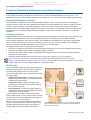
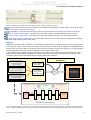
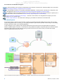
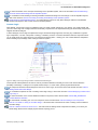
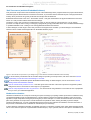
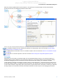
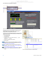
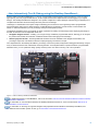
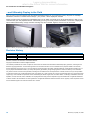
Legacy documentation
refer to the Altium Wiki for current information
An Introduction to Embedded Intelligence
Summary
Guide
GU0123 (v1.0) May 19, 2008
This document provides you with an introduction to the world of Embedded
Intelligence and FPGA design. It takes a look at the design environment provided by
Altium's Innovation Station – including essential design concepts – and also takes a
look at final deployment of a design in the field.
With their ability to operate at high switching frequencies FPGAs have provided an ideal solution for implementing large
amounts of high speed digital logic, allowing the designer to reduce the size and cost of a product.
Today these devices have sufficient capacity to implement more than just some of the hardware in a product – they can be
programmed to implement an entire digital system, including the processor, peripheral components and the interface logic.
To do this the engineer needs a design environment that solves the system integration issues – where they can capture the
hardware design, write the embedded software for the processor, and implement, test and debug both the hardware and
software on the target FPGA.
Altium Designer brings together the required tools and the necessary communications systems. Combine this with the Desktop
NanoBoard reconfigurable hardware platform – the NB2DSK01 – and you have a complete FPGA design environment.
This guide will give you an overview of the key design concepts and the technologies and tools provided by this innovative
design environment – an environment that allows you to quickly and efficiently take your design and turn it from envisioned
dream to deployed reality.
The Altium Innovation Station
Take an FPGA design from concept idea to fruition and you will more than likely have an innovative product on your hands. The
environment needed to capture and develop that design needs to be equally innovative. Altium Designer, combined with the
Desktop NanoBoard, delivers just such an environment.
Referred to as the Altium Innovation Station, this pairing of unified electronics design software with a reconfigurable hardware
platform, provides you with a
design environment that places
embedded intelligence at the
center of the design process.
Altium Designer and the Desktop
NanoBoard work seamlessly
together to provide:
•
One unified software-hardware
design solution
•
One design data model
•
One development platform
•
Complete hardware and
software device vendor
independence
•
Multiple hardware deployment
possibilities.
Figure 1. Altium Designer and the Desktop NanoBoard work in harmony to deliver the ultimate
Innovation Station.
With Altium's Innovation Station the low level detail is managed for you, leaving you free to focus on embedded intelligence and
functionality – the source of true and sustainable product differentiation. The designs you create are limited only by the extent of
your imagination.
GU0123 (v1.0) May 19, 2008
1
Legacy documentation
refer to the Altium Wiki for current information
An Introduction to Embedded Intelligence
Create the Embedded Intelligence using Altium Designer...
Altium Designer brings together hardware, software and programmable hardware design within a single, unified environment.
This integrated environment provides all the tools necessary to create the embedded intelligence for your product – the
hardware design itself and the embedded software which is destined to run on any 'soft' processors defined within that design.
Embedded Intelligence Concepts
From the outside, an FPGA device does not look particularly interesting – 'seen one, seen them all'. Once programmed
however, the device 'comes alive' with engineered functionality, becoming the heartbeat for the electronic product in which it
resides. It is this functionality – or Embedded Intelligence – that we are concerned with when creating an FPGA design.
The actual content of an FPGA design will depend on the nature of that design – the functionality it requires and the end-task
that it is to perform. To effectively develop embedded intelligence, there are some essential concepts that you will need to
understand:
Embedded Intelligence
Embedded Intelligence is an umbrella term for all elements that are downloaded into the product to give it its functionality. This
includes the FPGA design itself, as well as any embedded program code required by processors within that design.
The term reflects perfectly the 'soft' nature of a design, who's intelligence is 'embedded' into a high-capacity programmable
device. By moving functionality out of the physical domain and into the soft, you are able to create the device intelligence
needed to generated sustainable differentiation of your end product in the market place.
The following are just some of the key benefits of 'soft' design:
•
The IP that you program into the system is better protected than physical IP, as the source isn't shipped with the product.
•
Soft design can happen before and after the hardware platform is designed.
•
Soft design can continue after the product is manufactured and deployed to the end customer. This includes aesthetics
implemented in the soft design.
•
Soft design provides the basis for an ecosystem which connects your customer to you, via your products.
How do I choose an FPGA device? – this video looks at how to find the best-suited FPGA to host your design.
Building a complete Embedded FPGA application from scratch – this video takes a look at just how quickly you can create a
complex design, such as a video capture application, using Altium Designer.
FPGA Design
This is the hardware design itself which will be programmed
within the physical device. It will contain all of the logic and
connectivity and typically feature a processor system.
There are three important phases to consider when creating
your FPGA design:
•
Capture & Verification Phase – placing and wiring the
'ingredient' logic for the design and ensuring that it is free
of electrical and drafting errors.
•
Configuration Phase – targeting the design to the
physical device into which it is to be programmed (see
the next section: Mapping).
•
Processing Phase – the job of turning the design from
captured source files into a programming file that can be
downloaded to the targeted device.
In Altium Designer, the design is created and managed
within an FPGA project. In terms of design capture, a variety
of FPGA-ready (and vendor-independent) components are
supplied for use in your FPGA designs.
When it comes to processing the design, Altium Designer
provides a central interface from where the design can be
compiled, synthesized, built (using the appropriate and
installed Vendor tools) and dowloaded into the device.
2
Figure 2. FPGA-ready components – vendor-independent building
blocks that enable designs to be created quickly and retargeted to
alternate physical devices.
GU0123 (v1.0) May 19, 2008
Legacy documentation
refer to the Altium Wiki for current information
An Introduction to Embedded Intelligence
Figure 3. Processing of an FPGA design within Altium Designer – literally at the click of a button!
For an introductory tutorial that covers the basics of FPGA design using the Altium Innovation Station, refer to the document
TU0116 Getting Started with FPGA Design.
For information on processing an FPGA design, refer to the document AP0103 Processing the Captured FPGA Design.
How do I create an FPGA design? – this video covers the basics of getting a simple FPGA design up and running.
How do I build an FPGA design? – this video looks at processing a design and running it on some target hardware.
FPGA Design for Board Level Designers – this video takes a look at how you can leverage your existing board level design
skills to begin designing FPGA circuits today.
Mapping
Mapping is a method by which your design can be interfaced to the physical pins of the FPGA device in which it is programmed.
Put another way, it is the means by which your design can interact with the 'outside world'. By mapping internal digital signals to
the device pins, your logic is able to communicate to other areas of your product. As part of this mapping, you would also define
analog characteristics of the pins, such as IO standards, drive strengths and slew rates.
In Altium Designer, this mapping is achieved using ports (or port components), configurations and constraint files. An FPGA
design can have multiple defined configurations, with each configuration containing the constraint files (pin mappings, clock
constraints, place and route constraints) required to target a different physical device.
FPGA-Ready, Vendor-Independent
Components
FPGA Project
Constraint File Containing
Clock constraints and additional
non-architecture-specific
design constraints
Source Design Files
(Schematic, OpenBus
System, HDL)
Constraint File Containing
Place & Route Constraints for any
Spartan-3 implementation
Daughter Board DB30
Configuration - A
Xilinx Spartan-3
XC3S1500-4FG676C
on
Daughter Board DB30
Constraint Files Containing
Mappings from FPGA Project Ports
to pins of XC3S1500-4FG676C on
Daughter Board DB30
Xilinx Spartan-3
Flow
XC3S1500-4FG676C
Desktop NanoBoard NB2DSK01
Peripheral Board Constraint File
VGA_HSYNC
Video
Output
VGA_VSYNC
Interface
Mapping
Constraint
File
NB2DSK01 Motherboard
Constraint File
Interface
Mapping
Constraint
File
Daughter Board Constraint
File
HDR1
EXT_C
HDR_T
HDR_T
98
98
4
4
A8
100
100
2
2
B8
Xilinx
Spartan-3
FPGA
Example Port-to-Pin Mapping
Figure 4. Targeting a design to a physical device on a daughter board plugged into the Desktop NanoBoard. The example mapping illustrates a
couple of signals associated with a resource on a peripheral board and their subsequent mapping path to the physical pins of the target device.
GU0123 (v1.0) May 19, 2008
3
Legacy documentation
refer to the Altium Wiki for current information
An Introduction to Embedded Intelligence
For more information on the concept of configurations and constraints, and their role in design portability, refer to the article
AR0124 Design Portability, Configurations and Constraints.
For more detailed information on the Desktop NanoBoard NB2DSK01 constraint system, including auto-configuration, refer
to the application note AP0154 Understanding the Desktop NanoBoard NB2DSK01 Constraint System.
For a tutorial that looks at how signal integrity can be used to determine optimum slew and drive settings for specific pins of
an FPGA device, refer to the document TU0126 Checking Signal Integrity on an FPGA Design.
How do I target and constrain an FPGA design? – this video covers creation of a configuration that targets your FPGA
design to run on a specific device.
How do I setup FPGA IO? – this video looks at setting up your FPGA IO to interface to the outside world.
Bus-based System
A 'bus-based system' is the term used to describe a method of connecting functional 'building blocks' of logic into an overall
system, using generic buses. In this way, you can quickly assemble a system that incorporates a diverse range of functionality,
and that will meet the needs of your intended application.
In Altium Designer, such a system is built using the Wishbone bus interconnect and can be implemented as a high-level,
abstract, OpenBus System document, or at the low-level, using Wishbone-compliant components placed on schematic sheets.
OpenBus Systems are the favored approach as they provide an environment in which to build your system that is highly
intuitive, streamlined and less prone to error.
Figure 5. Example bus-based systems in Altium Designer – OpenBus System-based (top) and Schematic-based (bottom).
4
GU0123 (v1.0) May 19, 2008
Legacy documentation
refer to the Altium Wiki for current information
An Introduction to Embedded Intelligence
For more information on the concepts and workings of the OpenBus System, refer to the document AR0144 Streamlining
Processor-based FPGA Design with the OpenBus System.
For a tutorial that looks at taking an existing schematic-based FPGA design and converting it to use the OpenBus System,
refer to the document TU0129 Converting an Existing FPGA Design to the OpenBus System.
FPGA Design for Embedded Developers – this video takes a look at how easy Altium Designer makes it for Embedded
Software Developers to take control over their hardware platform.
Custom Logic
Quite literally, custom logic is logic (or intelligence) that you create yourself and add in to your design. You would typically add
your own custom logic into a design where the functionality required cannot be implemented using the FPGA-ready components
shipped with Altium Designer.
In Altium Designer, custom logic is implemented using a hierarchical design approach, and using any combination of generic
logic components, C or HDL code (VHDL or Verilog). In addition, provision of a Custom Wishbone Interface component allows
you to quickly hook your custom logic into your existing bus-based system – creating your own Custom Wishbone Peripheral –
without needing any knowledge of the workings of that bus system.
Figure 6. Adding custom logic through creation of hierarchical FPGA designs.
Vendor-specific FPGA primitives can also be used to provide the desired functionality, but use of such devices limits the
portability of the design – locking it into a specific device family or, in some cases, specific physical FPGA device.
An example of hierarchical FPGA design and the use of custom logic, can be found in the base tutorial document TU0116
Getting Started with FPGA Design.
For a tutorial that explores the use of creating custom logic using C, refer to the document TU0133 Designing Custom FPGA
Logic using C.
For more information on the Custom Wishbone Interface component, refer to the document CR0187 WB_INTERFACE
Custom Wishbone Interface.
For more details on building your own core component, refer to the document TU0123 Creating a Core Component.
How do I use VHDL or Verilog in an FPGA design? – this video looks at how blocks of VHDL or Verilog can be included in
an FPGA design.
How do I create and share an FPGA Core? – this video looks at creating FPGA components that allow you to reuse your
FPGA design blocks across multiple projects without exposing your IP.
GU0123 (v1.0) May 19, 2008
5
Legacy documentation
refer to the Altium Wiki for current information
An Introduction to Embedded Intelligence
'Soft' Processors (and their Embedded Software)
'Soft' processors are processors that are defined as part of the FPGA design that is programmed into the physical FPGA device,
rather than physical, discrete devices connected to the FPGA, or processors that are immersed as part of the physical FPGA's
makeup. Such processors are typically 32-bit and have simple, RISC architectures.
Embedded software refers to the code – the software 'smarts' – that gets downloaded to the physical FPGA device and which
will run on a soft processor defined within the FPGA design.
The beauty of using 'soft' processors in FPGA designs is that you are not locked to a physical device. You can change
processor or modify the code running on it simply by reprogramming the physical FPGA device with a modified hardware design
or updated embedded code – leading to true 'field upgradeable hardware and software'.
In Altium Designer, a wide range of 32-bit 'soft' processors are supported for use within your FPGA designs. The associated
software code is created and managed within an Embedded Software project.
Figure 7. Add a 32-bit 'soft' processor to your design and go to town with the associated embedded code functionality.
For an introductory tutorial that looks at an FPGA design incorporating a 32-bit processor, refer to the document TU0128
Implementing a 32-bit Processor-based Design in an FPGA.
For an introductory tutorial that explores Embedded Software design in Altium Designer, refer to the document TU0122
Getting Started with Embedded Software.
How do I decide which processor to use? – this video gives a brief overview of the various processors supported by Altium
Designer and how to choose the one that is right for your application.
How do I add peripherals and IO to my processor? – this video looks at using Wishbone to customize the mix of peripherals
that you use in your embedded application.
Hardware Acceleration
Hardware acceleration is the concept of enhancing the speed of a design by imparting software processes into hardware. Many
computational algorithms that are straightforward to code and debug in software are inherently parallel in nature. Encryption
algorithms, image manipulation and signal processing are just some examples. To remain as software entities, such functions
place heavy demands on the processor. FPGAs themselves are parallel in nature, offering the ability to perform multiple
operations simultaneously. To move computationally-intensive functions from software into hardware, and ease the burden of
the processor, would therefore be considered an evolutional jump for the design.
In Altium Designer, hardware acceleration is facilitated using the C-to-Hardware Compiler (CHC), which takes standard untimed
ISO-C source code and produces a synthesizable hardware file (RTL). Upon synthesis, this RTL description is translated into an
6
GU0123 (v1.0) May 19, 2008
Legacy documentation
refer to the Altium Wiki for current information
An Introduction to Embedded Intelligence
electronic circuit that implements the function required. A 'soft' processor in the FPGA design accesses these hardware
functions through use of an Application-Specific Processor (ASP).
Figure 8. The ASP component interfaces between the code running on the processor and the functions implemented in the FPGA fabric.
For a tutorial that explores the use of hardware acceleration in an FPGA design, refer to the document TU0130 Getting
Started with the C-to-Hardware Compiler.
For detailed reference information on the C-to-Hardware Compiler, refer to the document GU0122 C-to-Hardware Compiler
User Manual.
For information on the ASP component, refer to the document CR0177 WB_ASP Configurable Application Specific
Processor.
Debugging
Debugging is the act of testing you hardware design and any embedded software (running on 'soft' processors therein), to
obtain the desired (correct) performance and functionality. Debugging is an important element of the overall design strategy,
and effective debugging can save a lot of time and money when it comes time to deploy your end design in the field.
In Altium Designer, debugging of hardware is provided courtesy of 'virtual' instruments – components which are 'wired' into the
actual FPGA design but which, on programming the physical device, offer software-based controls for interrogation and control
of nodes within the design. Imagine being able to jump inside the physical FPGA device, armed with an oscilloscope, multimeter
and logic analyzer, and you'll have some idea of what these instruments can offer as part of a 'live' debugging environment.
GU0123 (v1.0) May 19, 2008
7
Legacy documentation
refer to the Altium Wiki for current information
An Introduction to Embedded Intelligence
Figure 9. Monitor and control I/O using a custom instrument – just one of a variety of virtual instruments for use in an FPGA design.
Embedded software can be debugged in real-time, once the
FPGA design and associated program code have been
programmed into the physical FPGA device.
The debug environment offers the full suite of tools you would
expect to see in order to efficiently debug the embedded code.
These features include:
•
Setting Breakpoints
•
Adding Watches
•
Stepping into and over at both the source (*.C) and
instruction (*.asm) level
•
Reset, Run and Halt code execution
•
Run to cursor.
An example of using virtual instrumentation in an FPGA
design can be found in the base tutorial document TU0116
Getting Started with FPGA Design.
For a tutorial that looks at using the Custom Instrument
component, refer to the document TU0135 Adding Custom
Instrumentation to an FPGA Design.
How do I use instruments in my FPGA design? – this video
looks at the use of embedded instruments in an FPGA
design.
Figure 10. Entering an embedded code debug session.
8
GU0123 (v1.0) May 19, 2008
Legacy documentation
refer to the Altium Wiki for current information
An Introduction to Embedded Intelligence
...then Interactively Test & Debug using the Desktop NanoBoard...
Altium's Desktop NanoBoard NB2DSK01 is a unique, reconfigurable hardware platform that harnesses the power of today's
high-capacity, low-cost programmable devices, to allow rapid and interactive implementation and debugging of your digital
designs. The Desktop NanoBoard is designed to be a perfect complement to Altium Designer, transforming your desktop into a
complete and interactive electronics design laboratory that uses LiveDesign.
LiveDesign is a unified electronics system design methodology that is based on 'live' engineering inside a programmable
physical hardware design space. Altium Designer, the NanoBoard and LiveDesign, provide real-time communication and
'hands-on' interaction between you and your design during the development process.
The Desktop NanoBoard gives you the ability to design, implement and debug an entire design before deploying that design in
the field. At the heart of its reconfigurable nature are:
•
Swappable daughter boards – enabling you to target a range of different programmable devices, allowing you to compare
the performance benefits and trade-offs of different FPGAs without changing the actual design.
•
Satellite peripheral boards – delivering additional hardware resources available to the daughter board FPGA, and
providing a simple and cost-effective method for rapid prototyping of hardware concepts.
Once implemented on the Desktop NanoBoard, your design can then be probed, analyzed and debugged interactively using an
array of virtual instruments and JTAG-based monitoring features. As the implementation is performed within a programmable
hardware realm, you can update the design quickly and many times over without incurring cost or time penalties.
Figure 11. Altium's Desktop NanoBoard NB2DSK01.
For detailed information on the NB2DSK01, refer to the document TR0143 Technical Reference Manual for Altium's Desktop
NanoBoard NB2DSK01.
For information on communications between the Desktop NanoBoard and the PC, refer to the document AR0130 PC to
NanoBoard Communications.
For information on the range of supported daughter and peripheral boards available for the Desktop NanoBoard, and
additional documentation specific to each, go to www.altium.com/nanoboard/resources.
GU0123 (v1.0) May 19, 2008
9
Legacy documentation
refer to the Altium Wiki for current information
An Introduction to Embedded Intelligence
...and Ultimately Deploy to the Field
Once you have your FPGA design (and associated embedded software for any processors) running 'bug-free' on a Desktop
NanoBoard, it is time to consider how that design – your product – will be deployed in the field.
Altium provides a range of Deployment NanoBoards that you can either use entirely as an off-the-shelf solution or that you can
customize with your own peripheral boards. Alternatively you can go for a fully custom PCB solution. The choice of deployment
options will be influenced by a range of factors including cost, time to market, logistics, and form and fit constraints.
Figure 12. Move your product to the field using one of the available Deployment NanoBoard solutions.
Revision History
Date
Version No.
Revision
19-May-2008
1.0
Initial release
Software, hardware, documentation and related materials:
Copyright © 2008 Altium Limited. All Rights Reserved.
The material provided with this notice is subject to various forms of national and international intellectual property protection, including but not
limited to copyright protection. You have been granted a non-exclusive license to use such material for the purposes stated in the end-user
license agreement governing its use. In no event shall you reverse engineer, decompile, duplicate, distribute, create derivative works from or in
any way exploit the material licensed to you except as expressly permitted by the governing agreement. Failure to abide by such restrictions
may result in severe civil and criminal penalties, including but not limited to fines and imprisonment. Provided, however, that you are permitted
to make one archival copy of said materials for back up purposes only, which archival copy may be accessed and used only in the event that the
original copy of the materials is inoperable. Altium, Altium Designer, Board Insight, DXP, Innovation Station, LiveDesign, NanoBoard, NanoTalk,
OpenBus, P-CAD, SimCode, Situs, TASKING, and Topological Autorouting and their respective logos are trademarks or registered trademarks
of Altium Limited or its subsidiaries. All other registered or unregistered trademarks referenced herein are the property of their respective owners
and no trademark rights to the same are claimed. v8.0 31/3/08.
10
GU0123 (v1.0) May 19, 2008