1
Getting Started with the
C−to−Hardware Compiler
TU0130 May 16, 2008
Software, hardware, documentation and related materials:
Copyright E 2008 Altium Limited. All Rights Reserved.
The material provided with this notice is subject to various forms of national and international intellectual property protection, including but not
limited to copyright protection. You have been granted a non−exclusive license to use such material for the purposes stated in the end−user
license agreement governing its use. In no event shall you reverse engineer, decompile, duplicate, distribute, create derivative works from or in
any way exploit the material licensed to you except as expressly permitted by the governing agreement. Failure to abide by such restrictions may
result in severe civil and criminal penalties, including but not limited to fines and imprisonment. Provided, however, that you are permitted to
make one archival copy of said materials for back up purposes only, which archival copy may be accessed and used only in the event that the
original copy of the materials is inoperable. Altium, Altium Designer, Board Insight, DXP, Innovation Station, LiveDesign, NanoBoard, NanoTalk,
OpenBus, P−CAD, SimCode, Situs, TASKING, and Topological Autorouting and their respective logos are trademarks or registered trademarks
of Altium Limited or its subsidiaries. All other registered or unregistered trademarks referenced herein are the property of their respective owners
and no trademark rights to the same are claimed.
ii
Table of Contents
Table of Contents
Introduction to the C−to−Hardware Compiler
1.1
1.2
1.3
Using the CHC Compiler . . . . . . . . . . . . . . . . . . . . . . . . . . . . . . . . . . . . . . . . . . . . . . . . . . . . . . . . . . .
Required Knowledge to use the CHC Compiler . . . . . . . . . . . . . . . . . . . . . . . . . . . . . . . . . . . . . . .
Suggested Reading . . . . . . . . . . . . . . . . . . . . . . . . . . . . . . . . . . . . . . . . . . . . . . . . . . . . . . . . . . . . . . .
Elaborated Project with Hardware Acceleration
2.1
2.2
2.2.1
2.2.2
2.2.3
2.2.4
2.3
2.3.1
2.3.2
Introduction . . . . . . . . . . . . . . . . . . . . . . . . . . . . . . . . . . . . . . . . . . . . . . . . . . . . . . . . . . . . . . . . . . . . . .
Modify the Project . . . . . . . . . . . . . . . . . . . . . . . . . . . . . . . . . . . . . . . . . . . . . . . . . . . . . . . . . . . . . . . .
Modify the FPGA−project . . . . . . . . . . . . . . . . . . . . . . . . . . . . . . . . . . . . . . . . . . . . . . . . . . . . . . . . . .
Configure Memory and Recompile Project . . . . . . . . . . . . . . . . . . . . . . . . . . . . . . . . . . . . . . . . . . .
Modify the Software . . . . . . . . . . . . . . . . . . . . . . . . . . . . . . . . . . . . . . . . . . . . . . . . . . . . . . . . . . . . . . .
Build the Project . . . . . . . . . . . . . . . . . . . . . . . . . . . . . . . . . . . . . . . . . . . . . . . . . . . . . . . . . . . . . . . . . .
Accelerate by Compiling C−to−Hardware . . . . . . . . . . . . . . . . . . . . . . . . . . . . . . . . . . . . . . . . . . . .
Add ASP and Connect it to TSK3000A and Memory . . . . . . . . . . . . . . . . . . . . . . . . . . . . . . . . . . .
Build the Project . . . . . . . . . . . . . . . . . . . . . . . . . . . . . . . . . . . . . . . . . . . . . . . . . . . . . . . . . . . . . . . . . .
1−1
1−2
1−3
1−3
2−1
2−1
2−2
2−2
2−5
2−8
2−9
2−10
2−10
2−16
iii
Getting Started with the C−to−Hardware Compiler
iv
1 Introduction to the C−to−Hardware Compiler
Summary
This chapter explains the essence of the C−to−Hardware Compiler. It tells how you
can use this compiler to design hardware ’functions’ using ordinary C language,
resulting in a dramatic performance increase of your embedded application.
What is the C−to−Hardware Compiler?
The C−to−Hardware Compiler (CHC) compiler resembles a normal toolset (compiler, assembler, linker, locator) but instead of
producing a software file, it produces a hardware file that can be loaded onto an FPGA.
The C−to−Hardware Compiler accepts standard untimed ISO−C source code as input and produces a synthesizable hardware
file. The synthesis tools of Altium Designer translate this hardware file into an electronic circuit which can be loaded onto an
FPGA along with the rest of the design and the software.
How is the C−to−Hardware Compiler used?
In Altium Designer, the C−to−Hardware Compiler can be used in two ways:
1. To compile an embedded program to software and selected functions to hardware. The hardware functions can still be called
from the software. This means you can write an ’ordinary’ C program for a processor core. Using Altium Designer, you can
mark which functions should be compiled to hardware. Your FPGA design then needs an Application Specific Processor
(ASP) to hold these compiled hardware functions.
2. To create a piece of FPGA logic by compiling it’s associated C source to hardware. The generated logic acts as a
component on the FPGA sheet. In contrast to above, it is not part of an embedded software program.
In this tutorial, the first situation is demonstrated: we will compile an embedded program and tell the C−to−Hardware compiler to
compile one time consuming function to hardware. For that, we will create an FPGA sheet that contains an ASP.
When compiling and synthesizing your project (embedded software and hardware), either the regular C compiler or the
C−to−Hardware compiler is invoked depending on whether you marked functions as hardware or not.
The final result, after having compiled the application and having loaded both software and hardware onto an FPGA, is a system
where the software and the synthesized hardware functions form the implementation of your original C program. The software
part ’calls’ hardware functions that perform their task far more efficiently than if they were compiled to software.
What are the benefits of the C−to−Hardware Compiler?
Virtually all C programs (or functions) can be converted to an electronic circuit by the C−to−Hardware Compiler. However, the
characteristics of the program determine whether the C−to−Hardware Compiler can create an efficient hardware component or
whether it is better to execute the program on a processor core. The C−to−Hardware Compiler can only create a small and fast
electronic circuit if the C source code is parallelizable. In such a case the hardware executes many operations in parallel
whereas a processor core would fetch and execute instructions sequentially.
Graphics, signal processing and encryption algorithms translate very well into hardware and performance improves by orders of
magnitude. For these types of algorithms FPGA implementations outperform high−end DSP and RISC processor cores.
So the main benefit of the C−to−Hardware Compiler is, that it lets you design hardware modules to perform specific tasks by
simply programming them in C. Normally this would be a complex and time−consuming job that would have to be performed by
specialized hardware designers.
1−1
Getting Started with the C−to−Hardware Compiler
1.1
Using the CHC Compiler
For a regular embedded project, the CHC compiler will not be invoked. In this situation only the FPGA design is synthesized and
loaded onto an FPGA together with a ready compiled embedded project.
The C−to−Hardware Compiler is actually a complete toolset, including a compiler, assembler and linker, conceptually
very similar to a regular C toolset.
The CHC compiler is invoked when the FPGA design gives cause to do so:
• the FPGA design contains one or more Application Specific Processor (ASPs) components, which are able to hold the
hardware equivalent of a C software function,
• the configuration of the ASP−component describes that it contains at least one hardware compiled C function.
When building the project, based on the configuration settings of the ASPs on the schematic, a list of function qualifiers is
generated that mark the functions to be compiled to hardware. This function qualifier file is submitted both to the regular
embedded toolset and to the CHC toolset. The embedded toolset now "knows" which functions should be compiled to hardware.
It does not compile these functions, but generates a wrapper with just enough code to call the hardware function, to pass any
variables, and to receive the return value. The result is an absolute ELF object file.
The same C sources and function qualifier file are submitted to the CHC toolset. Based on the function qualifier file, the CHC
toolset compiles and assembles the marked C functions to hardware. The result, is an absolute ELF object file which contains
the hardware functions.
The ELF file with the hardware functions will be translated into VHDL or Verilog by the HDL generator. Then it is synthesized,
along with the rest of the FPGA design, resulting in a BIT file which can be loaded onto the FPGA. The ELF file with the software
functions is already in its final state and will be loaded into the processor soft−core on the FPGA.
Debugging
You can debug the resulting .elf file of the embedded software as with any embedded software project. However, the
embedded project does not contain the hardware functions, only a wrapper to call those functions. Therefore you cannot step
into the hardware function, but you can set a breakpoint just before and after a hardware function to inspect the entry and exit
conditions.
To avoid this restriction, it is recommended to debug the source code entirely as software first. As mentioned before, your FPGA
design needs to have an Application Specific Processor component. The configuration of this component determines which
functions should be compiled to hardware. With one extra option, you can force all functions to be compiled to regular software:
3. On the schematic, right−click on the WB_ASP component and select Configure id (WB_ASP)...
The configure (WB_ASP Properties) dialog opens.
4. Disable the option Use ASP from Software.
When building the project, all C functions are now compiled (and called) as regular software functions, regardless of whether
they were marked as hardware or not. This enables you to normally debug the software project before turning some functions
into hardware.
1−2
Introduction to the C−to−Hardware Compiler
1.2
Required Knowledge to use the CHC Compiler
Familiarity with the C programming language is essential. Experience with optimizing your code for a given target processor
architecture helps to decide which code fragments would probably benefit most from compilation to hardware. Knowledge about
hardware design languages is not required.
After compilation, the generated HDL file must be integrated with the rest of the hardware design. Subsequently the resulting
design must be instantiated on the FPGA. In Altium Designer this process is fully automated.
1.3
Suggested Reading
The following documents provide a helpful introduction into FPGA and Embedded Software design in Altium Designer:
−
TU0116 Getting Started with FPGA Design
−
TU0122 Getting Started with Embedded Software
−
TU0128 Implementing a 32−bit Processor−based Design in an FPGA
For more detailed information on the C−to−Hardware Compiler, refer to the document:
−
GU0122 C−to−Hardware Compiler User Manual
For more detailed information on the configurable Application Specific Processor (ASP) peripheral device:
−
CR0177 WB_ASP Configurable Application Specific Processor
You can find these documents in the ...\Help directory of Altium Designer’s installation directory. You can either access them
from there directly, or locate and launch them from the lower region of the Knowledge Center panel (From the Help menu, select
Knowledge Center).
1−3
2 Elaborated Project with Hardware
Acceleration
Summary
2.1
This tutorial shows how the C−to−Hardware Compiler is used to obtain performance
increase. It takes the FPGA design of tutorial Implementing a 32−bit
Processor−based Design in an FPGA (TU0128) as a starting point. To this design an
Application Specific Processor (ASP) component is added which will hold a hardware
function that will be compiled from software. You will clearly observe the performance
gain.
Introduction
This tutorial is continues from the result of the tutorial TU0128 Implementing a 32−bit Processor−based Design in an FPGA. A
piece of hardware including a processor soft−core and a row of LEDs was created as well as the software that caused the LEDs
to count in a binary way.
You may either walk through that tutorial first and then continue with this tutorial, or, if you wish to skip it, you can simply open
the resulting project from that tutorial.
If you have not done so:
• Start Altium Designer
1. From the File menu, select Open...
The Choose Document to Open dialog opens in the Examples directory.
2. Browse to the directory Tutorials » FPGA Processor Design 32 bit.
3. Open the project file FPGA_Processor_32Bit.PrjFpg.
To prevent the original tutorial project from being modified, you may want to keep a copy of it!
You are now ready to start with the tutorial.
Outline of the tutorial
In the previous tutorial, we created a 32−bit Processor−based FPGA design and programmed it with a piece of software. We did
not use the C−to−hardware Compiler yet, because in our simple design there was nothing to gain.
In this tutorial, we will first add some external memory and replace the delay loop in the software by a CRC calculation on the
contents of this (otherwise not used) memory. Compared to the example in the previous tutorial, this will slow down the speed at
which the LEDs are counting.
After that, we will modify the example in such a way, that parts of the software can be translated to hardware which should
clearly result in a performance increase. We will therefore add an application specific processor (ASP) to the design which can
be programmed with a C function that will be compiled to hardware.
2−1
Getting Started with the C−to−Hardware Compiler
2.2
Modify the Project
First, we will modify the schematic by adding extra memory. We will configure this memory and recompile the project. Then we
will modify the C source so it performs a time−consuming CRC calculation on the memory, causing a delay in the speed at
which the LEDs are counting.
Finally we will rebuild the project and load it onto the FPGA on the NanoBoard. Let’s start.
2.2.1
Modify the FPGA−project
1. Add a Wishbone interconnect to the memory bus of the TSK3000A
1. Make sure the schematic BlinkingLED.SchDoc is open.
2. Remove the No−ERC markers, the VCC connection and the GND connection from the right side of the TSK3000A
component.
3. If not done so, open the Libraries panel: click on the System button at the right bottom fo your screen and make sure
Libraries is checked.
4. On the Libraries panel: from the FPGA Peripherals.IntLib library, drag the WB_INTERCON component to your sheet and
connect it to the TSK3000A component.
5. Right−click on the Wishbone interconnect component and select Configure U?(WB_INTERCON)...
The Configure (Wishbone Intercon) dialog appears.
A. Globally configure the component. At the right bottom of the dialog:
• Set Unused Interrupts to No Interrupt output pin.
• Set Master Address Size to 32−Bit (Memory).
B. Add a ROM memory to the configuration:
• Click the Add Device... button.
The Device Properties dialog appears.
Change the following settings:
•
•
•
•
•
•
2−2
Give the device an Identifier (for example xrom) and set Type to ROM.
Set the Address Bus Mode to Byte Addressing.
Set the Address Base to 0100 0000.
Set Decode Addressing to 8.
Set the Address Bus Width to 20 Bits − Range = 1 MB.
Set the Data Bus Width to 32−bit.
Elaborated Project with Hardware Acceleration
6. Click OK to confirm all settings and close the dialogs.
2. Add a memory controller to the interconnect
1. On the Libraries panel: from the FPGA Peripherals.IntLib library, drag the WB_MEM_CTRL component to your sheet and
connect it to the Wishbone interconnect we just placed.
2. Right−click on the memory controller component and select Configure U?(WB_MEM_CTRL)...
The Configure (Memory Controller) dialog appears.
We are going to use the static RAM that is available on the daughterboard.
This is asynchronous SRAM, 1 MB (256K x 32−bit) in 2 x 16−bit Wide Device layout:
• Enter these settings in the dialog and click OK to confirm the new settings.
2−3
Getting Started with the C−to−Hardware Compiler
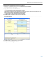
3. Add memory
Now we are going to add the memory itself:
1. On the Libraries panel: from the FPGA DB Common Port−Plugin.IntLib library, drag the SRAM_DAUGHTER0 and
SRAM_DAUGHTER1 components to your sheet and connect them to the SRAM controller we just placed.
Your schematic should now look like this:
Designate the new components:
2. From the Tools menu, select Annotate Schematics Quietly...
A popup box informs you there are two designators that require update and asks if you want to proceed.
• Click Yes to proceed.
All components will now have unique identifiers.
2−4
Elaborated Project with Hardware Acceleration
2.2.2
Configure Memory and Recompile Project
Next, we need to configure the memory for the TSK3000A. In other words, we need to tell the TSK3000A which memory is
available and at which addresses. But be watchful, we also want to retain the mappings that were already defined for the
processor.
1. Configure memory for the TSK3000A
1. Right click on the TSK3000A component and choose Configure Processor Memory.
The Configure Processor Memory dialog appears, showing a graphical representation of the memory for the TSK3000A.
2. Simply click on the Import From Schematic button.
• You are asked whether to delete existing memories. Click No.
A dialog appears that shows the names of the memories.
3. Click on the Do not import cell associated with the interconnect’s name (U5) and
change it to Import.
All sub−entries are changed to import as well.
4. Click OK to confirm the new settings and to return to the main dialog.
The xrom memory is now visible in the Device Memory view.
The final result should look like:
5. Click OK to confirm all settings and to close the main dialog.
2−5
Getting Started with the C−to−Hardware Compiler
2. Save and recompile the project
Save your project using Save All:
1. On the Projects panel: click the Workspace button and select Save All.
Now recompile the project:
2. Right−click on the name of the project and select Recompile FPGA project project_name.PrjFpg.
Two additional definitions have been made in the hardware.h C header file defining a) the base address and b) the size of
the external memory we just added and configured.
3. To save the updated FPGA project, click the Workspace button and select Save All.
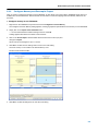
3. Configure Application Memory in the embedded project
We have equipped the TSK3000A processor core on the schematic with1MB of additional external ROM. Now we need to
configure the embedded project as well, so the compiler ’knows’ how the software can access this memory. We need to be map
the Application Memory onto the device memory of the TSK3000A. First go back to your embedded project.
1. Right−click on the embedded project .PrjEmb and select Project Options...
The Options for Embedded Project .PrjEmb dialog appears.
2. Open the Configure Memory tab.
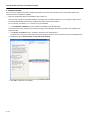
The TSK’s Device Memory already has been imported, but the Application Memory column shows a blue block indicating
available space for mapping.
3. Right−click in the list with memories, and select Delete All (on layer).
In the right Application Memory column, the memories have disappeared while their spaces became blue.
4. Right−click in the Application Memory column (or in the memory list below) and select Add Memory...
The Processor Memory Definition Dialog appears.
•
•
•
•
•
Change the memory’s Name to something more meaningful: xrom.
Verify that the memory’s Type is set to ROM.
Change the memory’s Size to 1M (as we have 2 x 512 MB of external memory on the FPGA sheet).
Change the memory’s Address Base to 0x1000000.
Click OK to confirm the new settings.
You return to the main Options for Embedded Project .PrjEmb dialog.
The Device Memory now shows correctly the additional xrom we defined for the TSK3000A. The Application memory now
shows how it can be accessed from the software. The green color indicates that there are no memory conflicts. The dialog
should now look like this:
2−6
Elaborated Project with Hardware Acceleration
5. Click OK to confirm all settings and to close the main dialog.
Save your project with Save All.
2−7
Getting Started with the C−to−Hardware Compiler
2.2.3
Modify the Software
The hardware project has been modified, so now we will make changes to the software. We will replace the empty loop by a call
to a function that calculates the CRC of the 1 MB memory.
1. Open the C source file (leds1.c) and modify the code as follows:
#include <stdlib.h>
#include <stdint.h>
#include "hardware.h"
volatile uint8_t * const leds = (void *)Base_GPIO;
uint16_t crc16 ( uint8_t * ptr, size_t count);
void main( void )
{
*leds = 0; // Initialize the LEDs to all OFF
for ( ;; )
{
(*leds)++;
crc16( (uint8_t *)Base_xrom, Size_xrom );
}
}
uint16_t crc16( uint8_t * ptr, size_t count)
{
uint16_t crc = 0;
do
{
crc = crc ^(uint16_t)*ptr++ << 8;
for ( int bitcount = 0; bitcount < 8; bitcount++ )
{
if (crc & 0x8000)
crc = crc << 1 ^0x1021;
else
crc <<= 1;
}
} while(−−count );
return crc;
}
2. To save the updated embedded project, click the Workspace button and select Save All.
2−8
Elaborated Project with Hardware Acceleration
2.2.4
Build the Project
Now, the whole project has been modified and it is ready to be built. Make sure the NanoBoard is switched on and properly
connected to your PC.
1. From the View menu, select Devices View.
Below the Spartan3 symbol, there is a wide drop down list.
2. If not selected, select the FPGA_Processor_32Bit / NB2DSK01_07_DB30_04 project / configuration.
3. Make sure the options Ignore FPGA source and Ignore software are disabled as both need to be rebuild.
4. Click on the Program FPGA button on the right side of the Devices view.
The project is built in several stages. This may take a while.
After the project has been built succesfully, it is loaded into the FPGA on the NanoBoard and the LEDs start counting in a binary
way but much more slowly than with the original design. Obviously, calculating a 16−bit CRC from a 1 MB memory block takes a
while.
In the next section we will make further changes to this project. To prevent the project thusfar from being modified, you may
want to keep a copy of it.
2−9
Getting Started with the C−to−Hardware Compiler
2.3
Accelerate by Compiling C−to−Hardware
Now, we expect this CRC16 function to run much faster when compiled in hardware. The C−to−Hardware Compiler (CHC)
generates the hardware, but we need to control the generated hardware from our software. Therefore, the hardware must be
wrapped into an Application Specific Processor (ASP).
When the TSK3000A starts a hardware compiled function, it will transfer the function’s parameters to the ASP, starts the
hardware function and waits until it has finished. Thus, we have to add the ASP to the schematic first.
2.3.1
Add ASP and Connect it to TSK3000A and Memory
The ASP as we will add it to the schematic, contains nothing more than the physical connections neccessary to interact with the
TSK3000A processor core and the external memory. The ASP gets functional when it is programmed with the to hardware
compiled C source.
1. Add the ASP component and connect it to the Wishbone interconnect
1. On the Libraries panel: from the FPGA Peripherals.IntLib library, drag the WB_ASP component to your sheet.
• Place it right below the WB_PRTIO component.
As you can see, the peripheral has two Wishbone buses. The Wishbone bus with the labels that start with io_ is the control
bus that should be connected to the TSK3000A. Thus, you need to modify the Wishbone interconnect component so that this
new peripheral is known. (The second bus with the labels that start with me_ is the memory bus.)
2. Right−click on the Wishbone Interconnect component (U2) and select Configure U2 (WB_INTERCON)...
The Configure (Wishbone Intercon) dialog appears:
A. The ASP is a full 32−bit peripheral that uses word addressing. Add the ASP port to the configuration:
• Click the Add Device... button.
The Device Properties dialog appears.
Change the following settings like listed below and shown in the figure:
•
•
•
•
2−10
Give the port an Identifier (for example ASP) and set Type to ASP.
Set the Address Bus Mode to Word Addressing.
Set the Base Address to 100000.
Set the Address Bus Width to 4 Bits − Range = 16.
Elaborated Project with Hardware Acceleration
• Click OK to confirm the new settings.
A summary of the properties you’ve just set is shown in the Configure dialog.
• Click OK to close the dialog and to return to the schematic.
You may notice that graphically there is not enough space to move the ASP into position so that it nicely connects to the
interconnect component. You can change this as follows:
• Go back to the interconnect configuration dialog and double−click the GPIO component to access its settings.
• Set the Graphical Attribute to, for example, 8 spaces instead of 4 as it does per default.
This shifts the pins for the ASP interface down by 4 spaces.
3. Connect the ASP to the Wishbone interconnect.
2−11
Getting Started with the C−to−Hardware Compiler
2. Add Wishbone Master to the schematic
The second bus on the ASP with the labels that start with me is the memory bus. This bus is used by the generated hardware to
access the external memory. Our memory however provides a single master bus only, so we need an "arbiter" that controls
which part has access to the memory.
1. On the Libraries panel: from the FPGA Peripherals.IntLib library, drag the WB_MULTIMASTER component to your sheet.
This master must be connected between the TSK3000A and the Wishbone Interconnect (U5) that controls the memory:
• Select all neccesary components and move them to the left or right to make space for the multimaster controller.
• Move the multimaster in its place between the TSK3000A and the interconnect.
• Make sure it connects to both the TSK3000A and the interconnect.
2. Open the configuration dialog of the multimaster component.
There are two modes in which the multimaster can do its arbitration: round robin or priority based.
Round robin: when two peripherals want to access the memory bus at the same time and the multimaster is in round robin
mode, it switches between the two masters continuously.
Priority mode: if the multimaster is in priority mode, the master with the highest priority gets access to the bus first.
Although in this example the ASP will never compete with the processor for the same memory, we will put the multimaster in
priority mode and give m2 (the ASP) priority over m1 (the TSK3000A).
• Set Type to Priority.
• Set the Priority of m1 to 2 and set the Priority of m2 to 1.
However, the TSK3000A will be the Master With No Delay (if the bus is idle, by default it switches to this master. If the other
master wants access, it takes an extra cycle to gain access).
• Verify that the Master With No Delay is set to m1 (default)
• Click Ok to confirm the new settings.
3. Connect the Wishbone master to the ASP:
Like for the ASP, graphically we need some extra space to align the m2_ pins of the Multi Master component with the me_
pins of the ASP component. This will allow us to align the multimaster’s m2 interface with the ASP’s memory interface.
• In the configuration dialog, set Spaces After Pins for m1 to, let us say, 29.
Check your schematic and if necessary, change this value to obtain proper alignment.
• Connect the ASP’s secondary port to the multimaster’s secondary port.
2−12
Elaborated Project with Hardware Acceleration
4. Annotate the new components as usual:
• From the Tools menu select Annotate Schematics Quietly...
The modified part of your schematic should then look like this:
2−13
Getting Started with the C−to−Hardware Compiler
3. Configure the ASP
We have not yet configured the ASP. Configuring the ASP is is the base of this tuturial: here we decide which parts of the
software should be compiled to hardware.
1. Open the configuration dialog of the Wishbone ASP component.
There are lists of functions and global variables on the right side of the dialog. With these, you can specify what functions
and what global variables should go into hardware and which should stay in software.
For our example, we want the crc16 function to go into hardware:
• In the Implement in Hardware column, enable the checkbox for the crc16 function.
Since the function will be called from the software running on the TSK3000A, we want the hardware to be available from
outside the ASP:
• In the Export to Software column, enable the checkbox for the crc16 function.
(If we had any functions that where called from other hardware functions, these would not need to be marked Exported).
• Enable both options Generate ASP and Use ASP from Software.
• Click OK to confirm the new settings.
2−14
Elaborated Project with Hardware Acceleration
4. Configure the TSK3000A to add the ASP as a peripheral
1. Right click on the TSK3000A component and select Configure Processor Peripheral...
The Configure Peripherals dialog appears.
2. Simply click on the Import From Schematic button.
• You are asked whether to delete existing peripherals. Click No.
A dialog appears that shows the names of all peripherals, sorted by the Wishbone interconnect they are defined in. The
dialog lists the U2 component with the GPIO block and the ASP block.
• Import the ASP only. (The GPIO block has already been added).
3. Click OK to confirm the new settings and to return to the main dialog.
The ASP peripheral is now visible in the Defined Peripheral Devices view. Note that the denoter U2 refers to the Wishbone
interconnect component.
4. Click OK to confirm all settings and to close the main dialog.
5. Save your project with Workspace » Save All.
2−15
Getting Started with the C−to−Hardware Compiler
2.3.2
Build the Project
Now, the whole project has been finished and it is ready to be built. Make sure the NanoBoard is switched on and properly
connected to your PC.
1. From the View menu, select Devices View.
Below the Spartan3 symbol, there is a wide drop down list.
2. If not selected, select the FPGA_Processor_32Bit / NB2DSK01_07_DB30_04 project / configuration.
3. Make sure the options Ignore FPGA source and Ignore software are disabled as both need to be rebuild.
4. Click on the Program FPGA button on the right side of the Devices view.
The project is built in several stages. This may take quite some time, especially the build stage may take a while.
After the project has been built succesfully, it is loaded into the FPGA on the nanoboard and the LEDs start counting in a binary
way, but much faster than they did before thanks to the hardware execution of the crc16 function.
Revision History
Date
Version No.
Revision
12−Nov−2007
1.0
Initial Release
16−May−2008
1.1
Updated to reflect new C−to−Hardware compiler features. Converted to A4.
Software, hardware, documentation and related materials:
Copyright E 2008 Altium Limited. All Rights Reserved.
The material provided with this notice is subject to various forms of national and international intellectual property protection, including but not
limited to copyright protection. You have been granted a non−exclusive license to use such material for the purposes stated in the end−user
license agreement governing its use. In no event shall you reverse engineer, decompile, duplicate, distribute, create derivative works from or in
any way exploit the material licensed to you except as expressly permitted by the governing agreement. Failure to abide by such restrictions may
result in severe civil and criminal penalties, including but not limited to fines and imprisonment. Provided, however, that you are permitted to
make one archival copy of said materials for back up purposes only, which archival copy may be accessed and used only in the event that the
original copy of the materials is inoperable. Altium, Altium Designer, Board Insight, DXP, Innovation Station, LiveDesign, NanoBoard, NanoTalk,
OpenBus, P−CAD, SimCode, Situs, TASKING, and Topological Autorouting and their respective logos are trademarks or registered trademarks
of Altium Limited or its subsidiaries. All other registered or unregistered trademarks referenced herein are the property of their respective owners
and no trademark rights to the same are claimed.
2−16