1
MC68838UM/AD
FDDI '
-'- '.,... -
Fiber Distributed Data Interface
User's Manual
MC68838
®
MOTOROLA
Introduction
Functional Description
II
IJ
Signal Description
II
II
Bus Operation
II
Register Description
Receive Data Path Operation
II
II
Transmit Data Path Operation
III
MAC-PHY Interface Operation
Test Operation
III
1m
Electrical Characteristics
III
Ordering Information and Mechanical Data
IE
CAM Interface Operation
II
II
II
II
Ell
_
II
II
III
mil
III
lEI
Introduction
Functional Description
Register Description
Signal Description
Bus Operation
MAC-PHV Interface Operation
Receive Data Path Operation
Transmit Data Path Operation
CAM Interface Operation
Test Operation
Electrical Characteristics
Ordering Information and Mechanical Data
®
MOTOROLA
MC68838
Media Access Controller
User's Manual
Motorola reserves the right to make changes without further notice to any products herein to improve reliability, function or design.
Motorola does not assume any liability arising out of the application or use of any product or circuit described herein; neither does it
convey any license under its patent rights nor the rights of others. Motorola products are not designed, intended, or authorized for use
as components in systems intended for surgical implant into the body, or other applications intended to support or sustain life, or for any
other application in which the failure of the Motorola product could create a situation where personal injury or death may occur. Should
Buyer purchase or use Motorola products for any such unintended or unauthorized application, Buyer shall indemnify and hold Motorola
and its officers, employees, subsidiaries, affiliates, and distributors harmless against all claims, costs, damages, and expenses, and
reasonable attorney fees arising out of, directly or indirectly, any claim of personal injury or death associated with such unintended or
unauthorized use, even if such claim alleges that Motorola was negligent regarding the design or manufacture of the part. Motorola and
the ® are registered trademarks of Motorola, Inc. Motorola, Inc. is an Equal Opportunity/Affirmative Action Employer.
© MOTOROLA INC., 1992
68K FAX-IT
FAX 512-891-8593
The Motorola High-End Technical Publication Department provides a FAX number for you
to submit any questions and comments about this document. We welcome your
suggestions for improving our documentation or any questions concerning our products.
Please provide the part number and revision number (located in upper right-hand corner
on the cover), and the title of the document when submitting. When referring to items in
the manual please reference by the page number, paragraph number, figure number,
table number, and line number if needed. Reference the line number from the top of the
page.
When we receive a FAX between the hours of 7:30 AM and 5:00 PM EST, Monday
through Friday, we will respond within two hours. If the FAX is received after 5:00 PM or
on the weekend, we will respond within two hours on the first working day following receipt
of the FAX.
When sending a FAX, please provide your name, company, FAX number, and voice
number including area code (so we can talk to a real person if needed).
© MOTOROLA INC., 1992
TABLE OF CONTENTS
Paragraph
Number
Title
Page
Number
Section 1
Introduction
1.1
1.2
Overview...........................................................................................................1-2
Chip Features ..................................................................................................1-2
Section 2
Functional Description
2.1
2.2
2.2.1
2.2.2
2.2.3
2.2.4
2.2.5
2.2.6
2.2.7
2.3
2.3.1
2.3.2
2.3.3
2.3.4
2.3.5
2.3.6
2.3.7
2.4
Node Processor Interface logic...................................................................2-1
Receive Data Path ..........................................................................................2-1
Receive latch ..............................................................................................2-2
Receive CRC Checker ...............................................................................2-3
Sent Count ...................................................................................................2-3
Counters .......................................................................................................2-3
Receive Finite State Machine ...................................................................2-3
Address Comparator ..................................................................................2-4
Receive Host Interface ...............................................................................2-4
Transmit Data Path .........................................................................................2-4
Transmit Data Host Interface ....................................................................2-5
Send Frame logic ......................................................................................2-5
Capture Token logic..................................................................................2-5
Transmit CRC Generator ...........................................................................2-6
Transmit Finite State Machine ..................................................................2-6
Timers ...........................................................................................................2-6
Transmit Data latch (and Repeat Function) ..........................................2-7
Test and Clock logic......................................................................................2-7
Section 3
Register Description
3.1
3.1 .1
3.1.2
3.1.3
3.1.4
3.2
3.2.1
3.2.2
MOTOROLA
Register Types .................................................................................................3-3
ReadlWrite Registers ..................................................................................3-3
Read/Control Write Registers ...................................................................3-3
Read-Only/Clear Registers .......................................................................3-3
Read-Only Registers ..................................................................................3-3
Control and Status Registers ........................................................................3-4
Control Register A (MAC_CNTRl_A) .....................................................3-4
Control Register B (MAC_CNTRl_B) .....................................................3-8
MC68838 USER'S MANUAL
iii
TABLE OF CONTENTS (Continued)
Paragraph
Number
3.2.3
3.2.4
3.3
3.3.1
3.3.2
3.3.3
3.3.4
3.3.5
3.3.6
3.4
3.4.1
3.4.2
3.4.3
3.5
3.5.1
3.5.2
3.5.3
3.5.4
3.6
3.6.1
3.6.2
3.6.3
3.6.4
3.6.5
3.6.6
3.7
3.7.1
3.7.2
3.7.3
3.7.4
3.7.5
Title
Page
Number
Receive Status Register (RX_STATUS) .................................................3-13
Transmit Status Register (TX_STATUS) ................................................3-15
Interrupt Registers ...........................................................................................3-17
Interrupt Event Register A (INTR_EVENT~) ........................................3-17
Interrupt Event Register B (INTR_EVENT_B) ........................................3-20
Interrupt Event Register C (lNTR_EVENT_C) ........................................3-23
Interrupt Mask Register A (INTR_MASK_A) ...........................................3-23
Interrupt Mask Register B (INTR_MASK_B) ...........................................3-23
Interrupt Mask Register C (INTR_MASK_C) ..........................................3-23
Counter Registers ...........................................................................................3-24
Frame Count Register (FRAME_CT) .......................................................3-25
Lost Count, Error Count Register (LOST_CTERROR_CT) ................. 3-25
Token Count Register (TOKEN_CT) .......................................................3-25
Station Parameter Registers .........................................................................3-25
My Short Address Register (MSA) ...........................................................3-25
My Long Address Register (MLA_A, MLA_B, MLA_C) ........................3-26
Target Request Time Register (T_REO) .................................................3-26
TVX, TRT Initial Timer Parameter Register (TVX_VALUE, T_MAX) .. 3-26
Protocol Timing Registers .............................................................................3-27
TVX Timer Register (TVX_TIMER) ...........................................................3-27
TRT Timer Register (TRT_TIMER_A, TRT_TIMER_B) .......................... 3-27
THT Timer, Sent Count Registers (THT_TIMER_A,
THT_TIMER_B, SENT_COUNT) ..............................................................3-28
TRT Time Remaining Register (T_NEG_A, T_NEG_B) ....................... 3-29
Information Field Register (INFO_REG_A) .............................................3-29
Void Time Counter Register (VOID_TIME) .............................................3-29
Internal Registers ............................................................................................3-30
Revision Number Register (REV_NO_REG) .......................................... 3-30
Packet Request Register (PKT_REOUEST) ..........................................3-30
Built-In Self-Test Signature Register (BIST_SIGNATURE) ................ 3-31
Receive CRC Register (RX_CRC) ...........................................................3-32
Transmit CRC Registers (TX_CRC) .........................................................3-32
Section 4
Signal Description
4.1
4.2
4.3
4.4
4.5
4.6
4.7
iv
Clock Signals ..................................................................................................4-1
Node Processor Interface ..............................................................................4-2
MAC-PHY Interface ........................................................................................4-3
Receive System Interface ..............................................................................4-3
Transmit System Interface .............................................................................4-4
CAM Interface ..................................................................................................4-5
Test Signals .....................................................................................................4-6
MC68838 USER'S MANUAL
MOTOROLA
TABLE OF CONTENTS (Continued)
Paragraph
Number
Title
Page
Number
Section 5
Bus Operation
5.1
5.2
5.3
NPI Operation ..................................................................................................5-1
Read Cycle .......................................................................................................5-1
Write Cycle .......................................................................................................5-3
Section 6
MAC-PHY Interface Operation
Section 7
Receive Data Path Operation
7.1
7.2
7.3
Receive Data Processing ..............................................................................7-1
Receive Data System Interface ....................................................................7-1
Receive Data Path Operation .......................................................................7-1
Section 8
Transmit Data Path Operation
8.1
8.2
8.3
Transmit Data Path Contro/. ..........................................................................8-1
MAC Packet Transmission ............................................................................8-3
Packet Request Header.................................................................................8-4
Section 9
CAM Interface Operation
9.1
9.1.1
9.1.2
9.2
CAM Interface Operation ...............................................................................9-1
Normal (Nonextended) Match Mode .......................................................9-1
Extended Match Mode ...............................................................................9-2
Extensions to A and C Bit Handling ............................................................9-4
Section 10
Test Operation
10.1
10.2
Built-In Self-Test Operation .........................................................................10-1
Scan Path Operation ....................................................................................10-2
Section 11
Electrical Characteristics
11.1
11.2
11 .3
11.4
11.5
MOTOROLA
Maximum Ratings .........................................................................................11-1
Recommended Operating Conditions ...................................................... 11-1
Thermal Characteristics...............................................................................11-1
Electrical Characteristics ............................................................. ~ ............... 11-2
Node Processor Interface Timing .............................................................. 11-2
MC68838 USER'S MANUAL
v
TABLE OF CONTENTS (Concluded)
Paragraph
Number
11 .6
11.7
11.8
Title
Page
Number
MAC-FSI Timing ............................................................................................ 11-4
MAC-ELM Timing ..........................................................................................11-5
CAM Interface Timing ...................................................................................11-6
Section 12
Ordering Information and Mechanical Data
12.1
12.2
12.2.1
12.2.2
12.3
vi
Ordering Information .................................................................................... 12-1
Pin Assignments ...........................................................................................12-2
120-Lead Ceramic Pin Grid Array w/Ceramic Lid (KB) ..................... 12-2
120-Lead Plastic Quad Gull Wing (FC) ................................................ 12-3
Package Dimensions ................................................................................... 12-4
MC68838 USER'S MANUAL
MOTOROLA
LIST OF ILLUSTRATIONS
Figure
Number
Title
Page
Number
1-1
Motorola FDDI Architecture .....................................................................................1-1
2-1
MAC Block Diagram .................................................................................................2-2
4-1
MAC Functional Pinout ............................................................................................4-1
5-1
5-2
Node Processor Bus Read Cycles ........................................................................5-2
Node Processor Bus Write Cycles .........................................................................5-3
7 -1
Receive Data Flowchart ...........................................................................................7-4
8-1
TXRDY and Packet Request Header Timing .......................................................8-2
9-1
9-2
9-3
CAM Interface Signals (EXT_DA_MATCH = 0) ..................................................9-2
CAM Interface Signals (EXT_DA_MATCH = 1) ..................................................9-3
CAM Interface Timing (Receiving Token Frame for Normal and
Extended Match Mode) ........................................................................................9-3
11-1
11-2
11-3
11-4
Node Processor Interface Timing ........................................................................ 11-3
MAC-FSI Timing ......................................................................................................11-4
MAC-ELM Timing .....................................................................................................11-5
CAM Interface Timing .............................................................................................11-6
MOTOROLA
MC68838 USER'S MANUAL
vii
LIST OF TABLES
Table
Number
Title
Page
Number
3-1
MAC Registers ...........................................................................................................3-2
6-1
RCDATxffXDATx Encoding ....................................................................................6-1
7-1
RCCTLx and RPATHx Relationship ......................................................................7-3
9-1
MAC A and C Bit Control .........................................................................................9-4
10-1
BIST Register Values .............................................................................................10-2
viii
MC68838 USER'S MANUAL
MOTOROLA
LIST OF ACRONYMS
ANSI-American National Standard Institute
ATE-Automatic Test Equipment
BIST-Built-In Self-Test
CAM-Content Addressable Memory
CMOS-Complementary Metal-Oxide Semiconductor
CRC-Cyclic Redundancy Check
CT~Count, Actions for MAC FSM
DA-Destination Address
ELM-Elasticity Buffer and Link Management Device
FC-Frame Control Field of FOOl Frame
FCG-FDDI Clock Generator
FCS Field-32-Bit CRC Appended to Transmitted Frames
FCS-Frame Check Sequence
FOOl-Fiber Distributed Data Interface
FDX-Full Duplex
FS-Frame Status
FSI-FDDI System Interface
FSM-Finite State Machine
INFO-Information Field
LAN-Local Area Network
LFSR-Linear Feedback Shift Register
LLC-Logical Link Control
MAC-Media Access Controller
MUX-Multiplex
NP-Node Processor
NPA-Node Processor Address Bus
MOTOROLA
MC68838 USER'S MANUAL
ix
LIST OF ACRONYMS (Continued)
NPO-Node Processor Data Bus
NPI-Node Processor Interface
NSA-Next Station Address
PHY-Physical Layer of FOOl Standard
SA-Source Address
SMT-Station Management
TRT-Token Rotation Time
TTL-Transistor-Transistor Logic
x
MC68838 USER'S MANUAL
MOTOROLA
II
SECTION 1
INTRODUCTION
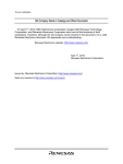
The MC68838 media access controller (MAC) chip implements the MAC protocol for a
station operating under the ANSI standard for FOOl LANs (see Figure 1-1). FOOl is a
125-Mbitlsec, fiber-optic-based token ring designed to accommodate rings up to 1000
stations, 2 km between stations, and 200-km total ring length.
USER SYSTEM BUS
r - - - - - - - - - - ~+-~I
OPTIONAL
-I
I
~ __ ~~~R~A:~~M___ :
AMPLIFIER
FCG • MC68836
FROM FIBER-OPTIC CABLE
Figure 1-1. Motorola FOOl Architecture
The ANSI standard specifies the data link MAC layer, the physical and physical-mediadependent entities, and the station management and submanagement physical
connection management.
The MAC protocol, the lower sublayer of the data link layer, provides for fair and
deterministic sharing of the physical medium, address recognition, FCS generation and
verification, frame insertion, frame repetition, frame removal, token generation, and
certain error recovery procedures.
MOTOROLA
MC68838 USER'S MANUAL
1-1
1.1 OVERVIEW
II
The MAC chip transmits information to and receives information from the physical layer
as a symbol pair every 80 ns, where a symbol is either a nibble (4 bits) of data or a
control symbol. It does this using separate transmit and receive buses, each composed
of 10 data signal lines. Transfers on the FSI transmit and receive buses are synchronous
with the 80-ns clock (BYTCLK). The MAC chip also has an NPI enabling an external
processor to read and write registers,which allows the processor full control of
management facilities.
1.2 CHIP FEATURES
The following is a list of the MAC chip's features:
• Completely Implements the ANSI FOOl MAC Standard
• Independent Receive and Transmit Oata Paths and State Machines Can
Simultaneously Generate and Check CRC
• Supports 16-Bit and 48-Bit Individual Station Addresses On Chip
• Contains an Interface to a CAM for Individual and Multicast Address Recognition
• Supports Several Bridging Facilities:
-
Can Reverse Bit Ordering on OA and SA
-
Contains Count and Void Frame Bridge Stripping Algorithm On Chip
-
Allows Generating Frame CRC on per Frame Basis
-
Supports A and C Bit Handling for Transparent Bridging Mode
-
Supports Extended Address Recognition Timing for Address Recognition
• Supports Optional FOOl Standard Capabilities Such As:
-
Receipt of Additional Frame Status Indicators
-
Restricted Tokens
-
Synchronous Frames
• On-Chip Counters Support Station and Network Management Functions
-
Token Counter
-
Frame Counter
-
Last Frame and Error Counter
-
Void Timer for Latency Calculations
• Contains an NPI
• Contains Extensive Self-Test Capabilities, Scan Path Logic, and Data Parity
Generation and Checking
• High-Speed CMOS Technology
1-2
MC68838 USER'S MANUAL
MOTOROLA
SECTION 2
FUNCTIONAL DESCRIPTION
There are four functional logic domains in the MAC chip: the NPI, the receive data path,
the transmit data path, and the clock and test logic.
2.1 NODE PROCESSOR INTERFACE LOGIC
The function of the NPI is to provide amechanism for an external processor to control the
MAC chip and receive status information and interrupt notifications. The NPI contains the
global command/status registers, an address decoder, the data latches, and the
controlling logic.
The NPI has an address bus with an associated read/write line and a bidirectional 16-bit
data bus. An interrupt line can notify an external processor of the occurrence of some
event.
2.2 RECEIVE DATA PATH
The receive data path is the internal data bus associated with receiving packets from the
ring. It connects to the external RCDATx bus (data bus from the ELM chip) through a
pipeline latch in the receive latch logic and to the RPATHx (data bus to the FSI chip).
Only the receive data latch containing the current received symbol pair drives this
internal data bus. Usually several different logic blocks are concurrently reading and
processing this symbol pair. These logic blocks perform the following functions:
• Decode the input symbol pair, recognize the beginning of frames, and use this
information to run the receiver FSM.
• Compare the DA field of a received packet to this station's individual 16- or 48-bit
address.
• Compare the SA field of a received packet to this station's individual 16- or 48-bit
address.
• Run the external CAM address matching logic.
• Compare the INFO field of claim frames to this station's requested token rotation
time.
• Perform CRC checking on the received packet.
• Store the frame status indicators that have been received.
• Keep a count of the number of good and bad frames received.
MOTOROLA
MC68838 USER'S MANUAL
2-1
IJ
2.2.1 Receive Latch
The receive latch clocks data from the ELM chip. The data signals are latched by using
an internal clock, SAMPlE_ClK (see SYMClK description in Section 4, Signal
Description). The latched data signals are then relatched by BYTClK to provide stable
symbols for MAC processing.
II
MAC-FSI RECEIVE
SIGNALS
CLOCK SIGNALS
NODE PROCESSOR SIGNALS
ADDRESS
COMPARE
MAC-FSI TRANSMIT
SIGNALS
I
I
I
------ ....
SEND
FRAME
RECEIVE
FSM
CAPTURE
TOKEN
COUNTERS
-----,
I
I
I
I
I
SENT
COUNT
1
------'I
TRANSMIT
FSM
I
I
I
1___ -
RECEIVE
CRC
CHECKER
TRANSMIT DATA LATCH
r------------------------------
MAC-PHY RECEIVE
SIGNALS
TEST SIGNALS
MAC-PHY TRANSMIT
SIGNALS
Figure 2-1. MAC Block Diagram
2-2
MC68838 USER'S MANUAL
MOTOROLA
2.2.2 Receive CRC Checker
This logic block checks the FCS field of received frames and operates a byte at a time,
using the data symbol pair currently on RCDATx. The CRC checker receives a signal
from the receiver FSM telling it when to initialize for another CRC check and receives a
strobe from the receiver FSM for each symbol pair to be included in the CRC check. This
chip provides a valid CRC signal to the receiver FSM. This signal should only be
examined after the CRC checker has processed the last byte of the incoming frame's
FCS field.
2.2.3 Sent Count
Sent count is used in bridgestrip mode to determine if a frame was sent by this station.
All data frames, as well as special void frames, are counted.
2.2.4 Counters
This block holds the following counters:
• Frame_Ct is a 16-bit unsigned count of the number of frames (good or bad) that
have been received since the last time this counter was read and reset or the chip
was reset.
• Error_Ct is a 6-bit unsigned count of the number of error frames (Le., frames
containing a bad CRC or an invalid data length) that were detected by this station,
but by no previous station, since the last time this counter was read and reset or the
chip was reset.
• Lost_Ct is a 6-bit unsigned count of the number of frame format errors that have
occurred since the last time this counter was read and reset or the chip was reset.
• Token_Ct is a 16-bit unsigned integer.
These counters do not stick at their largest value, but alway? wrap around to zero. These
registers receive their increment signals from the receive FSM.
2.2.5 Receive Finite State Machine
This FSM implements the receiver process as described in the FDDI MAC standardi.e., it controls all aspects of parsing and validating frames and tokens, determines
whether a frame should be received or stripped, detects ring errors, and notifies the
transmit FSM of any relevant events. This block also decodes and forwards the received
FC field, decodes the current symbol pair on the receive data path, and parses and
forwards the received frame status field. This block interprets all the status flags
described in the MAC standard: E_FLAG, A_FLAG, C_FLAG, N_FLAG, and R_FLAG.
MOTOROLA
MC68838 USER'S MANUAL
2-3
_
IliI
2.2.6 Address Comparator
This block performs part of the DA actions, SA actions, and CT actions as specified in the
FOOl MAC standard. Specifically, this block compares the OA and SA fields of received
frames to this station's individual addresses (my short address register and my long
address register). It also compares the INFO field of received claim frames (the token
rotation time requested by another station) to this station's desired token rotation time.
This logic block has two parts:
1. A register array that contains this station's individual 16- and 48-bit address (my
short address register and my long address register) and this station's desired
token rotation time. This register block contains a byte-wide read-only port that
feeds into the comparator and into the transmit data path when generating claim,
beacon, and void frames.
2. The comparison logic part that contains a byte-wide comparator that gets its inputs
from the register array and from the receive data path).
The receive FSM controls this logic, and the results of the comparison are passed to the
receive FSM.
2.2.7 Receive Host Interface
The FSI receive logic controls the RPATHx bus and RCCTLx bus that pass received
frames to the FSI. It strips off the delimiters before passing the frame to the FSI. It
handles all the extra control and handshake lines required for the RPATHx bus. The
receive FSM controls this logic and receives abort/flush signals from it. The system
interface receive logic is completely separate from, and does not communicate with, the
system interface transmit logic.
2.3 TRANSMIT DATA PATH
The transmit data path is the internal data path associated with the transmission of data
onto the ring. The send frame logic assembles a packet consisting of preamble (idles),
JK, FC, OA, SA, INFO field, CRC, T, and the FS indicators from various sources.
Frame_Data is multiplexed with either idles or repeat data from the receive data path in
the transmit latch logic. The transmit latch logic contains the TXDATx pipeline latch that
drives the TXDATx external bus. The TXDATx external bus passes a symbol pair to the
ELM chip on the following BYTCLK cycle after the MAC chip has received it.
2-4
MC68838 USER'S MANUAL
MOTOROLA
Frame data at the transmit latch logic can have anyone of the following sources:
• The transmit data path latch, which contains the symbol pair passed from the FSI via
the external TPATHx bus. This latch is part of the FSI TX interface logic.
• The delimiter generator, which transmits frame delimiters like idles, J, TT, etc., in
response to requests from the transmit FSM.
• The transmit CRC generator, which appends the frame check sequence to the end
of the data field.
• The address registers, which hold this station's individual addresses and its value of
desired token rotation time for void, claim, and beacon frames. These registers are
properly a part of the receive data logic but can be accessed by the transmit data
logic as needed.
2.3.1 Transmit Data Host Interface
The FSI logic controls, the TPATHx bus over which the FSI passes packets to be
transmitted to the MAC. This logic handles all the extra control and handshake lines
required for the TPATHx bus. For example, it controls the reception of packet request
information from the FSI, the notification that the MAC is ready for the next packet or
packet request header, etc. This logic does not communicate with the FSI receive logic.
2.3.2 Send Frame Logie
The send frame block is responsible for the actual transmission of a frame including the
sequencing and sending of (i.e., multiplexing of) the preamble, the appropriate
delimiters (e.g., JK, TR, RR, etc.) the FC field (for token, claim, beacon, and void frames),
the OA and SA fields (for claim, beacon, and void frames where they could be my long
address register, broadcast or null address), information fields (claim and beacon
frames), general data (FC, SA, OA, and INFO fields for FSI frames), the CRC field, and
the requested frame status. The transmit FSM tells this logic what kind of frame to send
and when to start sending it.
2.3.3 Capture Token Logic
This logic block holds the packet request header passed to it by the FSI. The packet
request header contains all the information that the MAC transmitter needs to determine
when it can send this frame (Le., asynchronous/synchronous, token type, immediate
mode or not, etc.), what type of token to issue later, whether a CRC is to be generated,
etc. In addition to parsing this information, this block contains the logic to determine
when a token can be captured and issued and when a frame can be transmitted. It feeds
these signals into the transmit FSM that takes the appropriate action depending upon its
current state.
MOTOROLA
MC68838 USER'S MANUAL
2-5
2.3.4 Transmit CRC Generator
fI
This logic block appends the FCS field (a 32-bit CRC) onto transmitted frames. Some
packets may already contain the FCS field, in which case this logic block may be used
as a CRC checker instead of a CRC generator. When used as a checker, a bit is set in
the interrupt event register when the transmitted CRC field is incorrect. This causes an
interrupt if this event is not masked in the interrupt mask register. This logic block
computes the CRC on data bytes it reads from the FRAME_DATA bus that come from the
send frame block. It also receives control signals from the transmit FSM.
2.3.5 Transmit Finite State Machine
The transmit FSM implements the transmit process as described in the FOOl MAC
standard. Specifically, the transmit FSM repeats packets from other stations on the ring,
determines when it can capture the token, how long it can hold the token, what type of
token to issue, what kind of frame to send (but does not actually send it), and participates
in the ring recovery procedures, etc.
2.3.6 Timers
This logic block contains all the MAC protocol timers (TRT, THT, and TVX timers), the
associated register fields used to load them (T_Max, TRT time remaining register,
T_BID_RCIT_INFO, and TVX_Value), and the LATE_CT. The MAC standard specifies an
additional register, T_apr, which can contain redundant information and therefore is not
implemented.
The TVX timer is used to ensure that a good frame (Le., correct CRC and valid data
length) or a nonrestricted token is seen by this station on every regular basis. It can be
used to detect events such as a babbling station, an infinitely circulating restricted token,
a lost token, etc.
The TRT timer is used to determine the time taken for each rotation of the token. The
transmit FSM uses this information to decide whether the token has been lost and
whether this station can then transmit when it receives the token. If the token takes too
long to get to this station, it implies that the ring is busy and this station may have to defer
its lower priority transmission. This timer also times the claim and beacon recovery
procedures to determine if they will complete.
The THT timer controls the length of time that a station can transmit when it has captured
the token. This timer is loaded with the value of the TRT timer when a token is captured.
A station can then transmit asynchronous frames until this timer expires. This procedure
ensures that the sum of this station's transmissions and that of the previous station's
transmissions during this rotation of the token are (approximately) less than the mutually
agreed upon token rotation time.
2-6
MC68838 USER'S MANUAL
MOTOROLA
This logic block is connected to the receive data path to be able to load a bid time
register from claim frames that are being received. In addition, it receives signals to
enable/disable the TVX timer and to reset the TVX timer from the receiver FSM. Its only
outputs (other than to the NPI) are TRT expired, TVX expired, THT expired, and
LATE_CT equals zero interrupts.
2.3.7 Transmit Data Latch (and Repeat Function)
This logic block contains the repeat function and multiplexes the repeat path with
FRAME_DATA from the send frame logic block. The repeat function reads symbol pairs
from the receive data path and repeats them to the ELM. Usually this logic transmits the
symbol pair just received, but when receiving the FS indicators, the logic may need to
modify the received Rand S symbols according to the values in the frame status logic
and the values in the register associated with repeating additional FS symbols. Also, this
logic selectively replaces the last symbol pair with an IDLE symbol pair when a frame is
detected as a fragment.
2.4 TEST AND CLOCK LOGIC
The MAC supports complete boundary scan testing and random access reading of
almost all of the internal chip state through the NPI. Boundary scanning means that
every signal on this chip (other than the MATCH signal, the test signals, and clocks) has
an associated scan latch that enables the testing interface to serially shift in an arbitrary
bit pattern to be used for the corresponding input or output signal and to shift out the
values of these signals while holding the clock. The MAC also has a built-in self-test
capability.
MOTOROLA
MC68838 USER'S MANUAL
2-7
IJ
2-8
MC68838 USER'S MANUAL
MOTOROLA
SECTION 3
REGISTER DESCRIPTION
There are 36 user-visible control/status registers. The registers, which are accessible
through the NPI, are summarized in Table 3-1. When there is an A and B version of a
register, the A part holds the least significant bits, and the B part holds the most significant
bits. The first hex digit of the address refers to NPA5-NPA4, and the second hex digit
refers to NPA3-NPAO.
MOTOROLA
MC68838 USER'S MANUAL
3-1
II
Table 3-1. MAC Registers
Register Name
II
Mnemonic
NPA5-NPAO No. of
Hex
Bits
Type
00
16
ReadlWrite
Control Register A
MAC_CNTRL_A
Control Register B
MAC_CNTRL_B
01
16
ReadlWrite
Interrupt Mask Register A
INTR_MASK_A
02
16
ReadlWrite
Interrupt Mask Register B
INTR_MASK_B
03
16
ReadlWrite
Interrupt Mask Register C
INTR_MASK_C
04
16
ReadlWrite
My Short Address Register
MSA
10
16
Read/Cntl Write
My Long Address Register A
MLA_A
11
16
Read/Cntl Write
My Long Address Register B
MLA_B
12
16
Read/CnU Write
My Long Address Register C
MLA_C
13
16
Read/CnU Write
Target Request Time Register
T_REQ
14
16
Read/CnU Write
TVX, TRT Initial Timer Parameter Register TVX_VALUE & T_MAX
15
16
Read/Cntl Write
Revision Number Register
REV_NO_REG
1C
12
Read-Only
Void Time Register
VOID TIME
1E
16
Read-Only
Token Count Register
TOKEN_CT
1F
16
Read-Only Clear
Frame Count Register
FRAME_CT
20
16
Read-Only Clear
Lost and Error Count Register
LOST_CT & ERROR_CT
21
12
Read-Only Clear
Interrupt Event Register A
INTR_EVENT_A
22
16
Read-Only Clear
Interrupt Event Register B
INTR EVENT B
23
16
Read-Only Clear
Interrupt Event Register C
INTR_EVENT_C
10
3
Read-Only Clear
Receive Status Register
RX_STATUS
24
16
Read-Only
Transmit Status Register
TX_STATUS
25
16
Read-Only
TRT Time Remaining Register A
T_NEG_A
26
16
Read-Only
TRT Time Remaining Register B
T_NEG_B
27
8
Read-Only
Information Field Register A
INFO_REG_A
28
16
Read-Only
Information Field Register B
INFO REG B
29
16
Read-Only
BIST Signature Register
BIST_SIGNATURE
2A
16
Read-Only
TVX Timer Register
TVX_TIMER
2B
16
Read-Only
TRT Timer Register A
TRT_TIMER_A
2C
16
Read-Only
TRT Timer Register B
TRT_TIMER_B
20
8
Read-Only
THT Timer Register A
THT_TIMER A
2E
16
Read-Only
THT Timer, Sent Count Registers
SENT COUNT &THT TIMER B
2F
16
Read-Only
Packet Request Register
PKT_REQUEST
30
16
Read-Only
Receive CRC Register A
RC_CRC_A
31
16
Read-Only
Receive CRC Register B
RC CRC B
32
16
Read-Only
Transmit CRC Register A
TX CRC A
33
16
Read-Only
Transmit CRC Register B
TX_CRC_B
34
16
Read-Only
3-2
MC68838 USER'S MANUAL
MOTOROLA
3.1 REGISTER TYPES
The following paragraphs discuss the different types of registers used in the MAC.
3.1.1 Read/Write Registers
These registers can be read and written by the NP at any time. Usually, these registers
cannot be modified by the MAC chip. The only exceptions are the RESET_FIELD and
FOX_MODE bits in control register B. These registers are all cleared by power-up reset
(see Section 4 Signal Description for a description of the PWRUP pin). Most bits in these
registers are unaffected by a MAC_Reset.
3.1.2 Read/Control Write Registers
These registers can be read by the NP at any time but can be written only when the MAC
FSMs are turned off (see MAC_ON bit in the control register A). These registers hold chip
parameters that the MAC needs before it can operate correctly. The NP should write these
registers before BIST is run. These registers cannot be modified by the MAC chip. All
these registers are cleared by power-up reset but are unaffected by a MAC_Reset.
3.1.3 Read-Only/Clear Registers
These registers can be read by the NP at any time (like all registers) but can never be
written by the NP (even in test mode). Unlike read-only registers, these registers are
automatically cleared when read by the NP. If the MAC chip tries to modify a register that
is being accessed by the NP, the register is cleared and the MAC writes the new updated
state. The MAC chip can change these registers at any time, even when the MAC FSMs
are turned off. These registers are all cleared by power-up reset.
3.1.4 Read-Only Registers
These registers can be read by the NP at any time but can never be modified by the NP.
The MAC chip can change these registers at any time, even when the MAC FSMs are
turned off. Generally, they are undefined after power-up reset.
The first six of these read-only registers (24-29 hex) are the only ones that are of interest
to general-purpose software. Through the remaining registers, the user can access almost
all MAC internal states. Access to these registers is essential for both ATE testing and
board-level diagnostics. Many of these registers hold part of an internal 24- or 32-bit
register that can change on each BYTCLK. Since only one register can be read at a time,
it may be difficult for an NP to obtain a consistent value of the internal register without
stopping BYTCLK.
Whenever the NP attempts to read a nonexistent register, the MAC chip completes the NP
read cycle normally (returning a valid, though unpredictable value) and records the
erroneous event by setting the NP_ERR bit in the interrupt event register B.
MOTOROLA
MC68838 USER'S MANUAL
3-3
II
Whenever the NP attempts to write to a nonexistent register, a read-only register, a readonly/clear register, or a read/control write register when the FSMs are on, then the MAC
completes the NP write cycle normally (though no registers are modified) and records the
event by setting the NP_ERR bit.
A" unused bits (Le., undefined bits) in the MAC registers are read as zero and are ignored
when written. However, software should always write these unused bits as zeros and
should assume that these bits have unpredictable values upon reading.
II
All timing values are stored as the unsigned twos complements of the target or as
remaining time in octets (Le., 80-ns units). Hence, the numerically greater magnitude
represents the shortest time remaining. For example, if the TVX timer has 240 ns left until
expiration, the time remaining would be three octets, and the 16-bit TVX register would
contain 1111 1111 1111 11 01.
3.2 CONTROL AND STATUS REGISTERS
There are two control registers and two status registers for receive and transmit functions.
3.2.1 Control Register A (MAC_CNTRL_A)
Control register A controls the receiver portion of the MAC and a few joint
receiver/transmitter aspects. The NP can read and write control register A at any time. The
MAC chip never modifies this register. It is cleared on power-up reset and unaffected by a
MAC_Reset.
2
14
13
12
11
10
9
8
COPY_ALL
7
6
5
4
3
2
o
MAC_aN-MAC On
This bit turns the receiver/transmitter FSM on or off. When set to one, the receiver finite
state machine transitions to the listen state (state RO) and the transmitter finite state
machine transitions to the Tx_ldle state (state TO).
0= Both the receiver and transmitter FSM are turned off. When in this state, the MAC
receiver/transmitter ignores a" inputs and stays in this state until MAC_ON is set.
When they are operating, the receiver and transmitter can be turned off at any
time by clearing this bit. (No timers are running).
1 = The receiver and transmitter finite state machines are operating and can be in
any of the states RO-R5 or TO-T5, respectively, or in the FDX states (A" timers
are running).
3-4
MC68838 USER'S MANUAL
MOTOROLA
SET_BIT5-Set Bit 5
Repeat fifth control indicator as an S-symboJ.
o = The fifth control indicator is repeated exactly as received.
1 = The repeating function always causes the fifth control indicator received to be
transmitted as an S-symbol. If the fifth received control indicator is already an
S-symbol, then the BIT5_'-SS interrupt is signaled. Nothing happens if there are
not five control indicators.
SET_BIT4-Set Bit 4
Repeat fourth control indicator as an S-symboJ.
o = The fourth control indicator is repeated exactly as received.
1 = The repeating function always causes the fourth control indicator received to be
transmitted as an S-symboJ. If the fourth received control indicator is already an
S-symbol, then the BIT4_'-SS interrupt is signaled. Nothing happens if there are
not four control indicators.
REVERSE_AOOR-Reverse the OA and SA Fields of All Frames
This bit is used by both the receiver and transmitter portion of the MAC. This bit reversal
only occurs across the FSI bus; hence, it does not affect the CRC checking/generation
nor the interpretation of the my long address or my short address registers, etc. The
order of the octets is not affected by this bit. Octets are passed to and from the FSI in
the same order as they appear on the fiber.
o = No bit reversal will occur.
1 = The MAC chip will reverse the bit order of data octets passed to and from the FSI
(Le., across RPATHx and TPATHx for all octets that make up the OA and SA
fields of all frames to be sent or received from the FSI). Therefore, for OA and SA
octets, bit (7-x) is passed to the FSI on RPATHx, and bit (7-x) is obtained from
the FSI on TPATHx.
This feature is useful when implementing 802.3 and 802.4 protocol bridges to FOOl and
vice versa.
FLUSH_SA47-Flush Source Routing Frames
0= The MAC will copy frames when the individual/group bit of the SA (bit 47 of
48-bit addresses or bit 15 of 16-bit addresses) is one.
1 = The MAC will not copy frames when the individual/group bit of the SA (bit 47 of
48-bit addresses or bit 15 of 16-bit addresses) is one.
This bit has no effect on the ring protocols. In particular, it does not change the frame
stripping algorithms nor affect whether a claim frame is higher or lower. When
comparing the SA of a received frame to the my long address register, the I/G of the
received SA and the my long address register are ignored-i.e., the I/G bit of the
received SA is always considered a match, regardless of the value of FLUSH_SA47 or
the my long address register. On the other hand, bit 47 of the my long address register
is used for OA matches. FLUSH_SA47 has no effect when COPY_ALL is 10 or 11 or
when NSA frames are received (i.e., NSA source routing frames will still be received).
The current ANSI MAC standard requires the individual/group bit of the SA to be zero.
MOTOROLA
MC68838 USER'S MANUAL
3-5
II
II
COpy_ALL-Copy All
This bit copies or passes extra frames and fragments to the FSI. The only frames that
are copied are LLC, SMT, implementor, and reserved frames. COPY_ALL is intended
for use in monitor and analyzer stations.
00 = The MAC attempts to copy all LLC, SMT, reserved for implementor, and
reserved for future standardization frames that have valid length, whose DA is
matched, whose SA is not matched (subject to COPY_OWN) or is an NSA
frame, and is not a secondary NSA frame.
01 = The MAC additionally copies MAC and void frames that: have valid length,
whose DA is matched, and whose SA is not matched (subject to COPY_OWN).
10 = The MAC additionally copies tokens and frames that: are too short (but with an
even number of data symbols), whose DA is not matched, or whose SA is
matched.
11 = The MAC additionally copies fragments, format errors, and frames with an odd
number of data symbols.
When COPY_ALL = 10 or 11, the MAC will still flush (not copy) secondary NSA frames
if COpy_EXTRA_SMT = 00. Only monitor systems should set COPY_ALL to 10 or 11.
COPY_OWN-Copy Frames Sent by This Station
The MAC chip ignores this bit when COPY_ALL = 11 or 10 or if the received frame is an
NSA frame. The COPY_OWN mode of operation is not intended for normal operation
but is reserved for special monitor stations and for ring loopback tests applicable to all
stations.
o = The MAC does not copy frames that it is currently sending nor frames that it
believes it previously sent, even if the MAC is requested to copy all frames with a
certain FC or DA (see the following register fields).
1 = The MAC copies frames whose SA is matched if the frame would be copied
otherwise and other frames only if the frame is directly addressed to the station.
(DA = broadcast, my long address register, or my short address register.)
COpy_EXTRA_SMT-Copy Certain Extra SMT Frames
When COPY_ALL = 11 or 10, this bit field is ignored (except that secondary NSA frames
are still flushed when COpy_EXTRA_SMT = 00). This bit field does not affect how the
MAC sets the A and C control indicators.
00 = The MAC copies valid SMT frames if the DA is matched and the frame is not a
secondary NSA frame and the SA is not matched or the frame is a primary NSA
frame.
01 = The MAC additionally copies secondary NSA frames whose DA is matched.
10 = The MAC additionally copies all NSA frames or 48-bit group-addressed SMT
frames whose SA is not matched (subject to COPY_OWN).
11 = The MAC additionally copies all NSA frames or 8-bit addressed SMT frames
whose SA is not matched (subject to COPY_OWN).
3-6
MC68838 USER'S MANUAL
MOTOROLA
COPY_IND_LLC-Copy All Individual LLC Frames
This bit does not affect how the MAC sets the A and C control indicators.
0= The MAC copies individually addressed LLC frames if the DA is matched (subject
to the COPY_OWN bit). The MAC chip ignores this bit when
COPY_ALL = 11 or 10.
1 = In addition to the frames it is already copying, the MAC copies all LLC,
implementor, and reserved frames whose DA field indicates a 48-bit individual
address. The MAC will not copy LLC frames it sent unless COPY_OWN = 1.
COpy_IND_LLC is primarily used for promiscuous bridges.
COpy_GRP_LLC-Copy All Multicast LLC Frames
This bit does not affect how the MAC sets the A and C control indicators.
0= The MAC copies multicast LLC frames if the DA is matched (subject to
COPY_OWN) in the CAM. The MAC chip ignores this bit when the
COPY_ALL = 11 or 10.
1 = In addition to the frames it is already copying, the MAC copies all LLC,
implementor, and reserved frames whose DA field indicates a 48-bit group
address. The MAC will not copy group LLC frames it sent unless
COPY_OWN = 1.
COpy_GRP_LLC is primarily used for promiscuous bridges.
II
DSABL_BRDCST-Disable Broadcast
0= The MAC treats broadcast frames normally (as described in the FDDI standard).
This bit does not affect the behavior of SMT frames-i.e., SMT broadcast frames
are always recognized and copied. Unlike many register bits, this bit still has an
effect when COPY_ALL = 11 or 10. Specifically, this bit affects the OD field of an
END_DATA transfer for received broadcast frames.
1 = The MAC treats a MAC, LLC, implementor, or reserved broadcast frame (Le., DA
is all ones) exactly as if it were another multicast frame of the same frame type.
Hence, an LLC broadcast frame is recognized and copied only if the broadcast
address is found in the CAM or COPY_GROUP_LLC = 1 (subject to
COPY_OWN). The A_FLAG and C_FLAG are only set if the broadcast address is
found in the CAM since COPY_GROUP_LLC has no effect on these indicators.
RUN_BIST-Run Built-In Self-Test
o = The MAC operates normally.
1 = The MAC runs its internal BIST. To run BIST properly, the MAC_ON and
RUN_BIST bits must both be cleared for at least five BYTCLK cycles, and then
both bits must be set simultaneously. During BIST, the MACINT line is only
asserted when the BIST has finished (after 65535 BYTCLK cycles), at which time
the BIST signature register is frozen. The actual signature depends on the values
of each of the writable or clearable registers, except the interrupt mask and
interrupt event registers. In addition, the signature also depends upon the value of
the MATCH and RABORT pins (usually negated during BIST). MTESTx should
be 00. Also, the TXPARITY_ON bit should be 0; otherwise, the parity of the nine
MOTOROLA
MC68838 USER'S MANUAL
3-7
lines (TPATHx and TPRITY) will affect the SIST. SYMCLK, RCDATx, and
TXCTLx have no effect during BIST.
RXPARITY-Generate Odd or Even Receive Parity
0= The MAC generates RPRITY so that RPRITY and RPATHx have odd parity.
1 = The MAC generates RPRITY so that RPRITY and RPATHx have even parity.
II
NTE-.AL_FRM8-Note All Frames
o = The MAC sets the FRAME_RCVD bit in the interrupt event register only when the
frame count register overflows (i.e., potentially notifies the NP for every 65536
frames). It is possible, though unlikely, for the DOUBLE_OVF bit not to be set
when FRAME_CT overflows. Therefore, NTE_AL_FRMS should not be set
unless the NP can read the FRAME_CT before it can overflow or unless precise
frame counts are not required.
1 = The MAC sets the FRAME_RCVD bit in the interrupt event register when the
FRAME_CT is incremented.
3.2.2 Control Register B (MAC_CNTRl_B)
Control register B controls the MAC transmitter. The NP can read and write this register at
any time. The MAC chip only modifies the RESET_FIELD bits. The register is cleared on
power-up reset and is unaffected by a MAC_Reset.
15
14
13
12
11
10
9
8
RESETJIELD
7
6
5
4
3
2
o
RING_PURGE-Enable Ring Purging Mode
This bit is ignored by the MAC when RING_OPERATIONAL is low or cleared or when
the chip is in the FDX states. Unlike BRIDGE_STRIP, RING_PURGE does not affect
frames the MAC thinks it sent and hence packets the MAC asks the FSI to flush (not
copy). Consequently, it is useful to set both BRIDGE_STRIP and RING_PURGE.
There is typically only one purging station per ring. The choice of the ring purger, if any,
is beyond the scope of the FDDI standard.
o = The MAC operates normally.
1 = The MAC purges the ring upon every token rotation until the NP resets this bit.
The MAC performs the following operations:
Captures every token (unless RING_OPERATIONAL is zero),
Sends any FSI frames for which the token is usable,
Sends two special void frames (see the BRIDGE_STRIP bit description), and
Releases the token.
3-8
MC68838 USER'S MANUAL
MOTOROLA
The kind of token released is specified by the token send field in the packet
request header of the last FSI frame sent with this token, or is the kind of token
captured if no FSI frames were sent. The MAC then purges all frames until one of
the following occurs:
A special void frames returns,
A nonduplicate token returns,
RING_OPERATIONAL becomes low,
The transmitter enters the FDX states, or
The MAC is turned off (MAC_ON = 0).
Purging does not stop if a duplicate token is received (Le., a token received while
transmitting). Purging differs from stripping in that purging creates no frame
fragments.
FDX_MODE-Enable Full-Duplex Operation
o = The transmitter operates purely in ring mode.
1 = The next time the transmitter enters the Tx_ldle (TO) state, it transitions to the
FDX_ldle state. The transmitter then alternates between the FDX_ldle and
FDX_Data states, depending on whether or not there is a frame to send. The
transmitter leaves FDX_ldle or FOX_Data upon:
Receiving a higher or lower claim frame,
Receiving any beacon frame,
Receiving a MAC_RESET (RESET_FIELD <> 00), or
Clearing this bit, which puts the transmitter in the FDX_ldle state.
RING_OPERATIONAL (which could be either zero or one) is ignored while in the
FDX states. RING_OPERATIONAL is cleared upon leaving the FDX states
unless these states are left because FDX_MODE is cleared.
FOX_MODE is useful in implementing point-to-point links and for diagnostics.
BRIDGE_STRIP-Use Bridge/Switch Stripping Algorithm
o = The normal stripping algorithm is used, based upon matching the SA against my
short address register, my long address register, and the CAM entries.
1 = An additional stripping occurs when the count of frames sent minus frames
received (called SENT_COUNT) is greaterthan zero. SENT_COUNT is also
cleared (hence, stripping stops) when:
A special void frame (FC = 48-bit addressed void frame) is received.
Individual DA is matched (A_FLAG = 1 and the I/G bit of the DA = 0).
SA is matched (M_FLAG = 1-Le., SA = my long address register and
SA<> nUll) and frame has a valid CRC, length, and E-indicator (E_FLAG = O.
A claim frame is received.
A beacon frame is received.
A token is received.
MOTOROLA
MC68838 USER'S MANUAL
3-9
II
II
The SENT_COUNT is not cleared (stripping continues) if a duplicate token is
received (Le., a token received while transmitting).
When this bit is one, the MAC transmitter internally creates and transmits one
special void frame after leaving the TX_Data state (Le., just before it would
normally release the token). This MAC chip always creates and transmits a
special void frame with the following characteristics:
FC = 48-bit addressed void frame
DA = my long address register
SA = my long address register
Zero INFO bytes
FCS = valid CRC
EFS = TRRR.
When RING_OPERATIONAL is zero, this bit is ignored by the MAC chip.
TXP ARITY_ ON-Transmit Parity Check On
0= The TPRITY input in the TPATHx bus is ignored.
1 = TPATHx and TPRITY together must have odd parity (Le., an odd number of the
nine lines must be high), or the MAC aborts the transmission of this frame and
asserts TABORT.
REPEAT_ONLY-Repeat Only
The transmitter cannot capture the token.
o = The transmitter operates normally.
1 = The MAC will not start sending any more frames from the FSI, although it can
finish any frames it has started to send as well as sending any frames internally
generated by the MAC (Le., claim, beacon, and void frames). Specifically, the
conditions USABLE_TOKEN and ANOTHER_FRAME are always zero; thus, the
transmitter cannot capture a token. If it has the token, it cannot send any more
frames although it can finish sending the frame it is currently sending (plus any
associated token). The transmitter cannot start sending frames whose
TOKEN_TYPE field in the packet request header allows the frame to be sent
without a token. When REPEAT_ONLY = 1 and RING_PURGE = 1, the MAC will
still capture the token, send two special void frames, and then release the same
kind of token.
3-10
MC68838 USER'S MANUAL
MOTOROLA
LOSE_CLAIM-Lose Claim
The transmitter always loses the claim bidding process.
o = The transmitter works normally.
1 = The transmitter treats all Lower_Claim frames as Higher_Claim frames and all
My_Beacon frames as Other_Beacon frames (the receiver operation is
unaffected). All other Recovery_Required conditions are ignored (Le., TVX
expiration, TRT expiration when LATE_CT> 0, and T_Opr < target request time
register when RING_OPERATIONAL is one) while in any of the states from which
the Recovery_Required transitions originate (Le., Tx_ldle, Tx_Repeat, Tx_Data,
Tx_Token, or Tx_Void states). Because the Recovery_Required transitions
cannot occur, the transmitter will never enter the Tx_Claim or TX_Beacon states,
except upon a MAC_RESET/CLAIMING, MAC_RESET/BEACONING, or upon
TRT expiration while already in Tx_Claim (MAC then goes to Tx_Beacon).
However, once it is in these states (e.g., if this bit is set while in Tx_Claim), the
MAC can stay in any of these states.
RESET_FIELD-Reset Field
This field, which includes various types of MAC resets, is used to apply general signals
to the whole of the chip. The idea of a signal is that it only lasts for a single BYTCLK
cycle, unlike the regular control bits whose effect continues as long as the bit is set.
00 = Normal operation and no MAC_RESET occurs.
01 = A reguiar FDDI-specified MAC_RESET occurs.
10= A combined MAC_RESET/BEACONING action occurs (Le., a MAC_RESET
followed by the transmitter going to the Tx_Beacon state). This action is
equivalent to an SA_MA_CONTROL request (beacon) service primitive.
11 = A combined MAC_RESET/CLAIMING action occurs (Le., a MAC_RESET
followed by the transmitter going to the Tx_Claim state).
When the MAC is off (MAC_ON = O), this bit field retains its last written value (Le., it is
not cleared upon the next rising edge of BYTCLK), and it has no effect until the MAC is
subsequently turned on.
FSLBEACON-Transmit Beacons from the FSI
o = If FSLBEACON is zero, there are no queued FSI frames, or the BCN_FRAME bit
of the queued frame is zero, then the MAC sends internally created beacon
frames with an INFO field consisting of four bytes of zeros (Le., BEACON_TYPE
is unsuccessful claim). The MAC will not attempt to skip over FSI generated
frames whose BCN_FRAME is zero to find later frames with a BCN_FRAME of
one. Also, a frame with a BCN_FRAME of one will only be sent once. Hence, for
the MAC to continue to send FSI generated beacon frames, new frames need to
be continually queued up to the MAC chip.
1 = The MAC allows the FSI to send beacon frames that have been generated by
upper level software. Whenever the MAC is in the beacon state (T5), a frame is
available to transmit at the MAC/FSI interface, and the BCN_FRAME bit is set in
its packet request header, the MAC will send this frame.
MOTOROLA
MC68838 USER'S MANUAL
3-11
II
The FSLBEACON bit has no effect unless the MAC chip is in the beacon state (state
T5). Also, when FSLBEACON is one, only the BCN_Frame, Append_CRC, and
Extra_FS fields of the packet request header have any effect. The FC and address fields
of the frames sent from the FSI are not checked in any way, though a bad CRC will still
generate the BAD_CRC_SENT interrupt.
II
DELAY_TOKEN-Wait for FSI Data while Holding the Token
o = When this bit is zero or the M_BIT is zero, then the MAC ensures that exactly
eight idle symbol pairs of preamble are sent between the ending delimiter of the
last frame and the starting delimiter of the following frame or token. If the last
frame transmission was aborted (Le., no ending delimiter sent), then zero, one, or
two additional idle symbol pairs may be sent, as measured from the last data
symbol pair sent.
1 = The MAC waits up to an additional 32 cycles (a cycle is 80 ns) for the FSI to
transfer a new Tx_Start after a Tx_End transfer (see 8.1 Transmit Data Path
Control) before it releases the token. Specifically, if this bit is one and the M_Bit
of the last Tx_End transfer is one, then the MAC waits as long as it can, while still
guaranteeing that it will transmit no more than 40 idle symbol pairs of preamble
between the ending delimiter of the last frame and the starting delimiter of the
following frame or token.
This function allows for slower delivery of the start of frame data at the MAC-FSI
interface.
IGNORE_SACAM-Ignore Source Address CAM Recognition
If EXT_DA_MATCH is set, then this bit is ignored.
0= If the MATCH signal is asserted in the second cycle immediately following the last
byte of the SA, then (assuming no special copy modes are set) the SA is stripped
and the frame is flushed.
-::--::--::-=-=-:-:1 = The MAC ignores the MATCH signal in determining whether the SA matches or
not.
EXT_DA_MATCH-Extended Destination Address Match Control
o = DA and SA match. Flush the frame currently being received after the second
byte of the SA if the MATCH signal was not asserted, my long address register or
my short address register was not recognized, or the MAC is not in promiscuous
mode. (The LDADDR pin is an output signaL)
1 = Extended DA match allows the user to delay asserting the MATCH or
TR_BR_FWD signals up to and including the last byte of the FCS. The packet can
be flushed at any time by asserting RABORT. SA_CAM match is not available
with this option. (The LDADDR pin becomes an input signal, TR_BR_FWD. This
signal is the power-up condition, extended DA match, and TR_BR_FWD input.)
This bit is set on power up.
To use the LDADDR pin in normal mode, the user (initialization firmware) must clear this
bit.
3-12
MC68838 USER'S MANUAL
MOTOROLA
RABORT2-ADDR16 or RABORT2 Signal Selection
0= ADOR16 pin operates as ADOA16, an output, as defined in the signal definitions.
1 = ADOR16 pin operates as RABORT2, an input, with the same functionality as the
RABORT input pin-that is, it signals the MAC that the incoming frame should be
aborted. RABORT2 is internally ORed with RABORT.
This bit is set on power up.
To use the ADOR16 signal, the user (initialization firmware) must clear this bit.
MAC_MOOE_CTL-MAC A and C Frame Status Bit Handling Option
This bit defines how the MAC sets, resets, or repeats the C-indicator bit when RABORT
or RABORT2 occurs while the MAC is receiving a frame addressed to itself or
recognized as receivable by itself.
o = Option 1. Set the A and C bits according to the MAC_MOOE_CTL = 0 functions
as defined in Table 9-1.
1 = Option 2. Set the A and C bits according to the MAC_MODE_CTL = 1 function as
defined in Table 9-1.
3.2.3 Receive Status Register (RX_STATUS)
The receive status register holds the status flags, the comparison state (e.g., the H_Flag,
L_Flag, and M_Flag), the receiver FSM state, and the decoded FC. The NP can read the
receive status register at any time but can never write to this register. It is cleared on
power-up reset and by a MAC_Reset. The flags displayed in this register are internal flags
used as described in the ANSI FOOl MAC standard.
15
14
13
12
11
10
7
6
5
4
3
2
HJLAG
9
8
o
MJLAG
RX_FSM_STATE-Receiver Finite State Machine State
This state machine controls the overall operation of the MAC receiver.
000 = Await_Sd (R1 )-Wait for JK of new frame
001 = Rc_FS (R4)-Receive and decode FS
010 = Rc_FC (R2)_Receive and decode FC byte
011 = Rc_lnfo (R3)-Receive DA, SA, INFO, and CRC
100 = Chk_TK2 (RS')-State used to repeat TT
101 = Listen (RO)-Wait for first idle
110 = Chk_TK1 (RS)-Receive TT of token
111 = Rc_Off-MAC is turned off
MOTOROLA
MC68838 USER'S MANUAL
3-13
II
R_FLAG-Current Value of R_FLAG
In general, this bit indicates whether the last token received was a restricted token or a
nonrestricted token.
o = A nonrestricted token FC is received, the MAC receiver signals the reception of a
LOWER_CLAIM, MY_CLAIM, HIGHER_CLAIM, OTHER_BEACON, or
MY_BEACON, or the MAC is turned off (MAC_ON = 0).
1 = A restricted token FC is received.
E_FLAG-Current Value of E-Flag
II
FSM_STATE-Frame State Machine State
These bits indicate the state of the frame state machine that parses the frame status field
for all frames (including those that have an odd number of data symbols).
000 = Wait_Ed-Wait for Ending Oelimiter(T)
001 = Reserved
010 = Rc_4_5-Expecting 4 and 5 Indicators
011 = Rc_A_C-Expecting A and C Indicators
100 = Rc_5_x-Expecting 5 Indicator
101 = Rc_C_4-Expecting C and 4 Indicators
110 = Wait_FS_end-Wait for End of FrameStatus
111 = Rc_E_A-Expecting E and A Indicators
N_FLAG-Current Value of N-Flag
FR_PARS_STATE-Frame Parsing State Machine State
These bits indicate the state of the frame parsing state machine that parses the OA, SA,
INFO, and CRC fields to initiate the DA_Actions, SA_Actions, and CT_Actions and
control the CAM interface signals.
000 = Parse_OA-Receiving DA
001 = Parse_SA-Receiving SA
010 = Reserved
011 = Reserved
100 = Parse_FCS-Receiving possible FCS
101 = Parse_INFO-Receiving INFO field of MAC frame
110 = Parse_Value RCV-Rest of INFO field
111 = Reserved
L_FLAG-Current Value of L-Flag
H_FLAG-Current Value of H-Flag
M_FLAG-Current value of M-Flag
A_FLAG-Current Value of A-Flag
3-14
MC68838 USER'S MANUAL
MOTOROLA
3.2.4 Transmit Status Register (TX_STATUS)
The transmit status register holds the transmit FSM state, LATE_CT,
RING_OPERATIONAL, and the state of the frame transmission machine. The NP can
read the transmit status register at any time but can never write to this register. It is cleared
on power-up reset and by a MAC_RESET.
15
12
11
7
6
10
9
8
PURGING
TX FSM STATE
5
3
2
o
II
TX_FSM_STATE-Transmit Finite State Machine State
These bits indicate the state of the overall operation of the MAC transmitter FSM.
0000 = Tx_ldle (TO)-Constantly transmit idle symbols
0001 = Tx_Data (T2)-Transmit data frames
0010 = Tx_Token (T3)-Transmit token
0011 = Tx_Void-Transmit special void frame
0100 = Tx_Repeat (T1 )-Repeat incoming frame/token
0101 = Reserved
0110= Tx_Beacon (T5)-Constantly transmit beacon frames
0111 = Tx_Claim (T4)-Constantly transmit claim frames
1000 = Reserved
1001 = Reserved
1010 = Reserved
1011 = Reserved
1100 = FOX_Oata-Transmit FSI FDX data frame
1101 = Reserved
1110= Reserved
1111 = Tx_Oft-MAC is turned off
RING_OP-Ring Operational
This value indicates whether or not the ring is operational.
0= RING_OPERATIONAL is cleared by the transmit FSM, indicating that the ring is
not operational.
1 = RING_OPERATIONAL is set, indicating that the ring is operational.
PURGING-Purging
This bit indicates the current value of purging.
1 = Transmitter is currently purging the ring. The transmitter will not enter repeat
mode (Tx_Repeat state). This bit is set upon sending the end of the first of the
two special void frames sent as a result of RING_PURGE being set.
o = A special void frame is returned or a nonduplicate token is returned,
RING_OPERATIONAL becomes zero, the transmitter enters the FOX states, or
the MAC is turned off (MAC_ON = 0). This bit is not cleared (stripping continues)
if a duplicate token is received (i.e., a token received while transmitting).
MOTOROLA
MC68838 USER'S MANUAL
3-15
FLD_SEQ_STATE-Field Sequence State
This bit controls the state of the field sequence machine that is responsible for creating
tokens, beacon, claim, and special void frames; for adding the preamble, JK, and frame
status; and for controlling the addition of the FCS to frames that the FSI passes to the
MAC for transmission.
0000 = Pre_State-Transmit preamble (idles)
0001 = Post_State-Transmit postamble (idles)
0010 = Data_FC_State-Transmit FC for data frame
0011 = Data_DA_State-Transmit DA for data frame
0100 = SD_State-Transmit JK for token/all frames
0101 = CRC_State-Transmit FCS (all required frames)
0110= Ed_State-Transmit IT (token) or TR (otherwise)
0111 = Data_State-Transmit INFO field for data frame
1000 = Data_SA_State-Transmit SA for data frame
1001 = FS_State-Transmit RR + any ExtraFS required
1010= Unused
1011 = Unused
1100 = FC_State-Transmit FC for all but data frames
1101 = Info_State-Transmit INFO (claim/beacon frame)
1110= DA_State-Transmit DA (claim/beacon/void)
1111 = SA_State-Transmit SA (claim/beacon/void)
FLD_CNT_STATE-Field Count State
These bits indicate the state of the field count machine that counts down to determine
when each of the various fields have ended and when the field sequence state machine
should proceed to its next state. In every case below, when a field has x more bytes
(really symbol pairs) to go, that count of x includes the current byte transfer. Hence,
there are x-1 transfers after this cycle (and subsequent state change).
000 = Field ends after this byte
110 = Field has 8 more bytes
111 = Field has 7 more bytes
001 = Field has 6 more bytes
010 = Field has 5 more bytes
011 = Field has 4 more bytes
100 = Field has 3 more bytes
101 = Field has 2 more bytes
LATE_CT-Current Value of LATE_CT
This 3-bit counter holds the current value of LATE_CT, which is simply the number of
times that the TRT timer has expired since the receiver has seen and/or created a token
(except for the second rotation of the token). This counter does not wrap around-Le., if
TRT expires when LATE_CT is seven (111), LATE_CT will continue to be seven until a
clear LATE_CT (LATE_CT = 1) action is performed by the transmitter.
3-16
MC68838 USER'S MANUAL
MOTOROLA
3.3 INTERRUPT REGISTERS
When the MAC chip detects the occurrence of any of the following indication events, the
MAC sets the appropriate bit in the interrupt event register. This bit remains set until the
NP reads this register, which clears all bits. The MAC never clears these bits unless this
register is read. This register can be read by the NP at any time, but cannot be written by
the NP. The interrupt event register is cleared on power-up reset and is unaffected by a
MAC_RESET(other than some bits being set as a side effect).
When one of the bits in this register is one and the corresponding bit is set in the interrupt
mask register, the MACINT pin is asserted. This pin can be negated by either reading the
interrupt event register or by clearing the appropriate bits in the interrupt mask register.
When the receiver/transmitter FSMs are turned off (Le., MAC_ON = 0), most events
described below cannot occur, although any previously marked event bits remain set until
the corresponding interrupt event register is read. The only event bits that can be set when
MAC_ON is zero are NP_ERR, SLERR, and PH_INVALID.
3.3.1 Interrupt Event Register A (INTR_EVENT_A)
15
14
13
12
11
10
7
6
5
4
3
2
9
8
o
PH_INVALID-PH_INVALID Indication Detected
This event is signaled when the ELM passes the MAC a PH_INVALID, indicating that
the PHY is in a line state other than active line state (ALS) or idle line state (ILS). When
the receiver FSM is operational, receipt of PH_INVALID causes the FSM to enter the
listen (RO) state.
U_TOKEN_RCVD-Unrestricted Token Received
This event is signaled when an unrestricted token is received (Le., when the receiver
FSM signals JK_Received and R_Flag is cleared). The token is passed or captured by
the transmitter for this bit to be set. Also, RING_OPERATIONAL can be set or cleared
for this bit to be set.
R_TOKEN_RCVD-Restricted Token Received
This event is signaled when a restricted token is received (Le., when the receiver FSM
signals JK_Received and R_Flag is set), regardless of whether the token is repeated or
captured by the transmitter. Also, RING_OPERATIONAL does not affect the setting of
this bit.
MOTOROLA
MC68838 USER'S MANUAL
3-17
11
TKN_CAPTURE-Token Has Been Captured
This event is signaled when the token is captured by the transmitter FSM. Specifically,
this bit is set when the receiver signals Token_Received, which causes the transmitter
FSM to transition from the Tx_ldle state to Tx_Data or Tx_Void state (Le., FOOl
Transition T(02), not transitions T(1 Oa) or T(03)).
This event is signaled even if the token was only captured because RING_PURGE is
one. The only time that this event is not signaled is when the TOKEN_TYPE field in the
packet request header indicates that no token is required.
BEACON_RCVD-MY_BEACON or OTHER_BEACON Frame Received
This bit is set when the receiver FSM signals My_Beacon or Other_Beacon. This MAC
chip requires the received E-indicator to be present and to be an R-symbol (in addition
to FOOl requirements) for My_Beacon or Other_Beacon to be signaled and for this bit to
be set.
CLAIM_RCVD-MY_CLAIM, HIGHER_CLAIM, or LOWER_CLAIM Frame Received
This bit is set when the receiver FSM signals My_Claim, Higher_Claim, or Lower_Claim.
This MAC chip requires the received E-indicator to be present and to be an R-symbol (in
addition to FDDI requirements) for My_Claim, Higher_Claim, or Lower_Claim to be
signaled and for this bit to be set.
FRAME_ERR-Frame Format Error or Locatable Frame Error Detected
This event is signaled when LOST_CT or ERROR_CT is incremented (see 3.3
Counters for definition).
FRAME_RCVD-Frame Received
When the NOTE_ALL_FRAMES bit in control register A is one, this event occurs every
time FRAME_CT is incremented. When NOTE_ALL_FRAMES is zero, this event occurs
every time FRAME_CT overflows.
DOUBLE_OVFL-Double Counter Overflow
This event indicates that some frames, format errors, or locatable errors have been lost
for counting purposes. (See MAC counter registers for descriptions of frames, format
errors, and locatable errors.) This event occurs if ERROR_CT overflows (Le., wraps
from 63 to 0), or LOST_CT overflows (i.e., wraps from 63 to 0), or FRAME_CT
overflows (Le., wraps from 65535 to 0) and FRAME_RCVD above is one.
When NOTE_ALL_FRAMES is one, it is possible for the DOUBLE_OVFL bit not to be
set when FRAME_CT overflows (Le., if FRAME_RCVD is 0). Hence, it is possible to
have an incorrect frame count and no warning from the MAC.
During the cycle that this register is read (and hence cleared), FRAME_RCVD is
considered cleared. Hence if NOTE_ALL_FRAMES is 0, FRAME_CT is 65535, and a
frame is received the same cycle that this register is read/cleared, the FRAME_RCVD
bit is set, FRAME_CT wraps around to 0, and the rest of this register is cleared (e.g.,
DOUBLE_OVFL is read as zero and remains zero), which is the proper behavior.
3-18
MC68838 USER'S MANUAL
MOTOROLA
RING_OP_CHNG-RING_OPERATIONAL Flag Changed
This bit is set when RING_OPERATIONAL changes from zero to one or vice versa.
BAD_T_OPR-T_OPR < Target Request Time Register when Ring Is Operational
This bit is set when the transmitter FSM takes the Recovery_Required transition
because RING_OPERATIONAL and T_Opr < target request time register is true. This
can only happen when A MAC_RESET of this station, causing TRT time remaining
register to equal T_Max and RING_OPERATIONAL to be cleared, is followed by the
receipt of a token (Pass_Actions performed), which causes RING_OPERATIONAL to be
set and T_Opr to now equal T_Max (since TRT time remaining register still equals
T_Max), before my claim or a higher claim is received (since that recomputes the TRT
time remaining register). If LOSE_CLAIM is true, this bit is not set since the MAC
ignores the RING_OPERATIONAL AND T_Opr < T_Req condition (Le., no transition is
taken in this case).
TVX_EXPIR-TVX Timer Expiration
This bit is set when the TVX timer expires and causes a Recovery_Required transition in
the transmitter FSM. This bit is not set when the TVX expires if LOSE_CLAIM is true or
the transmitter FSM is in the Tx_Claim or Tx_Beacon state, since the timer expiration in
this case causes no state transition.
LATE_TKN-TRT TIMER Expiration when LATE_CT > 0
This bit is set when the TRT timer expires and causes a Recovery_Required transition in
the transmitter FSM. This bit is not set when the TRT expires if LOSE_CLAIM is true or
the transmitter FSM is in the Tx_Claim or Tx_Beacon state, since the timer expiration in
this case causes no state transition.
RCVRY_FAIL-Recovery Failure
This bit is set when the TRT timer expires while the transmitter FSM is in the Tx_Claim
or Tx_Beacon state (unless there is some overriding transition caused by, for example,
a MAC_RESET or a claim/beacon received). It is possible for this bit to be set even if
LOSE_CLAIM is true.
DUPL_TKN-Duplicate Token Detected
This bit is set when the transmitter believes that it is holding the token (Le., when the
transmitter FSM is in the Tx_Oata, Tx_Token, Tx_Void, or FOX states) and a token is
received.
DUPL_AODR-Duplicate Address Detected
This bit is set when a frame is received with a matching individual OA and the received
A indicator is an S-symbol (meaning that another station also matched this individual
address). Specifically, this bit is set when A_FLAG = true and E_FLAG = false, and the
I/G bit of the DA = 0, and Ar = S-Symbol.
The A_FLAG is only set upon matching the broadcast address (subject to
DISBLE_BRDCST being applicable since no group addresses are considered) or
MOTOROLA
MC68838 USER'S MANUAL
3-19
II
matching a CAM entry. This bit is not set if the A indicator is not received or if OA = my
long address register, where my long address register is a group address.
3.3.2 Interrupt Event Register 8 (INTR_EVENT_8)
II
15
14
13
12
11
10
7
6
5
4
3
2
9
8
o
MY_BEACON-My Beacon
This bit is set when the receiver FSM signals the MY_BEACON event. The conditions
that cause the receiver FSM to signal this condition are described in the ANSI FOOl
MAC standard in the MAC receiver FSM text and state diagram. Although the receiver
only asserts this signal for one clock cycle, as with all MAC interrupts, this interrupt
remains set until it is read by the external processor.
OTHER_BEACON-Other Beacon
This bit is set when the receiver FSM signals the OTHER_BEACON event. The
conditions that cause the receiver FSM to signal this condition are described in the ANSI
FDOI MAC standard in the MAC receiver FSM text and state diagram. Although the
receiver only asserts this signal for one clock cycle, as with all MAC interrupts, this
interrupt remains set until it is read by the external processor.
HIGHER_CLAIM-Higher Claim
This bit is set when the receiver FSM signals the HIGHER_CLAIM event. The conditions
that cause the receiver FSM to signal this condition are described in the ANSI FOOl
MAC standard in the MAC receiver FSM text and state diagram. Although the receiver
only asserts this signal for one clock cycle, as with all MAC interrupts, this interrupt
remains set until it is read by the external processor.
LOWER_CLAIM-Lower Claim
This bit is set when the receiver FSM signals the LOWER_CLAIM event. The conditions
that cause the receiver FSM to signal this condition are described in the ANSI FOOl
MAC standard in the MAC receiver FSM text and state diagram. Although the receiver
only asserts this signal for one clock cycle, as with all MAC interrupts, this interrupt
remains set until it is read by the external processor.
MY_CLAIM-My Claim
This bit is set when the receiver FSM signals the MY_CLAIM event. The conditions that
cause the receiver FSM to signal this condition are described in the ANSI FOOl MAC
standard in the MAC receiver FSM text and state diagram. Although the receiver only
asserts this signal for one clock cycle, as with all MAC interrupts, this interrupt remains
set until it is read by the external processor.
3-20
MC68838 USER'S MANUAL
MOTOROLA
BAD_T_BID-Bad T-Bid
This bit is set when a claim frame is received with SA = my long address register and
the receiver FSM signals HIGHER_CLAIM or LOWER_CLAIM, indicating that T_Bid <>
T_Req.
PURGE_ERR-Purge Error
This bit indicates that an error has been detected in the purging process. Purge error is
set when the MAC receives a token and the MAC is not transmitting data, void, or token
frames and is actively purging the ring while awaiting the return of one of its special void
frames. A token received while the MAC is transmitting (Le., a duplicate token) will not
cause this interrupt bit to be set, nor terminate the purging process. On the other hand,
such a token will invoke the DUPL_TKN interrupt.
BRIDGE_STRP_ERR-Bridge Strip Error
This bit is set when the SENT_COUNT> 0 and a token is received when the transmitter
is not in any of the following states: Tx_Data, Tx_Void, or Tx_Token. This bit will not be
set if the MAC is transmitting and receives a token. That event is indicated by the
DUPL_TKN interrupt.
WON_CLAIM-Won Claim
This bit is set when the MAC starts to issue a token as a result of winning the claim
process (Le., upon receiving a MY_CLAIM while in the Tx_Claim state and no
MAC_Reset). Because of subsequent events, the MAC may not actually finish sending
the token.
NP_ERR-Node Processor Interface Error
This bit is set when the MAC detects an invalid NP read or write cycle. For example, this
bit is set when the NP attempts to read a nonexistent register address or when the NP
attempts to write either a read-only register or a READ/CNTRL WRITE register while the
MAC FSMs are running (i.e., MAC_ON = 1).
SLERR-System Interface Error
This bit is set when the MAC detects an error in the MAC-FSI interface. For example,
this bit is set when the TPRITY signal indicates a parity error and TXPARITY_ON is
enabled or when the TXCTLx lines do not progress through their required cycle.
MOTOROLA
MC68838 USER'S MANUAL
3-21
II
NOT_COPIED-Addressed Frame Not Copied
This bit is set when a frame is addressed to this station but cannot be copied.
Specifically, this bit is set when:
The receiver FSM signals FR_Received (Le., FDDI MAC receiver transition R(41f)
or R(40b)) and the A_FLAG is set (Le., DA matches my short address register, my
long address register, or CAM, or DA is broadcast and DSABL_BRDCST is zero)
and the E_FLAG is cleared (Le., valid data length and valid CRC or implementor
frame and E-indicator must be an R-symbol) and the C_FLAG is cleared (Le., FSI
aborted reception via RABORT) and the N_FLAG is cleared (Le., not a secondary
NSA frame).
Therefore, this bit is never set for secondary NSA frames but can be set for primary NSA
frames.
FDX_CHANGE-FDX Mode Change
Change in FOX mode. This bit is set when the transmitter enters the FOX mode of
operation (Le., first enters either the FDX_ldle state or FOX_Data state) or when it
leaves FOX mode (Le., first leaves both of these states but does not go to the off state).
BIT4_'-S8-Bit 4 Indicator S-Symbol Received
The fourth received control indicator is an S-symbol. This bit is set when the fourth
control indicator received is an S-symbol and SET_BIT4 = 1 in control register B.
BIT5_'-S8-Bit 5 Indicator S-Symbol Received
The fifth received control indicator is an S-symbol. This bit is set when the fifth control
indicator received is an S-symbol and SET_BIT5=1 in control register A.
BAD_CRC_SENT-Bad CRC Sent
This bit indicates that a packet with bad CRC has been transmitted. This bit is set when
the transmitter is requested to send a packet without adding an FCS field onto the end
of it (presumably because the CRC has already been computed and added to the end of
the packet), and it detects that the precomputed CRC is incorrect. The transmitter still
sends the packet as if it did not detect a problem. This bit is set even for reserved-forimplementor frames. On the other hand, this bit is not set if the MAC aborts the
transmission of the frame (i.e., sends a fragment).
3-22
MC68838 USER'S MANUAL
MOTOROLA
3.3.3 Interrupt Event Register C (INTR_EVENT_ C)
15
14
13
12
11
10
9
8
o
o
o
o
o
o
o
o
o
7
6
5
4
3
2
Bits 15-3-These bits are reserved and should be set to zero.
VOID_TIMER_REG_RDY-Void Timer Register Ready
This bit is set when the void timer loads the void time register with a new count.
VOID_TIMER_REG_RDY indicates that a new timing of the ring latency was done and
the void time register contains the updated latency time.
VOID_TIMER_OVF-Void Timer Overflow Bit
This bit is set when the void timer count exceeds 64K, causing the timer to wrap around.
Thus, the void time register will not be loaded. This bit can indicate configuration
problems in the ring.
TKN_CNT_OVF-Token Counter Overflow Bit
This bit is set when the token counter exceeds 64K. The token counter wraps around to
zero and continues to count. This bit indicates that the token count value is not accurate
because there is no way of determining how many times the counter has wrapped.
3.3.4 Interrupt Mask Register A (INTR_MASK_A)
This register implements part of the interrupt mask register corresponding to interrupt
mask register A. Each interrupt mask register corresponds bit for bit with the interrupt
event register. When a bit in this register is set and the corresponding bit in the interrupt
event register is also one, an interrupt is generated. This register is only read by the MAC
chip. It can be read and written by the NP at any time. It is cleared on power-up reset and
unaffected by a MAC_RESET.
3.3.5 Interrupt Mask Register B (INTR_MASK_B)
This register implements part of the interrupt mask register corresponding to interrupt
mask register B. Each interrupt mask register corresponds bit for bit with the interrupt
event register. When a bit in this register is set and the corresponding bit in the interrupt
event register is also one, an interrupt is generated. This register is only read by the MAC
chip. It can be read and written by the NP at any time. It is cleared on power-up reset and
is unaffected by a MAC_RESET.
3.3.6 Interrupt Mask Register C (INTR_MASK_C)
This register implements part of the interrupt mask register corresponding to interrupt
mask register C. Each interrupt mask register corresponds bit for bit with the interrupt
MOTOROLA
MC68838 USER'S MANUAL
3-23
•
event register. When a bit in this register is set and the corresponding bit in the interrupt
event register is also one, an interrupt is generated. This register is only read by the MAC
chip. It can be read and written by the NP at any time. It is cleared on power-up reset and
is unaffected by a MAC_RESET.
3.4 COUNTER REGISTERS
The three counter registers, the frame count register, lost count register field, token count
register, and error count register field are incremented as described in the FOOl standard.
II
The frame count register counts all frames where a frame is defined as one of the
following:
1. A JK followed by a nontoken FC (Le., two data symbols)
2. Zero or more additional data symbols (including an odd number)
3. AT-symbol
The lost count register field is incremented for all format errors where a format error is
defined as a JK followed by zero or more data symbols and is not a frame, fragment, or a
token. A fragment is defined as a JK followed by zero, more data symbols followed by an
idle symbol, or a JK followed by a token Fe followed by a T-symbol followed by an idle
symbol. A token is defined as a JK followed by a token FC followed by two T-symbols
followed by anything other than a PHY_INVALID.
The error count register field is incremented for all locatable errors where a locatable error
is defined according to the received E-indicator. The received E-indicator is defined as the
symbol after the T-symbol that ends a frame. There is no locatable error if there is no
frame. If the received E-indicator is an S-symbol, then the error count register field is never
incremented. If the received E-indicator is missing (Le., not an R-symbol or S-symbol),
then the error count register field is always incremented. If the received E-indicator is an
R-symbol, then the error count register field is only incremented if the frame has an invalid
data length (Le., odd number of symbols or too short for this FC type) or has an incorrect
FCS (where the FCS for implementor frames is defined as always correct). This MAC
limits void frames to the same length requirements as an LLC frame and requires a valid
CRC.
The lost count, error count and frame count registers are always cleared when read. Also,
if these registers are read and cleared in the same cycle that they are incremented, the
register will have a one value instead of a zero value at the end of the cycle. Hence these
registers can be read at any time by the NP without losing count.
These registers are not intended to hold the complete counts of frames, format errors, and
locatable errors for network management purposes. They are far too short (e.g., the full
frame count register should be at least 48 bits long). Instead, SMT software should keep
the full counters. These counters are used to eliminate the real time requirements of the
software. Instead of requiring the software to guarantee an interrupt latency of less than 5
Jls, due to possible event frequency, these counters keep track of the number of events
that occur during a much larger interrupt latency time.
3-24
MC68838 USER'S MANUAL
MOTOROLA
3.4.1 Frame Count Register (FRAME_CT)
The frame count register is a 16-bit unsigned integer register. The frame count register
always wraps from 65535 to 0 even when a double overflow occurs (i.e., when the counter
overflows and the FRAME_RCVD bit is still one from a previous overflow in the interrupt
event register). This register is cleared when read and is not otherwise writable by the NP.
3.4.2 Lost Count, Error Count Register
(LOST_CT, ERROR_CT)
The 6-bit LOST_CT and 6-bit ERROR_CT count register field are stored in one register so
they can be read (and hence cleared) with one NP read operation. The ERROR_CT field
occupies bits 5-0 of this register and LOST_CT field occupies bits 13-8. Bits 0 and 8 are
the least significant, and bits 5 and 13 are the most significant bits of each count. Each
counter is in its own byte. Bits 6,7, 14, and 15 are always read as zero and are not part of
the counters. This register is always cleared when read and is not otherwise writable by
the NP.
15
14
o
o
7
6
o
o
13
8
5
o
3.4.3 Token Count Register (TOKEN_CT)
The token count register is a 16-bit unsigned integer value representing the number of
tokens received by this station. This counter wraps from 65535 to 0 even if
TKN_CNT_OVF is set in interrupt event register C. This counter is cleared when read.
3.5 STATION PARAMETER REGISTERS
The station parameter registers are normally written when the MAC is first powered up.
Sometimes it may be necessary to change these values, in which case the MAC chip
operation must first be disabled via the MAC_ON bit in control register A. Then their values
can be changed and the MAC operation can be re-enabled. These registers can be read
during normal MAC operation, but they cannot be changed. The registers in this group are
described in the following paragraphs.
3.5.1 My Short Address Register (MSA)
My short address register is contained in one 16-bit register. The IIG bit is always bit 15 of
this register and is the first bit received. This bit ordering is unaffected by the value of
REVERSE_ADDR in control register A as that bit reversal occurs only across the FSI bus.
15
JIG
8
14
MSA (MOST SIGNIFICANT)
o
7
MSA (LEAST SIGNIFICANT)
MOTOROLA
MC68838 USER'S MANUAL
3-25
II
3.5.2 My Long Address Register (MLA_A, MLA_B, MLA_C)
My long address register is contained in three 16-bit registers. The least significant 16 bits
(MLA_A) have register address 11, the middle 16 bits (MLA_B) have register address 12,
and the most significant 16 bits, MLA_C, which contains the I/G and U/L, have register
address 13. Within each register, bit 0 is the least significant bit and bit 15, the most
significant bit. This bit ordering is unaffected by the value of REVERSE_AOOR in control
register A as that bit reversal occurs only across the FSI bus.
II
The NP requires three read/write operations to completely read/write the 48-bit my long
address register. The read/write operations do not have to be consecutive since these
registers can only be changed by the NP.
2D
29
28
22
21
20
1B
1A
19
18
14
13
12
11
10
C
B
A
9
8
3
2
2B
2F
2E
VG
U/L
27
26
25
24
23
1F
1E
10
1C
17
16
15
E
D
6
5
2C
2A
MLA (MOST SIGNIFICANT)
0
MLA (LEAST SIGNIFICANT)
3.5.3 Target Request Time Register (T_REQ)
The target request time register is a 16-bit register that holds the twos complement of this
station's desired target token rotation time in 20.48-J,ls units (20.48 J,ls = 256 x 80 ns) to a
maximum of 1342.1568 ms.
The target request time register should normally indicate a time between 1 and 10 ms and
must indicate a time smaller than T_MAX (this is not checked by the chip and, if false, the
FDOI ring protocol may be violated). A typical value would be 4.014080 ms, obtained by
assigning 196 (FF3C in hex) to the target request time register. This would cause the MAC
to send claim frames with an INFO field of FF FF 3C 00.
3.5.4 TVX, TRT Initial Timer Parameter Register (TVX_VALUE, T_MAX)
The 8-bit TVX_Value and 8-bit T_Max register fields are contained in one 16-bit
addressable register. T_Max occupies bits 7-0 of this register, and TVX_Value occupies
bits 15-8; bits 8 and 0 are the least significant, and bits 15 and 7 are the most significant
bits of each register.
3-26
MC68838 USER'S MANUAL
MOTOROLA
T_Max holds the twos complement of the TRT timeout to be used when the ring is not
operational (i.e., value of T_Opr when RING_OPERATIONAL is false) in 5.242880-ms
units (where 5.24288 ms = 2 16 times 80 ns) to a maximum of 1336.9344 ms. T_Opr is 24bits wide, and represents time in octets (80 ns). When the chip is required to assign
T_Max to T_Opr, bits 0-7 of register 15 are assigned to bits 16-23 of T_Opr, and bits 015 of T_Opr are cleared. The chip does not check that the absolute value of the target
request time register is less than the absolute value of T_Max. This is left for SMT
software and must be checked. These registers are cleared on power-up reset. A
suggested default value is 32 (EO in hex), representing 167.77216 ms.
The TVX_Value register field is used to load the TVX timer when that timer is reset. The
TVX_Value register field holds the twos complement of the time remaining in 20.48-J..lS
units (where 20.48 Jls = 256 x 80 ns) to a maximum of 5.2224 ms. Since the TVX timer is
16-bits wide and is incremented every 80 ns, the 8-bit TVX_Value equals the most
significant 8 bits of the TVX timer (the lower 8 bits are zero) when it is reset. The default of
TVX_Value is 128 (80 in hex), representing 2.62144 ms, but must be programmed.
15
8
7
o
3.6 PROTOCOL TIMING REGISTERS
The following registers are not normally of interest to the NP, although they can be read at
any time (subject to the fact that it can take more than one read operation to obtain their
value and that they can change values between these reads). These registers cannot be
directly written by the NP.
The protocol timing registers include the three FOOl-defined timers (TVX_Timer,
TRT~Timer, and THT_Timer), in addition to the target rotation time remaining register, the
information field register, and the SENT_COUNT register.
3.6.1 TVX Timer Register (TVX_TIMER)
The TVX timer register is a 16-bit counter. It holds the twos complement of the time
remaining in 80-ns units. For example, if this register held the value FF3C (196 in
decimal), then the time remaining would be 15.68 Jls.
3.6.2 TRT Timer Register (TRT_TIMER_A, TRT_TIMER_B)
The TRT timer register is a 24-bit counter that has the addresses 2C and 20 (hex). The
NP may need to read it in two consecutive register reads (only when T_OPR is ~ 5.242880
ms). Because this register can (and usually will) change between the two read operations,
care must be taken to get a consistent value.
MOTOROLA
MC68838 USER'S MANUAL
3-27
II
The least significant 16 bits of the TRT timer occupy register address 2C, and the most
significant 8 bits of the TRT timer occupy bits 7-0 of register 2D. Bits 15 and 7 are the
least significant, and bit 0 is the most significant in each register. The upper 8 bits of
register 2D are always read as zeros even though the timer itself is stored in twos
complement value. The TRT counter holds the twos complement of the time remaining in
80-ns units. For example, if register 2C held FF3C (196 in decimal) and register 2D held
FFFE (1 in decimal with a weighting of 2 16), then the time remaining would be (196 x 80) +
(65536 x 80) = 15.68 + 5242.88 = 5258.56 !-is.
II
1F
1E
10
1C
1B
1A
19
18
0
0
0
0
0
0
0
0
17
16
15
14
13
12
11
10
9
8
TRT_TIMER (MOST SIGNIFICANT)
F
E
0
7
6
5
C
B
A
4
3
2
0
TRT_TIMER (LEAST SIGNIFICANT)
3.6.3THT Timer, Sent Count Registers (THT_TIMER_A, THT_TIMER_BI
SENT_COUNT)
Since the THT timer is 24-bits wide, the NP may need to read it in two consecutive reads
(only when T_Opr is > = 5.242880 ms). Because this register can (and usually will) change
between the two read operations, care must be taken to get a consistent value.
The least significant 16 bits of the THT timer occupy register address 2E, and the most
significant 8 bits of the THT timer occupy bits 7-0 of register 2F. Bits 15 and 7 are the
least significant, and bit 0 is the most significant in each register. The THT counter holds
the twos complement of the time remaining in 80-ns units.
The upper 8 bits of register 2F holds the 8 MSBs of the 1O-bit SENT_COUNT register as
an unsigned integer between 0 and 255 inclusive. The SENT_COUNT is the count of
outstanding frames, up to 1023 frames-i.e., the number of frames transmitted
(incremented two BYTCLK cycles after the frame's FS is sent) minus the number of frames
received (decremented when a frame's T-symbol has been received). The granularity of
this register is four, so the number of outstanding frames is the value of SENT_COUNT
times four. SENT_COUNT is used in BRIDGE_STRIP mode to determine whether a frame
was sent by this station or not. All data frames as well as special void frames are counted.
Claim and beacon frames are not counted. This count is cleared by the receiver upon
receipt of a LOWER_CLAIM, MY_CLAIM, HIGHER_CLAIM, OTHER_CLAIM,
OTHER_BEACON, MY_BEACON, special void frame, or token. It is also cleared when
RING_OPERATIONAL is false or when the MAC is turned off (MAC_ON = 0).
3-28
MC68838 USER'S MANUAL
MOTOROLA
1F
1E
10
1C
18
1A
19
18
13
12
11
10
A
9
8
SENT_COUNT
17
16
15
14
THT_TIMER (MOST SIGNIFICANT)
F
E
D
C
B
THT_TIMER
7
0
THT_TlMER (LEAST SIGNIFICANT)
3.6.4 TRT Time Remaining Register (T_NEG_A, T_NEG_B)
TRT time remaining register is a 24-bit read-only register that the NP will need to read in
two consecutive reads. Because this register can (but usually will not) change between the
two read operations, care must be taken to get a consistent value.
The least significant 16 bits of the TRT time remaining register occupy register address 26,
and the most significant 8 bits occupy bits 7-0 of register 27. The upper 8 bits of register
27 are always read as zeros. The TRT time remaining register holds the twos complement
of the time remaining in 80-ns units. It is up to SMT software to compare this value against
T_MIN and T_MAX.
3.6.5 Information Field Register (INFO_REG_A, INFO_REG_B)
The information field register is a 32-bit register that the NP may need to read out in two
consecutive reads. This register holds the first 4 octets of the INFO field of the last MAC
frame received (normally a claim or beacon frame). Therefore this register holds the last
received TTRT bid when the last MAC frame received was a claim frame, and holds the
beacon type if the last MAC frame received was a beacon frame. The most significant 16
bits of this register (corresponding to the first four INFO field symbols received) have
register address 28, and the least significant 16 bits of this register (corresponding to the
5-8 INFO field symbols received) have register address 29. This register is loaded based
upon the FC (Le., FC = MAC frame) before the FCS is checked, so can contain the
information field of a frame with an incorrect CRC.
3.6.6 Void Time Counter Register (VOID_TIME)
This 16-bit register holds the value of the lost time void count. This count is a count of 80
ns units between the end of the MAC transmitted void frame (TE symbol pair) and the end
of reception of a valid void frame with SA = MA.
Any void frame created and sent by the MAC chip will be timed, and after the completion
of the timing the proper count will be loaded in the void time register. The timer will start to
count when the MAC has transmitted the TE symbol pair and will stop counting when My
Own Valid Void Frame is received. This count is in BYTCLK increments. In bridgestrip or
purger mode, this timer will time the latency of the first void frame transmitted. If a second
void frame is transmitted before receiving the previously transmitted void frame (Le., the
timer is still counting) the second void frame will not be timed and will have no effect on
MOTOROLA
MC68838 USER'S MANUAL
3-29
II
the timer; If the timer overflows, the VOID_TIMER_OVF bit in the INTR_EVENT_C
register will be set. This indicates that the ring may have latency problems.
3.7 INTERNAL REGISTERS
Four registers are not normally of interest to the NP, although they all can be read at any
time However, it can take more than one read operation to obtain their value and they can
change value between these reads. They are exclusively used for ATE testing and
diagnostic software. None of these registers can be directly written by the NP. These
registers are not further defined for user operation.
II
3.7.1 Revision Number Register (REV_NO_REG)
15
14
13
12
o
o
o
o
6
5
4
7
11
10
9
8
MAC CHIP TYPE (MSS)
o
3
MAC CHIP TYPE (LSS)
MAC REVISION NUMBER
This register contains the MAC chip type and revision number.
MAC Chip Type for a standalone chip is 00000000.
MAC Revision Number. This is 0000 for MAC Rev A and 0011 for MAC Rev C.
3.7.2 Packet Request Register (PKT_REQUEST)
The packet request register is intended for factory testing only to allow test programs to
access the internal packet request state. This register contains the last, or current, packet
request header control bytes presented to the MAC by the FSI. See 8.3 Packet Request
Header for definitions of these bits.
15
14
13
12
11
7
6
5
4
3
10
8
o
BCN_FRAME-Beacon Frame
This bit has the inverse value of the BeN_FRAME bit contained in the last packet
request header control bytes.
USE_R_FLAG-Use R-FLAG
This bit contains the value of the internal USE_R_FLAG flip/flop.
3-30
MC68838 USER'S MANUAL
MOTOROLA
PREY_SEND_LAST-Previous SEND_LAST
This bit has the value of the SEND_LAST bit in the previous (one before last) packet
request header
TOKEN_TYPE-Type of Token Required To Send This Frame
This field is the inverse of the token type field contained in the last packet request
header control bytes.
SYNCH_FRAME-Send Synchronous Frame
This bit has the inverse value of the SYNCH_FRAME bit contained in the last packet
request header control bytes.
IMMED_MODE-Ignore RING_OPERATIONAL for This Frame.
This bit has the inverse value of the IMMED_MODE bit contained in the last packet
request header control bytes.
SEND_FIRST-Always Send This Frame First
This bit has the inverse value of the SEND_FIRST bit contained in the last packet
request header control bytes.
SEND_LAST-Release Token after This Frame Is Sent
This bit has the inverse value of the SEND_LAST bit contained in the last packet
request header control bytes.
APPEND_CRG-Generate and Add an FCS Field to the Frame
This bit has the inverse value of the APPEND_CRC bit contained in the last packet
request header control bytes.
TOKEN_SEND-Type of Token To Send after This Frame Is Sent
This bit has the inverse value of the TOKEN_SEND bit contained in the last packet
request header control bytes.
EXTRA_FS-Send Extra Frame Status Indicators
This field is the inverse of the Extra_FS field contained in the last packet request header
control bytes.
3.7.3 Built-In Self-Test Signature Register (BIST_SIGNATURE)
The BIST signature register is a 16-bit read-only register that contains the resultant
signature after execution of the chip's self-test.
MOTOROLA
MC68838 USER'S MANUAL
3-31
II
3.7.4 Receive CRC Registers (RX_CRC)
Receive CRC is a 32-bit register whose least significant 16 bits have address 31 (hex) and
whose most significant 16 bits have address 32 (hex). Because this register can change
(and normally will) between two read operations, it may be impossible to get a consistent
value without stopping the BYTCLK. This register is only expected to be read in test mode,
where test programs do not need consistent values. Reading this register provides the
inverse (bitwise NOT) of the internal CRC register.
3.7.5 Transmit CRC Register (TX_CRC)
II
Transmit CRC is a 32-bit register whose least significant 16 bits have address 33 (hex)
and whose most significant 16 bits have address 34 (hex). Because this register can
change (and normally will) between two read operations, it may be impossible to get a
consistent value without stopping the BYTCLK. This register is only expected to be read in
test mode, because test programs do not need consistent values. Reading this register
provides the internal CRC register, not its inverse, although the inverse would be
transmitted.
3-32
MC68838 USER'S MANUAL
MOTOROLA
SECTION 4
SIGNAL DESCRIPTION
This section describes the MAC signals. The MAC is intended to interface with the FSI
device and the ELM device as a physical media interface. Figure 4-1 illustrates the
functional group pinout of the MAC
BYTCLK
SYMCLK
MACSEL
NPA5-NPAO
NPRW
CLOCKS AND
CONTROL
NODE PROCESSOR
INTERFACE
TEST INTERFACE
RCDAT9-RCDATO
ELM INTERFACE
RABORT
TPATH7-TPATHO
TPRITY
TXCTL1-TXCTLO
II
NPCLK
MACINT
NPD15-NPDO
MSCANO
MTEST1-MTESTO
MSCANI
MATCH
DA
PWRUP
CAM
INTERFACE
RECEIVE DATA
SYSTEM INTERFACE
TRANSMIT DATA
SYSTEM INTERFACE
MPTSTO
TXDAT9-TXDATO
LDADDRITFU3itFWD
ADDR161RABORT2
RPATH7-RPATHO
RPRITY
RCCTL4-RCCTLO
TXRDY
TABORT
Figure 4-1. MAC Functional Pinout
4.1 CLOCK SIGNALS
These signals are used to clock and power up the chip.
Byte Clock (BYTCLK)
This TTL-level-compatible input signal has a cycle time of 12.5 MHz during normal
operation. The rising edge, 0 to 5 V, of BYTCLK defines the beginning of a new cycle
and is used to sample some input lines and to allow the chip to start presenting new
values on all output lines.
MOTOROLA
MC68838 USER'S MANUAL
4-1
NP Clock (NPCLK)
This TTL-level input signal is used to run the NPI logic on the chip. It is normally
externally tied to the BYTClK pin; it is provided separately only for chip testing. For fullspeed operation, NPClK and BYTClK must be tied together.
II
Symbol Clock (SYMCLK)
This TTL-level input signal is used to generate the internal SAMPlE_ClK, which is
used to sample and hold certain MAC chip inputs until a subsequent rising edge of
BYTClK comes along. This is used to prevent hold time problems between the various
chips, caused (in part) because of clock skew between BYTClK on the various chips.
SAMPlE_ClK is derived by using the falling edge of SYMClK to sample BYTClK,
producing a signal which looks just like BYTClK except that it lags BYTClK by about
20 ns. The falling edge of SAMPlE_ClK is what actually latches and holds the input
signals. All the ELM chip and RMC chip inputs to the MAC are sampled and held in this
manner, specifically, the RCDAT bus, the TPATH bus, the TXCTl bus, the TPRITY
signal, and the RABORT signal.
Power-Up Reset (PWRUP)
This TTL-level input signal is used for power-up reset of the chip. For power-up reset to
work properly, PWRU P must be asserted low for at least two cycles of BYTClK,
followed by at least eight or more cycles of BYTClK during which PWRUP can be either
asserted or negated. This pin is then negated to allow the chip to be tested or placed
into operation. This pin can also be asserted at any time during normal operation of the
chip, in which case all state information and parameters are lost. The assertion and
negation of PWRUP can be asynchronous. MACSEL should be negated when PWRUP
is negated.
4.2 NODE PROCESSOR INTERFACE
All NPI Signals are synchronous to NPClK. During normal operation, this clock is the
same as BYTClK. The two clocks may be separated for the purpose of diagnostics and
testing.
MAC Select (MACSEl)
This TTL-level input signal indicates to the MAC whether the NP wishes to perform a
register read or write (MACSEL is asserted (low)). When MACSEl is negated (high), the
MAC three-states the NPDx bus, the NPAx bus, and the NPRW line.
MAC Interrupt (MACINT)
This CMOS-level output signal is used to notify an external processor of the occurrence
of some event. The MAC operates in a nonvector interrupt mode and the NP must read
the appropriate interrupt register to determine the interrupt or interrupts that caused the
event. This output will remain asserted (low) until the appropriate interrupt is read to
clear the interrupting event(s) or the interrupt is masked by writing a zero into the
appropriate interrupt mask register bit.
4-2
MC68838 USER'S MANUAL
MOTOROLA
NP Address Bus (NPA5-NPAO)
This TTL-level input bus is used to select an appropriate register in the chip. NPAO is
the least significant bit in the address; NPA5 is the most significant bit.
NP ReadlWrite (NPRW)
This TTL-level input signal is used to determine whether the NP is reading a register
(NPRW high ~ MAC drives the NPOx bus) or writing a register (NPRW low ~ NP drives
the NPOx bus).
NP Data Bus (NPD15-NPDO)
This bidirectional three-state bus (TTL-level input, CMOS-level output) is used to read or
write 16 bits of data from or into a MAC register.
4.3 MAC-PHY INTERFACE
The MAC-PHY interface has a receive bus and a transmit bus that link the MAC chip to
the ELM chip. These buses are synchronous to BYTCLK.
Receive Data Bus (RCDAT9-RCDATO)
This 10-bit CMOS-level bus is used to receive a symbol pair from the PHY layer device
(ELM). This bus can be divided into two sub-buses:
1. RCOAT9-RCOAT5 corresponds to the first symbol of the pair received from the
fiber.
2. RCDAT4-RCOATO corresponds to the last symbol of the pair received from the
fiber.
The behavior of the MAC is undefined if presented with a symbol encoding that is not
listed in the data link code column of Table 6-1. The PHY layer should pass the coding
for a violation symbol when it detects an elasticity buffer overflow condition.
Transmit Data Bus (TXDAT9-TXDATO)
This 1O-bit CMOS-level bus is used to transmit a symbol pair from the MAC to the PHY
layer device (ELM). This bus can be divided into two sub-buses:
1. TXDAT9-TXDAT5 corresponds to the first symbol of the pair transmitted to the
fiber.
2. TXDAT4-TXDATO corresponds to the last symbol of the pair transmitted to the
fiber.
When they are not transmitting, these lines drive the FDOI idle data link code of 10111.
4.4 RECEIVE SYSTEM INTERFACE
The receive system interface provides the data path from the MAC to the FSI.
MOTOROLA
MC68838 USER'S MANUAL
4-3
•
Receive Control Signals (RCCTL4-RCCTLO)
These CMOS-level output signals are used to indicate the type of FSI transfer
presented on the RPATHx bus. These signals are synchronous to BYTCLK and
RPATHx. A detailed description of the signals is given in Section 7 Receive Data Path
Operation.
Receive Data Bus (RPATH7-RPATHO)
This 8-bit, CMOS-level, unidirectional data bus is used for byte transfers from the MAC
to the FSI. These lines are used at different times to carry either a pair of data symbols
belonging to a received frame, status information describing the frame and why it
ended, or frame status indicators.
a
Receive Parity (RPRITY)
This output signal indicates the parity of the RPATHx bus; the RCCTLx not affected.
The MAC always generates odd or even parity according to the RX_PARITY bit value in
control register A. There is no way to disable parity generation for this signal.
Receive Abort (RABORT)
This CMOS-level input signal indicates that the FSI cannot accept any more data from
the MAC (e.g., due to buffer overflow). RABORT must be asserted during a DATA
transfer cycle; RABORT is ignored during FILLER, START_DATA, END_DATA, and
FRAME_STATUS transfers. RABORT must be negated immediately upon detection of
an END_DATA transfer.
4.5 TRANSMIT SYSTEM INTERFACE
The transmit system interface provides the data path from the FSI. to the MAC.
Transmit Control Signals (TXCTL 1-TXCTLO)
These CMOS-level input signals are used to indicate to the MAC the type of data
presented on the TPATHx bus. These signals are synchronous to BYTCLK and
TPATHx. A detailed description of these signals is given in Section 8 Transmit Data
Path Operation.
Transmit Data Bus (TPATH7-TPATHO)
This 8-bit, CMOS-level, unidirectional data bus is used for byte transfers from the FSI to
the MAC. These lines are used at different times to carry either packet data (either data
to be sent or part of the packet request header) or extra control information. These
signals must be synchronous to BYTCLK.
4-4
MC68838 USER'S MANUAL
MOTOROLA
Transmit Parity (TPRITY)
This CMOS-level input signal indicates the parity of the TPATHx bus; the TXCTLx lines
are not affected. The MAC expects either odd parity or no parity according to the
TX_PARITY_ON bit value in control register B. TPRITY is checked on every cycle,
including FILLER. This signal must be synchronous to BYTCLK.
Transmit Ready (TXRDY)
This output signal indicates to the FSI that the MAC is ready to accept additional
TXDATx transfers.
Abort Transmission (TABORT)
This output signal indicates to the FSI that it should abort this transmission. This signal
is asserted while the transmitter is turned off (Le., MAC_ON = 0).
4.6 CAM INTERFACE
The CAM interface is a BYTCLK-synchronous interface used to connect the MAC to
external address or frame routing control recognition logic such as CAM chips, FSI internal
CAM, or source routing control logic.
Load AddresslTransparent Bridge Forward (LDADDRITR_BR_FWD)
This bidirectional control signal is used for CAM interface. As a CMOS-level output,
LDADDR is pulsed high for one BYTCLK cycle just before the first byte of the DA or SA
field is presented on the RCDATx bus. As a TTL-level input, TR_BR_FWD is used as a
match signal in the extended match timing mode as defined and controlled by the
EXT_DA_MATCH bit in control register B. TR_BR_FWD is asserted low.
Address 16/Receive Abort 2 (ADDR 16/RABORT2)
This bidirectional control signal is used for CAM interface. As a CMOS-level output,
ADDR16 represents the last L-bit received. The L-bit is a bit in the FC field of all frames
and tokens. It is high when a frame with a 48-bit address field is received and low when
a frame with a 16-bit address field is received. It is high for restricted tokens and low for
unrestricted tokens. This line is synchronous with BYTCLK. As a TTL-level input,
RABORT2 provides a second abort Signal to indicate that the MAC should abort the
incoming frame. The MAC will signal end of data to the FSI. The functionality of this
input is the same as the current RABORT input. This signal line is controlled by the
RABORT2 bit in control register B.
Destination Address (DA)
This CMOS-level output signal is used to indicate whether the address being presented
to the CAM is the DA or SA field of the received packet. This Signal is low when the
MAC is receiving fields other than address fields.
MOTOROLA
MC68838 USER'S MANUAL
4-5
•
Address Match (MATCH)
This CMOS-level input indicates to the MAC whether the start of frame information
presented to the CAM matches an individual or multicast group address stored in the
CAM or whether the bridge routing logic wants to accept the frame based on its
algorithm. MATCH is asserted (low) upon a match. The MAC ignores this signal when
receiving frames with 16-bit addresses.
This signal need only be valid for one BYTCLK cycle. When this signal is asserted (low),
the received frame matches the station's receive criteria, and the MAC takes SA or DA
actions per Table 9-1.
4.7 TEST SIGNALS
a
The test interface is a BYTCLK-synchronous interface used to support boundary scan
testing and segmented counting of all internal MAC counters.
MAC Test Mode Controls (MTEST1-MTESTO)
These TTL-level input lines determine the operating mode of the chip's diagnostics.
BIST is designed to work at full speed with BYTCLK at 12.5 MHz; therefore, these
signals must be synchronous with BYTCLK.
00 = Normal operating mode.
01 = COUNTER_TEST mode. All chip counters are incremented in groups of four
bits.
10 = BOUNDARY_SCAN mode. All I/O registers act as shift registers so that
boundary scan diagnostics may be performed using the MSCANI and MSCANO
pins.
11 = Reserved for future use. The MAC will currently treat this as normal operating
mode.
Serial Scan In (MSCANI)
This TTL-level input signal is used to shift a particular bit pattern into the boundary scan
latches. High represents a one; low represents a zero. This signal must be synchronous
with BYTCLK and is only active when MTESTx indicates BOUNDARY_SCAN mode
(Le., MTESTx = 10).
Serial Scan Out (MSCANO)
This CMOS-level output signal is used to scan out data contained in the boundary scan
latches. Its value is synchronous with BYTCLK, and it is only valid when MTESTx
indicates BOUNDARY_SCAN mode (Le., MTESTx = 10); otherwise, the output is
indeterminate.
Parametric Test Out (MPTSTO)
This output signal, which is driven by a NAND tree of all inputs, allows for DC
parametric testing and AC process performance verification. This signal is not intended
for use by the user and should not be connected.
4-6
MC68838 USER'S MANUAL
MOTOROLA
SECTION 5
BUS OPERATION
The NPI serves to interface an external processor and the control and status registers
internal to the MAC. The interface is general purpose; it is not designed for a specific
processor.
5.1 NPI OPERATION
The NPI operation is controlled by NPCLK. In normal operation, this clock is the same as
BYTCLK. The two clocks are separate only for diagnostics and testing. Chip operation
can be halted by stopping BYTCLK while allowing register reads via the NPCLK. There
is only a single input register to the MAC; therefore, only a single register to be updated
by a write cycle or altered (e.g., cleared) by a read cycle should be accessed when
BYTCLK is inactive. If multiple registers are accessed while BYTCLK is inactive, only the
last register accessed is properly written.
All signals in the NPI must be synchronous with NPCLK. They must be stable a setup
time before, and a hold time after, a rising edge of this clock.
The NPI supports two types of bus transactions-a read cycle and a write cycle. A read
or write transaction can occur as fast as every two NPCLK cycles (160 ns). It is possible
to extend or wait state the transaction. Read or write transactions to nonexistent registers,
writes to read-only registers, and reads of write-only registers are all considered
programming errors, and the MAC will ignore the transaction (not drive the data bus on a
read and not accept data on a write) and set the NP_ERR bit in the interrupt event
register. Some registers can only be written under certain conditions. If a write is
attempted to a register that cannot be written at that time, the NP_ERR bit is set.
5.2 READ CYCLE
The NP uses a read cycle to read data from a MAC register (see Figure 5-1). Some MAC
registers are cleared when read.
A read of a MAC register is initiated by the assertion of the MACSEL signal. The MACSEL
line is sampled by the rising edge of NPCLK. It must be asserted a setup time before and
must remain asserted for a hold time after this clock edge. The MACSEL signal may be
asserted by the host bus logic to introduce as many wait states as necessary. Once the
MACSEL line is sampled and determined to be asserted, the NPAx bus and NPRW line
are sampled (NPRW should be high for a read). These signals must also satisfy a setup
time and hold time relative to this same rising edge of NPCLK. At least 40 ns after this
MOTOROLA
MC68838 USER'S MANUAL
5-1
•
clock edge, the MAC begins to drive the NPDx bus. The MAC waits at least 40 ns to
allow the chip previously driving the bus time to three-state the bus.
After the next rising edge of the NPCLK (the second rising edge after the assertion of
MACSEL), the data on the NPDx bus is valid. It remains valid until after the second rising
edge of NPCLK after the negation of MACSEL. The MAC three-states the NPDx bus
within 40 ns after this clock edge.
The timing described allows a read cycle to occur every 160 ns. However, if the NP
needs to extend the cycle and have the NPDx bus valid longer than one clock cycle,it
can delay the negation of MACSEL (see Figure 5-1). For a minimum-length read cycle,
the NP must negate MACSEL a setup time before the second rising edge of NPCLK
following the assertion of MACSEL. If MACSEL remains asserted for a hold time after the
second rising edge of NPCLK, the MAC continues to drive the NPDx bus with valid data
until after the fourth rising edge of NPCLK. The NP can extend the read cycle indefinitely
by maintaining the assertion of MACSEL.
II
BYTCLK (NPCLK)
cs
V
1\
\
NPRW
NPA
NPD
0
(
)
C
Figure 5-1. Node Processor Bus Read Cycles
5-2
MC68838 USER'S MANUAL
MOTOROLA
5.3 WRITE CYCLE
The NP uses a write cycle to write data into a MAC register (see Figure 5-2). It is similar
to the read cycle previously described. The principal differences are as follows:
1. The NPRW line must be low a setup time before, and a hold time after, the first
rising edge of NPCLK after MACSEL is asserted, and
2. The data to be written must be valid a setup time before, and a hold time after, the
second rising edge of NPCLK after MACSEL is asserted.
The host bus logic can assert MACSEL to introduce as many wait states as necessary.
Like the MAC, the NP must three-state the NPDx bus within 40 ns after the second rising
edge of NPCLK after MACSEL is negated. Thus, by delaying the negation of MACSEL,
the NP can extend the time it has to three-state the NPDx bus. The negation of MACSEL
has no effect on the MAC in a write cycle. See 5.2 Read Cycle for more details.
BYTCLK (NPCLK)
CS
U
NPRWU
NPA
NPD
n\....--_
\
V
•
V
~I!I I I I I I I I I I I I I I !I I I I!I I I IO! I !I I I I I I I !I I I !I I I I I I I I !I I I I I:I I !I1 1 1 !1 1 1!I!O~I ~I I I I!I I I I!l l il l l l l l l1I I1
---cJ
(
)
<
>-
Figure 5-2. Node Processor Bus Write Cycles
MOTOROLA
MC68838 USER'S MANUAL
5-3
•
5-4
MC68838 USER'S MANUAL
MOTOROLA
SECTION 6
MAC-PHY INTERFACE OPERATION
The MAC-PHY interface links the MAC chip to the ELM. These buses are synchronous
with BYTCLK. There is no parity on the MAC-PHY interface since the data is protected by
the packet's FCS field (a 32-bit CRC).
The MAC will never generate a halt (H), quiet (0), or violation (V) symbol nor signal a
PHY_INVALID to the PHY layer (ELM). The response of the MAC is undefined when it is
passed a code that is not listed in the data link code column of Table 6-1. The highest
order bit (bit 9) is the first bit of the symbol pair sent out on the PHY media on TXDATx
and the first bit received from the PHY media on RCDATx. The data symbol pair· on
RCDATx and TXDATx is encoded in datalink form as shown in Table 6-1
Table 6-1. RCDATx/TXDATx Encoding
MOTOROLA
Symbol
Data Link
Code
Symbol
Data Link
Code
0
00000
H
10100
1
00001
H
10100
2
00010
H
10100
3
00011
H
10100
4
00100
H
10100
5
00101
I
10111
6
00110
J
·11100
7
00111
K
10011
8
01000
Q
10000
9
01001
R
10001
A
01010
S
11001
B
01011
T
11101
C
01100
V
11000
0
01101
V
11000
E
01110
V
11000
F
01111
V
11000
MC68838 USER'S MANUAL
•
6-1
II
6-2
MC68838 USER'S MANUAL
MOTOROLA
SECTION 7
RECEIVE DATA PATH OPERATION
Data is received from the PHY layer ELM device over the RCDATx bus. A 10-bit data bus
(two symbols) is presented to the MAC synchronous to BYTCLK at a 25-MHz rate.
7.1 RECEIVE DATA PROCESSING
The received symbol pair is latched into the receive latch for processing. All received
data is repeated by looping the receive data path to the transmit data path unless the
MAC is removing a frame from the ring by sourcing idles (stripping) or is transmitting a
data frame or a protocol frame such as a beacon, claim, or token.
A frame may be copied by the MAC (Le., presented to the receive data FSI) on the basis
of the current MAC configuration. A frame is copied when:
1. The MAC is in promiscuous mode, or
2. The DA field matches the MAC's individual address, or
3. The MAC is using a special filter mode such as COPY_IND_LLC or COPY_OWN,
or
4. The MATCH or TR_BR_FWD signal from the CAM interface indicates that external
logic has recognized the DA field.
7.2 RECEIVE DATA SYSTEM INTERFACE
Data that is being copied is presented to the FSI over the receive data FSI. This section
discusses the state of the receive data FSI during and between the transfer of data
packets to the FSI.
The receive data FSI contains four signal buses: RPATHx, RPRITY, RCCTL4-RCCTLO,
and RABORT. The data symbol stream is presented on the RPATHx bus; data parity for
RPATHx is on the RPRITY. The RCCTLx bus contains signals that indicate the nature of
the data on RPATHx. RABORT is an abort signal from the FSI or other external logic to
indicate that the receive data FSI is unable to copy the current data.
7.3 RECEIVE DATA PATH OPERATION
RCCTLx can be logically divided into two sub-buses: RCCTL4-RCCTL3 are only
examined by the FSI packet transmission logic, and RCCTL2-RCCTLO are for the FSI
reception logic. Table 7-1 illustrates the relationship between RCCTLx and RPATHx.
RCCTL4-RCCTL3 indicate the end of a token cycle and indicate that the data bus
contains frame status indicators that correspond to a packet the FSI previously sent. The
MOTOROLA
MC68838 USER'S MANUAL
7-1
•
end of a token cycle (Le., the MAC receives a token, a claim, or a beacon frame) tells the
FSI transmitter that it can complete its frame status association process since no further
frame status indicators are expected for packets that have been previously transmitted.
RCCTL2-RCCTLO are used to interpret the value of the data on the RPATHx bus as
either two data symbols, end of frame status, frame status indicators, or filler.
Normally, the interface goes through the following sequence of transfers:
1. One or more FILLERS
2. One START_DATA
3. Zero or more DATAs
4. One END_DATA
5. One FRAME_STATUS (where the FRAME_STATUS transfer may be preceded by
zero or more FILLERS)
The whole sequence is then repeated for the next frame.
Note that even when there are no frame status symbols or when the MAC is asking the
FSI to discard a frame (Le., F-bit = 1), there is still a FRAME_STATUS transfer; it may
simply state that there are no FS indicators. FILLER appearing between the last
FRAME_STATUS and the following START_DATA will always have RPATHx = 0;
whereas, FILLER appearing between END_DATA and the following FRAME_STATUS
transfer will have RPATH7 = 1 and RPATH6-RPATHO = O.
•
Possible exceptions to the above sequence can occur when:
1. The MAC chip is turned off via the MAC_ON bit, or
2. The PWRUP pin is asserted, or
3. A packet ends abruptly with a JK immediately following two data symbols (data
transfer). For this case, the MAC will simply ignore the second frame by generating
a FRAME_STATUS for the first frame, followed by one or more FILLERS,
eventually followed by a START_DATA for the frame following the bad frame that
ended the first frame.
The MAC chip will send FILLER (RPATHx = 0) whenever MAC_ON is zero or PWRUP is
asserted. Figure 7-1, the receive data flowchart, illustrates the sequence of data and data
types that are impressed on the receive interface.
The frame status bits (the s ssss bits in Table 7-1) contained in the FRAME_STATUS
transfer hold the received frame status, not the repeated frame status. Hence, these bits
are not affected by the E_FLAG, A_FLAG, and C_FLAG or by the register bits SET_BIT_4
and SET_BIT_5 described in Section 3 Registers.
The F-bit on a FRAME_STATUS transfer is usually the same as the F-bit of the preceding
END_DATA transfer. The only time they differ is when this frame is a secondary NSA
frame and the MAC has been programmed to flush such frames. Therefore, the F-bit can
only change from a zero on an END_DATA transfer to a one on a FRAME_STATUS of a
secondary NSA frame.
7-2
MC68838 USER'S MANUAL
MOTOROLA
Table 7-1. RCCTLx and RPATHx Relationship
RCCTL
43210
RPATH
76543210
xO 000
kOOO 0000
k=
FUNCTION
<--------------b it
number
FILLER. Only START_DATA or FRAME_STATUS can follow this.
0 Between Frames
1 Before FS
00101
dddd dddd
START DATA. RPATH contains the frame's FC. Only DATA and END_DATA can follow this.
00001
dddd dddd
DATA RPATHx. Holds two data symbols. Only DATA and END_DATA can follow this.
xO F11
crrr DDSS
END_DATA. RPATHx contains status information describing the frame and why it ended. F is
the flush/retain bit. Only FRAME_STATUS and FILLER can follow this.
F=
c=
0
1
System interface must keep this frame.
System interface should discard this frame if possible.
0
1
Good CRC: FCS field of frame is valid, regardless of the type of frame.
Bad CRC: FCS field of frame is invalid. C = 1 is possible for void or is reserved for
implementor frame types.
Note that the C-bit is only valid if the reason field bits 654 = 000, which means normal
reception completed. In any other case, the CRC indication has no meaning.
rrr =
111
110
101
100
011
010
001
000
DD=
11
10
01
00
SS=
11
10
01
00
MAC_Reset: Results from FSM transition R{30a).
Format Error: Results from FSM transition R{31 b) or R{30b).
Fragment: Results from transition FSM R{31 a).
Invalid Length: Frame ended normally with a T but it is too short or contains an odd
number of symbols. The last odd data symbol is discarded.
FSI abort: Frame ended because the FSI or other external logic asserted RABORT
during the reception of a frame.
DA Not Matched: MAC believes this frame is not addressed to it. DD = 00
(see below).
SA Matched: Frame ended because MAC believes that it sent this frame. Hence,
SS is not zero (see below).
Normal: Frame ended normally with a T. The frame could still have a CRC error.
Local match and DA <> 0: DA = MLA or MSA or broadcast (if enabled).
CAM interface match: MATCH or TR_BR_FWD is asserted but no local match i.e., not
MLA, MSA or broadcast. For normal, nonextended mode IGNORE_SACAM is false.
Promiscuous (if enabled): No local match, received in promiscuous mode.
No match: DA is not recognized and frame is not to be received promiscuously,
F = 1 on END_DATA.
Local match: SA = MLA or MSA and is not zero. SA could also be matched by the
CAM logic or otherwise satisfy the bridge-stripping algorithm.
CAM match and IGNORE_SACAM = 0: CAM finds an SA match but no local match
Note that SA could be zero and also satisfy the bridge-stripping algorithm.
Bridge match: CAM does not recognize the SA and no local match, but MAC
determines via the bridge-stripping algorithm (if enabled) that it sent this frame.
No match: This station did not send this frame.
xx 100
xxxx xxxx
Reserved for future use. Must be treated as FILLER.
xTF10
nnns ssss
FRAME_STATUS. RPATHx contains information on the received frame status indicators. (F
is the flush/retain bit described above.) The only time that F here differs from the F-bit on the
preceding END_DATA is when this frame is a secondary NSA frame to be discarded (F = 0 on
END_DATA, F = 1 here).
1 Indicates that this FS can be associated with a previously transmitted frame.
Usually, but not always, F = 1 when T = 1.
FS count field: Number of valid FS indicators present in sssss field.
FS indicator field: This field is filled from bit 4 to bit 0 as FS symbols are received (Le., bit 4
contains the value of the first FS symbol received). 1 = S-symbol, 0 = R-symbol.
T=
nnn =
sssss =
xx 100
xxxx xxxx
MOTOROLA
Reserved for future use. Must be treated as FILLER.
MC68838 USER'S MANUAL
7-3
•
The T-bit on a FRAME_STATUS transfer indicates that the MAC thinks that it sent this
frame (from the FSI), and the system can attempt to associate this frame status with a
previously transmitted frame. Normally, the T-bit equals (SS field <> 00) and NOT (MAC
OR VOID frame), in which SS is the SA match field of the preceding END_DATA transfer.
The T-bit is also zero for fragments and format errors. The T-bit can be one when the
associated SS field = 00. This state occurs when an END_DATA transpires before the
SA field is received (hence, SS contains the default 00 value), but the frame continues to
be received by the MAC, and the MAC subsequently recognizes it and sends this frame
when the SA field arrives. This state can only happen when the reason field indicates an
FSI abort or a DA mismatch.
The MAC uses the RABORT signal to determine if the C control indicator should be set at
the end of the present received frame. The MAC only examines this signal during the
reception of a packet (Le., during receive data transfers) and ignores the signal during
FILLER, START_DATA, END_DATA, and FRAME_STATUS transfers. The FSI need only
assert RABORT (high) for a single data transfer cycle for the MAC to recognize it. The FSI
must negate RABORT immediately upon detection of an END_DATA transfer. This signal
must be synchronous with BYTCLK.
•
Figure 7-1. Receive Data Flowchart
7-4
MC68838 USER'S MANUAL
MOTOROLA
SECTION 8
TRANSMIT DATA PATH OPERATION
The receive data path portion and transmit data path portion of the MAC work
independently of each other except for signals that must be passed between the two
sections of the device. In fact, the receive data path portion does not receive any signals
from the transmit data path portion. The signals that the transmit data path portion
receives from the receive data path portion are as follows:
• The transmitter FSM receives 11 event signals from the receiver FSM as described
in the FDDI MAC standard. In addition, it uses the current values of the frame status
flags.
• The timer logic block receives an enable/disable TVX signal and a reset TVX timer
signal from the receiver FSM. In addition, the timer logic block can set the T_BID_RC
register field within itself via a connection to the receive data path.
• The repeat function is connected to the receive data path that can read the status
flags.
• The address and target request time register block within the address and target
request time comparison logic can be selected to transmit my short address register,
my long address register, or target request time (via the TX MUX) to the PHY (ELM)
when the MAC sends either special void frames or internally generated claim and
beacon frames.
8.1 TRANSMIT DATA PATH CONTROL
The following list summarizes the interpretation of TPATHx as per the state of TXCTL1TXCTLO:
00 = FILLER-TPATHx is unspecified.
01 = TX_START- TPATHx contai ns the fi rst byte of the packet request header. Only
a second TX_START, TX_DATA, or TX_END can follow this.
10= TX_END-TPATHx = AxxxMxxx, where x is don't care. If A = I, then the MAC
should abort the transmission of the packet (Le., turn it into a fragment by
sending IDLEs); if A = 0, then the MAC should normally end this frame (Le.,
append CRC, T-symbol, and frame status symbols). When M = 1, the FSI has
more packets ready to send.
11 = TX_DATA-TPATHx contains the second and third byte of the packet request
header or frame data. TX_START can follow this until TXRDY is asserted.
TX_DATA or TX_END can always follow this.
The FSI requests the token by transferring the packet request header to the MAC. The
packet request header, which consists of three bytes of information, is associated with
MOTOROLA
MC68838 USER'S MANUAL
8-1
•
each packet to be transmitted and resides in the buffer memory at the beginning of each
packet. Only the MAC and user software, not the FSI, need to know where the packet
request header ends and the FC of the frame starts. The packet request header contains
MAC control information such as token class, frame type, etc., and is absolutely
transparent to the FSI.
The normal sequence of transfers is as follows:
1. Zero or more FILLERs
2. One TX_START
3. Many TX_DATAs
4. TX_END
The entire sequence is repeated for following frames. No FILLERs should come between
TX_START and TX_END. If there is a following frame, the FSI will insert ::; 8 FILLERs
before the subsequent TX_START. This causes the MAC to consider sending it with this
token in the case where the MAC does not generate the CRC field, especially if the M-bit
is zero.
The MAC is free either to ignore the M-bit in the TX_END or to insert a limited number of
additional IDLEs while waiting for the next TX_START. The FSI should set the M-bit only
if it has an additional packet queued that it believes it can pass to the MAC in a short time
(less than 16 FILLERs maximum). The M-bit is considered merely a hint; the FSI is
allowed to not subsequently deliver a TX_START since the MAC always sends at least
eight IDLE symbol pairs between frames.
•
When the FSI detects that TXRDY has not been asserted, the FSI should repeat the
present TX_DATA transfer until TXRDY has been asserted (high). Once TXRDY is
asserted, the next TX_DATA transfer should be initiated. TXRDY only applies to
TX_DATA transfers; the FSI can, for example, send TX_END or TX_START at any time
regardless of the value of TXRDY.
Figure 8-1 illustrates the functional relationship between BYTCLK, TXRDY, and the
packet request header bytes when TXRDY is not asserted for the first packet request
header byte. This configuration causes the second packet request header byte to be
held until TXRDY is detected (on the falling edge of SYMCLK when BYTCLK is low).
L
BYTCLK
I
TXRDY
TPATH
I111111111
PRH#2
111111111:1
PRH#2
1:1111111
PRH#2
1I1I11111
PRH#3
I:I I I ~I
Fe
Figure 8-1. TXRDY and Packet Request Header Timing
8-2
MC68838 USER'S MANUAL
MOTOROLA
If this protocol sequence is violated, the MAC treats either a FILLER or a TX_START
immediately appearing after a TX_DATA as an abort request and does not send a
closing T-symbol. TX_DATA and TX_END are ignored if they are received before a
TX_START. The MAC also considers a TX_END transfer occurring before the MAC has
finished sending out the FC, DA, and SA fields as an abort request, and sends a
fragment.
TABORT is asserted (high) for one BYTCLK cycle when any of the following events
occur:
1. Every cycle that the MAC detects XMIT_PATH parity error on TPATHx
(if TX_PARITY_ON is one), or
2. When an FSI protocol error in TXCTLx is detected, or
3. When the FSI aborts transmission of the data frame, or
4. When the MAC is forced to stop transmission of the frame because of a claiming or
beaconing process, a MAC_RESET, or certain modifications to control register B.
The MAC chip must not assert TXRDY until the previous packet can no longer be
aborted. Hence, the assertion of TABORT after the first assertion of TXRDY means that
the MAC is aborting the new packet, never the last packet. The assertion of TABORT
before or at the same time as TXRDY indicates that the MAC is aborting the last packet, a
FILLER transfer, or the TX_START of the new packet.
8.2 MAC PACKET TRANSMISSION
Every packet to be transmitted by the MAC has an associated control field of three bytes
called the packet request header. The MAC uses the packet request header to determine
how and when this packet should be sent. The packet request header must be passed to
the MAC before the MAC can send the packet data. When the last byte of data in the
packet has been passed to the MAC (and before the frame status indicators are sent),
the MAC requests the next packet request header by asserting TXRDY. In addition to the
packet request header, the FSI must also pass the packet to the MAC. The packet
passed to the MAC contains the following fields:
1. FC field
2. DA field
3. SA field
4. INFO field
5. FCS field (unless the MAC has been requested to generate CRC).
MOTOROLA
MC68838 USER'S MANUAL
8-3
••
8.3 PACKET REQUEST HEADER
The packet request header contains the control bytes presented to the MAC by the FSI.
This information is contained in three bytes that control the MAC transmitter process. The
third byte is currently ignored and should be passed as all zeros.
First Byte
7
5
6
FORMAT_TYPE
4
3
2
0
4
3
2
0
TOKEN_TYPE
Second Byte
7
6
0
SEND_LAST
5
I
APPEND_CRC
I
TOKEN_SEND
EXTRA_FS
Third Byte
7
6
5
4
3
2
0
0
0
0
0
0
0
0
0
FORMAT_TYPE-Type of Packet Request Header
This field provides future MACs the ability to handle different packet request header
formats; should always be 00.
•
TOKEN_TYPE-Type of Token Required To Send This Frame
This field determines whether a restricted token, an unrestricted token, any token, or
no token is required to send this frame.
00 = Immediate mode. Transmission begins once the MAC enters the Tx_ldle state if
the REPEAT_ONLY bit is zero, if another recovery, reset, or token received
transition does not occur, and if RING_OPERATIONAL or immediate mode is
one. Even though a frame was transmitted without a token, the TOKEN_SEND
field could cause a token to be sent; normally, TOKEN_SEND is 00 (no token
sent).
1x = An unrestricted token can be used to send this frame.
x1 = A restricted token can be used to send this frame.
11 = Either type of token can be used to send this frame.
SYNCH_FRAME-Send Synchronous Frame
o = Send this frame according to the rules for asynChronous frame transmission.
The corresponding bit in the FC field is ignored because the MAC does not
examine the FC field.
1 = Send this frame according to the rules for synchronous frame transmission.
8-4
MC68838 USER'S MANUAL
MOTOROLA
IMMED_MODE-Ignore RING_OPERATIONAL for This Frame
o = Use the normal FDDI mode that requires RING_OPERATIONAL to be one
before a frame can be sent even if TOKEN_TYPE = 00.
1 = Ignore the value of RING_OPERATIONAL for the determination of whether or
not to send this frame. Normally, TOKEN_TYPE = 00 when IMMED_MODE = 1.
SEND_FIRST-Always Send This Frame First
o = The transmitter treats the frame normally. The SEND_FIRST and SEND_LAST
bits can be used to implement the stream concept in the FDDI MA_DATA
request service primitive. They can also be used to send a fixed number of
packets per token access opportunity (e.g., when both bits are one).
1 = The transmitter always ensures that this frame is the first one sent with this
token capture. If the token was captured to send an earlier frame when a frame
with a SEND_FIRST was given to the MAC, the MAC will release the token and
wait to capture a later token to send this frame
BCN_FRAME-Only Send This Frame in Beacon State
This bit is ignored if the MAC is in the FDX states (Le., the frame is sent regardless of
the value of this bit).
o = The frame is only sent in the Tx_Data state (state T2).
1 = The frame is only sent in the Tx_Beacon state (state TS) and if the
FSLBEACON bit in control register B is set. In this state, only the
BCN_FRAME, APPEND_CRC, and EXTRA_FS bits in the packet request
header have any effect on this frame. See 3.1.2 Control Register B
for a description of the FSLBEACON bit.
SEND_LAST-Release Token after This Frame Is Sent
o = The transmitter treats the frame normally (see the previous description of
SEND_FIRST).
1 = The transmitter always releases the token after sending this frame, even if this
frame was the first one sent with its associated token.
APPEND_CRC-Generate CRC and Add an FCS Field to the Frame
This bit is still used in the FDX states.
o = Since the MAC transmitter will not add an FCS field, the packet should already
contain an FCS field as its last four octets. Whether or not an FCS field is
added only depends on this bit and is not affected by the FC field transmitted
(Le., the transmitter does not know whether or not this frame is a reserved-forimplementor frame).
1 = The MAC transmitter calculates the CRC and appends it to the end of the frame
passed to it by the FSI in the FCS field.
MOTOROLA
MC68838 USER'S MANUAL
8-5
•
TOKEN_SEND-Type of Token To Send after This Frame Is Sent
If this frame is the last frame sent after receipt of a token, this field indicates the type of
token that should be sent (Le., restricted token, unrestricted token, the token type
received, or no token).
00 = No token is released.
01 = An unrestricted token is released.
10 = A restricted token is released.
11 = Whatever token type was originally captured is the type sent (Le., use R_FLAG).
If this is not the last frame sent with this captured token, this bit field has no
effect. This bit field can be used in immediate mode to create a token.
EXTRA_F8-Send Extra Frame Status Indicators
This MAC chip allows an extra two FS indicators to be sent. This chip will always send
the first three FS indicators as R-symbols. There is no way to send less than three or to
send S-symbols instead of R-symbols for these first three indicators.
xOO = TR RR II
II
x = don't care.
001 = TR RR RR II
101 = TR RR SR II
010= TR RR RS II
11 0 = TR RR SS II
011
TR RR AT II
111 = TR RR ST II
•
8-6
MC68838 USER'S MANUAL
MOTOROLA
SECTION 9
CAM INTERFACE OPERATION
The CAM interface provides actuation and data signals to an FSI CAM, a separate CAM,
or other frame recognition logic used for 48-bit destination and/or source address
recognition. Outputs from the MAC-CAM interface consist of the RCDATx, DA, and
LDADDR signals. The match input to the MAC from the CAM is the MATCH, TR_BR_
FWD, RABORT or RABORT2 signals. All signals are described and synchronized relative
to the BYTCLK signal provided by the FCG.
This section is written for ease of explanation from the point of view that the address
recognition logic consists mainly of a content addressable memory array. However, any
recognition logic may be employed that observes the signal requirements. The section
also refers mostly to a positive recognition logic implementation, Le., an implementation
that asserts MATCH on TR_BR_FWD to copy a frame when an address is recognized.
Another valid implementation is to put the MAC in a promiscuous copy mode, COPY_
IND_LLC and COpy_GRP_LLC are set to one, and then assert RABORT or RABORT2
to not copy, or flush, frames whose addresses are recognized.
9.1 CAM INTERFACE OPERATION
The CAM interface presents frame information to a CAM for comparison purposes one
byte at a time from the ELM chip over the RCDATx lines at the same time the information
is being furnished to the MAC. Since the byte-wide data on RCDATx is two data symbols,
only the lower four bits of each symbol need be used; the upper four bits of each symbol
are always zero for data. Thus, the CAM uses RCDAT8-RCDAT5 and RCDAT3RCDATO.
If the presented information matches an address stored in the CAM, the MATCH line to the
MAC should be asserted by the CAM. LDADDR and DA are additional signals driven by
the MAC that indicate to external logic or a CAM the position of data on the RCDATx lines
relative to the frame. BYTCLK and SYMCLK are used to clock the CAM interface and to
latch the address into the CAM.
9.1.1 Normal (Nonextended) Match Mode
Referring to Figure 9-1, the following sequence of events should occur between the MAC
and a CAM when an address is presented on the RCDATx lines and the MAC has
EXT_DA_MATCH = 0 in control register B:
1. LDADDR is pulsed for one BYTCLK cycle just before the first byte of both the DA
and SA fields is given to the MAC and the CAM from the ELM. The DA signal from
the MAC differentiates whether the current address is the DA or SA. LDADDR is
MOTOROLA
MC68838 USER'S MANUAL
9-1
II
negated by the MAC within one BYTCLK cycle after its assertion to enable the CAM
to properly load the address and perform the compare operation.
2. The first address byte of the SA or DA is valid on RCDATx during the BYTCLK cycle
following the assertion of LDADDR. This byte and the next five bytes of each
address are then consecutively loaded into the CAM. One BYTCLK cycle is then
allowed for the compare operation. The MATCH signal must then be asserted to the
MAC on the eighth rising edge of BYTCLK after LDADDR has been negated to
indicate that the address is recognized and that the MAC should copy the frame. The
MATCH signal to the MAC is low if a match occurs.
3. DA is asserted with the frame's FC field, which means that DA has the same
functional timing as the LDADDR signal but remains asserted and valid up to the last
byte of the destination address. The ADDR16 signal is asserted with the first byte of
the destination address.
BYTCLK
RCDAT
LDADDR
DA
51_--'n'---___
I
J
u
LJ
Figure 9-1. CAM Interface Signals (EXT_DA_MATCH
= 0)
9.1.2 Extended Match Mode
II
When EXT_DA_MATCH = 1 in control register B, the user can respond to the MAC with a
MATCH through the second byte of the FCS (see Figure 9-2).
When the MAC is configured to accept later indications of a frame match by setting
EXT_DA_MATCH = 1, either the MATCH orTR_BR_FWD signal can be activated during
any byte of the received frame from and including the second byte following the DA,
including the last byte of the FCS. This configuration means that the latest that either
signal may be asserted is a setup time before and a hold time after the next BYTCLK
cycle on which the last byte of the FCS appears on the RCDATx bus. Either RABORT or
ADDR16, configured as RABORT2, can be asserted at any time during frame reception to
cause the currently received frame to be flushed.
Figure 9-2 shows the sequence of events on the CAM interface when EXT_DA_MATCH is
programmed to one (for delayed address matching), which also causes the LDADDR
9-2
MC68838 USER'S MANUAL
MOTOROLA
output signal to become TR_BR_FWO, an additional input signal for bridge address
matching logic. The TR_BR_FWD signal has the same timing as the MATCH signal and is
used to specifically indicate an address match with the effect on the A and C frame status
indicators as shown in Figure 9-2. Both the TR_BR_FWD and MATCH signal can be used
on the same implementation. Either input can be asserted any time from the second byte
of the SA up to and including the fourth byte of the FCS. The MATCH signal has the effect
of setting the A bit and overrides the TR_BR_FWD input.
I!I! I! I! I! I! !I !I! !I! I!I!I! I! !I I! I ~I I!I I! ! ! ! ! ! ! ! ! ! ! ! ! ! ! ! ! ! ! ! ! ! ! ! ! ! ! ! ! ! ! I! ! ! ! ! ! !I
RABORTOR
RABORT2
BvrCLK
RCDAT
DA
~
MATCH
or ffiJ3R]WD
Figure 9-2. CAM Interface Signals (EXT_DA_MATCH
=1)
Figure 9-3 shows the sequence of events on the CAM interface when receiving a token
frame for both normal and extended match mode. OA is asserted for one or two BYTCLKs
when a token is received. A two BYTCLK assertion is shown.
nJlJlJ1J1Jl
fUU1JlJ1J1JlJ1J
RCDAT
I JK I FC I IT In In I
I JK I FC I IT In III I
LDADDR
~
~
BvrCLK
DA~
UNRESTRICTED TOKEN
II
~
•
RESTRICTED TOKEN
Figure 9-3. CAM Interface Timing (Receiving Token
Frame for Normal and Extended Match Mode)
MOTOROLA
MC68838 USER'S MANUAL
9-3
9.2 EXTENSIONS TO A AND C BIT HANDLING
The option bit, MAC_MODE_CTL, in control register B and the TR_BR_FWD input signal
give the MAC extended capabilities for handling the A and C bit fields at the end of
received frames (Table 9-1). These extensions are particularly useful for certain bridging
protocols.
When RABORT2 in control register B is a one, the ADDR16 output becomes an input,
RABORT2, with the same functionality as the RABORT input.
Table 9-1. MAC A and C Bit Control
Inputs
Outputs
Ax
Function
Cx
Always
Non-Abort
A
C
Abort (see Note 1)
C
(MAC_MODE_CTl
C
=0,
(MAC_MODE_CTl
(Frame Copied)
Frame Flushed)
S
S
RPT
R
S
S
RPT
RPT
=1,
Frame Flushed}
End Station
MLAlMSAl EXT MATCH
Ar= R
Cr= x
Ar=S
Cr= x
EXT_DA_MATCH = 0
(Normal Match Model
Bridge Mode
Source Routing MATCH
Ar= R
Cr= x
S
S
RPT
R
Ar= S
Cr= x
S
S
RPT
RPT
EXT_DA_MATCH = 1
(Extended Match Mode)
Bridge Mode Promiscuous
Ar= x
Cr= x
RPT
EXT_DA_MATCH = 0
•
(Normal Match Model
Bridge Mode
Transparent_Bridge_Forward
Ar= R
Cr= x
RPT
S
RPT
RPT
Ar=S
Cr= x
RPT
RPT
RPT
RPT
EXT_DA_MATCH = 1
(Extended Match Mode)
NOTES:
1. Abort is RABORT (TX_RC_CONTROL control register B Bit 3 (ADR_RABR_CTL)=O)
Abort is RABORT (or RABORT2 if TX_RC_CONTROL control register B Bit 3 (ADR_RABR_CTL)=1)
2. S
= Set
Ar = A Received
Ax = A Transmitted
R
= Reset
RPT = Repeat
Cr = C Received
Cx = C Transmitted
x
= Don't care
3. MAC_MODE_CTL = RC_TX_CONTROL control register B Bit 2
EXT_ DA_MATCH = RC_TX_CONTROL control register B Bit 4
9-4
MC68838 USER'S MANUAL
MOTOROLA
To implement the various types of bridges and the resultant end stations discussed in the
ANSI and IEEE standards, the MAC can be used as follows:
1. TR_BR_FWD, for a transparent bridge, and MATCH, for an end station, provide a
MAC status setting functionality.
2. Promiscuous mode provides a MAC status repeating functionality.
3. A MAC status clearing functionality is provided by Option_2 for an end station.
4. Both MATCH and TR_BR_FWD provide the necessary timing extensions required
to perform source address routing and transparent bridging table lookup when
EXT_DA_MATCH = 1.
5. RABORT or RABORT2 can be used with the MATCH orTR_BR_FWD pin, or in
promiscuous mode, to stop the transfer of a frame from the MAC to the FSI and to
properly set the C-bit for a rejected or incompletely received frame .
•
MOTOROLA
MC68838 USER'S MANUAL
9-5
•
9-6
MC68838 USER'S MANUAL
MOTOROLA
SECTION 10
TEST OPERATION
The operation of MAC test features is detailed in this section.
10.1 BUILT-IN SELF-TEST OPERATION
BIST tests the MAC by circulating pseudo-random data throughout the chip. The various
subcircuits within the chip are observed as they respond to the data, and a signature
based upon their behavior is generated. This signature may be checked against a correct
signature to verify the functioning of the chip. A fault in the chip, within the coverage of
BIST, causes a different signature to be generated.
The BIST feature does not have to be run to provide correct operation of the chip. The test
is included to provide the user a means of fault-isolation testing for the application. BIST is
activated by setting the RUN_BIST bit in the MAC_RC_control register. Upon activation,
the data path LFSR and signature generator are enabled and the test proceeds.
When BIST has completed, the signature is frozen and may be read through the NPI. End
of test occurs when a value of zero is reached in the LFSR. Using a 16-bit LFSR clocked
by the 80-ns BYTCLK takes approximately 5.24 ms to circulate 65535 test patterns
through the chip. To run BIST properly, the MAC_ON and RUN_BIST bits must both be
turned off (0) for at least five BYTCLK cycles, and then both bits must be turned on (1)
simultaneously. During BIST, the MACINT line is only asserted when BIST has finished
(after 65535 BYTCLK cycles), at which time the BIST signature register is frozen. The
actual signature depends on the values of each of the writable or clearable registers, other
than the interrupt mask and interrupt event registers. In addition, the signature also
depends upon the value of the MATCH and RABORT pins (usually negated during BIST).
MTESTx should be zero. Also, the TX_PARITY_ON bit should be zero; otherwise, the
parity of the nine lines (TPATHx and TPRITY) will also affect the BIST signature.
SYMCLK, RCDATx, and TXCTLx have no effect during BIST.
Three different BIST tests are suggested. Correct operation of BIST requires that the MAC
be put into a known state before the test is run, which is accomplished by asserting
PWRUP for at least 10 BYTCLK cycles. The registers shown in Table 10-1 should be
written with the indicated hexadecimal values. The MAC should be clocked with BYTCLK
until MACINT is asserted and the BIST value can be compared against the value indicated
in Table 10-1.
MOTOROLA
MC68838 USER'S MANUAL
10-1
IIr.~
Table 10-1. BIST Register Values
Register
Address
Test 1 Value
Test 2 Value
Test 3 Value
1
0200
82FF
13FF
10
7777
8888
137F
My Long Address A
11
AAAA
5555
37F1
My Long Address B
12
BBBB
4444
7F13
TX_Control
My Short Address
My Long Address C
13
CCCC
3333
F137
Target Request Time Register
14
FFOO
OOFF
FEC8
TVX. TRT Initial Timer Parameter Register
15
AACC
5533
FOFC
Interrupt Mask Register A
2
0000
0000
0000
Interrupt Mask Register B
3
0000
0000
0000
RC_Control (Run BIST)
0
88C4
F127
A414
Run BYTCLK until BIST_Done is indicated by MACINT assertion
BIST Result Revision A MAC
2A
6148
OE9C
DED9
BIST Result Revision C MAC
2A
9FA2
7FB6
E93E
NOTE: All values are hexadecimal.
NOTE
BIST Test 3 is very sensitive to different implementations. If
your BIST signature for Test 3 differs from the one listed here,
please use that value if the chip is otherwise functional.
10.2 SCAN PATH OPERATION
Boundary scanning allows the user to shift an arbitrary bit pattern into the MAC to be used
for the corresponding input or output signal and to shift out the values of these Signals
while holding the clock. The boundary scan chain includes every signal on the MAC
except MATCH, the test sig nals, and the clocks.
III
Although boundary scanning complements BIST, which does not test these latches, the
main purpose of this test mode is for board testing. In this mode, the I/O latches of the
various chips on the board are linked into a large scan chain. By serially shifting data into
the scan chain (boundary scan serial test mode), then clocking the data in parallel (normal
or boundary scan parallel test mode), and finally serially shifting the data out, the 1/0
latches and interconnections between the various chips can be tested on a PC board.
10-2
MC68838 USER'S MANUAL
MOTOROLA
The MAC scan chain for scan path testing can be input through MSCANI and output
through MSCANO. The scan chain, which is clocked on the rising edge of BYTCLK,
consists of the following signals (the reading order is from left to right):
MSCANI
TXDATO
TXDAT1
TXDAT2
TXDAT3
TXDAT5
TXDAT6
TXDAT7
TXDAT8
TXDAT9
TXDAT4
RPATHO
RPATH1
RPATH2
RPATH3
RPATH4
RPATH5
RPATH6
RPATH7
RCCTLO
RCCTL1
RCCTL2
RCCTL3
RCCTL4
RABORT
ADDR16
PARITY_ERR
TXCTLO
TXCTL1
TPATHO
TPATH1
TPATH2
TPATH3
TPATH4
TPATH5
TPATH6
TPATH7
PKTGENO
PKTGEN1
PKTGEN2
PKTGEN3
PKTGEN4
PKTGENS
PKTGEN6
PKTGEN7
PKTGEN8
PKTGEN9
PKTGEN10
PKTGEN11
PKTGEN12
PKTGEN13
PKTGEN14
PKTGEN15
TXRDY
TABORT
RCDATO
RCDAT1
RCDAT2
RCDAT3
RCDAT4
RCDAT5
RCDAT6
RCDAT7
RCDAT8
RCDAT9
MSCANO
NOTE: MSCANI and MSCANO are not latched pins but represent the input and output of the scan chain. respectively.
PKTGEN15-PKTGENO and PARITY_ERR are internal latches in the scan chain. The node processor interface
is not in the chain.
There is no parallel load function or direction control. For a capture sequence, perform the
following steps:
1. Prime the MAC using the serial load.
2. Place the MAC in normal mode for one clock cycle to latch any input condition.
3. Place the MAC in serial scan mode to clock out the data originally clocked in, plus
the newly captured data from the input pins.
•
MOTOROLA
MC68838 USER'S MANUAL
10-3
•
10-4
MC68838 USER'S MANUAL
MOTOROLA
SECTION 11
ELECTRICAL CHARACTERISTICS
The AC characteristics presented consist of output delays, input setup and hold times,
and signal skew times. All signals are specified relative to an appropriate edge of the
clock(s) and possibly to one or more other signals.
11.1 MAXIMUM RATINGS
Rating
Symbol
Value
Unit
Vee
-0.5 to 5.5
V
Input Voltage
Vin
-1.5 to VCC + 1.5
V
Output Voltage
Vout
-0.5 to VCC + 0.5
V
Supply Voltage
DC Current Drain Per Pin
I
25
rnA
DC Current Drain VCC and GND Pins
I
75
mA
Lead Temperature. Soldering (10 sec)
TL
300
'C
Tstg
-65 to +150
'C
Storage Temperature Range
This device contains protective
circuitry against damage due to
high static voltages or electrical
fields; however. it is advised that
normal precautions be taken to
avoid application of any voltages
higher than maximum-rated
voltages to this high-impedance
circuit. Reliability of operation is
enhanced if unused inputs are
tied to an appropriate logic
voltage level (e.g .• either GND or
VCC)·
11.2 RECOMMENDED OPERATING
CONDITIONS
Characteristic
DC Supply Voltage
DC Input and Output Voltage
Ambient Temperature
Symbol
Value
Unit
Vee
4.5 to 5.5
V
Vin. Vout
0.0 to VCC
V
TA
Oto 70
'C
11.3 THERMAL CHARACTERISTICS
Characteristic
Symbol
Value
Thermal Resistance for PGA
Junction to Ambient (Free Air)
6JA
41.6
Thermal Resistance for QFP
Junction to Ambient (Free Air)
6JA
43.9
MOTOROLA
Unit
°cm
•
°cm
MC68838 USER'S MANUAL
11-1
11.4 AC ELECTRICAL CHARACTERISTICS
Characteristic
Symbol
Min
Minimum High-Level Input, CMOS
Vout .. 0.1 Vor VCC - 0.1 V; lout = 20 J,1A; VCC = 4.5 V
VCC-5.5 V
VIH
Minimum High-Level Input, TTL
Vout - 0.1 V or VCC - 0.1 V; lout = 20 J,1A; VCC = 4.5 V
VCC = 5.5 V
VIH
Maximum Low-Level Input, CMOS
Vout = 0.1 V or VCC - 0.1 V; lout = 20 J,1A; VCC = 4.5 V
VCC-5.5 V
VIL
Maximum Low-Level Input, TTL
Vout .. 0.1 Vor VCC - 0.1 V; lout"" 20 J,1A; VCC = 4.5 V
VCC=5.5 V
VIL
Minimum Low-Level Output Current, VOL"" 0.4 V, VCC = 4.5 V
10L
5.8
Minimum High-Level Output Current, VOH = 3.7 V, VCC = 4.5 V
OHI
-6.3
Max
Unit
V
3.15
3.85
-
2.0
2.0
-
V
-
1.35
1.35
-
0.8
0.8
-
V
V
-
mA
rnA
lin
-
±.87
J,1A
Maximum Output Leakage, Three-State, Output = High Z, Vout - VCC or GND,
VCC=5.5V
10Z
J,1A
Cin
-
±4.4
Maximum Input Capacitance, VCC = 5.0 V
10.0
pF
Maximum Output Capacitance, Output = High Z, VCC = 5.0 V
Cout
-
12.5
pF
Maximum 1/0 Capacitance, Configured as Input, VCC = 5.0 V
CliO
-
15.0
pF
Max
Unit
Maximum Input Leakage Current, Vin '" VCC or GND, VCC = 5.5 V
NOTE: Voltages are referenced to GND. All AC timings assume a capacitive loading of ~ 50 pF.
11.5 NODE PROCESSOR INTERFACE TIMING
Num
•
Characteristic
(see Figure 11-1)
Min
ns
5
-
14
-
ns
1
MACSEL Setup Time
7
2
MACSEL Hold Time
7
3
NPRW Setup Time
4
NPRW Hold Time
ns
ns
5
NPA Setup Time
5
-
ns
6
NPA Hold Time
14
-
ns
7
Time to NPD High Impedance
-
25
ns
8
Time to NPD Driven (Read)
2
-
ns
9
Time to NPD Valid (Read)
-
25
ns
10
Time to NPD Invalid (Read)
2
NPD Setup Time (Write)
20
-
ns
11
12
NPD Hold Time (Write)
17
-
ns
13
Time to MACINT Asserted
35
ns
14
Time to MACINT Negated
-
35
ns
11-2
MC68838 USER'S MANUAL
ns
MOTOROLA
BONS
NPCLK
NPRW
NPD
(READ)
NPD
(WRITE)
Figure 11-1. Node Processor Interface Timing
III
MOTOROLA
MC68838 USER'S MANUAL
11-3
11.6 MAC-FSI TIMING
(see Figure 11-2)
Num
Characteristic
Max
Unit
2
25
ns
5
-
ns
13
-
ns
BYTCLK High to RPRITY Valid
5
35
ns
TPATH. TXCTL. TPRITY Setup Time *
5
-
ns
16
BYTCLK High to RPATH and RCCTL Valid
17
RABORT/RABORT2 Setup Time *
18
RABORTIRABORT2 Hold Time *
20
21
Min
22
TPATH. TXCTL. TPRITY Hold Time *
13
-
ns
23
BYTCLK High to TXRDY or TABORT Valid
2
25
ns
24
BYTCLK High to TXRDY or TABORT Invalid
2
25
ns
NOTE:
* Timing relative to the falling edge of SYMCLK when BYTCLK is low.
SONS
BYTCLK
(NPCLK)
SYMCLK
TXRDY,
TABORT
RPATH,
RCCTL
RABORTI
RABORT2
RPRITY
III
TPATH,
TXCTL,
TPRITY
Figure 11-2. MAC-FSI Timing
11-4
MC68838 USER'S MANUAL
MOTOROLA
11.7 MAC-ELM TIMING
Num
25
(see Figure 11-3)
Characteristic
Skew between BYTCLK and SYMCLK
Min
Max
Unit
0
10
ns
27
BYTCLK High to TXDAT
2
25
ns
28
RCDAT Setup Time *
5
ns
29
RCDAT Hold Time *
15
-
ns
NOTE:
* Timing relative to the falling edge of SYMCLK when BYTCLK is low.
TXDAT
RCDAT
0
Figure 11-3. MAC-ELM Timing
II
MOTOROLA
MC68838 USER'S MANUAL
11-5
11.8 CAM INTERFACE TIMING
Num
(see Figure 11-4)
Min
Max
Unit
30
MATCHITR_BR_FWD Setup Time
40
ns
31
MATCHITR_BR_FWD Hold Time
5
-
32
BYTCLK to LDADDR Valid
-
40
ns
33
BYTCLK to LOAD DR Invalid
4
-
ns
34
BYTCLK to ADDR16 Negated, Low to High
-
25
ns
35
BYTCLK to ADDR 16 Asserted, High to Low
2
-
ns
36
BYTCLK to DA Asserted
-
25
ns
37
BYTCLK to DA Negated
2
-
ns
Characteristics
ns
NOTES:
1. All signals are shown relative to the rising edge of BYTCLK.
2. Only the timing of the DA match indication is given. The SA match indication would need to be provided to the MAC
six bytes later with the same relative timing for the proper SA actions to occur.
3. ADDR16 Qnly changes, if necessary, with the BYTCLK cycle on the receipt of the second byte of the DA and
remains level until a different address size is detected on a following address cycle; thus, two timing values are
given, 34 and 35, for the possible transitions.
4. Figure 11-4 shows timing requirements for the CAM interface signal timing. This figure is drawn based on the
functional timing required when EXT_DA_MATCH = O. For other functional timing, see Section 9.
III
Figure 11-4. CAM Interface Timing
11-6
MC68838 USER'S MANUAL
MOTOROLA
SECTION 12
ORDERING INFORMATION AND
MECHANICAL DATA
This section contains ordering information, pin assignments, and package dimensions for
the MC68838.
12.1 ORDERING INFORMATION
Frequency
(MHz)
Temperature
Order Number
Ceramic Pin Grid Array w/Ceramic Lid (KB)
25
O°C to 70°C
MC68838KBC
Plastic Quad Gull Wing (FC)
25
O°C to 70°C
MC68838FCC
Package Type
MOTOROLA
MC68838 USER'S MANUAL
12-1
12.2 PIN ASSIGNMENTS
12.2.1 120-Lead Ceramic Pin Grid Array w/Ceramic Lid (KB)
o
Vee
o
NPDl
o
NPD4
0
0
0
0
000
0
0
TXCTL1
0
GND
NPDO PWRUP TABORT TPRITY TPATHl
000
NPD3
Vee
0
0
0
0
Vee
GND
MPTSTO
0
0
0
0
0
0
0
0
NPRW TPATHO TPATH2 TPATH3 TPATH4 TPATH7
TXCTlO
0
GND
000
TXRDY
Vee
GND
GND
TPATH6 RPATH6 RPATH3
NPD7
NPD9
GND
o
MC68838 MAC
(TOP VIEW)
GND
o
NPAO
l
K
J
0
0
H
RCCTL3 RCCTL2
GND
G
RCCTL1
F
000
E
Vee
RCCTlO
•
000
D
0
0
C
KEY
000
Vee
0
SYMCLK NPCLK BYTCLK
MACSEl
MACINT NPA2
NPA3
0
RPATHl GND
000
RABORT
000
GND
M
000
GND
NPD13 NPD14
Vee
Vee
Vee
NPD8
000
NPD15
0
000
000
NPD12
0
MTESTl RCCTl4 MSCANO
NPD5
000
NPDll
N
RPATHO MTESTO RPRITY
000
NPD10
0
Vee
000
NPD2
000
Vee
0
TPATH5 RPATH7 RPATH5 RPATH4 RPATH2 MSCANI
000
NPD6
0
000
TXDATO TXDAT3 TXDAT6
GND
0
0
RCDAT7 RCDAT5 RCDAT1
DA
Vee
GND
Vee
0
0
MATCH lDADDR
OOOOOOOOOOOO~B
NPA1
NPA4 TXDAT1 TXDAT2
o
o GND
o NPAS
Vee
13
12
11
0
Vee
TXDAT7
GND
RCDAT8
0
0
0
0
8
7
6
TXDAT4 TXDAT5 TXDAT8 TXDAT9 RCDAT9
10
GND RCDAT4 RCDATO
GND
0
0:0
Vee
0
0
4
3
ADDR16
r----
A
RCDAT6 RCDAT3 RCDAT2 : Vee
lEI
12-2
MC68838 USER'S MANUAL
MOTOROLA
12.2.2 120-Lead Plastic Quad Gull Wing (Fe)
Vee
Vee
NPDO
NPD1
NPD2
NPD3
NPD4
GND
NPD5
NPD6
NPD7
RPATH1
RPATHO
MSCANI
GND
MTESTO
MTEST1
RPRITY
RCCTL4
MSCANO
vee
NPD8
NPD9
NPD10
GND
GND
NPD11
NPD12
NPD13
NPD14
NPD15
Vee
MAC
MC68838
(TOP VIEW)
Vee
RABORT
BYTCLK
NPCLK
Vee
Vee
GND
SYMCLK
LDADDR
MATCH
DA
ADDR16
GND
GND
MACSEL
MACINT
NPAO
NPA1
NPA2
NPA3
Vee
MOTOROLA
RCCTL3
RCCTL2
RCCTL1
GND
GND
RCCTLO
Vee
MC68838 USER'S MANUAL
12-3
•
12.3 PACKAGE DIMENSIONS
KB Suffix
120 LEAD CERAMIC PGA
(PRELIMINARY)
KBSUFFIX
G
N @@@@@@@@@@@
M @O@@@@@@@@@
L @@@@@@@@@@@
0 @
@@@
@@@
@@@
@@@
@@@
@@@
@@@
@@@
@@@
@@@
@@@
@@@@@@@@@@@@@
@O@@@@@@@@@O@
@@@@@@@@@@@@@
K @@@
J @@@
H @@@
G
F
E
iJ.,---++-------++
MILLIMETERS
o
C
B
A
1 2 3 4 5 6 7 8 9 10 1112 13
INCHES
DIM
MIN
MAX
MIN
MAX
A 34.29 SO 34.80 SO 1.350 SO 1.370 SO
2.21
0.098
2.49
0.087
C
0.46 (120X)
0.018 (120X)
01
1.27 (4X)
0.050 (4X)
D2
G
K
2.54 BSC
0.100BSC
48.26
1.70
0.190
1.38
0.045
0.055
L
43.18
1.143
U
16.383
16.891
0.645
0.665
W
16.891
17.145
0.665
0.675
II
12-4
MC68838 USER'S MANUAL
MOTOROLA
Fe Suffix
120 LEAD
CERAMIC QUAD FlAT PACK
(PRELIMINARY)
FCSUFFIX
61
90
A B
DIM
A
B
C
D
G
H
J
K
l
M
R
S
MIlliMETERS
MIN
MAX
31.10
31.37
27.90
28.10
31.10
31.37
27.90
28.10
0.300
0.450
.800 TYP.
0.75
0.92
3.45
3.85
0.13
0.18
0.25
0.35
23.20 REF.
23.20 REF.
INCHES
MIN
MAX
1.235
1.224
1.098
1.106
1.224
1.235
1.106
1.098
0.018
0.012
0.0315 TYP.
0.036
0.030
0.136
0.152
0.005
0.007
0.014
0.010
0.913 REF.
0.913 REF.
DIMENSIONS FOR MOTOROLA CHANDLER
MANUFACTURING SITE
(FOR ALL NEW DESIGNS)
REV. 2.31/15/90
EI
MOTOROLA
MC68838 USER'S MANUAL
12-5
•
12-6
MC68838 USER'S MANUAL
MOTOROLA
INDEX
-A-
FLUSH_SA473-5
FR PARS STATE 3-14
Frame count register 3-24
FRAME_CT 3-2,3-25
FRAME_ERR 3-18
FRAME RCVD 3-18
FSI BEACON 3-11
FSfvCSTATE 3-14
A_FLAG 3-14, 7-2
APPEND_CRC 3-32
-8BAD CRC SENT 3-22
BAD-T BID 3-21
BAD-T-OPR 3-19
BCN-FRAME 3-31
BEACON RCVD 3-18
BIST_SIGNATURE 3-2, 3-32
BIT4 I SS 3-22
BIT5-1-SS 3-22
BRIDGE STRIP 3-9
BRIDG(~STRP_ERR 3-21
-HH_FLAG 3-14
HIGHER_CLAIM 3-20
-1-
-cC_Flag 7-2
CAM 1-2,2-1,3-7,9-1
CLAIM RCVD 3-18
COPY..=-ALL 3-5, 3-6, 3-7
COPY EXTRA SMT 3-6
COPY-GROUP LLC 3-7
COPY-GRP LLC 3-7
COPY-IND LLC 3-7
COPY::::OWN 3-6, 3-7
CRC 1-2,2-1,2-3,2-4,2-5,2-6,6-1,8-2,8-3,8-5
-0DELAY TOKEN 3-12
DOUBLE OVFL 3-18
DSABL BRDCST 3-7
DUPL ADDR 3-19
DUPL::::TKN 3-19
IGNORE SACAM 3-12
IMMED MODE 3-31
IN FO_REG_A 3-2, 3-30
INFO_REG_B 3-2, 3-30
INTR_EVENT_A 3-2,3-17
INTR_EVENT_B 3-2, 3-20
INTR_EVENT_C 3-2, 3-23
INTR_MASK_A 3-2, 3-23
INTR_MASK_B 3-2, 3-23
INTR_MASK_C 3-2, 3-23
-LL_FLAG 3-14
LATE_CT 3-16
LATE TKN 3-19
LOSE-=.CLAIM 3-10
Lost count register field 3-24
LOST CT & ERROR CT 3-2
LOST- CT 3-25
LOWER_CLAIM 3-20
-M-
-EE_FLAG 3-13,7-2
Error count register field 3-24
ERROR CT 3-25
EXT_DA-=-MATCH 3-12, 4-5, 9-3
EXTRA_FS 3-32
-FFDX CHANGE 3-22
FDX-MODE 3-9
FLD-CNT STATE 3-16
FLD::::SEO=:'STATE 3-16
MOTOROLA
M FLAG 3-14
MAC_CNTRL_A 3-2,3-4
MAC_CNTRL_B 3-2, 3-8
MAC MODE CTL 3-13
MAC-MODE-CTL 9-4
MAC-ON 3-4MLA,,=-A 3-2,3-26
MLA_B 3-2, 3-26
MLA_C 3-2, 3-26
MSA 3-2, 3-25
MY_BEACON 3-20
MY_CLAIM 3-20
MC68838 USER'S MANUAL
Index-1
-NN FLAG 3-14
NOT COPIED 3-22
NP_ERR 3-21, 5-1
NP_ERR bit 3-3, 3-4
NPCLK 4-2
NTE_AL_FRMS 3-8
SYMCLK4-2
SYNCH_FRAME 3-31
-T-
-0OTHER_BEACON 3-20
-pPH INVALID 3-17
PKT_REOUEST 3-2,3-31
PREV SEND LAST 3-31
PURGE ERR-3-21
PURGING 3-15
PWRUP 4-2
-RR FLAG 3-13
R-TOKEN RCVD 3-17
RABORT24-5
RABORT2-ADDR163-12
RC CRC A 3-2
RC-CRC-B 3-2
RCVRY FAIL 3-19
REPEAT ONLY 3-10
RESET FIELD 3-11
REV_NCLREG 3-2, 3-31
REVERSE ADDR 3-5
RING OP3-15
RING-OP CHNG 3-19
RING-OPERATIONAL 3-9
RING-PURGE 3-8
RUN -BIST 3-7
RX CRC 3-32
RX-FSM STATE 3-13
RX=STATUS 3-2, 3-13
RXPARITY 3-8
T MAX 3-26
T=NEG_A 3-2,3-30
T_NEG_B 3-2, 3-30
T_REO 3-2, 3-26
THT_TIMER_A 3-2,3-28
THT TIMER B 3-28
TKN-CAPTURE 3-18
TKN- CNT OVF 3-23
Token count register 3-24
TOKEN_CT 3-2,3-25
TOKEN_SEND 3-32
TOKEN TYPE 3-31
TR BR-FWD 3-12
TRT_TiMER_A 3-2,3-27
TRT_TIMER_B 3-2, 3-27
TVX EXPIR 3-19
TVX=TIM ER 3-2, 3-27
TVX VALUE & T MAX 3-2
TVX-VALUE 3-26
TX_CRC3-33
TX CRC A3-2
TX-CRC-B 3-2
TX-FSM-STATE 3-15
TX=:STATUS 3-2, 3-15
TXPARITY_ON 3-10
-UU TOKEN RCVD 3-17
USE_R_FLAG 3-31
-vVoid Frame 1-2
VOID_TIME 3-2,3-30
VOID TIMER OVF 3-23
VOID=:TIMER'=REG_RDY 3-23
-w-
-sSEND FIRST 3-32
SEND-LAST 3-32
SENT-COUNT &THT TIMER B 3-2
SENT-COUNT 3-28 SET BIT43-5
SET-BIT53-5
SET-BIT 4 7-2
SET-BIT-57-2
SLERR 3-21
Index-2
MC68838 USER'S MANUAL
MOTOROLA
Introduction
•
Functional Description •
Register Description
•
Signal Description
•
Bus Operation
•
MAC-PHY Interface Operation
•
Receive Data Path Operation
•
Transmit Data Path Operation
•
CAM Interface Operation
•
Test Operation
1111
Electrical Characteristics
III
Ordering Information and Mechanical Data
•
a
Introduction
II
II
II
Signal Description
•
Bus Operation
•
MAC-PHV Interface Operation
•
Receive Data Path Operation
II
II
III
Functional Description
Register Description
Transmit Data Path Operation
CAM Interface Operation
Test Operation
m
Electrical Characteristics
•
Ordering Information and Mechanical Data