1
EV9810
CML Microcircuits
Evaluation Kit
User Manual
COMMUNICATION SEMICONDUCTORS
UM/9810/2 June 2005
Provisional Issue
Features
• Target CMX981 installed
•
Digital/analogue PCB with low noise
floor
•
Buffered control and data interfaces with
level shifting
•
Differential and single-ended
baseband interface
•
Auxiliary ADC and DAC interface
•
Audio codec interface with mic.,
earphone and speaker facilities
•
9.216MHz device clock
•
On-board power regulation and
distribution
1
Brief Description
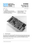
The EV9810 EvKit is available for the evaluation, experimentation and design-in of the CMX981
Advanced Digital Radio Baseband Processor IC. Comprising a digital/analogue pcb with an on-board
CMX981 device, the evkit provides access to the CMX981’s baseband signal, control and data interfaces
as well as its ADC and DAC on-chip functions. Additionally, an onboard codec interface provides
microphone, earphone and loudspeaker inputs and outputs via jack sockets.
Widely populated by jumpers, links and test points this hardware kit allows the user to dynamically
monitor and/or isolate all aspects of the IC’s signal and voltage levels.
This evkit has a simple power requirement with on-board voltage regulation and distribution.
© 2005 CML Microsystems Plc
Evaluation Kit User Manual for CMX981
EV9810
CONTENTS
Section
Page
1
Brief Description ..................................................................................... 1
2.
Preliminary Information.......................................................................... 5
2.1
Laboratory Equipment............................................................... 5
2.2
Handling Precautions ................................................................ 5
2.3
Approvals.................................................................................... 5
3.
Signal Lists .............................................................................................. 6
5.
Detailed Description ............................................................................. 11
5.1
Hardware Description.............................................................. 11
5.2
Adjustments and Controls ...................................................... 11
5.3
Troubleshooting....................................................................... 12
6.
Performance Specification................................................................... 13
6.1
Electrical Performance ............................................................ 13
© 2005 CML Microsystems Plc
2
UM/9810/2
Evaluation Kit User Manual for CMX981
EV9810
Figure 1 CMX981 Block Diagram
© 2005 CML Microsystems Plc
3
UM/9810/2
Evaluation Kit User Manual for CMX981
EV9810
Figure 2 EV9810 Block Diagram
© 2005 CML Microsystems Plc
4
UM/9810/2
Evaluation Kit User Manual for CMX981
2.
Preliminary Information
2.1
Laboratory Equipment
EV9810
The following laboratory equipment is needed to use this evaluation kit:
2.1.1
Dual Power Supply
±8V (nominal), 500mA
2.2
Handling Precautions
Like most evaluation kits, this product is designed for use in office and laboratory environments.
The following practices will help ensure its proper operation.
2.2.1
Static Protection
This product uses low power CMOS circuits which can be damaged by electrostatic discharge.
Partially damaged circuits can function erroneously, leading to misleading results. Observe ESD
precautions at all times when handling this product.
2.2.2
Contents - Unpacking
Please ensure that you have received all of the items on the separate information sheet (EV9810)
and notify CML within 7 working days if the delivery is incomplete.
2.3
Approvals
There are no approvals for this product.
© 2005 CML Microsystems Plc
5
UM/9810/2
Evaluation Kit User Manual for CMX981
3.
EV9810
Signal Lists
CONNECTOR PINOUT
Connector
Ref.
Connector
Pin No.
Signal
Name
Signal
Type
J2
1
IRXPL
O/P
I channel receive, positive ouput from opamp
2
IRXP
I/P
I channel receive, positive input to
CMX981
3
IRXNL
O/P
I channel receive, negative ouput from opamp
4
IRXN
I/P
I channel receive, negative input to
CMX981
J2
5, 6
AGND
Power
J2
7
QRXNL
O/P
Q channel receive, negative ouput from
op-amp
8
QRXN
I/P
Q channel receive, negative input to
CMX981
9
QRXPL
O/P
Q channel receive, positive ouput from opamp
10
QRXP
I/P
Q channel receive, positive input to
CMX981
J5
1
AUXADC2
I/P
Auxiliary ADC 2 output
J5
3
AUXADC1
I/P
Auxiliary ADC 1 output
J5
5
AUXADC3
I/P
Auxiliary ADC 3 output
J5
7
AUXADC4
I/P
Auxiliary ADC 4 output
J5
9
AUXADC5
I/P
Auxiliary ADC 5 output
J5
11
AUXADC6
I/P
Auxiliary ADC 6 output
J5
13
AUXDAC2
O/P
Auxiliary DAC 2 input
J5
15
AUXDAC1
O/P
Auxiliary DAC 1 input
J5
17
AUXDAC3
O/P
Auxiliary DAC 3 input
J5
19
AUXDAC4
O/P
Auxiliary DAC 4 input
J5
2, 4, 6, 8,
10, 12, 14,
16, 18, 20
AGND
Power
J2
J2
J2
J2
J2
J2
© 2005 CML Microsystems Plc
6
Description
Analogue ground
Analogue ground
UM/9810/2
Evaluation Kit User Manual for CMX981
EV9810
CONNECTOR PINOUT
Connector
Ref.
Connector
Pin No.
Signal
Name
Signal
Type
J6
1
AUDPN
O/P
Audio power amp, negative output.
J6
2
AUDPP
O/P
Audio power amp, positive output.
J7
1, 29
VEXT
Power
Host power rail for level shifters
J7
3
N_IRQ2
O/P
CMX981 – Interrupt Request 2
J7
5
SCMDRDFS2
O/P
CMX981 – FSB2 Read Frame Sync
J7
7
SCMDFS2
I/P
CMX981 – FSB2 Frame Sync
J7
9
SCMDRDDATA2
O/P
CMX981 – FSB2 Read Data
J7
11
SCMDDATA2
I/P
CMX981 – FSB2 Data
J7
13
SCLK
O/P
CMX981- Serial Clock
J7
15
N_RESET
I/P
CMX981 – Reset Pin
J7
17
SRXFS
O/P
CMX981 – FSB3, Receive Frame Sync
J7
19
SRXDATA
O/P
CMX981 – FSB3, Receive Data
J7
21
STXFS
I/P
CMX981 – FSB3 Transmit Frame Sync
J7
23
STXDATA
I/P
CMX981 – FSB3, Transmit Data
J7
25
N_IRQ1
O/P
CMX981 – Interrupt Request 1
J7
27
SYMCLK
O/P
CMX981 – symbol clock output
J7
31
CSN
I/P
CMX981 – C-BUS chip select,
Description
FSB1 Read Frame Sync
J7
33
CCLK
I/P
CMX981 – C-BUS clock,
FSB1 Frame Sync
J7
35
RDATA
O/P
CMX981 – C-BUS read data,
FSB1 Read Data
J7
37
CDATA
I/P
CMX981 – C-BUS data,
FSB1 Data
J7
39
© 2005 CML Microsystems Plc
CBUSEN
I/P
7
CMX981 C-BUS/FSB1 select.
UM/9810/2
Evaluation Kit User Manual for CMX981
EV9810
CONNECTOR PINOUT
Connector
Ref.
Connector
Pin No.
Signal
Name
Signal
Type
J7
2, 4, 6, 8,
10, 12,14,
16, 18, 20,
22, 24, 26,
28, 30, 32,
34, 36, 38,
40
DGND
Power
J9
J9
1
ITXPL
I/P
I channel transmit, positive input to op-amp
2
ITXP
O/P
I channel transmit, positive output from
CMX981
3
ITXNL
I/P
I channel transmit, negative input to opamp
4
ITXN
O/P
I channel transmit, negative output from
CMX981
J9
5, 6
AGND
Power
J9
7
QTXNL
I/P
Q channel transmit, negative input to opamp
8
QTXN
O/P
Q channel transmit, negative output from
CMX981
9
QTXPL
I/P
Q channel transmit, positive input to opamp
10
QTXP
O/P
CMX981 - Q channel transmit, positive
output from CMX981
J10
TIP
MIC1P
I/P
CMX981 – MIC1, positive input
J10
RING
MIC1N
I/P
CMX981 – MIC1, negative input
J10
SLEEVE
NC
J11
TIP
MIC2P
I/P
CMX981 – MIC2, positive input
J11
RING
MIC2N
I/P
CMX981 – MIC2, negative input
J12
TIP
EAR
O/P
CMX981 – Earpiec output
J12
RING
AGND
Power
J17
1
QTX
O/P
J9
J9
J9
J9
J9
© 2005 CML Microsystems Plc
8
Description
Digital ground
Analogue ground
Analogue ground
Q channel Tx, single ended output
UM/9810/2
Evaluation Kit User Manual for CMX981
EV9810
CONNECTOR PINOUT
Connector
Ref.
Connector
Pin No.
Signal
Name
Signal
Type
J18
1
ITx
O/P
I channel Tx, single ended output
J24
1
IRX
I/P
I channel Rx, single ended input
J25
1
QRX
I/P
Q channel Rx, single ended input
J29
J29
1
+V
2
AGND
Power
Power
J29
3
Power
-V
Description
EV9810 power supply
EV9810 power supply
EV9810 power supply
TEST POINTS
Test Point
Ref.
Default
Measurement
TP1
+2.5 Volts
TP2, TP3
0 Volts
Digital ground
TP4, TP5
0 Volts
Analogue ground
TP6
+5.0 Volts
+5V0 – Power rail for analogue interface.
TP7
-5.0 Volts
-5V0 – Power rail for analogue interface.
TP8
+3.3 Volts
VDDIO– CMX981 I/O power rail
TP9
+2.5 Volts
VDDD – CMX981 Digital power rail
TP10
+2.5 Volts
VDDA – CMX981 Analogue power rail
TP13 - 16
0 Volts
CMX981 Auxilliary DAC4-1
TP17 – 20
-
CMX981 Auxilliary ADC4-1
TP25
TP26
Description
VDDPA
CMX981 Auxilliary ADC5
-
CMX981 Auxilliary ADC6
JUMPERS/LINKS
Link
Ref.
Positions
Default
Position
J13
1-2/2-3
2-3
Select power rail for level shifting, 1-2 is host power, 2-3 is
+3V3 rail (VDDIO)
J14
1-2/2-3
2-3
Select power rail for level shifting, 1-2 is host power, 2-3 is
+3V3 rail (VDDIO)
Notes: I/P
O/P
BI
NC
© 2005 CML Microsystems Plc
=
=
=
=
Description
Input
Output
Bidirectional
Not connected
9
UM/9810/2
Evaluation Kit User Manual for CMX981
4.
EV9810
Circuit Schematics and Board Layouts
For clarity circuit schematics are included as separate, high resolution, files in pdf format.
Figure 3 Evaluation Board - Layout
© 2005 CML Microsystems Plc
10
UM/9810/2
Evaluation Kit User Manual for CMX981
5.
Detailed Description
5.1
Hardware Description
EV9810
The serial interface ports for the CMX981 are brought out to a 40 pin header, J7. All signals are
buffered and can be level shifted, to nominally 5 volt logic, by the following procedure:
• Connect J7 pins 1 and 29 to power rail of external logic.
• Position jumpers, J13 and J14 to short circuit pins 1 and 2, leaving pins 2 and 3 open
circuit. This position is marked as ‘Ext’ on the pcb silk screen.
The board can be powered by a standard bench dual power supply unit. All the power rail levels
required by the EV9810 circuitry are generated with on board regulators. Note that the +5 volt and
–5 volt rails are provided for the baseband interface only and are not required by the CMX981
itself.
The Baseband interface provides conversion to and from the differential I and Q channel signals
of the CMX981 from and to single ended signals. The single ended signals are brought to SMA
sockets. This circuitry may be isolated, and the differential signals accessed, by removing
jumpers across the following points:
Signal
IRXP
IRXN
QRXN
QRXP
ITXP
ITXN
QTXN
QTXP
Jumper Position
J2 pin 1 to J2 pin 2
J2 pin 3 to J2 pin 4
J2 pin 9 to J2 pin 10
J2 pin 7 to J2 pin 8
J9 pin 1 to J9 pin 2
J9 pin 3 to J9 pin 4
J9 pin 7 to J9 pin 8
J9 pin 9 to J9 pin 10
For the microphone inputs and the earpiece output the CMX981 codec audio connections are
brought out to 3.5mm mono jacks. The audio power amplifier outputs are brought to a terminal
block, J6, across which an 8Ω speaker may be connected.
The CMX981 auxilliary DAC outputs and ADC inputs are brought to both a pin header, J5, and
individual test points.
An on-board oscillator circuit provides the 9.216MHz for MCLK of the CMX981.
Separate digital and analogue ground planes are provided. These are connected via 0R link, R3,
which is on the underside of the PCB.
5.2
Adjustments and Controls
None.
© 2005 CML Microsystems Plc
11
UM/9810/2
Evaluation Kit User Manual for CMX981
5.3
EV9810
Troubleshooting
•
The +5 volt supply, measured at TP6, is not at 5 volts:
Ensure that + and – 8 volts supplies are applied at the same time.
•
Achieving the best performance from the receive path A to D converters:
To get the lowest noise levels at the RxI and RxQ inputs, the user should ensure that their
test signal source is correctly terminated. This could be achieved by attaching a T-piece to
the appropriate input connector. One side of the T-piece is fed from the signal source whilst
the other side is used to terminate the cable.
© 2005 CML Microsystems Plc
12
UM/9810/2
Evaluation Kit User Manual for CMX981
EV9810
6.
Performance Specification
6.1
Electrical Performance
6.1.1
Absolute Maximum Ratings
Exceeding these maximum ratings can result in damage to the Evaluation Kit.
Supply
+V
-V
Voltage on any connector J7 pin to VSS ,
Voltage on any other pin
Current into or out of any +V or -V and Vss pins
Storage Temperature
Operating Temperature
Min.
Max.
Units
-0.3
+0.3
-0.3
-0.3
0
-10
+10
12.0
-12.0
VDDIO + 0.3
VDDD + 0.3
+/-150
+70
+35
V
V
V
mA
°C
°C
Min.
Max.
Units
7.5
-7.5
+10
8.5
-8.5
+35
V
V
°C
6.1.2 Operating Limits
Correct operation of the Evaluation Kit outside these limits is not implied.
Notes
Supply
(+V – Vss)
(-V – Vss)
Operating Temperature
6.1.3
Operating Characteristics
For the following conditions unless otherwise specified:
Evaluation Device Xtal Frequency = 9.216MHz.
Notes
DC Parameters
Voltage regulator outputs
+2V5PA (VDDPA)
+2V5A (VDDA)
+2V5D (VDDD)
+3V3
(VDDIO)
+5V0
-5V0
Typ.
Max.
2.5
2.5
2.5
3.3
5.0
-5.0
Supply current
I+V
I-V
Notes: 1.
Min.
1
75
55
Units
V
V
V
V
V
V
230
60
mA
mA
Maximum value occurs when driving Audio PA into 8Ω
© 2005 CML Microsystems Plc
13
UM/9810/2
Evaluation Kit User Manual for CMX981
EV9810
CML does not assume any responsibility for the use of any circuitry described. No IPR or circuit patent licences are implied.
CML reserves the right at any time without notice to change the said circuitry and any part of this product specification.
Evaluation kits and demonstration boards are supplied for the sole purpose of demonstrating the operation of CML products
and are supplied without warranty. They are intended for use in a laboratory environment only and are not for re-sale, enduse or incorporation into other equipments. Operation of these kits and boards outside a laboratory environment is not
permitted within the European Community. All software/firmware is supplied "as is" and is without warranty. It forms part of
the product supplied and is licensed for use only with this product, for the purpose of demonstrating the operation of CML
products. Whilst all reasonable efforts are made to ensure that software/firmware contained in this product is virus free, CML
accepts no resonsibility whatsoever for any contamination which results from using this product and the onus for checking
that the software/firmware is virus free is placed on the purchaser of this evaluation kit or development board.
www.cmlmicro.com
For FAQs see: www.cmlmicro.com/products/faqs/
For a full data sheet listing see: www.cmlmicro.com/products/datasheets/download.htm
For detailed application notes: www.cmlmicro.com/products/applications/
Oval Park, Langford,
Maldon, Essex,
CM9 6WG - England.
4800 Bethania Station Road,
Winston-Salem,
NC 27105 - USA.
No 2 Kallang Pudding Road,
#09 - 05/06 Mactech
Industrial Building,
Singapore 349307
No. 218, Tian Mu Road
West, Tower 1, Unit 1008,
Shanghai Kerry Everbright
City, Zhabei,
Shanghai 200070,
China.
Tel: +44 (0)1621 875500
Tel: +65 6745 0426
Fax: +44 (0)1621 875600
Tel: +1 336 744 5050,
800 638 5577
Fax: +1 336 744 5054
Fax: +65 6745 2917
Tel: +86 21 6317 4107
+86 21 6317 8916
Fax: +86 21 6317 0243
Sales:
[email protected]
Sales:
[email protected]
Sales:
[email protected]
Sales:
[email protected]
Technical Support:
[email protected]
Technical Support:
[email protected]
Technical Support:
[email protected]
Technical Support:
[email protected]