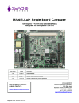
1
FP-GPIO96
FeaturePak™ I/O Module with 96 Digital I/O Points
Rev A.01 November 2013
Revision
Date
A.00
1/17/11
Initial version
A.01
11/14/13
Added pinout information
FOR TECHNICAL SUPPORT
PLEASE CONTACT:
[email protected]
Comment
Copyright 2013
Diamond Systems Corporation
1255 Terra Bella Ave.
Mountain View, CA 94043 USA
Tel 1-650-810-2500
Fax 1-650-810-2525
www.diamondsystems.com
CONTENTS
Important Safe Handling Information .....................................................................................................................3
1. Introduction .......................................................................................................................................................4
1.1 Description .....................................................................................................................................................4
1.2 Features .........................................................................................................................................................4
1.3 FeaturePak Resources ..................................................................................................................................5
2. Functional Overview .........................................................................................................................................6
2.1 Functional Block Diagram ..............................................................................................................................6
2.2 Board Drawing ...............................................................................................................................................7
3. Connector Pinout and Pin Description ...........................................................................................................8
3.1 FeaturePak Connector ..................................................................................................................................8
3.1.1
PCI Express ..........................................................................................................................................8
3.1.2
System Interface Signals ......................................................................................................................8
3.2 FeaturePak Connector Pinout .......................................................................................................................9
3.3 Digital I/O Signals ....................................................................................................................................... 10
3.3.1
Primary I/O connector ........................................................................................................................ 10
3.3.2
Secondary I/O connector ................................................................................................................... 11
4. Theory of Operation....................................................................................................................................... 12
4.1 DIO Blocks .................................................................................................................................................. 12
4.2 Counter/Timer and PWM Block .................................................................................................................. 12
4.3 Interrupts ..................................................................................................................................................... 12
5. Board Configuration ...................................................................................................................................... 13
5.1 Configuring Using Universal Driver ............................................................................................................ 13
5.2 Configuring Using Register Operations ...................................................................................................... 13
5.2.1
Interrupt level ..................................................................................................................................... 13
6. I/O Registers ................................................................................................................................................... 14
6.1 I/O Map Summary....................................................................................................................................... 14
6.2 I/O Register Details .................................................................................................................................... 15
6.2.1
BAR0 + 32 (0x20) DIO Block A Registers ......................................................................................... 16
6.2.2
BAR0 + 32 (0x20) DIO Block B Registers ......................................................................................... 20
6.2.3
BAR0 + 48 (0x30) Counters, PWM Block Registers.......................................................................... 23
6.2.4
BAR0 + 112 (0x70) Interrupts, Miscellaneous, and ID Block Registers ........................................... 29
6.2.5
BAR0 + 224 (0xE0) SPI Flash Interface Block Registers ................................................................. 34
7. Digital I/O Operation ...................................................................................................................................... 37
7.1 Digital I/O Configuration Register ............................................................................................................... 38
7.2 Outputting data to a DIO port ..................................................................................................................... 38
7.3 Reading data from a DIO port .................................................................................................................... 39
8. Counter/Timer Operation .............................................................................................................................. 39
8.1 Counter/Timer Features and Configuration Options .................................................................................. 39
8.2 Counter/Timer Configuration ...................................................................................................................... 40
8.3 Counter/Timer Access and Programming .................................................................................................. 40
8.3.1
Counter/Timer commands ................................................................................................................. 41
8.4 Timer interrupts........................................................................................................................................... 44
9. PWM Operation .............................................................................................................................................. 45
10. Specifications................................................................................................................................................. 46
FP-GPIO96 User Manual Rev A.01
www.diamondsystems.com
Page 2
IMPORTANT SAFE HANDLING INFORMATION
WARNING!
ESD-Sensitive Electronic Equipment
Observe ESD-safe handling procedures when working with this product.
Always use this product in a properly grounded work area and wear appropriate
ESD-preventive clothing and/or accessories.
Always store this product in ESD-protective packaging when not in use.
Safe Handling Precautions
The FP-GPIO96 board contains a high density connector with many connections to sensitive electronic
components. This creates many opportunities for accidental damage during handling, installation and connection
to other equipment. The list here describes common causes of failure found on boards returned to Diamond
Systems for repair. This information is provided as a source of advice to help you prevent damaging your
Diamond (or any vendor’s) embedded computer boards.
ESD damage – This type of damage is usually almost impossible to detect, because there is no visual sign of
failure or damage. The symptom is that the board eventually simply stops working, because some component
becomes defective. Usually the failure can be identified and the chip can be replaced. To prevent ESD damage,
always follow proper ESD-prevention practices when handling computer boards.
Damage during handling or storage – On some boards we have noticed physical damage from mishandling. A
common observation is that a screwdriver slipped while installing the board, causing a gouge in the PCB surface
and cutting signal traces or damaging components.
Another common observation is damaged board corners, indicating the board was dropped. This may or may not
cause damage to the circuitry, depending on what is near the corner. Most of our boards are designed with at
least 25 mils clearance between the board edge and any component pad, and ground / power planes are at least
20 mils from the edge to avoid possible shorting from this type of damage. However these design rules are not
sufficient to prevent damage in all situations.
A third cause of failure is when a metal screwdriver tip slips, or a screw drops onto the board while it is powered
on, causing a short between a power pin and a signal pin on a component. This can cause overvoltage / power
supply problems described below. To avoid this type of failure, only perform assembly operations when the
system is powered off.
Sometimes boards are stored in racks with slots that grip the edge of the board. This is a common practice for
board manufacturers. However our boards are generally very dense, and if the board has components very close
to the board edge, they can be damaged or even knocked off the board when the board tilts back in the rack.
Diamond recommends that all our boards be stored only in individual ESD-safe packaging. If multiple boards are
stored together, they should be contained in bins with dividers between boards. Do not pile boards on top of each
other or cram too many boards into a small location. This can cause damage to connector pins or fragile
components.
Power supply wired backwards – Our power supplies and boards are not designed to withstand a reverse
power supply connection. This will destroy each IC that is connected to the power supply (i.e. almost all ICs). In
this case the board will most likely will be unrepairable and must be replaced. A chip destroyed by reverse power
or by excessive power will often have a visible hole on the top or show some deformation on the top surface due
to vaporization inside the package. Check twice before applying power!
Overvoltage on digital I/O line – If a digital I/O signal is connected to a voltage above the maximum specified
voltage, the digital circuitry can be damaged. On most of our boards the acceptable range of voltages connected
to digital I/O signals is 0-5V, and they can withstand about 0.5V beyond that (-0.5 to 5.5V) before being damaged.
However logic signals at 12V and even 24V are common, and if one of these is connected to a 5V logic chip, the
chip will be damaged, and the damage could even extend past that chip to others in the circuit
FP-GPIO96 User Manual Rev A.01
www.diamondsystems.com
Page 3
1. INTRODUCTION
1.1
Description
TM
FP-GPIO96 is a general purpose I/O FeaturePak module using a high-capacity (700K gate equivalent) PCI
Express FPGA for maximum density and flexibility. The base hardware configuration features 96 digital I/O lines
grouped into 12 8-bit ports. All ports have I/O buffers to protect the FPGA and offers 3.3V logic drive levels. The
ports are organized into a combination of byte-wide, nibble-wide, and bit-wide direction control for maximum
flexibility and application compatibility.
The built-in FPGA personality provides multiple configuration options. All 96 I/O lines may be used in common I/O
mode. Six of these ports can be reconfigured to enable an array of additional features, including 8 32-bit up/down
counter/timers with programmable input source and gate, 4 24-bit PWM circuits with 0-100% duty cycle capability,
and interrupt/latched mode operation.
1.2
Features
Digital I/O
96 total I/O lines brought out to the FeaturePak connector
o
48 I/O lines on the primary I/O connector with 3 8-bit buffers and 2 4-bit buffers for increased
direction configuration flexibility
o
48 I/O lines on the secondary I/O connector with 6 8-bit buffers
Configurable digital I/O pull-up/down resistors, each I/O group independently configurable
Byte-wide, nibble-wide and bit-wide port direction control
Counter/Timers and Triggering
8 32-bit counter/timers for timing and general purpose use
4 24-bit pulse-width modulator circuits
Miscellaneous
One PCI Express x1 lane host interface
+3.3VDC input voltage
FeaturePak form-factor compliant
Zero height expansion module
-40°C to +85°C operating temperature
Universal Driver software support
FP-GPIO96 User Manual Rev A.01
www.diamondsystems.com
Page 4
1.3
FeaturePak Resources
The following table identifies which resources among those defined by the FeaturePak specification that are used
in this product:
FP-GPIO96 User Manual Rev A.01
www.diamondsystems.com
Page 5
2. FUNCTIONAL OVERVIEW
2.1
Functional Block Diagram
FP-GPIO96 User Manual Rev A.01
www.diamondsystems.com
Page 6
2.2
Board Drawing
FP-GPIO96 User Manual Rev A.01
www.diamondsystems.com
Page 7
3. CONNECTOR PINOUT AND PIN DESCRIPTION
3.1
FeaturePak Connector
The FP-GPIO96 uses the FeaturePak standard, which provides a card form-factor and connector suitable for
high-density, compact applications. See http://featurepak.org/ for further details of the FeaturePak embedded I/O
modules standard, including the specification.
In this document we will use the terms FeaturePak edge card connector and MXM connector interchangeably.
The FP-GPIO96 uses an MXM 230-pin connector for all I/O, both to the main computer and for user I/O
connections. The board contains gold-plated fingers conforming to the MXM physical standard for interfacing to
the MXM connector.
The system interface signals on the MXM connector are predefined for all FeaturePak modules and a portion of
pins are reserved for individual module I/O and are freely assignable for each module. Signals are grouped into
several categories:
System interface (PCIe)
Slot/card management signals
Dedicated user I/O
Power/ground
Reserved for future expansion
The module connects to five reserved pins to provide compatibility with possible future expansion of the
FeaturePak standard.
The user I/O consists of 100 signals organized as 2 50-pin groups. On a general purpose baseboard, these
signals directly drive 2 50-pin I/O connectors. The 50-pin connectors may then be connected to applicationspecific cabling, or an I/O adapter board may be plugged onto them to provide a custom I/O connector
configuration for the system enclosure. A custom or application-specific main board may elect to use these
signals in any way desired without conflicting with the standard.
A special feature of the FeaturePak I/O pin assignment is the electrical isolation provided on 32 of the module I/O
pins on the primary 50-pin connector. These pins are separated from each other and from other connector pins by
34 unassigned pins (marked NC) which are to be left unconnected on the main board (no pads or traces leading
to these pins). The module omits the corresponding fingers on the edge connector.
3.1.1
PCI Express
The FP-GPIO96 uses a single PCI Express x1 link for its host interface and does not use the USB or serial
interfaces allowed in the FeaturePak specification. It is reset by the PCI-Reset- input signal. The module routes
the Slot ID signals to a register for readback by the host, and it drives the Present- output line low.
3.1.2
System Interface Signals
Not all functionalities that are defined in the FeaturePak socket standard are supported by the FP-GPIO96
module. For example, the USB, SMBus and serial port interfaces are not utilized on this card.
FP-GPIO96 User Manual Rev A.01
www.diamondsystems.com
Page 8
3.2
FeaturePak Connector Pinout
This section indicates standard FeaturePak connector signal assignments. The I/OA and I/OB pin groups are mapped to
specific I/O functions implemented by the FP-GPIO96 board, as indicated in following sections.
Pins 1 – 114
+3.3V
+3.3V
Ground
PCIe-TX1+
PCIe-TX1Ground
PCIe-CLK1+
PCIe-CLK1Ground
PCIe-TX2+
PCIe-TX2Ground
PCIe-ResetReserved
Reserved
Reserved
Reserved
Ground
USB-Ch1+
USB-Ch1Ground
+3.3V
+3.3V
Serial-TX1
Serial-RTS1
SMBalert#
Slot ID 2
Slot ID 0
JTAG-TDI
JTAG-CLK
Sys-Reset+3.3V
+3.3V
Reserved
Reserved
+3.3V
Reserved
Reserved
+3.3V
Reserved
Reserved
Reserved
Reserved
+5V
+5V
(Ground) I/OB-50
I/OB-48
I/OB-46
I/OB-44
I/OB-42
I/OB-40
I/OB-38
I/OB-36
I/OB-34
I/OB-32
I/OB-30
I/OB-28
1
3
5
7
9
11
13
15
17
19
21
23
25
27
29
31
33
35
37
39
41
43
45
47
49
51
53
55
57
59
61
63
65
67
69
71
73
75
77
79
81
83
85
87
89
91
93
95
97
99
101
103
105
107
109
111
113
2
4
6
8
10
12
14
16
18
20
22
24
26
28
30
32
34
36
38
40
42
44
46
48
50
52
54
56
58
60
62
64
66
68
70
72
74
76
78
80
82
84
86
88
90
92
94
96
98
100
102
104
106
108
110
112
114
FP-GPIO96 User Manual Rev A.01
Pin 115 – 230
+12V
PS-Current
Ground
PCIe-RX1+
PCIe-RX1Ground
PCIe-CLK2+
PCIe-CLK2Ground
PCIe-RX2+
PCIe-RX2Ground
Reserved
Reserved
Reserved
Reserved
Reserved
Ground
USB-Ch2+
USB-Ch2Ground
USB-OC1/2Serial-RX1
Serial-CTS1
SMBclk
SMBdata
Slot ID 1
PresentJTAG-TDO
JTAG-TMS
Reserved
Ground
Ground
Reserved
Reserved
Ground
Reserved
Reserved
Ground
Reserved
Reserved
Reserved
Reserved
Ground
Ground
I/OB-49 (+3.3V)
I/OB-47
I/OB-45
I/OB-43
I/OB-41
I/OB-39
I/OB-37
I/OB-35
I/OB-33
I/OB-31
I/OB-29
I/OB-27
I/OB-26
I/OB-24
I/OB-22
I/OB-20
I/OB-18
I/OB-16
I/OB-14
I/OB-12
I/OB-10
I/OB-8
I/OB-6
I/OB-4
I/OB-2
+5V
+5V
+5V
(Ground) I/OA-50
I/OA-48
I/OA-46
I/OA-44
I/OA-42
I/OA-40
I/OA-38
I/OA-36
(NC)
I/OA-34
(NC)
I/OA-32
(NC)
I/OA-30
(NC)
I/OA-28
(NC)
I/OA-26
(NC)
I/OA-24
(NC)
I/OA-22
(NC)
I/OA-20
(NC)
I/OA-18
(NC)
I/OA-16
(NC)
I/OA-14
(NC)
I/OA-12
(NC)
I/OA-10
(NC)
I/OA-8
(NC)
I/OA-6
(NC)
I/OA-4
(NC)
I/OA-2
www.diamondsystems.com
115
117
119
121
123
125
127
129
131
133
135
137
139
141
143
145
147
149
151
153
155
157
159
161
163
165
167
169
171
173
175
177
179
181
183
185
187
189
191
193
195
197
199
201
203
205
207
209
211
213
215
217
219
221
223
225
227
229
116
118
120
122
124
126
128
130
132
134
136
138
140
142
144
146
148
150
152
154
156
158
160
162
164
166
168
170
172
174
176
178
180
182
184
186
188
190
192
194
196
198
200
202
204
206
208
210
212
214
216
218
220
222
224
226
228
230
I/OB-25
I/OB-23
I/OB-21
I/OB-19
I/OB-17
I/OB-15
I/OB-13
I/OB-11
I/OB-9
I/OB-7
I/OB-5
I/OB-3
I/OB-1
Ground
Ground
Ground
I/OA-49 (+3.3V)
I/OA-47
I/OA-45
I/OA-43
I/OA-41
I/OA-39
I/OA-37
I/OA-35
(NC)
I/OA-33
(NC)
I/OA-31
(NC)
I/OA-29
(NC)
I/OA-27
(NC)
I/OA-25
(NC)
I/OA-23
(NC)
I/OA-21
(NC)
I/OA-19
(NC)
I/OA-17
(NC)
I/OA-15
(NC)
I/OA-13
(NC)
I/OA-11
(NC)
I/OA-9
(NC)
I/OA-7
(NC)
I/OA-5
(NC)
I/OA-3
(NC)
I/OA-1
Page 9
3.3
Digital I/O Signals
3.3.1
Primary I/O connector
The signals on this connector have multiple definitions. The power-up definition is 6 8-bit digital I/O ports
configured as inputs. Up to 8 counter/timers, 4 pulse-width modulators, 1 watchdog timer, and 1 external interrupt
source can also be independently enabled on selected I/O pins as shown in the diagram below. Counters are
enabled in groups of 4. When counter group 1 is enabled, counters 0-3 inputs appear on port A, which is
configured as input, and the outputs appear on Port C 0-3, which is configured as output. When counter group 2
is enabled, counters 4-7 inputs appear on port B, which is configured as input, and the outputs appear on Port C
4-7, which is configured as output. The signals on this port have programmable pull-up/down resistors. All signals
are pulled in the same direction using a control register bit. Each connector group may have independently
configured pull-up/down.
FeaturePak pin no.
230
226
222
218
214
210
206
202
198
194
190
186
182
178
174
170
166
162
160
158
156
154
152
150
148
I/O pin no.
Ctr 0 In / DIO A0
Ctr 1 In / DIO A2
Ctr 2 In / DIO A4
Ctr 3 In / DIO A6
Ctr 4 In / DIO B0
Ctr 5 In / DIO B2
Ctr 6 In / DIO B4
Ctr 7 In / DIO B6
Ctr 0 Out / DIO C0
Ctr 2 Out / DIO C2
Ctr 4 Out / DIO C4
Ctr 6 Out / DIO C6
DIO D0
DIO D2
DIO D4
DIO D6
DIO E0
DIO E2
DIO E4
DIO E6
PWM 0 / DIO F0
PWM 2 / DIO F2
WDT In / DIO F4
DIO F6
+3.3V
Signal Name
DIO A7-A0
DIO B7-B0
DIO C7-C0
DIO D7-D0
DIO E7-E0
DIO F7-F0
In 1-10
Gate 1-10
Out 1-10
PWM3-0
WDTOUT, WDTIN
Interrupt
+3.3V
Ground
FP-GPIO96 User Manual Rev A.01
1
3
5
7
9
11
13
15
17
19
21
23
25
27
29
31
33
35
37
39
41
43
45
47
49
2
4
6
8
10
12
14
16
18
20
22
24
26
28
30
32
34
36
38
40
42
44
46
48
50
FeaturePak pin no.
DIO A1 / Ctr 0 Gate
DIO A3 / Ctr 1 Gate
DIO A5 / Ctr 2 Gate
DIO A7 / Ctr 3 Gate
DIO B1 / Ctr 4 Gate
DIO B3 / Ctr 5 Gate
DIO B5 / Ctr 6 Gate
DIO B7 / Ctr 7 Gate
DIO C1 / Ctr 1 Out
DIO C3 / Ctr 3 Out
DIO C5 / Ctr 5 Out
DIO C7 / Ctr 7 Out
DIO D1
DIO D3
DIO D5
DIO D7
DIO E1
DIO E3
DIO E5
DIO E7
DIO F1 / PWM 1
DIO F3 / PWM 3
DIO F5 / WDT Out
DIO F7 / Interrupt In
Ground
229
225
221
217
213
209
205
201
197
193
189
185
181
177
173
169
165
161
159
157
155
153
151
149
147
Definition
Digital I/O port A
Digital I/O port B
Digital I/O port C; also functions as counter/timers 0-1 and PWM 0-1
Digital I/O port D; also functions as counter/timers 2-3 and PWM 2-3
Digital I/O port E; also functions as counter/timers 4-5 and interrupt input
Digital I/O port F; also functions as counter/timers 6-7 and watchdog timer I/O
Counter input signals
Counter gate signals
Counter output signals
Pulse width modulator outputs
Watchdog timer I/O signals
Interrupt input
3.3V power from system
Digital ground
www.diamondsystems.com
Page 10
3.3.2
Secondary I/O connector
The signals on this connector have a single definition: 6 8-bit digital I/O ports with each port’s direction
independently programmable. All ports power up in input mode and all output registers power up to 0. The signals
on this port have programmable pull-up/down resistors. All signals are pulled in the same direction using a control
register bit. Each connector group may have independently configured pull-up/down.
FeaturePak pin no.
140
138
136
134
132
130
128
126
124
122
120
118
116
114
112
110
108
106
104
102
100
98
96
94
92
Signal Name
DIO G7-G0
DIO H7-H0
DIO J7-J0
DIO K7-K0
DIO L7-L0
DIO M7-M0
+3.3V
Ground
FP-GPIO96 User Manual Rev A.01
I/O pin no.
DIO G0
DIO G2
DIO G4
DIO G6
DIO H0
DIO H2
DIO H4
DIO H6
DIO J0
DIO J2
DIO J4
DIO J6
DIO K0
DIO K2
DIO K4
DIO K6
DIO L0
DIO L2
DIO L4
DIO L6
DIO M0
DIO M2
DIO M4
DIO M6
+3.3V
1
3
5
7
9
11
13
15
17
19
21
23
25
27
29
31
33
35
37
39
41
43
45
47
49
2
4
6
8
10
12
14
16
18
20
22
24
26
28
30
32
34
36
38
40
42
44
46
48
50
FeaturePak pin no.
DIO G1
DIO G3
DIO G5
DIO G7
DIO H1
DIO H3
DIO H5
DIO H7
DIO J1
DIO J3
DIO J5
DIO J7
DIO K1
DIO K3
DIO K5
DIO K7
DIO L1
DIO L3
DIO L5
DIO L7
DIO M1
DIO M3
DIO M5
DIO M7
Ground
139
137
135
133
131
129
127
125
123
121
119
117
115
113
111
109
107
105
103
101
99
97
95
93
91
Definition
Digital I/O port G; byte direction programmable, buffered
Digital I/O port H; byte direction programmable, buffered
Digital I/O port J; byte direction programmable, buffered
Digital I/O port K; byte direction programmable, buffered
Digital I/O port L; byte direction programmable, buffered
Digital I/O port M; byte direction programmable, buffered
3.3V power from system
Digital ground
www.diamondsystems.com
Page 11
4. THEORY OF OPERATION
This chapter provides an orientation to the functional architecture of blocks on the board. Additional details are in
the register programming section and specific chapters on various blocks.
4.1
DIO Blocks
The FP-GPIO96 has twelve 8-bit bidirectional digital I/O ports, named A-F and G-M. The DIO blocks are
controlled and configured using registers at BAR0+32 to 47 for ports A-F and BAR0+96 to 111 for ports G-M.
Ports A, B, D, and G-M are 8-bit ports with direction programmable byte by byte. Register bits DIR[A,B,D,G-M]
control the direction of these ports and also the direction of the port pins where a value of 0 = input and 1 =
output. In output mode, the values in these registers drive their associated I/O pins. The logic levels on the I/O
pins may be read back in both input and output modes. These ports reset to 0 and input mode during power-up,
reset, FPGARST=1, or BRDRST=1. If a port is in input mode, its output register may still be written to. When the
port is switched to output mode, the value of the output register will drive the corresponding I/O pins.
Port C is divided into two 4-bit nibbles with independent direction control. DIRCH controls the direction of DIOC74, and DIRCL controls the direction of DIOC3-0.
Ports E-F are 8-bit ports with direction programmable bit by bit according to register bits DIRE7-0 and DIRF7-0
where a value of 0 = input, 1 = output. I/O pins DIOF3-0 may be reassigned as PWM outputs; see the PWM block
description.
Ports A, B, C, and F may be reassigned as counter/timer, PWM, and watchdog timer I/O pins; see the following
sections.
4.2
Counter/Timer and PWM Block
The FP-GPIO96 contains 8 32-bit up/down counter timers and 4 PWM generators.
The counter timers have programmable functions that are controlled and configured using registers at BAR0+48
to 55. The counter timers can be used to generate interrupts on the PCI Express bus. For details see sections on
Interrupt registers and Chapter 7.2.The counters are programmed using a command register at address 5 in the
counter block, a counter number register at address 4, and a 32-bit data register CTRD31-0 at addresses 0-3.
There are four independent 24-bit PWM generators that are controlled and configured using registers at BAR0+56
to 59. The PWM generators are programmed using a register at address 11 for command and PWM number and
a 24-bit data register PWMD23-0 at addresses 8-10.
4.3
Interrupts
Interrupts to the PCI Express Bus can be generated by any of these blocks: DIO, or the counter timers 0-3.
Register control is provided for enabling/disabling interrupts by using registers at BAR0+112 and 113.
FP-GPIO96 User Manual Rev A.01
www.diamondsystems.com
Page 12
5. BOARD CONFIGURATION
The jumperless FP-GPIO96 FeaturePak module is configured by software. The board must first be initialized,
then configured. These operations can be done either using Diamond's Universal Driver (version 7.0 or higher) or
by an independent set of equivalent register operations.
5.1
Configuring Using Universal Driver
Diamond Systems provides a device driver which will enable access to the board functionalities via an easy to
use API set. This driver is called the Universal Driver and is available in Windows XP and Linux 2.6.xx operating
systems. The details on the Universal driver can be found in the Universal Driver manual and can be accessed
online at http://docs.diamondsystems.com/dscud/manual_Main+Page.html. The Universal Driver software comes
on the Diamond Resource CD shipped with this product, or may be downloaded from the FP-GPIO96 webpage at
www.diamondsystems.com/products/fpgpio96.
5.2
Configuring Using Register Operations
The board can also be controlled using simple register read/write commands if you are willing to write your own
driver. In typical modern operating systems, the user level applications cannot directly access the low level
system information and don’t have register level access. In order to communicate with any PCI device, a device
driver is required.
The Universal Driver mentioned above can be also be used to do register-level control, and a programmer could
develop his own driver functionality that uses simple register read/write command after performing a PCI scan
using the Universal Driver. Users of this type of access need to understand the board register map which is
defined in later sections of this manual. This type of approach is suitable for someone who is very aware of the
nature of low-level operations of hardware.
5.2.1
Interrupt level
Interrupts are used for hardware I/O operations that are independent of normal program flow. The FP-GPIO96
can be set up to generate interrupts under several circumstances. The board can generate interrupts to transfer
digital data into the board, as well as at regular intervals according to a programmable timer on the board.
Individual control bits are used to enable each type of interrupt.
Since the FP-GPIO96 board works on PCI Express bus architecture, the interrupt level is obtained as a result of a
PCI scan performed by the device driver. To obtain the interrupt level used by the board, DSC provides a default
device driver which can perform low level PCI commands and provide user level access to the board. The driver
is from a third-party driver developer and is called WinDriver.
If you do not wish to use this driver and would like to develop your own driver, you need to be knowledgeable on
the PCI / PCI express system architecture as well as the device driver model and architecture details for your
chosen operating system.
FP-GPIO96 User Manual Rev A.01
www.diamondsystems.com
Page 13
6. I/O REGISTERS
The FP-GPIO96 register map consists of 256 bytes, divided into 16 16-byte blocks in the system I/O address
space. Direct register access is not required if you are using Diamond's Universal Driver software that ships with
the board. The driver handles all board access and provides a high-level set of functions to simplify programming.
The information presented here and in the next chapter is intended to provide a detailed description of the board’s
features and operation, as well as for programmers who are not using the Universal Driver software.
6.1
I/O Map Summary
Block
(Dec)
Range
(Dec)
Range
(Hex)
0
0-15
0-F
1
16-31
10-1F
2
32-47
20-2F
3
48-63
30-3F
4
64-79
40-4F
5
80-95
50-5F
6
96-111
60-6F
7
112-127
70-7F
8
128-143
80-8F
9
144-159
90-9F
10
160-175
A0-AF
11
176-191
B0-BF
12
192-207
C0-CF
13
208-223
D0-DF
14
224-239
E0-EF
15
240-255
F0-FF
Function
DIO group A
Counters, PWM
DIO group B
Interrupts, Misc., and ID
SPI Flash Interface
The FP-GPIO96 board is a PCI Express based design and has 255 bytes of addressable registers as shown in
the table above. Since in PCI architecture, the I/O base address is obtained as a result of a PCI scan on the
Vendor ID and Device ID of the PCI device, the base address is not shown in the table; instead, offsets from the
base address BAR0 are shown for individual functional blocks.
The FP-GPIO96 Vendor ID is 0x1C0E and the Device ID is 0x0900. When a PCI scan is performed using these
two IDs, the board is detected and the register BAR0 gets the base address for the start of where registers are
mapped. For the user application, the address information of BAR0 serves as the base address of the board and
the rest of the registers are all accessed as an offset from the BAR0 address.
In the following material, register block addresses are shown in a format as in this example:
BAR0 + 32 (0x20)
Read/Write/Command
A/D Block Registers
Where the address is given as BAR0 + offset amount, with the number in decimal and the hex equivalent in
parentheses. This is followed by the register block group name.
Registers are Read, Read/Write, Write, or Command, where Command registers can be written but cannot be
read from.
FP-GPIO96 User Manual Rev A.01
www.diamondsystems.com
Page 14
6.2
I/O Register Details
This section describes the location and general behavior of specific bits in each I/O map register. In all register
definitions below, any bit without a name is not defined and serves no function.
GROUP A
Offset
0
1
2
3
4
5
6
7
8
9
10
11
12
13
14
15
7
6
5
4
3
2
1
0
DIOA7-0
DIOB7-0
DIOC7-0
DIOD7-0
DIOE7-0
DIOF7-0
DIRCH
DIRA
DIRB
DIRCL
DIRD
DIRE7-0
DIRF7-0
GROUP B
Offset
7
6
5
4
3
0
DIOG7-0
1
DIOH7-0
2
DIOJ7-0
3
DIOK7-0
4
DIOL7-0
5
DIOM7-0
2
1
0
6
7
8
DIRG
9
DIRH
10
DIRJ
11
DIRK
12
DIRL
13
DIRM
14
15
FP-GPIO96 User Manual Rev A.01
www.diamondsystems.com
Page 15
6.2.1
BAR0 + 32 (0x20)
DIO Block A Registers
These registers provide control of digital I/O ports. To use the ports, they must first be configured using Mode and
Dir fields, and then can be read from and written to.
BAR0 + 32
(0x20)
Bit No.
Read/Write
7
6
Digital I/O port A
5
4
Name
3
2
1
0
0
0
0
0
DIOA7-0
Reset value
DIOA7-0
0
0
0
0
This register is used for digital I/O on byte addressable port A. When port A is in output
mode, the output signal lines DIO A7-0 (see Section 3.3) will be set to the values in this
register, and reading this register will read back the programmed value. When port A is in
input mode, this register will read back the logic levels on signal lines DIO A7-0, and writing
to this register will have no effect. The direction of port A is controlled by the bit DIRA in the
DIO control register at BAR0+40.
The DIO port A defaults to input mode on power up and all the register bits reset to 0.
BAR0 + 33
(0x21)
Bit No.
Read/Write
7
6
Digital I/O port B
5
4
Name
3
2
1
0
0
0
0
0
DIOB7-0
Reset value
DIOB7-0
0
0
0
0
This register is used for digital I/O on byte addressable port B. When port B is in output
mode, the output signal lines DIO B7-0 (see Section 3.3) will be set to the values in this
register, and reading this register will read back the programmed value. When port B is in
input mode, this register will read back the logic levels on signal lines DIO B7-0, and writing
to this register will have no effect. The direction of port B is controlled by bit DIRB in the DIO
control register at BAR0+41.
The DIO port B defaults to input mode on power up and all the register bits reset to 0.
BAR0 + 34
(0x22)
Bit No.
Read/Write
7
6
Digital I/O port C
5
4
Name
Reset value
DIOC7-0
3
2
1
0
0
0
0
0
DIOC7-0
0
0
0
0
This register is used for digital I/O on byte addressable port C. When port C is in output
mode, the output signal lines DIO C7-0 (see Section 3.3) will be set to the values in this
register, and reading this register will read back the programmed value. When port C is in
input mode, this register will read back the logic levels on signal lines DIO C7-0, and writing
to this register will have no effect. The direction of port C is controlled by bit DIRCH and
DIRCL in the DIO control register at BAR0+42.
The DIO port C defaults to input mode on power up and all the register bits reset to 0.
FP-GPIO96 User Manual Rev A.01
www.diamondsystems.com
Page 16
BAR0 + 35
(0x23)
Bit No.
Read/Write
7
6
Digital I/O port D
5
4
Name
Reset value
DIOD7-0
BAR0 + 36
3
2
1
0
0
0
0
0
DIOD7-0
0
0
0
0
This register is used for digital I/O on byte addressable port D. When port D is in output
mode, the output signal lines DIO D7-0 (see Section 3.3) will be set to the values in this
register, and reading this register will read back the programmed value. When port D is in
input mode, this register will read back the logic levels on signal lines DIO D7-0, and writing
to this register will have no effect. The direction of port D is controlled by bit DIRD in the DIO
control register at BAR0+43. The DIO port D defaults to input mode on power up and all the
register bits reset to 0.
(0x24)
Bit No.
Read/Write
7
6
Digital I/O port E
5
4
Name
3
2
1
0
0
0
0
0
DIOE7-0
Reset value
DIOE7-0
0
0
0
0
This register is used for digital I/O on bit addressable port E. When port E is in output mode,
the output signal lines DIO E7-0 on (see Section 3.3) will be set to the values in this register,
and reading this register will read back the programmed value. When port E is in input mode,
this register will read back the logic levels on signal lines DIO E7-0, and writing to this register
will have no effect. The direction of port E is controlled by DIRE7-0 bits in the register at
BAR0+44. Each bit in the direction register controls the direction of the corresponding port bit.
The DIO port E defaults to input mode on power up and all the register bits reset to 0.
BAR0 + 37
(0x25)
Bit No.
Read/Write
7
6
Digital I/O port F
5
4
Name
3
2
1
0
0
0
0
0
DIOF7-0
Reset value
DIOF7-0
0
0
0
0
This register is used for digital I/O on bit addressable port F. When port F is in output mode,
the output signal lines DIO F7-0 (see Section 3.3) will be set to the values in this register, and
reading this register will read back the programmed value. When port F is in input mode, this
register will read back the logic levels on signal lines DIO F7-0, and writing to this register will
have no effect. The direction of port F is controlled by DIRF7-0 bits in the register at
BAR0+45. Each bit in the direction register controls the direction of the corresponding port bit.
The DIO port F defaults to input mode on power up and all the register bits reset to 0.
BAR0 + 38
(0x26)
Bit No.
Write
7
6
DIO Port A Configuration
5
4
3
2
1
0
Name
DIRA
Reset value
0
This register is used to configure the direction and mode control of the DIO port A. The DIO port A can be
configured in either input or output direction.
DIRA
Direction control bit for DIO port A.
1 = DIO Port A is configured as an output port.
0 = DIO Port A is configured as an input port. (Default setting)
FP-GPIO96 User Manual Rev A.01
www.diamondsystems.com
Page 17
BAR0 + 38
(0x26)
Bit No.
Read
7
DIO Port A Configuration
6
5
4
3
2
1
0
Name
DIRA
Reset value
0
This register provides a read back of the configuration of DIO port A.
DIRA
Read back of the direction setting of DIO port A.
1 = DIO port A is configured as an output.
0 = DIO port A is configured as an input. (Default setting)
BAR0 + 39
(0x27)
Bit No.
Write
7
6
DIO Port B Configuration
5
4
3
2
1
0
Name
DIRB
Reset value
0
This register is used to configure the direction and mode control of the DIO port B. The DIO port B can be
configured in either input or output direction.
DIRB
Read back of the direction setting of DIO port B.
1 = DIO port B is configured as an output.
0 = DIO Port B is configured as an input port. (Default setting)
BAR0 + 39
(0x28)
Bit No.
Read
7
DIO Port B Configuration
6
5
4
3
2
1
Name
0
DIRB
Reset value
This register provides a read back of the configuration of DIO port B.
DIRB
Read back of the direction setting of DIO port B.
1 = DIO port B is configured as an output.
0 = DIO port B is configured as an input. (Default setting)
BAR0 + 40
(0x29)
Bit No.
Write
7
6
DIO Port C Configuration
1
0
Name
5
4
3
2
DIRCH
DIRCL
Reset value
0
0
This register is used to configure the direction and mode control of the DIO port C. Each half of the DIO port C
can be configured in either input or output direction.
DIRCH
Direction control bit for DIO port C upper 4 bits.
1 = DIO Port C7-4 is configured as an output port.
0 = DIO Port C7-4 is configured as an input port. (Default setting)
DIRCL
Direction control bit for DIO port C lower 4 bits.
1 = DIO Port C3-0 is configured as an output port.
0 = DIO Port C3-0 is configured as an input port. (Default setting)
FP-GPIO96 User Manual Rev A.01
www.diamondsystems.com
Page 18
BAR0 + 40
(0x29)
Bit No.
Read
7
DIO Port C Configuration
1
0
Name
6
5
4
3
2
DIRCH
DIRCL
Reset value
0
0
1
0
This register provides a read back of the configuration of DIO port C.
DIRCH
Direction control bit for DIO port C upper 4 bits.
1 = DIO Port C7-4 is configured as an output port.
0 = DIO Port C7-4 is configured as an input port. (Default setting)
DIRCL
Direction control bit for DIO port C lower 4 bits.
1 = DIO Port C3-0 is configured as an output port.
0 = DIO Port C3-0 is configured as an input port. (Default setting)
BAR0 + 41
(0x2A)
Bit No.
Write
7
6
DIO Port D Configuration
5
4
3
2
Name
DIRD
Reset value
0
This register is used to configure the direction and mode control of the DIO port D. The DIO port D can be
configured in either input or output direction.
DIRD
Direction control bit for DIO port D.
1 = DIO Port D is configured as an output port.
0 = DIO Port D is configured as an input port. (Default setting)
BAR0 + 41
(0x2A)
Bit No.
Read
7
DIO Port D Configuration
6
5
4
3
2
1
0
Name
DIRD
Reset value
0
This register provides a read back of the configuration of DIO port D.
DIRD
Read back of the direction setting of DIO port D.
1 = DIO port D is configured as an output.
0 = DIO port D is configured as an input. (Default setting)
FP-GPIO96 User Manual Rev A.01
www.diamondsystems.com
Page 19
BAR0 + 42
(0x2C)
Bit No.
Read/Write
7
6
DIO Port E Configuration
5
4
Name
3
2
1
0
0
0
0
0
DIRE7-0
Reset value
0
0
0
0
This register controls the direction for DIO port E. Each of the DIO port E bits is controllable individually using
corresponding bit in this register as either input or output.
DIRE7-0
These bits provide direction configuration of the DIO port E. When any bit is 0, the
corresponding DIO port E bit is configured as an input while the port bit acts as an output
when the corresponding bit in this register is set to 1.
The default value of this register is 0 which means that all bits of DIO port E are configured as
inputs. Below are a few examples of various configurations.
DIRE7-0 = 0x0F
DIRE7-0 = 0xC0
BAR0 + 43
(0x2D)
Bit No.
- Port E bits 7, 6, 5 and 4 are input while bits 3, 2, 1 and 0 are output.
- Port E bits 7 and 6 are output and all other bits are inputs.
Read/Write
DIO Port F Configuration
7
6
5
4
0
0
0
0
Name
Reset value
3
2
1
0
0
0
0
0
DIRF7-0
This register controls the direction for DIO port F. Each of the DIO port F bits is controllable individually using
corresponding bit in this register as either input or output.
DIRF7-0
These bits provide direction configuration of the DIO port F. When any bit is 0, the
corresponding DIO port F bit is configured as an input while the port bit acts as an output
when the corresponding bit in this register is set to 1.
The default value of this register is 0 which means that all bits of DIO port F are configured as
inputs.
6.2.2
BAR0 + 32 (0x20)
DIO Block B Registers
These registers provide control of digital I/O ports. To use the ports, they must first be configured using Mode and
Dir fields, and then can be read from and written to.
BAR0 + 96
Bit No.
(0x60)
Read/Write
7
6
Digital I/O port G
5
4
Name
Reset value
DIOG7-0
3
2
1
0
0
0
0
0
DIOG7-0
0
0
0
0
This register is used for digital I/O on byte addressable port G. When port G is in output
mode, the output signal lines DIO G7-0 (see Section 3.3) will be set to the values in this
register, and reading this register will read back the programmed value. When port G is in
input mode, this register will read back the logic levels on signal lines DIO G7-0, and writing
to this register will have no effect. The direction of port G is controlled by the bit DIRG in the
DIO control register at BAR0+104.
The DIO port G defaults to input mode on power up and all the register bits reset to 0.
FP-GPIO96 User Manual Rev A.01
www.diamondsystems.com
Page 20
BAR0 + 97
(0x61)
Bit No.
Read/Write
7
6
Digital I/O port H
5
4
Name
3
2
1
0
0
0
0
0
DIOH7-0
Reset value
DIOH7-0
0
0
0
0
This register is used for digital I/O on byte addressable port H. When port H is in output
mode, the output signal lines DIO H7-0 (see Section 3.3) will be set to the values in this
register, and reading this register will read back the programmed value. When port H is in
input mode, this register will read back the logic levels on signal lines DIO H7-0, and writing
to this register will have no effect. The direction of port H is controlled by bit DIRH in the DIO
control register at BAR0+109.
The DIO port H defaults to input mode on power up and all the register bits reset to 0.
BAR0 + 98
(0x62)
Bit No.
Read/Write
7
6
Digital I/O port J
5
4
Name
3
2
1
0
0
0
0
0
DIOJ7-0
Reset value
DIOJ7-0
0
0
0
0
This register is used for digital I/O on byte addressable port J. When port J is in output mode,
the output signal lines DIO J7-0 (see Sec 3.3) are set to the register’s values, and reading
this register reads back the programmed value. When port J is in input mode, this register
reads back the logic levels on signal lines DIO J7-0, writing to this register does nothing. The
direction of port C is controlled by bit DIRJ in the DIO control register at BAR0+110.
The DIO port J defaults to input mode on power up and all the register bits reset to 0.
BAR0 + 99
(0x63)
Bit No.
Read/Write
Digital I/O port K
7
6
5
4
0
0
0
0
Name
3
2
1
0
0
0
0
0
DIOK7-0
Reset value
DIOK7-0
This register is used for digital I/O on byte addressable port K. When port K is in output
mode, the output signal lines DIO K7-0 (see Section 3.3) will be set to the values in this
register, and reading this register will read back the programmed value. When port K is in
input mode, this register will read back the logic levels on signal lines DIO K7-0, and writing
to this register will have no effect. The direction of port D is controlled by bit DIRK in the DIO
control register at BAR0+111.
The DIO port K defaults to input mode on power up and all the register bits reset to 0.
BAR0 + 100
(0x64)
Bit No.
Read/Write
Digital I/O port L
7
6
5
4
0
0
0
0
Name
Reset value
DIOL7-0
3
2
1
0
0
0
0
0
DIOL7-0
This register is used for digital I/O on bit addressable port L. When port L is in output mode,
the output signal lines DIO L7-0 on (see Section 3.3) will be set to the values in this register,
and reading this register will read back the programmed value. When port L is in input mode,
this register will read back the logic levels on signal lines DIO L7-0, and writing to this register
will have no effect. The direction of port L is controlled by DIRL7-0 bits in the register at
BAR0+112. Each bit in the direction register controls the direction of the corresponding port
bit. The DIO port L defaults to input mode on power up and all the register bits reset to 0.
FP-GPIO96 User Manual Rev A.01
www.diamondsystems.com
Page 21
BAR0 + 101
(0x65)
Bit No.
Read/Write
7
6
Digital I/O port M
5
4
Name
3
2
1
0
0
0
0
0
DIOM7-0
Reset value
DIRM
0
0
0
0
Direction control bit for DIO port M.
1 = DIO Port M is configured as an output port.
0 = DIO Port M is configured as an input port. (Default setting)
The DIO port M defaults to input mode on power up and all the register bits reset to 0.
BAR0 + 104
(0x68)
Bit No.
Write
7
6
DIO Port G Configuration
5
4
3
2
1
0
Name
DIRG
Reset value
0
This register is used to configure the direction and mode control of the DIO port A. The DIO port A can be
configured in either input or output direction.
DIRG
Direction control bit for DIO port G.
1 = DIO Port G is configured as an output port.
0 = DIO Port G is configured as an input port. (Default setting)
BAR0 + 104
(0x68)
Bit No.
Read
7
DIO Port G Configuration
6
5
4
3
2
1
0
Name
DIRG
Reset value
0
This register provides a read back of the configuration of DIO port G.
DIRG
Read back of the direction setting of DIO port G.
1 = DIO port A is configured as an output.
0 = DIO port A is configured as an input. (Default setting)
BAR0 + 105
(0x69)
Bit No.
Write
7
6
DIO Port H Configuration
5
4
3
2
1
0
Name
DIRH
Reset value
0
This register is used to configure the direction and mode control of the DIO port H. The DIO port H can be
configured in either input or output direction.
DIRH
Read back of the direction setting of DIO port H.
1 = DIO port H is configured as an output.
0 = DIO Port H is configured as an input port. (Default setting)
FP-GPIO96 User Manual Rev A.01
www.diamondsystems.com
Page 22
BAR0 + 105
(0x70)
Bit No.
Read
7
DIO Port H Configuration
6
5
4
3
2
1
0
Name
DIRH
Reset value
0
This register provides a read back of the configuration of DIO port H.
DIRH
Read back of the direction setting of DIO port H.
1 = DIO port B is configured as an output.
0 = DIO port B is configured as an input. (Default setting)
6.2.3
BAR0 + 48
Offset
7
(0x30) Counters, PWM Block Registers
6
5
4
3
0
CTRD7-0
1
CTRD15-8
2
CTRD23-16
3
CTRD31-24
4 (W)
CTRN7-0
5 (C)
2
CTRCMD3 CTRCMD2 CTRCMD1 CTRCMD0
1
0
CCD1
CCD0
CTRIO1
CTRIO0
PWM1
PWM0
6
7
8
PWMD7-0
9
PWMD15-8
10
11 (W)
PWMD23-16
PWCMD3
PWCMD2
PWCMD1
PWCMD0
PWMCD
PWM2
12 (W)
13 (W)
14 (C)
14 (R)
15
The FP-GPIO96 contains 8 32-bit up/down counter timers with programmable functions. The counters are
programmed using a command register at address 5 in the counter block, a counter number register at address 4,
and a 32-bit data register CTRD31-0 at addresses 0-3.
Offset
5 (C)
7
6
5
4
3
CTRCMD3 CTRCMD2 CTRCMD1 CTRCMD0
2
1
0
CCD1
CCD0
CTRCMD3-0 selects the command to execute on the counter specified in register 4. CCD1-0 is additional data to
be used in combination with certain commands.
0000 = Clear the selected counter.
0001 = Load the selected counter with data in registers 0-3. This is used for down counting operations only.
0010 = Select count direction. CCD0=1 means count up, and CCD0=0 means count down.
0011 = Enable / disable external gate. CCD0 = 1 means enable gating, CCD0=0 means disable gating. This
function is valid for counter 1 only. When this command is selected for counter 1, DIO pin P_AUX5 is reconfigured
as an input and used for counter 1 gate.
FP-GPIO96 User Manual Rev A.01
www.diamondsystems.com
Page 23
0100 = Enable / disable counting. CCD0 = 1 means enable counting, CCD0=0 means disable counting.
0101 = Latch selected counter. A counter must be latched before its contents can be read. Latching can occur
while the counter is counting. The latched data is available in CTRD31-0.
0110 = Select counter clock source and frequency according to CCD1-0:
CCD1
CCD0
Function
0
X
Counter input pin (see next page), active low
1
0
Internal clock 50MHz
1
1
Internal clock 5MHz
1111 = Reset the counter. If CCD0 = 0, then only the counter specified in register 4 is reset. If CCD0 = 1 then all
counters are reset, disabling all counters and clearing all registers to zero. Thus a command of 0xFF will reset all
counters.
The counters are enabled on digital I/O lines using the CTRIO0 and CTRIO1 bits in the register located at offset
7. A 1 for the associated counter enable bit enables four of the counter I/O signals on the specified digital I/O lines
and forces those lines to the directions specified in the table. A 0 disables four of the counter I/O signals and
maintains the I/O lines as standard digital I/O lines. The counter timer inputs and outputs are assigned to pins of
ports A, B and C according to the following tables:
Function
Digital I/O pin
Direction when CTRIO0 = 1
Counter 0 In
P_DIOA0
Input
Counter 0 Gate
P_DIOA1
Input
Counter 0 Output
P_DIOC0
Output
Counter 1 In
P_DIOA2
Input
Counter 1 Gate
P_DIOA3
Input
Counter 1 Output
P_DIOC1
Output
Counter 2 In
P_DIOA4
Input
Counter 2 Gate
P_DIOA5
Input
Counter 2 Output
P_DIOC2
Output
Counter 3 In
P_DIOA6
Input
Counter 3 Gate
P_DIOA7
Input
Counter 3 Output
P_DIOC3
Output
Function
Digital I/O pin
Direction when CTRIO1 = 1
Counter 4 In
P_DIOB0
Input
Counter 4 Gate
P_DIOB1
Input
Counter 4 Output
P_DIOC4
Output
Counter 5 In
P_DIOB2
Input
Counter 5 Gate
P_DIOB3
Input
Counter 5 Output
P_DIOC5
Output
Counter 6 In
P_DIOB4
Input
Counter 6 Gate
P_DIOB5
Input
Counter 6 Output
P_DIOC6
Output
Counter 7 In
P_DIOB6
Input
Counter 7 Gate
P_DIOB7
Input
Counter 7 Output
P_DIOC7
Output
FP-GPIO96 User Manual Rev A.01
www.diamondsystems.com
Page 24
If the counter I/O signals are disabled, the counter may still operate using an internal clock source and no gating;
however external clock and gate functions will not function.
Each counter’s output operates as follows. When disabled or during normal counting operation, the output is 0.
When count direction is up, the output is always 0. When count direction is down, then when the counter reaches
0, the output will go high, and the counter will immediately reload to its initial value. Thus a counter value of n will
result in a divide by n output pulse rate. If a counter latch command is requested during this process, the
command will be delayed until the reload is completed.
BAR0 +48
(0x30)
Bit No.
Read/Write
7
6
Counter Byte 0 (LSB)
5
4
Name
3
2
1
0
0
0
0
0
CTRD7-0
Reset value
0
0
0
0
This register is used for all counters. The selected counter holds the LSB of the counter data for the counter
indicated by the counter number register.
When writing to this register, the value is written to an internal register first and when a command is issued at the
Counter command register at BAR0+53, the value is actually reflected in the selected counter.
When reading from this register, the value returned by the register is the value that was latched on the last latch
command issued to the counter. Thus the value returned is not the value written to the counter.
BAR0 + 49
(0x01)
Bit No.
Read/Write
7
6
Counter Byte 1
5
4
Name
3
2
1
0
CTRD15-8
Reset value
This register is used for all counters. The counter holds byte 1 of the counter data for either counter indicated by
the counter number register.
When writing to this register, the value is written to an internal register first and when a command is issued at the
Counter command register at BAR0+53, the value is actually reflected in the selected counter.
When reading from this register, the value returned by the register is the value that was latched on the last latch
command issued to the counter. Thus the value returned is not the value written to the counter.
BAR0 + 50
(0x02)
Bit No.
Read/Write
7
Name
6
Counter Byte 2
5
4
3
2
1
0
CTRD23-16
Reset value
This register is used for all counters. The counter holds byte 2 of the counter data for either counter indicated by
the counter number register.
When writing to this register, the value is written to an internal register first and when a command is issued at the
Counter command register at BAR0+53, the value is actually reflected in the selected counter.
When reading from this register, the value returned by the register is the value that was latched on the last latch
command issued to the counter. Thus the value returned is not the value written to the counter.
FP-GPIO96 User Manual Rev A.01
www.diamondsystems.com
Page 25
BAR0 + 51
(0x03)
Bit No.
Read/Write
7
6
Counter Byte 3(MSB)
5
Name
4
3
2
1
0
CTRD31-24
Reset value
This register is used for all counters. The counter holds byte 3 (<MSB) of the counter data for either counter
indicated by the counter number register.
When writing to this register, the value is written to an internal register first and when a command is issued at the
Counter command register at BAR0+53, the value is actually reflected in the selected counter.
When reading from this register, the value returned by the register is the value that was latched on the last latch
command issued to the counter. Thus the value returned is not the value written to the counter.
BAR0 + 52
(0x34)
Bit No.
Write
7
Counter Number Register
6
5
4
Name
Reset value
CTRN7-0
BAR0 + 53
3
2
1
0
0
0
0
0
CTRN7-0
0
0
0
0
Counter number register. Values of 0 through 7 are valid values for this register.
(0x35)
Bit No.
Write
7
Name
Reset value
Counter Command Register
6
5
4
CTRCMD3-0
0
0
0
3
2
1
0
X
X
CCD1
CCD0
0
0
0
This register has various commands to control the behavior of the counter selected by the value in the Counter
Number register.
CTRCMD3-0
These bits provide the following control commands for the counter/timer: clear, load, enable,
disable, reset, latch and select counter clock source.
CCD1-0
These bits are additional control bits and operate with the CTRCMD3-0 bits to provide
additional ability to control the counter behavior. Their use is explained in the following table.
FP-GPIO96 User Manual Rev A.01
www.diamondsystems.com
Page 26
CTRCMD3-0
Control Bits
Command
CCD
1
CCD
0
Action
Register
Value
3
2
1
0
0
0
0
0
Clear Counter.
X
X
-
0x00
0
0
0
1
Load the selected counter with data in
CTRD32-0.
X
X
-
0x10
0
0
1
0
Select Count Direction.
X
1
Count up
0x21
X
0
Count down
0x20
0
0
1
1
Enable / Disable External counter gate.
X
1
Enable Gating
0x31
X
0
Disable Gating
0x30
X
1
Enable Counting
0x41
X
0
Disable Counting
0x40
X
X
-
0x50
0
X
Counter Input pin
0x60
1
0
Internal CLK 40MHz
0x62
1
1
Internal CLK 4MHz
0x63
X
0
Reset selected
counter
0xF0
X
1
Reset both counters
0xF1
0
1
0
0
Enable/Disable counting.
0
1
0
1
Latch Selected counter.
0
1
1
0
1
1
1
Select Counter clock source.
Reset the counters.
1
BAR0 + 55
(0x37)
Bit No.
Write
7
1
0
Name
CTRIO1
CTRIO0
Reset value
0
0
CTRIO1-0
BAR0 + 56
6
Counter I/O Register
5
4
(0x38)
Read/Write
PWM Data Register 0 (LSB)
7
6
5
4
0
0
0
0
Name
3
2
1
0
0
0
0
0
2
1
0
0
0
0
PWMD7-0
Reset value
PWMD7-0
This register holds the LSB of the 24 bit PWM data value.
(0x39)
Bit No.
Read/Write
7
6
PWM Data Register 1
5
Name
Reset value
PWMD15-8
2
These bits determine the function of the DIO ports A, B and C between digital IO or counter
timer IO. CTRIO0 controls the selection between DIO port A with DIO port CL and counter
timers 0 – 3. CTRIO1 controls the selection between DIO port B with DIO port CH and
counter timers 4 – 7. When either bit is 0 the DIO ports are active and the counter timer
signals are disabled. When either bit is 1 the DIO ports are disabled and the counter timer
signals are active.
Bit No.
BAR0 + 57
3
4
3
PWMD15-8
0
0
0
0
0
This register holds the second byte of the PWM data value.
FP-GPIO96 User Manual Rev A.01
www.diamondsystems.com
Page 27
BAR0 + 58
(0x3A)
Bit No.
Read/Write
7
6
PWM Data Register 2 (MSB)
5
Name
4
3
2
1
0
2
1
0
PWMD23-16
Reset value
PWMD23-16
BAR0 + 59
This register holds the MSB of the 23 bit PWM data value.
(0x3B)
Bit No.
Write
7
6
0
0
Name
Reset value
PWM Control Register
5
4
PWCMD3-0
0
3
PWMCD
0
0
PWM2-0
0
0
0
This register provides PWM command information for various PWM operations. The different combinations of the
register bits invoke the PWM command as shown in the table below.
PWCMD3-0
These bits contain the PWM command to execute on the PWM block.
The details of commands are as below.
0000
Stop all / selected PWM as indicated by PWMCD
0 = stop all PWMs (opposite polarity for “all” compared to other commands)
1 = stop PWM selected with PWM2-0
Command 0x00 = stop all PWMs
0001
Load counter C0 or C1 selected by PWMCD:
0 = load C0 / period counter
1 = load C1 = duty cycle counter
0010
Set polarity for output according to PWMCD. The pulse occurs at the start of the
period.
0 = pulse high
1 = pulse low
0011
Enable/disable pulse output as indicated by PWMCD
0 = disable pulse output; output = opposite of polarity setting from
command 0010
1 = enable pulse output
0100
Clear all / selected PWM as indicated by PWMCD
0 = clear PWM selected with PWM2-0
1 = clear all PWMs
0101
Enable/disable PWM outputs on DIO port F according to PWMCD
0 = disable output
1 = enable output on DIOFn where n = PWM number; this forces DIOFn
to output mode
0110
Select clock source for PWM indicated by PWM2-0 according to PWMCD (both
counters C0 and C1 use the same clock source):
0 = 50MHz
1 = 5MHz
0111
Start all / selected PWM as indicated by PWMCD
0 = start PWM selected with PWM2-0
1 = start all PWMs
Command 0x7F = start all PWMs
FP-GPIO96 User Manual Rev A.01
www.diamondsystems.com
Page 28
PWMCD
Additional control bit that performs a selection on the command indicated by PWMCMD3-0.
The functionality of this bit is described above with PWMCMD3-0 bits.
PWM2-0
6.2.4
PWM circuit number. The command indicated by PWMCMD3-0 is applied to the PWM circuit
indicated by these bits.
BAR0 + 112 (0x70)
Offset
from Block
Base (Dec)
Bit
7
Interrupts, Miscellaneous, and ID Block Registers
Bit
6
0
1 (C)
Bit
5
Bit
4
Bit
3
Bit
2
Bit
2
T3INTEN
T2INTEN
T1INTEN
T0INTEN
DINTEN
T3INTCLR T2INTCLR T1INTCLR T0INTCLR
1 (R)
T3INT
T2INT
T1INT
T0INT
Bit
0
DINTCLR
DINT
2
3
4
LED
5 (R)
SLOT2-0
6
CFG1-0
7
8 (R)
FPGA ID minor
8 (R)
FPGA ID major
10 (R)
FPGA revision minor
11 (R)
FPGA revision major
12 (R)
Board ID minor
13 (R)
Board ID major
14 (R)
Board revision minor
15 (C)
BRDRST
FPGARST
15 (R)
BAR0 + 112
Board revision major
(0x70)
Bit No.
Read/Write
7
Interrupt Enable Register
6
5
4
3
2
1
Name
T3INTEN
T2INTEN
T1INTEN
T0INTEN
DINTEN
Reset value
0
0
0
0
0
0
This register provides interrupt enable bits for various interrupts that the FP-GPIO96 board can generate. The onboard FPGA will not generate an interrupt unless the corresponding enable bit in this register is set to 1.
T3INTEN
Timer 3 interrupt enable.
1 = Timer 1 Interrupt is enabled. When the counter 1 reaches zero, the interrupt will be
generated.
0 = Timer 1 interrupt disabled. (Default setting)
T2INTEN
Timer 2 interrupt enable.
1 = Timer 1 Interrupt is enabled. When the counter 1 reaches zero, the interrupt will be
generated.
0 = Timer 1 interrupt disabled. (Default setting)
FP-GPIO96 User Manual Rev A.01
www.diamondsystems.com
Page 29
T1INTEN
Timer 1 interrupt enable.
1 = Timer 1 Interrupt is enabled. When the counter 1 reaches zero, the interrupt will be
generated.
0 = Timer 1 interrupt disabled. (Default setting)
T0INTEN
Timer 0 interrupt enable.
1 = Timer 0 Interrupt is enabled. When the counter 0 reaches zero, the interrupt will be
generated.
0 = Timer 0 interrupt disabled. (Default setting)
DINTEN
DIO interrupt enable.
1 = DIO Interrupt is enabled. The FPGA will generate an interrupt when any of the DIO ports
is in Mode1 of operation. When DINTEN=1, DIOF6-7 are reassigned as follows: DIOF6 is a
latch signal with input direction and default value high. DIOF7 is an acknowledge signal with
output direction and default value high.
0 = DIO interrupt is disabled.
BAR0 + 113
(0x71)
Bit No.
Command (Write)
7
Name
6
5
Interrupt Flip-Flop Reset Register
4
3
2
T3INTCLR T2INTCLR T1INTCLR T0INTCLR
Reset value
0
0
0
0
1
0
DINTCLR
0
This register provides different command bits for resetting various interrupt flip-flop bits. For every interrupt type, a
clear bit is provided which is required to be set to 1 by the interrupt service routine after every execution. If the
corresponding clear bit is not set in the ISR, the FPGA will not generate any more interrupts.
This register accepts only one command at a time.
T3INTCLR
Timer 3 interrupt request flip-flop reset bit.
1 = Causes the timer 3 interrupt request flip-flop to be reset.
0 = NO ACTION.
T2INTCLR
Timer 2 interrupt request flip-flop reset bit.
1 = Causes the timer 2 interrupt request flip-flop to be reset.
0 = NO ACTION.
T1INTCLR
Timer 1 interrupt request flip-flop reset bit.
1 = Causes the timer 1 interrupt request flip-flop to be reset.
0 = NO ACTION.
T0INTCLR
Timer 0 interrupt request flip-flop reset bit.
1 = Causes the timer 0 interrupt request flip-flop to be reset.
0 = NO ACTION.
DINTCLR
DIO interrupt request flip-flop reset bit,
1 = Causes the DIO interrupt request flip-flop to be reset.
0 = NO ACTION.
.
FP-GPIO96 User Manual Rev A.01
www.diamondsystems.com
Page 30
BAR0 + 114
(0x71)
Read
Interrupt Status Register
Bit No.
7
6
5
4
3
2
1
Name
X
X
X
X
T1INT
T0INT
DINT
0
0
0
Reset value
0
0
This register provides status information on the interrupts generated by the FPGA. The user program can monitor
the respective bits in this register to obtain the status on the interrupt that was configured.
T1INT
Timer 1 interrupt status.
1 = Timer 1 interrupt is pending.
0 = Timer 1 interrupt is not pending.
T0INT
Timer 0 interrupt status.
1 = Timer 0 interrupt is pending.
0 = Timer 0 interrupt is not pending.
DINT
DIO interrupt status
1 = DIO interrupt is pending.
0 = DIO interrupt is not pending.
BAR0 + 118
(0x76)
Read/Write
Board Configuration Settings
Bit No.
7
6
5
4
3
2
Name
X
X
X
X
X
X
Reset value
CFG1-0
1
0
CFG1-0
0
0
These bits provide information on the NVRAM on the board which holds the board
configuration data. These bits provide the pull up-down configuration of both Group A and
Group B DIO lines as shown in the table below.
CFG1
CFG0
0
0
1
1
0
1
0
1
DIO GROUPA
Pull up-down
PULL DOWN
PULL UP
PULL DOWN
PULL UP
DIO GROUPB
Pull up-down
PULL DOWN
PULL DOWN
PULL UP
PULL UP
The value written in these bits are stored on a non-volatile on-board memory. The board
powers up to the status saved in these bits. A board reset will NOT result in these bits being
reset to their factory defaults.
BAR0 + 119
(0x77)
Read
UNUSED
BAR0 + 120
(0x78)
Read
FPGA ID Minor Register
Bit No.
7
6
5
Name
Reset value
FPGA ID minor
4
3
2
1
0
0
0
1
FPGA ID minor
0
0
0
0
0
This register provides information on the FPGA ID. This register will read 0x00.
FP-GPIO96 User Manual Rev A.01
www.diamondsystems.com
Page 31
BAR0 + 121
(0x79)
Bit No.
Read
7
FPGA ID Major Register
6
5
4
Name
Reset value
FPGA ID major
BAR0 + 122
0
(0x7A)
0
0
0
Read
1
0
0
0
0
0
FPGA Revision Register
7
6
5
0
0
0
4
Name
3
2
1
0
0
0
0
2
1
0
0
0
0
2
1
0
0
0
1
FPGA revision minor
Reset value
FPGA revision minor
0
0
Returns a value of 0x00.
(0x7B)
Bit No.
Read
FPGA Revision Register
7
6
5
0
0
0
4
Name
3
FPGA revision major
Reset value
FPGA revision major
BAR0 + 124
2
This register will return the major ID number of the FPGA. At present it will read 0x09.
Bit No.
BAR0 + 123
3
FPGA ID major
0
Returns a value of 0x01.
(0x7C)
Bit No.
0
Read
7
Board ID Minor Register
6
5
4
Name
3
Board ID minor
Reset value
FPGA ID minor
0
0
0
0
0
This register holds the FPGA ID minor (LSB) for the product. Every DSC product has an
FPGA ID. FP-GPIO96 has an FPGA ID of 0x0801.
This register always returns 0x01.
BAR0 + 125
(0x7D)
Bit No.
Read
7
Board ID Major Register
6
5
Name
Reset value
FPGA ID major
4
3
2
1
0
0
0
0
Board ID major
0
0
0
0
1
This register holds the FPGA ID major (MSB) for the product. This register always returns
0x08.
FP-GPIO96 User Manual Rev A.01
www.diamondsystems.com
Page 32
BAR0 + 126
(0x7E)
Bit No.
Read
7
FPGA Firmware Minor Revision Number
6
5
Name
4
3
2
1
0
1
0
0
FPGA revision minor
Reset value
0
0
0
0
0
FPGA revision minor
This register has the minor revision number for the FPGA firmware. Every time the FPGA
firmware is updated, this register gets a new value.
This register will return a value of 0x04.
BAR0 + 127
(0x7F)
Command (Write)
Bit No.
7
6
Name
BRDRST
FPGARST
Reset value
0
5
Reset Register
4
3
2
1
0
This register provides a control bits to reset the entire board.
BRDRST
Board Reset bit.
1 = Causes the entire board to be reset. This includes all the peripherals and the internal
FPGA registers.
0 = NO ACTION.
FPGARST
FPGA Reset bit.
1 = Causes the FPGA to be reset. This may be required when the FPGA logic image is
updated and saved in its SPI flash IC.
0 = NO ACTION.
BAR0 + 127
(0x7F)
Bit No.
Read
7
Board Revision Major Number
6
5
Name
Reset value
Board revision major
4
3
2
1
0
0
0
1
Board revision major
0
0
0
0
0
This register has the major revision number of the board.
FP-GPIO96 User Manual Rev A.01
www.diamondsystems.com
Page 33
6.2.5
BAR0 + 224 (0xE0)
Offset
from Block
Base (Dec)
Bit
7
SPI Flash Interface Block Registers
Bit
6
Bit
5
Bit
4
0
Bit
3
Bit
2
Bit
2
Bit
0
SPITXD7-0
1
SPIRXD7-0
2
SPICMD7-0
3 (R)
SPIRXRDY SPITXRDY SPIBUSY
4
SPIA7-0
5
SPIA15-8
6
SPIA23-16
7
8
9
10
11
12
13
14
15
BAR0 + 224
(0xE0)
Bit No.
Read/Write
7
6
SPI Transmit Data Register
5
Name
SPITXD7-0
2
1
0
0
0
0
0
0
0
0
0
This register holds the data to be written to the SPI flash memory on the board. The FPGPIO96 board’s firmware is held in this memory. If invalid data pattern is written to the
device, the board will become unusable.
(0xE1)
Bit No.
Read/Write
7
6
SPI Receive Data Register
5
Name
Reset value
SPIRXD7-0
3
SPITXD7-0
Reset value
BAR0 + 225
4
4
3
2
1
0
0
0
0
SPIRXD7-0
0
0
0
0
0
These bits provide the data read from the SPI flash device.
FP-GPIO96 User Manual Rev A.01
www.diamondsystems.com
Page 34
BAR0 + 226
(0xE2)
Bit No.
Write
7
SPI Command Register
6
5
4
Name
3
2
1
0
0
0
0
SPICMD7-0
Reset value
SPICMD7-0
0
0
0
0
0
These bits indicate the type of command to send to the SPI flash device. The commands are
as below.
The following SPI commands are available:
BAR0 + 227
(0xE3)
0x01
WRSR write status register
0x02
PP
page program
0x03
RD
read data
0x04
WRDI write disable
0x05
RDSR read status register
0x06
WREN write enable
0x0B
FRD
fast read data
0xAB
RES
read signature
0xC7
BE
bulk erase
0xB9
DP
deep power down
0xD8
SE
sector erase
0xFF
NOP
no command to execute / end current command
Read
SPI Status Register
Bit No.
7
6
5
4
3
Name
X
X
X
X
X
Reset value
2
1
0
SPIRXRDY SPITXRDY SPIBUSY
0
0
0
This register provides status information on the SPI communication interface between the FPGA and the SPI
flash device.
SPIRXRDY
SPI flash ready to receive status bit.
1 = When the SPI receive buffer has at least one byte available for reading (SPI RX FIFO not
empty).
0 = SPI receive buffer is empty.
SPITXRDY
SPI flash ready to transmit status bit.
1 = When the SPI transmit buffer has room for at least one byte of transmit data (SPI TX
FIFO not full).
0 = SPI transmit buffer is empty.
SPIBUSY
SPI busy status bit. Application software must check this bit before performing any operation
on the SPI bus.
1 = SPI circuit is busy.
0 = SPI circuit is IDLE.
FP-GPIO96 User Manual Rev A.01
www.diamondsystems.com
Page 35
BAR0 + 228
(0xE4)
Bit No.
Read/Write
7
6
SPI Address Register LSB
5
4
Name
3
2
1
0
0
0
0
0
SPIA7-0
Reset value
SPIA7-0
0
0
0
0
This register holds the LSB of the 24 bit SPI address. The SPI address is required for every
read/write operation.
BAR0 + 229
(0xE5)
Bit No.
Read/Write
7
6
SPI Address Register Byte 2
5
4
Name
Reset value
SPIA15-8
BAR0 + 230
2
1
0
0
0
0
0
0
0
0
0
This register holds the second byte of the 24 bit SPI address. The SPI address is required for
every read/write operation.
(0xE6)
Bit No.
Read/Write
7
6
SPI Address Register Byte 3
5
4
Name
Reset value
SPIA23-16
3
SPIA15-8
3
2
1
0
0
0
0
0
SPIA23-16
0
0
0
0
This register holds the MSB of the 24 bit SPI address. The SPI address is required for every
read/write operation.
FP-GPIO96 User Manual Rev A.01
www.diamondsystems.com
Page 36
7. DIGITAL I/O OPERATION
The FP-GPIO96 has twelve 8-bit bidirectional digital I/O ports, named A-M (excluding “I”). The DIO block is
controlled and configured using registers at BAR0+32 to 67 as shown in the tables below.
GROUP A
Offset
from
BAR0
7
6
5
4
32
33
34
35
36
37
38
39
40
41
42
43
44
45
46
47
3
2
1
0
DIOA7-0
DIOB7-0
DIOC7-0
DIOD7-0
DIOE7-0
DIOF7-0
DIRCH
DIRA
DIRB
DIRCL
DIRD
DIRE7-0
DIRF7-0
GROUP B
Offset
from
BAR0
7
6
5
4
3
96
DIOG7-0
97
DIOH7-0
98
DIOJ7-0
99
DIOK7-0
100
DIOL7-0
101
DIOM7-0
2
1
0
102
103
104
DIRG
105
DIRH
106
DIRJ
107
DIRK
108
DIRL
109
DIRM
110
111
FP-GPIO96 User Manual Rev A.01
www.diamondsystems.com
Page 37
DIOx7-0
DIO port n data where x = A-H, J-M
DIR[A-D],
Direction control bits for DIO ports A-D
DIR[G,H,J-M]
0 = Port is Input
1 = Port is an Output
DIRE7-0
Direction control bits for DIO port E
0 = Respective bit is input
1 = Bit is output
DIRF7-0
Direction control bits for DIO port F
0 = Respective bit is input
1 = Bit is output
Ports A-D are 8-bit ports with direction programmable byte by byte. Register bits DIRA-D control the direction of
these ports and also the direction of the port pins where a value of 0 = input and 1 = output. In output mode, the
values in these registers drive their associated I/O pins. The logic levels on the I/O pins may be read back in both
input and output modes. These ports reset to 0 and input mode during power-up, reset, FPGARST=1, or
BRDRST=1. If a port is in input mode, its output register may still be written to. When the port is switched to
output mode, the value of the output register will drive the corresponding I/O pins.
Ports E-F are 8-bit ports with direction programmable bit by bit according to register bits DIRE7-0 and DIRF7-0
where a value of 0 = input, 1 = output. I/O pins DIOF3-0 may be reassigned as PWM outputs; see the PWM
circuit description.
7.1
Digital I/O Configuration Register
The direction control register is programmed by writing to the registers at offset 40-45. Once you have set the port
directions with this register, you can read and write to the ports as desired. These registers allow you to set the
direction as well as the mode of operation for the respective ports.
Below are several examples on how to configure various DIO ports.
To configure DIO port A as output port:
outp ( base + 40 , 0x01 ) ;// DIRA=1 (bit 0)
To configure DIO port D as input port:
outp ( base + 43 , 0x00 ); // DIRD=0 (bit 0)
To configure DIO port F bits 4-7 as input and bits 0-3 as output
outp ( base + 45, 0x0F);
7.2
Outputting data to a DIO port
To output data on a DIO port, the DIO data register corresponding to the port being used should be written
with the value that needs to be output.
For example, to output 0x55 on DIO port A:
outp ( base + 40 , 0x01 ) ; // SET DIO PORT A DIRECTION AS OUTPUT ( DIRA = 1 )
outp ( base + 32 , 0x55 ) ; // WRITE THE DATA REGISTER TO SEND THE DATA OUT.
FP-GPIO96 User Manual Rev A.01
www.diamondsystems.com
Page 38
7.3
Reading data from a DIO port
To read data from a DIO port, the DIO data register corresponding to the port being used should be read
and the value read from the register corresponds to the actual data on the DIO lines.
For example, to read DIO port B:
outp ( base + 41 , 0x00 ) ; // SET DIO PORT B DIRECTION AS INPUT ( DIRB = 0 )
value = inp ( base + 33) ; // READ THE DATA REGISTER TO GET THE DATA ON DIO LINES.
8.
COUNTER/TIMER OPERATION
The FP-GPIO96 provides eight 32-bit counter/timers. The counter/timers can be used using the registers at offset
48-52 as shown in the table below.
Offset
from BAR0
7
6
48
5
4
3
1
0
CCD1
CCD0
CTRD7-0
49
CTRD15-8
50
CTRD23-16
51
CTRD31-24
52
CTRN7-0
53
CTRCMD3 CTRCMD2 CTRCMD1 CTRCMD0
CTRD31-0
Counter data to provide the counter duration
CTRN7-0
Counter number register (0 through 7)
CTRCMD3-0
Counter command bits
CCD1-0
Additional control bits for counter behavior
8.1
2
Counter/Timer Features and Configuration Options
Counter 0 can be used as a programmable A/D sampling clock. If not being used for A/D sampling, these
counter/timers may be used for other functions. Counter/timer 1 is always available for user applications.
The inputs of the counter/timers are programmable, and the outputs may be routed to the I/O header under
software control. The table below lists the key features of each counter/timer:
FP-GPIO96 User Manual Rev A.01
www.diamondsystems.com
Page 39
Counter/Timer Configuration Options
Counter
Input
Gate
Output
40MHz on-board
0
4MHz on-board
Gate EN on DIOA1
Available on DIOC0 of the
FeaturePak connector
Gate EN on DIOA3
Available on DIOC1 of the
FeaturePak connector
Gate EN on DIOA5
Available on DIOC2 of the
FeaturePak connector
Gate EN on DIOA7
Available on DIOC3 of the
FeaturePak connector
Gate EN on DIOB1
Available on DIOC4 of the
FeaturePak connector
Gate EN on DIOB3
Available on DIOC5 of the
FeaturePak connector
Gate EN on DIOB5
Available on DIOC6 of the
FeaturePak connector
Gate EN on DIOB7
Available on DIOC7 of the
FeaturePak connector
External clock on DIOA0
40MHz on-board
1
4MHz on-board
External clock on DIOA2
40MHz on-board
2
4MHz on-board
External clock on DIOA4
40MHz on-board
3
4MHz on-board
External clock on DIOA6
40MHz on-board
4
4MHz on-board
External clock on DIOB0
40MHz on-board
5
4MHz on-board
External clock on DIOB2
40MHz on-board
6
4MHz on-board
External clock on DIOB4
40MHz on-board
7
4MHz on-board
External clock on DIOB6
8.2
Counter/Timer Configuration
The counter/timer configuration is determined by the control register at BAR0 + 53 in the Counter Command
Register as described in the register description. Note that the outputs of counter 1 can be routed to pin 157
under software control rather than being hardwired.
8.3
Counter/Timer Access and Programming
All the programming information regarding using the counter/timer of the FP-GPIO96 board is given in the
Counter block register descriptions. The counter programming registers are available from offset 48 to 53 from the
base address of BAR0.
NOTE: In the following examples, all of the register offset numbers are provided in decimal.
To program the counter timer, the following sequence of operations needs to be performed.
1. Write the counter number to the counter number register.
For example, to use Counter 1:
outp ( base + 52 , 1 ) ;
FP-GPIO96 User Manual Rev A.01
// USING COUNTER 1.
www.diamondsystems.com
Page 40
2. Write the count value to the counter data register. This value should be calculated based on the desired
counter value as a divisor from the clock source used.
For example if the clock source for the counter is 50MHz clock and the desired counter value is 10KHz,
the value that should be written to the counter data registers is 50,000,000/10,000 = 5000 decimal or
0x1388.
outp ( base + 48 , 0x88 ) ;
// LSB of counter data
outp ( base + 49 , 0x13 ) ;
// MSB of counter data
outp ( base + 50, 0x00 );
// UPPER BITS SHOULD BE 0
outp ( base + 51, 0x00 );
// UPPER BITS SHOULD BE 0
3. Write the counter command to the command register to execute the desired function.
For example, to enable counter 0
outp ( base + 3 , 0x41 ) ;
// enable and start counting on the selected counter.
More information on individual commands is provided in the sections below.
8.3.1
Counter/Timer commands
The counter/timers can be controlled using various commands shown in the table below.
CTRCMD3-0
Control Bits
CCD
1
CCD
0
Action
Register
Value
Clear Counter.
X
X
-
0x00
1
Load the selected counter with data in
CTRD32-0.
X
X
-
0x10
0
Select Count Direction.
X
1
Count up
0x21
X
0
Count down
0x20
X
1
Enable Gating
0x31
X
0
Disable Gating
0x30
X
1
Enable Counting
0x41
X
0
Disable Counting
0x40
X
X
-
0x50
0
X
Counter Input pin
0x60
1
0
Internal CLK 50MHz
0x62
1
1
Internal CLK 5MHz
0x63
X
0
Reset selected
counter
0xF0
X
1
Reset both counters
0xF1
3
2
1
0
0
0
0
0
0
0
0
0
0
1
Command
0
0
1
1
Enable / Disable External gate. When
this command is selected for Counter
1, DIO pin AUX5 is reconfigured as an
input and used for Counter 1 gate.
0
1
0
0
Enable/Disable counting.
0
1
0
1
Latch Selected counter.
0
1
1
0
Select Counter clock source.
1
1
1
1
Reset selected or both counters.
The programming details for each of the commands follow.
FP-GPIO96 User Manual Rev A.01
www.diamondsystems.com
Page 41
8.3.1.1 CLEAR COUNTER
To clear the counter, the following sequence should be used.
BYTE counter_number , counter_command ;
outp ( base + 34 , counter_number ) ;
// counter_number = 0 or 1
counter_command = 0x00 ;
// clear the selected counter.
outp ( base + 35 , counter_command ) ; // issue the clear command
8.3.1.2 LOAD COUNTER
To load the counter, the command 0x10 should be used as below.
BYTE counter_number, counter_command ;
// again using an example of loading the value of 0x1388 in counter 0.
counter_number = 0 ;
// or 1
outp ( base + 34 , counter_number ) ;
outp ( base + 30 , 0x88 ) ;
// counter LSB
outp ( base + 31 , 0x13 ) ;
// counter MSB
outp ( base + 35 , 0x10 ) ;
// Load the counter selected
8.3.1.3 SELECT COUNT DIRECTION
The count direction for the selected counter can be set using the control bits CCD1-CCD0 as explained in
the table above. The command to use is either 0x20 or 0x21 and the sequence is as below.
To set the counter 0 in down count mode.
outp ( base + 52 , 0 );
// select counter 0
outp ( base + 55 , 0x20 ) ;
// down count direction
To set the counter 1 in up count mode.
outp ( base + 52 , 1 );
// select counter 1
outp ( base + 55 , 0x21 ) ;
// down count direction
8.3.1.4 ENABLE/DISABLE GATING
Gating can be enabled on counter 1 only and the sequence to enable/disable gating is as below.
outp ( base + 52 , 1 ) ;
// select counter 1
outp ( base + 55 , 0x31 ) ;
// enable gating
Alternatively to disable gating…
outp ( base + 55 , 0x30 ) ;
// disable gating
8.3.1.5 ENABLE/DISABLE COUNTING
After the counter data is loaded in the counter register for the selected counter as shown in the section 14.4.2 of
this document, the counter MUST be enabled to start the counter. After the counter has been started, it can be
disabled using a different command as below.
// load the counter as in section 14.4.2. Do not change the counter select register in base + 52.
outp ( base + 55 , 0x41 ) ;
// start the selected counter.
Alternatively to stop the counter…
outp ( base + 55 , 0x40 ) ;
FP-GPIO96 User Manual Rev A.01
// stop the selected counter.
www.diamondsystems.com
Page 42
8.3.1.6 LATCH AND READ COUNTER
To read the counter value, it MUST be latched first otherwise the contents of the counter registers would not
represent the current value of the counter.
The sequence to latch and read the counter 0 is as below.
BYTE ctr_byte0, ctr_byte1, ctr_byte2, ctr_byte3 ;
outp ( base + 52 , 0 ) ;
// select counter 0
outp ( base + 55 , 0x50 ) ;
// issue latch command
ctr_byte0 = inp ( base + 48 );
// First byte of counter data
ctr_byte1 = inp ( base + 49 );
// Second byte of counter data
ctr_byte2 = inp ( base + 50 );
// Third byte of counter data
ctr_byte3 = inp ( base + 51 );
// Fourth byte of counter data
8.3.1.7 SELECT COUNTER SOURCE
The counter source needs to be selected before actually starting a counter. As it can be seen from the table, there
can be three different clock sources which the counter can use to performing counting operations. The clock
source selection for the selected counter can be performed using only the corresponding command write to the
counter command register.
outp ( base + 55 , 0x62 ) ;
// use 50 Mhz clock as source for the selected counter
outp ( base + 55 , 0x63 ) ;
// use 5 Mhz clock as source for the selected counter
outp ( base + 55 , 0x60 ) ;
// use external clock source for counter clock
Alternatively
Or
8.3.1.8 RESET COUNTER
The register map allows either resetting an individual counter or both the counters on the board. When the reset
command is executed on a counter, the counter data resets to a value of 0.
To reset an individual counter ( for example , counter 0 )
outp ( base + 52 , 0 ) ;
// select counter 0
outp ( base + 55 , 0xF0 ) ;
// issue reset selected counter command
Alternatively, to reset both counters, the counter selection register at Base + 34 is ignored and the command to
write is
outp ( base + 55 , 0xF1 ) ;
FP-GPIO96 User Manual Rev A.01
// issue reset counter command to both counters.
www.diamondsystems.com
Page 43
8.4
Timer interrupts
The FP-GPIO96 counters can be used to generate interrupts on the PCI bus at a regular programmable
rate. To use the interrupts, the following should be done.
Select the counter to use.
Write the count value in the counter data register for the timing that is required.
Enable the respective Timer interrupt enable bit. For timer 0 use T0INTEN bit and set it to 1. For
timer 1, use T1INTEN bit and set it to 1. Please note that both the timers cannot be used at the
same time to generate interrupts.
Enable the respective counter/timer.
Upon interrupt, check for the respective timer interrupt by reading the status bit T0INT for timer 0
and T1INT for timer 1.
To generate the next interrupt, reset the respective timer interrupt request flip-flop by writing 1 to
either T0INTCLR or T1INTCLR bits. If this bit is not reset in the interrupt service routine, the board
will not generate any more interrupts.
FP-GPIO96 User Manual Rev A.01
www.diamondsystems.com
Page 44
9.
PWM OPERATION
The FP-GPIO96 board has four PWM timers, each with a 24-bit resolution. The PWM circuit works very similarly
to the counter/timer circuit and has similar register architecture.
The PWM circuit is controlled using the registers at offset 56 to 60 as shown in the table below.
Offset
7
6
5
4
56
3
1
0
PWM2
PWM1
PWM0
PWMD7-0
57
PWMD15-8
59
PWMD23-16
60
2
PWCMD3
PWCMD2
PWCMD1
PWCMD0
PWMCD
PWMD23-0
24-bit PWM data. This is the PWM data for period as well as duty cycle.
PWMCMD3-0
PWM Command byte.
PWMCD
Additional control bit for use by certain commands along with PWMCMD3-0.
PWM2-0
PWM circuit to use.
Each PWM consists of a pair of 24-bit down counters named C0 and C1. The C1 counter defines the duty cycle
(active portion of the signal), and the C0 counter defines the period of the signal. When the PWM is enabled, both
counters start to count down from their initial values, and the output, if enabled, is driven to its active state. When
C1 reaches 0, it stops counting, and the output, if enabled, returns to its inactive state. When C0 reaches 0, both
counters reload to their initial values and the cycle repeats. If C1 = 0 then duty cycle = 0. If C1 = C0, then duty
cycle = 100% (the output should be glitch free).
The PWM command register has two fields, namely PWM Command in bits PWCMD3-0, and PWM circuit
number in bits PWM2-0. The bit PWMCD is additional data for use by certain commands. The default setting for
all parameters is 0 since the default / reset value for all registers in this circuit is 0.
If a PWM output is not enabled, its output is forced to the inactive state, which is defined as the opposite of the
value selected with command 0010 (in PWMCMD3-0). The PWM may continue to run even though its output is
disabled.
PWM outputs may be made available on Auxiliary DIO port’s I/O pins DIOF0 to DIOF3 by writing a command
value of 0101 to the PWM command register. When a PWM output is enabled, the corresponding pin on DIOFn is
forced to output mode regardless of the DIRFn direction control bit. To make the pulse appear on the output pin,
command 0011 must additionally be executed, otherwise the output will be held in inactive mode (the opposite of
the selected polarity for the PWM output).
FP-GPIO96 User Manual Rev A.01
www.diamondsystems.com
Page 45
10. SPECIFICATIONS
Host Interface
Interface type
PCI Express x1
Digital I/O
Ports A, B, C, D, E, F, G, H, J, K, L, M
Number of I/O lines
96
Compatibility
LVTTL
Pull-up / pull-down
Programmable
Input voltage
Low: 0.0V min, 0.8V max
High: 2.0V min, 5.5V max
Input current
+/-340μA max
Output voltage
Low: 0.0V min, 0.4V max
High: 2.4V min, 5.5V max
Output current
Ports A, B and D: 24mA per pin max, 200mA per port max
Port C low: 24mA per pin max
Port C high: -24mA per pin max
Ports E and F: 32mA per pin max
Counters/Timers
8 general purpose counters
32-bit up/down counter
50MHz, 5MHz, or external clock input
PWMs
PWMs
Four independent 24-bit PWMs with user selectable clock at
either 1MHz or 50MHz
General
FeaturePak
Compliant, zero height expansion
Operating temperature
-40°C to +85°C (-40ºF to +185ºF)
Power Input
+3.3VDC
Power Consumption
330mW (typical without external load)
Weight
0.5 oz (14 g)
RoHS
Compliant
FP-GPIO96 User Manual Rev A.01
www.diamondsystems.com
Page 46