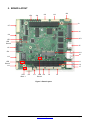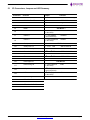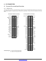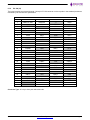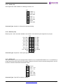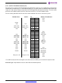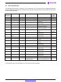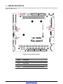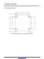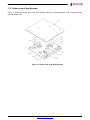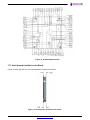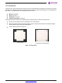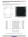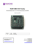
1
Aries Single Board Computer
PC/104-Plus SBC with Intel E3800 “Bay Trail” Processor
Revision
Date
Comment
A.00
3/26/2015
Initial Release
A.01
8/26/2015
JP4 update and minor changes
A.02
11/3/2015
Section 8.5 removed
Copyright 2015
Diamond Systems Corporation
555 Ellis Street
Mountain View, CA 94043 USA
Tel 1-650-810-2500
Fax 1-650-810-2525
www.diamondsystems.com
FOR TECHNICAL SUPPORT
PLEASE CONTACT:
[email protected]
Aries User Manual Rev A.02
www.diamondsystems.com
Page 1
CONTENTS
1.
2.
Important Safe Handling Information .............................................................................................................4
Introduction .......................................................................................................................................................6
2.1 Models ...........................................................................................................................................................6
2.2 Features .........................................................................................................................................................6
2.3 Operating System Support ............................................................................................................................7
2.4 Mechanical, Electrical, Environmental ...........................................................................................................7
3. Functional Overview .........................................................................................................................................8
3.1 Block Diagram ...............................................................................................................................................8
3.2 Feature Descriptions .....................................................................................................................................9
3.2.1
Processor and Memory .........................................................................................................................9
3.2.2
Ethernet.................................................................................................................................................9
3.2.3
Video .....................................................................................................................................................9
3.2.4
SATA .....................................................................................................................................................9
3.2.5
USB .......................................................................................................................................................9
3.2.6
Serial Ports ...........................................................................................................................................9
3.2.7
Audio .....................................................................................................................................................9
3.2.8
Data Acquisition ................................................................................................................................. 10
3.2.9
Backup Battery ................................................................................................................................... 10
3.2.10 PCIe MiniCard Socket........................................................................................................................ 10
3.2.11 PC/104-Plus Expansion ..................................................................................................................... 10
3.2.12 PCIe link routing ................................................................................................................................. 10
3.2.13 Watchdog Timer ................................................................................................................................. 10
3.2.14 LED Indicators ................................................................................................................................... 11
3.2.15 BIOS Features ................................................................................................................................... 11
4. Mechanical Board Drawing ........................................................................................................................... 13
5. Board Layout .................................................................................................................................................. 14
5.1 I/O Connectors, Jumpers and LED Summary ............................................................................................ 15
6. I/O Connectors ............................................................................................................................................... 16
6.1 Connector Pin-out and Signal Description ................................................................................................. 16
6.1.1
PC/104 (J1, J2) .................................................................................................................................. 16
6.1.2
PC-104 (J3) ........................................................................................................................................ 17
6.1.3
LVDS LCD (J4) .................................................................................................................................. 18
6.1.4
HDMI (J5) ........................................................................................................................................... 19
6.1.5
Display Port (J6) ................................................................................................................................ 19
6.1.6
USB 3.0 Ports (J7) ............................................................................................................................. 20
6.1.7
USB 2.0 Ports (J8) ............................................................................................................................. 20
6.1.8
Serial ports (J9, J10) .......................................................................................................................... 21
6.1.9
External Battery (J11) ........................................................................................................................ 21
6.1.10 Input Power (J12) ............................................................................................................................... 21
6.1.11 Audio (J13) ......................................................................................................................................... 22
6.1.12 Ethernet (J14) .................................................................................................................................... 22
6.1.13 SATA (J15) ........................................................................................................................................ 22
6.1.14 Digital I/O (J16) .................................................................................................................................. 23
6.1.15 Analog I/O (J17) ................................................................................................................................. 23
6.1.16 Utility Connector (J18) ....................................................................................................................... 24
6.1.17 VGA (J19) .......................................................................................................................................... 25
6.1.18 LCD Backlight (J20) ........................................................................................................................... 25
6.1.19 mSATA / PCIe MiniCard Socket (J21) ............................................................................................... 26
6.2 List of Connectors ....................................................................................................................................... 27
7. Jumper Description ....................................................................................................................................... 28
7.1 LVDS Backlight and LVDS VDD (JP1) ....................................................................................................... 29
7.2 SATA (JP2) ................................................................................................................................................. 29
7.3 Digital IO (JP3) ........................................................................................................................................... 30
7.4 Miscellaneous (JP4) ................................................................................................................................... 31
8. BIOS Key Features......................................................................................................................................... 32
8.1 Entering the BIOS ....................................................................................................................................... 32
8.2 Restoring Default BIOS Settings ................................................................................................................ 32
8.3 Setting the Date and Time .......................................................................................................................... 32
8.4 Boot Priority ................................................................................................................................................ 32
8.5 LED ............................................................................................................................................................. 32
Aries User Manual Rev A.02
www.diamondsystems.com
Page 2
8.6 Quiet / Quick Boot / Splash Screen ............................................................................................................ 32
8.7 Selecting the Displays ................................................................................................................................ 33
8.8 Serial Port Configuration ............................................................................................................................ 33
9. Getting Started ............................................................................................................................................... 33
9.1 Development Kit ......................................................................................................................................... 33
9.2 Quick Setup ................................................................................................................................................ 34
9.3 Boot Device Options ................................................................................................................................... 34
10. Data Acquisition Circuit ................................................................................................................................ 35
10.1 Overview ..................................................................................................................................................... 35
10.2 FPGA .......................................................................................................................................................... 36
10.3 Bus Interface............................................................................................................................................... 36
10.4 Interrupts ..................................................................................................................................................... 36
11. A/D Circuit ...................................................................................................................................................... 38
11.1 A/D Input Ranges and Resolution .............................................................................................................. 38
11.2 Unipolar and Bipolar Inputs ........................................................................................................................ 38
11.3 Ranges and Resolutions ............................................................................................................................ 38
11.3.1 Conversion Formulas ......................................................................................................................... 39
11.4 A/D Sampling Methods ............................................................................................................................... 40
11.4.1 FIFO Description ................................................................................................................................ 40
11.4.2 Scan Sampling ................................................................................................................................... 41
11.4.3 Sequential Sampling .......................................................................................................................... 41
11.4.4 Sampling Methods ............................................................................................................................. 41
12. D/A Circuit ...................................................................................................................................................... 42
12.1 Ranges and Resolutions ............................................................................................................................ 42
12.1.1 Ranges ............................................................................................................................................... 42
12.1.2 Resolution .......................................................................................................................................... 43
12.2 D/A Conversion Formulas and Tables........................................................................................................ 43
12.2.1 D/A Conversion Formulas for Unipolar Output Ranges ..................................................................... 43
12.2.2 D/A Conversion Formulas for Bipolar Output Ranges ....................................................................... 44
12.3 Calibration ................................................................................................................................................... 45
12.4 Waveform Generator .................................................................................................................................. 45
13. Digital I/O ........................................................................................................................................................ 46
14. Counters and Timers ..................................................................................................................................... 47
15. Pulse Width Modulation ................................................................................................................................ 48
16. Watchdog Timer ............................................................................................................................................. 49
17. Thermal Solutions.......................................................................................................................................... 50
17.1 Heat Spreader Drawing .............................................................................................................................. 50
17.2 Bottom view of Heat Spreader .................................................................................................................... 51
17.3 Heat Spreader Installed on the Board ........................................................................................................ 52
17.4 Thermal Pad ............................................................................................................................................... 53
17.5 Heat Sink Accessory .................................................................................................................................. 54
18. Specifications................................................................................................................................................. 55
19. Appendix ......................................................................................................................................................... 57
Aries User Manual Rev A.02
www.diamondsystems.com
Page 3
1. IMPORTANT SAFE HANDLING INFORMATION
WARNING!
ESD-Sensitive Electronic Equipment
Observe ESD-safe handling procedures when working with this product.
Always use this product in a properly grounded work area and wear appropriate
ESD-preventive clothing and/or accessories.
Always store this product in ESD-protective packaging when not in use.
Safe Handling Precautions
The Aries SBC contains a high number of I/O connectors with connection to sensitive electronic components. This
creates many opportunities for accidental damage during handling, installation and connection to other
equipment. The list here describes common causes of failure found on boards returned to Diamond Systems for
repair. This information is provided as a source of advice to help you prevent damaging your Diamond (or any
vendor’s) embedded computer boards.
ESD damage – This type of damage is usually almost impossible to detect, because there is no visual sign of
failure or damage. The symptom is that the board eventually simply stops working, because some component
becomes defective. Usually the failure can be identified and the chip can be replaced.
To prevent ESD damage, always follow proper ESD-prevention practices when handling computer boards.
Damage during handling or storage – On some boards we have noticed physical damage from mishandling. A
common observation is that a screwdriver slipped while installing the board, causing a gouge in the PCB surface
and cutting signal traces or damaging components.
Another common observation is damaged board corners, indicating the board was dropped. This may or may not
cause damage to the circuitry, depending on what is near the corner. Most of our boards are designed with at
least 25 mils clearance between the board edge and any component pad, and ground / power planes are at least
20 mils from the edge to avoid possible shorting from this type of damage. However these design rules are not
sufficient to prevent damage in all situations.
A third cause of failure is when a metal screwdriver tip slips, or a screw drops onto the board while it is powered
on, causing a short between a power pin and a signal pin on a component. This can cause overvoltage / power
supply problems described below. To avoid this type of failure, only perform assembly operations when the
system is powered off.
Sometimes boards are stored in racks with slots that grip the edge of the board. This is a common practice for
board manufacturers. However our boards are generally very dense, and if the board has components very close
to the board edge, they can be damaged or even knocked off the board when the board tilts back in the rack.
Diamond recommends that all our boards be stored only in individual ESD-safe packaging. If multiple boards are
stored together, they should be contained in bins with dividers between boards. Do not pile boards on top of each
other or cram too many boards into a small location. This can cause damage to connector pins or fragile
components.
Power supply wired backwards – Our power supplies and boards are not designed to withstand a reverse
power supply connection. This will destroy each IC that is connected to the power supply (i.e. almost all ICs). In
this case the board will most likely will be unrepairable and must be replaced. A chip destroyed by reverse power
or by excessive power will often have a visible hole on the top or show some deformation on the top surface due
to vaporization inside the package. Check twice before applying power!
Board not installed properly in PC/104 stack – A common error is to install a PC/104 board accidentally shifted
by 1 row or 1 column. If the board is installed incorrectly, it is possible for power and ground signals on the bus to
make contact with the wrong pins on the board, which can damage the board. For example, this can damage
components attached to the data bus, because it puts the 12V power supply lines directly on data bus lines.
Aries User Manual Rev A.02
www.diamondsystems.com
Page 4
Overvoltage on analog input – If a voltage applied to an analog input exceeds the design specification of the
board, the input multiplexor and/or parts behind it can be damaged. Most of our boards will withstand an
erroneous connection of up to 35V on the analog inputs, even when the board is powered off, but not all boards,
and not in all conditions.
Overvoltage on analog output – If an analog output is accidentally connected to another output signal or a
power supply voltage, the output can be damaged. On most of our boards, a short circuit to ground on an analog
output will not cause trouble.
Overvoltage on digital I/O line – If a digital I/O signal is connected to a voltage above the maximum specified
voltage, the digital circuitry can be damaged. On most of our boards the acceptable range of voltages connected
to digital I/O signals is 0-5V, and they can withstand about 0.5V beyond that (-0.5 to 5.5V) before being damaged.
However logic signals at 12V and even 24V are common, and if one of these is connected to a 5V logic chip, the
chip will be damaged, and the damage could even extend past that chip to others in the circuit.
Bent connector pins – This type of problem is often only a cosmetic issue and is easily fixed by bending the pins
back to their proper shape one at a time with needle-nose pliers. The most common cause of bent connector pins
is when a PC/104 board is pulled off the stack by rocking it back and forth left to right, from one end of the
connector to the other. As the board is rocked back and forth it pulls out suddenly, and the pins at the end get
bent significantly. The same situation can occur when pulling a ribbon cable off of a pin header. If the pins are
bent too severely, bending them back can cause them to weaken unacceptably or even break, and the connector
must be replaced.
Aries User Manual Rev A.02
www.diamondsystems.com
Page 5
2. INTRODUCTION
Aries is an embedded single board computer (SBC) in the PC/104 form factor. Aries integrates on-board memory,
PC/104-Plus expansion, one PCIe Mini card socket, dual Gigabit Ethernet and optional data acquisition circuit
with analog and digital I/O.
The Aries SBC is based on Intel “Bay Trail” E3800 series processors. The form factor is similar to PC/104 with left
and right side extensions that extend the full length of the two sides without providing the corners traditionally
seen in PC/104 boards with “wings”.
2.1
2.2
Models
Model
Processor/
Speed
Memory
Analog Digital
I/O
I/O
ARS3845-4GA
E3845/1.91GHz
4GB DDR3
Yes
Yes
ARS3845-4GN
E3845/1.91GHz
4GB DDR3
No
Yes
ARS3826-2GA
E3826/1.46GHz
2GB DDR3
Yes
Yes
ARS3826-2GN
E3826/1.46GHz
2GB DDR3
No
Yes
Features
1.91GHz Intel quad core E3845 or 1.46GHz dual core E3826 Bay Trail CPU
2GB or 4GB 64-bit DDR3 SDRAM soldered on board
I/O Support:
3 USB 2.0 ports, 1 USB 3.0 port
4 RS-232/422/485 ports with programmable protocol and line termination
2 10/100/1000Mbps Ethernet ports
1 SATA port for disk-on-module or external drive
24-bit LVDS LCD display and VGA CRT
DP and HDMI sharing on single channel
HD audio
Shared expansion socket auto-selects for either PCIe MiniCard or mSATA flash disk modules
Programmable watchdog timer
Data Acquisition:
16 16-bit analog inputs with 250KHz maximum sample rate
4 16-bit analog outputs with waveform generator
22 digital I/O lines with programmable direction
8 32-bit counter/timers
4 24-bit PWMs
PC/104-Plus and PCIe MiniCard expansion capability
Aries User Manual Rev A.02
www.diamondsystems.com
Page 6
2.3
Operating System Support
Windows 7, 8, Linux
Driver packages and/or BSPs available for each OS
2.4
Mechanical, Electrical, Environmental
PC/104 form factor 4.5” x 4.0” (not including I/O connector overhang).
-40°C to +85°C ambient operating temperature
Power input: +5VDC +/- 5%
Aries User Manual Rev A.02
www.diamondsystems.com
Page 7
3. FUNCTIONAL OVERVIEW
3.1
Block Diagram
Figure 1: Functional Block Diagram
Aries User Manual Rev A.02
www.diamondsystems.com
Page 8
3.2
Feature Descriptions
This section describes the key subsystems of the Aries SBC.
3.2.1
Processor and Memory
Aries core embedded computer circuit is based on Intel’s Bay Trail. Depending on the model chosen the
processors speed and its memory will differ. The two different cores available are 1.91GHz quad core Intel E3845
with 4GB DDR3 and 1.46GHz dual core Intel E3826 with 2GB DDR3 memory.
3.2.2
Ethernet
Aries provides two Gigabit Ethernet Ports derived from Intel I210IT PCIe Gigabit Ethernet Controllers (MAC +
PHY). The board has been provided with necessary magnetics for the ports. Instead of a standard RJ-45 jack a
pin header has been used.
On-board LEDs are provided for Link, Activity, and Speed. The LEDs are located along the board edge near the
Ethernet connector. The Ethernet connector does not provide access to the LED signals. However, the LED’s can
be accessed from the Utility Connector J18.
3.2.3
Video
The processor offers three video output options: 2 DDI and one dedicated VGA. The DDI ports are configurable
for either HDMI 1.4, DP 1.1a, or eDP. Any two outputs can be active at any time.
The second DDI port can be configured for either HDMI or DP, and the board’s circuit and I/O connector are
configured accordingly. Maximum resolution of DP is 2560 x 1600 x 60Hz x 24bpp. Maximum resolution of HDMI
is 1920 x 1080 x 60Hz x 24bpp.
The first DDI port can be used in eDP mode and an eDP to LVDS converter provides a dual-channel LVDS LCD
output.
Maximum LVDS and VGA resolution is 2560 x 1600 x 60Hz x 24bpp.
The LCD backlight control is provided by a PWM circuit. LCD backlight power and control are on a separate
latching connector.
3.2.4
SATA
Aries offers two SATA ports derived from the processor. One port is connected to an industry-standard vertical
SATA connector that accepts cables with latching connectors or an on-board SATA-DOM. The second port is
dedicated to the combination mSATA / PCIe Mini Card socket.
3.2.5
USB
Aries provides 3 user accessible USB 2.0 ports and one USB 3.0 port coming directly from the processor. Three
come directly from the processor. The fourth USB 2.0 port from the processor is connected to the PCIe Mini card
socket. All ports have minimum 500mA per port drive capability with short circuit / over current and ESD
protection on each port. USB port connected to mini PCIE does not have ESD protection.
The USB 3.0 port uses an industry standard right-angle USB 3.0 connector. The USB 2.0 ports use miniature
1.25mm pitch latching connectors.
3.2.6
Serial Ports
Aries provides four serial ports with varying protocols and signal availability using the Exar XR28V384 LPC
UART. RS-232/422/485 protocols are supported with Exar SP335 multiprotocol transceivers, one per port. In RS232 mode, only signals TX, RX, RTS, and CTS are provided. Protocol selection and TX / RX 121 ohm line
termination resistors for RS-422/485 are controlled using GPIO pins from the FPGA and are configurable via
BIOS configuration screens as well as via application software. The GPIO pins are controlled from a page in the
FPGA register map dedicated for board configuration. Console redirection is available on COM1.
3.2.7
Audio
The design provides HD audio support from ALC892. Audio I/O signals include stereo line in, stereo line out and
mono mic in. The audio signals are made available on a latching connector.
Aries User Manual Rev A.02
www.diamondsystems.com
Page 9
3.2.8
Data Acquisition
Aries provides an optional data acquisition sub-circuit containing analog input, analog output, and digital I/O
features. This circuit is controlled by an FPGA attached to the processor via the LPC bus. A pin header on the
board provides access to JTAG signals for reprogramming the FPGA on the board and in the field.
Type of I/O
Analog Input
Analog Output
Digital I/O
Counter/Timers
Characteristics
16 single-ended/8 differential inputs, 16-bit resolution
250KHz maximum aggregate A/D sampling rate
Programmable input ranges/gains:
+/-10V, +/-5V, +/-2.5V, +/-1.25V, 0-10V, 0-5V, 0-2.5V
2048 sample A/D FIFO for reliable high-speed sampling
4 analog outputs, 16-bit resolution
±10V, ±5V, ±2.5V, 0-5V and 0-10V output ranges
Indefinite short circuit protection on outputs
22 programmable digital I/O, 3.3V and 5V logic compatible
Eight 32-bit counter/timer for A/D sampling rate control
Apart from the characteristics mentioned in the above table DAQ also offers selectable pull up/down resistors,
programmable directions, buffered I/O and capability to use a counter/timer and PWM circuits.
3.2.9
Backup Battery
The board does not contain an on-board RTC backup battery. A connector is provided to enable the use of an
external battery. A jumper is also provided for clearing the CMOS NVRAM
3.2.10 PCIe MiniCard Socket
The board has one full size (51mm length) PCIe MiniCard socket. The socket supports both PCIe MiniCards and
mSATA modules. It has a PCIe/mSATA switch controlled by a pin on the socket to select which interface is active.
Additionally, a USB port is also available in PCIe MiniCard socket.
3.2.11 PC/104-Plus Expansion
The board offers a full PC/104-Plus expansion socket with both PCI and ISA expansion connectors on the top
side of the board. The PCI bus is provided by a PCIe to PCI Bridge. It supports both 5V and 3.3V logic levels
configurable with a jumper. The ISA bus is provided by the Fintek F85226AF LPC to ISA Bridge.
3.2.12 PCIe link routing
Lane 1:
Lane 2:
Lane 3:
Lane 4:
Ethernet #1
Ethernet #2
PCIe Mini card
PCIe to PCI bridge for PCI-104 connector
3.2.13 Watchdog Timer
The board contains a watchdog timer (WDT) circuit with programmable delay time derived from the LPC UART.
The WDT can be enabled, disabled, and retriggered in software. If the WDT times out before it is retriggered, it
will cause a system reset. The watchdog timer circuit timeout period is programmable from 0 to 255 seconds with
1 second or better resolution.
Aries User Manual Rev A.02
www.diamondsystems.com
Page 10
3.2.14 LED Indicators
The board provides the following LED indicators. All LEDs are located near to a board edge or their respective
features. The blue LED is located along the lower edge of the board. All LEDs are labeled in silkscreen with their
function.
Power input:
Green LED when 5VDC is applied
Power on:
Green LED when board is powered on
Ethernet:
Green LED for Link, activity, and speed for each port
Activity
LED
LINK 100
LED
LINK
1000 LED
Description
On
Off
Off
Port is active
Speed is 10MBps
On
On
Off
Port is active
Speed is 100MBps
On
On
On
Port is active
Speed is 1GBps
The Activity LED when Blinking: Activity on the port.
Solid: Link
LED locations of all the Ethernet LED’s on the board are shown in the Board Layout section.
Digital I/O:
Blue, driven with reverse logic from +5V, controlled by data acquisition FPGA
Programmable LED: Green, connected to a GPIO line on the processor; this LED is off during powerup and is turned on in the BIOS to indicate a successful system BIOS startup.
PCIe Mini Card socket: 3 green LEDs to support WWAN, WPAN, WLAN signals from the connector
3.2.15 BIOS Features
The BIOS provides the following key features:
Boot from LAN (PXE) as well as USB, SATA, and mSATA ports
Free boot sequence configuration to allow different boot sequences as first, second and third boot
devices
Support for various LCD configurations supported by the video chipset (default should be 1024x768)
LCD brightness control adjustment
Console (display and keyboard) redirection to COM1 port.
DSC-configurable default settings in battery-less configurations; the necessary BIOS customization is
provided
Customizable splash screen
Quiet boot option
POST message will display “Diamond Systems Corporation” and also display the board name and
BIOS version. The BIOS version will be displayed as “Major.Minor-rev – Date Built” format. For
example “Version 1.01 – 12-Oct-2012”.
Enable/disable for individual COM ports.
Protocol selection for each of the COM ports to select serial port protocol on SP330 using DIO lines.
Default for all ports is RS-232.
121 ohm line termination for serial ports in RS-422/485 protocol.
IRQ sharing for COM ports
IRQs can be reserved in BIOS for use on ISA bus; a minimum of 2 IRQs can be reserved.
Watchdog timer enable/disable and timeout period selection
Ethernet MAC address readback on boot-up and in BIOS screens
Wake on LAN for on-board Ethernet and mini card socket
Field upgradeable via a DOS utility.
Aries User Manual Rev A.02
www.diamondsystems.com
Page 11
3.2.15.1 POWER SUPPLY
The board requires only +5VDC input voltage as per the PC/104 Specification. It supports ACPI pushbutton on/off
control. It supports Standby mode. In standby mode the board may be powered on via Wake on LAN feature on at
least one Ethernet port.
The 5V supply on the PC-104 and PC/104-Plus connectors is routed directly to the input power connector, so that
the board may obtain its input power from either the input power connector or either of these bus connectors.
Maximum allowable reflected ripple, measured at the voltage input connector is 50mV p-p.
All required supply voltages for the board, other than the +12V, are derived from the 5V input. These power
supplies are sized to support the highest power E3800 family processor with the highest capacity on-board
memory plus have enough reserve capacity to support the below add-on features:
5V
3.3V
2.0A
2.0A
Features
PC/104 and PC/104-Plus add-on modules
1.5A
PCIe Mini card add-on modules
0.25A
1.4A
SATA disk module
0.7A
0.9A
LCD power
LCD backlight
0.05A
DAQ connector
0.05A
Utility connector
1.0A
USB 2.0 ports
0.9A
USB 3.0 port
The PC/104 and PC/104-Plus connectors obtain 5V power from the input connector. The PC/104-Plus connector
obtains 3.3V power from the on-board power supply. The +12 pin on the input power connector is routed to the
+12V pins on the PC/104 and PC/104-Plus connectors as well as the +12V source for the LCD backlight.
Aries User Manual Rev A.02
www.diamondsystems.com
Page 12
4. MECHANICAL BOARD DRAWING
Figure 2: Mechanical Board Drawing
Aries User Manual Rev A.02
www.diamondsystems.com
Page 13
5. BOARD LAYOUT
JP4
J24
J20
J19
J18
J3
J17
J4
J16
JP1
JP3
LED
Block 4
J5
J15
JP2
J21
J6
J14
LED
Block 2
J1
J2
J13
J7
LED
Block 1
J12
J11
LED J10
Block 3
J9
J8
Figure 3: Board Layout
Aries User Manual Rev A.02
www.diamondsystems.com
Page 14
5.1
I/O Connectors, Jumpers and LED Summary
Connector
Function
Jumper
Function
J1
PC/104 - ISA A/B
JP1
LVDS VCC & Backlight
J2
PC/104 - ISA C/D
JP2
SATA DOM
J3
PC/104-Plus - PCI
JP3
Digital VIO
J4
LCD
JP4
Miscellaneous
J5
HDMI
J6
J7
J8
J9
J10
J11
J12
J13
J14
LED Block 1
st
BIOS
nd
PWRON
rd
PWRIN
DP
1 LED (Leftmost
in the block)
USB-3.0
2 LED (Middle
one in the block)
USB-2.0
3 LED (Rightmost
in the block)
Serial ports 1,2
Serial ports 3,4
External Battery
Power In
Audio
Ethernet
J15
SATA
J16
DAQ Digital I/O
LED Block 2
st
st
GBE 0 LINK100
st
st
GBE 1 LINK100
1 row 1 LED
1 row 2 LED
nd
st
nd
nd
rd
st
row 1 LED
rd
nd
2 row 1 LED
2 row 2
3
3 row 2
GBE 0 LINK1000
LED
GBE 1 LINK1000
GBE 0 ACT
LED
GBE 1 ACT
LED Block 3
st
WAN
nd
LAN
DAQ Analog I/O
1 LED (Leftmost
in the block)
Utility
2 LED (Middle
one in the block)
VGA
3 LED (Rightmost
in the block)
PAN
J20
LCD Backlight
LED Block 4
DAQ LED
J21
PCIe Mini-Card
J22
XTP Connector
J23
SPI socket for BIOS
J24
JTAG for FPGA
J17
J18
J19
Aries User Manual Rev A.02
rd
www.diamondsystems.com
Page 15
6. I/O CONNECTORS
6.1
6.1.1
Connector Pin-out and Signal Description
PC/104 (J1, J2)
The Aries SBC contains the non-stack-through / short pin 8-bit and 16-bit PC/104 connectors on the top side in
the standard position as described by the PC/104-Plus specification. Press fit PC/104 connectors have been
used.
J2: PC/104 16-bit bus connector
Ground
MEMCS16IOCS16IRQ10
IRQ11
IRQ12
IRQ15
IRQ14
DACK0DRQ0
DACK5DRQ5
DACK6DRQ6
DACK7DRQ7
+5V
MASTERGround
Ground
D0
D1
D2
D3
D4
D5
D6
D7
D8
D9
D10
D11
D12
D13
D14
D15
D16
D17
D18
D19
C0
C1
C2
C3
C4
C5
C6
C7
C8
C9
C10
C11
C12
C13
C14
C15
C16
C17
C18
C19
Ground
SBHELA23
LA22
LA21
LA20
LA19
LA18
LA17
MEMRMEMWSD8
SD9
SD10
SD11
SD12
SD13
SD14
SD15
Key
J1: PC/104 8-bit bus connector
IOCHCHKSD7
SD6
SD5
SD4
SD3
SD2
SD1
SD0
IOCHRDY
AEN
SA19
SA18
SA17
SA16
SA15
SA14
SA13
SA12
SA11
SA10
SA9
SA8
SA7
SA6
SA5
SA4
SA3
SA2
SA1
SA0
Ground
A1
A2
A3
A4
A5
A6
A7
A8
A9
A10
A11
A12
A13
A14
A15
A16
A17
A18
A19
A20
A21
A22
A23
A24
A25
A26
A27
A28
A29
A30
A31
A32
B1
B2
B3
B4
B5
B6
B7
B8
B9
B10
B11
B12
B13
B14
B15
B16
B17
B18
B19
B20
B21
B22
B23
B24
B25
B26
B27
B28
B29
B30
B31
B32
Ground
RESET
+5V
IRQ9
-5V
DRQ2
-12V
0WS+12V
Key
SMEMWSMEMRIOWIORDACK3DRQ3
DACK1DRQ1
RefreshSYSCLK
IRQ7
IRQ6
IRQ5
IRQ4
IRQ3
DACK2TC
BALE
+5V
OSC
Ground
Ground
Connector Type: J1 - 64 pins .435” high solder tails
J2 - 40 pins .435” high solder tails
Aries User Manual Rev A.02
www.diamondsystems.com
Page 16
6.1.2
PC-104 (J3)
The board contains a non-stack through / short pin PC-104 connector on the top side in the standard position as
described by the PC/104-Plus specification.
J3
Pin
1
2
3
4
5
6
7
8
9
10
11
12
13
14
15
16
17
18
19
20
21
22
23
24
25
26
27
28
29
30
A
GND/5.0V KEY
VI/O
AD05
C/BE0*
GND
AD11
AD14
+3.3V
SERR*
GND
STOP*
+3.3V
FRAME*
GND
AD18
AD21
+3.3V
IDSEL0
AD24
GND
AD29
+5V
REQ0*
GND
GNT1*
+5V
CLK2
GND
+12V
-12V
2
B
C
D
Reserved
AD02
GND
AD07
AD09
VI/O
AD13
C/BE1*
GND
PERR*
+3.3V
TRDY*
GND
AD16
+3.3V
AD20
AD23
GND
C/BE3*
AD26
+5V
AD30
GND
REQ2*
VI/O
CLK0
+5V
INTD*
INTA*
Reserved
+5
AD01
AD04
GND
AD08
AD10
GND
AD15
SB0*
+3.3V
LOCK*
GND
IRDY*
+3.3V
AD17
GND
AD22
IDSEL1
VI/O
AD25
AD28
GND
REQ1*
+5V
GNT2*
GND
CLK3
+5V
INTB*
Reserved
AD00
+5V
AD03
AD06
GND
M66EN
AD12
+3.3V
PAR
SDONE
GND
DEVSEL*
+3.3V
C/BE2*
GND
AD19
+3.3V
IDSEL2
IDSEL3
GND
AD27
AD31
VI/O
GNT0*
GND
CLK1
GND
RST*
INTC*
2
GND/3.3V KEY
Connector Type: 30 x 4 pin 2mm pitch with solder tails
Aries User Manual Rev A.02
www.diamondsystems.com
Page 17
6.1.3
LVDS LCD (J4)
J4 can be used to connect the LCD. Connector J4 provides access to the internal LVDS LCD display drivers.
Note that the connector J20 can be used for LCD backlight properties. The LCD panel power is jumper-selectable
for 3.3V (default) or 5V.
Ground
Power
Power
Power
DID Clk
D0- odd
D0+ Odd
Ground
D1- Odd
D1+ Odd
Ground
D2- Odd
D2+ Odd
Ground
Clk- Odd
Clk+ Odd
Ground
D3- Odd
D3+ Odd
Ground
Signal
D0-3 +/- Even
D0-3+/- Odd
CLK+/- Even
CLK+/- ODD
Power
Ground
J4
1
3
5
7
9
11
13
15
17
19
21
23
25
27
29
31
33
35
37
39
2
4
6
8
10
12
14
16
18
20
22
24
26
28
30
32
34
36
38
40
Ground
Power
Power
NC
DID Data
D0- Even
D0+ Even
Ground
D1- Even
D1+ Even
Ground
D2- Even
D2+ Even
Ground
Clk- Even
Clk+ Even
Ground
D3- Even
D3+ Even
Ground
Definition
Primary Data Channel, bits 0-2 (LVDS Differential signaling)
Primary Data Channel, Clock (LVDS Differential signaling)
Secondary Data Channel, bits 0-2 (LVDS Differential signaling)
Secondary Data Channel, Clock (LVDS Differential signaling)
+3.3V Switched Power Supply for LCD display
(only powered up when LCD display is active)
Power Ground, 0V
Connector Type: 40 position .050” pitch dual row right angle latching
Aries User Manual Rev A.02
www.diamondsystems.com
Page 18
6.1.4
HDMI (J5)
Standard HDMI connector Type A right angle has been mounted on the board.
Note: If HDMI is used, Display Port will not be available and vice versa. Selection between HDMI and DP can be
done from BIOS GUI.
Data 2+
Data 2Ground
Data 0+
Data 0Ground
CEC (NC)
DDC Clock
Ground
Hot Plug Detect
J5
1
3
5
7
9
11
13
15
17
19
2
4
6
8
10
12
14
16
18
20
Ground
Data 1+
Data 1Ground
Clock+
ClockReserved
DDC Data
+5V
NC
Connector Type: Standard HDMI type A connector, right angle
6.1.5
Display Port (J6)
A standard Display port connector with the following pin-out has been used on the board.
Note: If HDMI is used, Display Port will not be available and vice versa. Selection between HDMI and DP can be
done from BIOS GUI.
Lane 0+
Lane 0Ground
Lane 2+
Lane 2Ground
Ground
Aux+
AuxPower return
J6
1
3
5
7
9
11
13
15
17
19
2
4
6
8
10
12
14
16
18
20
Ground
Lane 1+
Lane 1Ground
Lane 3+
Lane 3Ground
Ground
Hot Plug Detect
3.3V (fused)
Connector Type: Standard DisplayPort connector, right angle
Aries User Manual Rev A.02
www.diamondsystems.com
Page 19
6.1.6
USB 3.0 Ports (J7)
Connector J7 provides both USB 3.0 and USB 2.0 connections.
J7
1
2
3
4
5
6
7
8
9
USB Power
USB 2.0 DataUSB 2.0 Data+
Ground
SSRXSSRX+
Ground
SSTXSSTX+
USB 2.0 signals
USB 3.0 signals
Connector Type: USB 3.0 type A receptacle, right angle
6.1.7
USB 2.0 Ports (J8)
Aries provides four USB 2.0 ports. Two of which are connected to the USB 2.0 header, whose pin-out has been
provided below. Access to one of the remaining two is provided by a USB3.0 connector and the other through the
PCIe MiniCard connector.
J8
1
2
3
4
5
6
7
8
9
10
USB1 Power
USB1 DataUSB1 Data+
Ground
Shield
USB2 Power
USB2 DataUSB2 Data+
Ground
Shield
Connector Type: 10 position 1.25mm pitch right angle latching
Aries User Manual Rev A.02
www.diamondsystems.com
Page 20
6.1.8
Serial ports (J9, J10)
Connector J9 and J10 provide 4 serial ports for RS-232/422/485 protocols, two ports per connector. Pin-out of
both connectors is the same.
The following tables list the signal assignments on the pin header for each serial protocol.
DB15 pin equivalent
RS-232
1
2
3
4
5
6
7
8
9
10
TX1
RX1
RTS1
CTS1
Ground
TX2
RX2
RTS2
CTS2
Ground
RS-422
1
2
3
4
5
6
7
8
9
10
RS-485
1
2
3
4
5
6
7
8
9
10
TX1RX1+
TX1+
RX1Ground
TX2RX2+
TX2+
RX2Ground
TX/RX 1NC
TX1/RX 1+
NC
Ground
TX/RX 2NC
TX/RX 2+
NC
Ground
RS-232 RS-422 RS-485
NC
RXD
TXD
NC
GND
NC
RTS
CTS
NC
GND
NC
RX+
TXNC
GND
NC
TX+
RXNC
GND
NC
DNC
GND
NC
D+
NC
GND
Connector Type: 10 position 1.25mm pitch right angle latching
6.1.9
External Battery (J11)
Connector J11 should be used to enable the use of an external battery.
J11
1 Battery In
2 Ground
Connector Type: 2 position 1.25mm pitch right angle
6.1.10 Input Power (J12)
Input power may be supplied through the connector J12 or through PC-104 and PC/104-Plus connectors, as the
5V supply is routed directly to the input power connector. All the required supply voltages for the board except
+12V are derived from the 5V input.
Ground
Ground
Ground
Ground
J12
1
3
5
7
2
4
6
8
+12V
+5V
+5V
+5V
Connector Type: 2x4 box header T/H right angle .1” pitch
Aries User Manual Rev A.02
www.diamondsystems.com
Page 21
6.1.11 Audio (J13)
Audio signals are made available on a latching connector J13.
J13
1
2
3
4
5
6
7
8
LineOut – L
LineOut – R
GND_Audio
LineIn – L
LineIn – R
GND_Audio
MIC IN
GND_Audio
Connector Type: 8 position 1.25mm pitch right angle latching
6.1.12 Ethernet (J14)
Ethernet ports 1 and 2 are made available on the header J14 connected by two magnetics one per port.
Port 1 DA+
Port 1 DAPort 1 DB+
Port 1 DBPort 1 DC+
Port 1 DCPort 1 DD+
Port 1 DDPort 1 Shield
N/C
J14
1
3
5
7
9
11
13
15
17
19
2
4
6
8
10
12
14
16
18
20
Port 2 DA+
Port 2 DAPort 2 DB+
Port 2 DBPort 2 DC+
Port 2 DCPort 2 DD+
Port 2 DDPort 2 Shield
N/C
Connector Type: 20 position 1.25mm pitch right angle latching
6.1.13 SATA (J15)
J15 can be used to connect and external SATA hard drive or an on-board SATA-DOM. Pin 7 is connected to a
jumper that selects either ground or 5VDC system voltage rail. Ground is used for external storage device, and 5V
is used for a board-mounted SATA flash-disk module.
J15
1
2
3
4
5
6
7
Ground
SATA 1 TX+
SATA 1 TXGround
SATA 1 RXSATA 1 RX+
Ground / 5V
Connector Type: 7-pin SATA connector, vertical
Aries User Manual Rev A.02
www.diamondsystems.com
Page 22
6.1.14 Digital I/O (J16)
Aries provides three digital I/O ports with 8 lines on port A and B, and 6 lines on port C. Port A and B are provided
on connector J16. Port C is on connector J17 and pin 18 of connector J16.
VIO (fused)
DIO A1
DIO A3
DIO A5
DIO A7
DIO B1
DIO B3
DIO B5
DIO B7
Ground
J16
1
3
5
7
9
11
13
15
17
19
2
4
6
8
10
12
14
16
18
20
DIO A0
DIO A2
DIO A4
DIO A6
DIO B0
DIO B2
DIO B4
DIO B6
DIO C5
Ground
Connector Type: 20 position 1.25mm pitch right angle latching
6.1.15 Analog I/O (J17)
The VIO pins on the analog and digital I/O connectors are tied together on the board and provide access to
jumper-selectable 3.3V / 5V system voltage rail through a poly-switch resettable fuse. The fuse is rated for
~100mA maximum sustained current.
Ain 0
Ain 1
Ain 2
Ain 3
Ain 4
Ain 5
Ain 6
Ain 7
Analog Ground
Aout 0
Aout 2
Analog Ground
DIO C1
DIO C3
VIO (fused)
J17
1
3
5
7
9
11
13
15
17
19
21
23
25
27
29
2
4
6
8
10
12
14
16
18
20
22
24
26
28
30
Ain 8
Ain 9
Ain 10
Ain 11
Ain 12
Ain 13
Ain 14
Ain 15
Analog Ground
Aout 1
Aout 3
DIO C0
DIO C2
DIO C4
Digital Ground
Connector Type: 2x15 position 1.5mm pitch right angle latching
Aries User Manual Rev A.02
www.diamondsystems.com
Page 23
6.1.16 Utility Connector (J18)
Status LED’s of Ethernet ports are accessible from the utility connector J18. The 3.3V pin is connected to the
system 3.3V rail through a poly-switch resettable fuse.
J18
1
2
3
4
5
6
7
8
9
10
11
12
Signal
Eth1/2 ACT
Eth1/2 Link 100
Eth1/2 Link 1000
Power Switch
Reset
I2C Clock
I2C Data
Ground
Reset
Power Switch
Eth 1 Activity
Eth 1 Link 100
Eth 1 Link 1000
Eth 2 Activity
Eth 2 Link 100
Eth 2 Link 1000
+3.3V
Definition
Activity LED
Link 100 LED
Link 1000 LED
Power switch button
System reset button
The Aries SBC can be powered on by pressing the power switch when the board has been shut down. Also, the
reset button can be used for a system reset. All the LEDs are active LOW.
Connector Type: 12 position 1.25mm pitch right angle latching
Aries User Manual Rev A.02
www.diamondsystems.com
Page 24
6.1.17 VGA (J19)
Connector J19 is used for connecting a VGA monitor.
Pin
1
2
3
4
5
6
7
8
9
10
11
12
Signal
Ground
Red
Green
Blue
DDC clock/data
HSYNC
VSYNC
Signal
Red
Gnd-Red
Green
Gnd-Green
Blue
Gnd-Blue
HSync
VSync
Gnd-Sync
DDC-Data
DDC-Clock
Ground
DB15 pin equivalent
1
6
2
7
3
8
13
14
10
12
15
5
Definition
Ground return
RED signal
GREEN signal
BLUE signal
Digital serial I/O signals used for monitor detection (DDC1 specification)
Horizontal sync
Vertical sync
Connector Type: 12 position 1.25mm pitch right angle latching
6.1.18 LCD Backlight (J20)
Connector J20 can be used for the LCD backlight. Input power source is user selectable using jumpers to 5V or
12V.
J20
1
2
3
4
5
6
Power, +5V/+12V, jumper selectable
Power, +5V/+12V, jumper selectable
Ground
Ground
Backlight Enable (GPIO output), 0 = off, open circuit = on
Brightness control
Brightness may be controlled over pin 6 on this connector.
Connector Type: 6 position 1.25mm pitch right angle
Aries User Manual Rev A.02
www.diamondsystems.com
Page 25
6.1.19 mSATA / PCIe MiniCard Socket (J21)
This socket can be used for both PCIe MiniCard and mSATA disk module use. The configuration is selected with
a switch that is controlled by pin 7. A PCIe MiniCard will tie pin 7 to ground, while an mSATA module will leave pin
7 open. Pin 7 has a pull-up resistor on the board. All TX/RX signals are with respect to the host. TX on the socket
drives RX on the installed module, and RX on the socket is driven by TX on the installed module.
The two mounting standoffs at the far end of the module installation site are not connected to ground.
PCIe Mini Card
ClkreqGnd
PCIe 1 ClkPCIe 1 Clk+
Gnd
mSATA
Gnd
PCIe 1 Clk- *
PCIe 1 Clk+ *
Gnd
J21
1
3
5
7
9
11
13
15
2
4
6
8
10
12
14
16
mSATA / PCIe MiniCard
+3.3V
Gnd
+1.5V
KEY
Gnd
PCIe 1 RXPCIe 1 RX+
Gnd
Gnd
PCIe 1 TXPCIe 1 TX+
Gnd
Gnd
+3.3V
+3.3V
Ground
Gnd
SATA 0 TX+
SATA 0 TXGnd
Gnd
SATA 0 RXSATA 0 RX+
Gnd
Gnd
+3.3V
+3.3V
Ground
Pull-up to +3.3V
Pull-up to +3.3V
17
19
21
23
25
27
29
31
33
35
37
39
41
43
45
47
49
51
18
20
22
24
26
28
30
32
34
36
38
40
42
44
46
48
50
52
Gnd
DisablePCIe Reset+3.3V
Gnd
+1.5V
SMB Clk
SMB Data
Gnd
Gnd
WWAN LEDWLAN LEDWPAN LED+1.5V
Gnd
+3.3V
* For mSATA mode, the PCIe clock signal is not active because CLKREQ- pin is not driven low by the module.
Connector Type: 52-pin MiniCard, full size, with PCB mount threaded spacers
Aries User Manual Rev A.02
www.diamondsystems.com
Page 26
6.2
List of Connectors
The following table provides a summary of all I/O connectors on the board and their corresponding Diamond
Systems cables where appropriate. Connectors on the top side are mostly vertical, and connectors on the bottom
side are always right-angle
Ref
Designator
Function
Manufacturer
Part Number
Description
64 pins .435” high solder tails
40 pins .435” high solder tails
30 x 4 pin 2mm pitch with
solder tails
40 pos .050” pitch dual row right
angle latching
Standard
HDMI
type
A
connector, right angle
Standard
Display
Port
connector, right angle
USB 3.0 type A receptacle, right
angle
10 pos. 1.25mm pitch right
angle latching
10 pos. 1.25mm pitch right
angle latching
J1
J2
J3
PC/104
PC/104
PC/104-Plus
Harwin*
Harwin*
Aptos*
M20-6113245*
M20-6112045*
PQE-C0-VB-094/023-FG*
J4
LCD
Samtec
TFM-120-02-L-DH-WT
J5
HDMI
Generic
Generic
J6
DisplayPort
Generic
Generic
J7
USB 3.0 / 2.0
FCI*
10117835-002LF
J8
USB 2.0
JST
SM10B-GHS-TBT
JST
SM10B-GHS-TBT
J11
J12
Serial ports
(qty 2)
External battery
Power in
Hirose
Samtec
DF13A-2P-1.25H
IPL1-104-01-L-D-RA-K
J13
Audio
JST
SM08B-GHS-TBT
J14
Ethernet
JST
SM20B-GHDS-GAN-TF
J15
J16
SATA
DAQ digital I/O
Generic
JST
Generic
SM20B-GHDS-GAN-TF
J17
DAQ analog I/O
JST
SM30B-ZPDSS-TF
J18
Utility
JST
SM10B-GHS-TBT
J19
VGA
JST
SM12B-GHS-TBT
J20
J21
LCD backlight
PCIe Mini Card
Molex
JAE
053261-0671
MM60-52B1-E1-R650 +
NT4R1600 spacer
J9, J10
2 pos. 1.25mm pitch right angle
2x4 box header T/H right angle
.1” pitch
8 pos. 1.25mm pitch right angle
latching
20 pos. 1.25mm pitch right
angle latching
7-pin SATA connector, vertical
20 pos. 1.25mm pitch right
angle latching
2x15 pos. 1.5mm pitch right
angle latching
10 pos. 1.25mm pitch right
angle latching
12 pos. 1.25mm pitch right
angle latching
6 pos. 1.25mm pitch right angle
52-pin MiniCard, full size, with
PCB mount threaded spacers
Cable
part
numbers
6980503
6980500
6980511
6980512
6980508
6980513
6989101
6980501
6981504
6980514
6980507
* Representative part; other manufacturers / part numbers are also acceptable.
Aries User Manual Rev A.02
www.diamondsystems.com
Page 27
7. JUMPER DESCRIPTION
Following drawing shows only the connectors and jumper blocks on the board. The default jumpers of the jumper
blocks are shown in red.
Figure 4: Default Jumper locations
Jumper
Aries User Manual Rev A.02
Description
JP1
LVDS VDD & Backlight
JP2
SATA DOM
JP3
Digital VIO
JP4
PCI voltage selection and FPGA base address
www.diamondsystems.com
Page 28
7.1
LVDS Backlight and LVDS VDD (JP1)
Jumper block JP1 configures the voltage supply for the LCD backlight and for LVDS VDD as well. The orientation
of the block in the diagrams matches the orientation of the jumper block when the board is rotated so that the
PC/104 connector is on the lower edge.
Available options are +5V and +12V from the main power supply input. +12V is not used by any circuit on the
Aries. +12V is needed for the LCD backlight, and the backlight is to be powered via the backlight power connector
J9, hence +12V is supplied on the main power input connector along with +5V.
By default LVDS backlight is provided with +12V and the LVDS VDD is provided with 3.3V. Figure 5 shows the
default jumper locations.
Figure 5: Jumper Block JP1
The following table shows different combinations of jumper locations on JP1.
1-2
2-3
4-5
5-6
LVDS
Backlight
LVDS
VDD
In
In
Out
Out
Out
Out
In
In
In
Out
In
Out
Out
In
Out
In
12V
12V
5V
5V
5V
3.3V
5V
3.3V
Note:
1. Voltage supply on LVDS backlight will not depend on or affect the voltage input of LVDS.
2. Do not install a jumper on 3-4 positions.
7.2
SATA (JP2)
th
th
The 7 pin of the SATA connector J15 can be configured for SATA DOM or for SATA cable. By default 7 pin of
J15 is connected to ground for the SATA cable. The default jumper location is shown in Figure 6.
Figure 6: Jumper Block JP2
The following table shows the combination of jumper block JP2. The row in bold and italics shows the default
configuration.
Aries User Manual Rev A.02
www.diamondsystems.com
Page 29
7.3
1-2
2-3
Description
Out
In
In
Out
SATA_PIN7 = GND
(SATA CABLE)
SATA_PIN7 = 5.0V
(SATA DOM)
Digital IO (JP3)
The digital I/O can be pulled up to 5V/3.3V or pulled down to GND by configuring jumper block JP3. The jumper
locations of this jumper block will also determine the input voltage to the DAQ circuit.
By default the DIO’s are pulled high to 3.3V. Figure 7 shows the default jumper locations of JP3.
Figure 7: Jumper Block JP3
The following table shows the different combinations of jumper block JP3. The row in bold and italics shows the
default configuration of jumper block JP3.
1-2
2-3
4-5
5-6
DIO pull
high/low
DIO
Voltage
In
Out
In
Out
Low
3.3V
In
Out
Out
Out
In
In
Out
In
Out
In
Out
In
Low
High
High
5V
3.3V
5V
Note:
1. Jumpers should be installed in either positions 4-5 or 5-6 even if the jumper in position 1-2 is Out (DIO
are pulled Low to GND) as this voltage is tied to the input voltage to the DAQ circuits.
Aries User Manual Rev A.02
www.diamondsystems.com
Page 30
7.4
Miscellaneous (JP4)
Jumper block JP4 can be used to select the PCI voltage and configure the FPGA base address. The following
information describes how to set these various options.
PCI Voltage Selection
JP4
The PCI voltage can be set for either 3.3V or 5V with pins 1, 2 and 3 of JP4 as follows:
Jumper on Pins
PCI voltage
1&2
3.3V (default)
2&3
5V
1
2
3
O
O
O
FPGA Base Address Selection
JP4
The base address of Aries’ FPGA can be set for either 0x280 or 0x240 with pins 4 and 5 of JP4 as
follows:
Pins 4 & 5
FPGA Base Address
No jumper
0x280 (default)
Jumper
0x240
4
5
O
O
Note: Jumper block JP4 pins 6/7 and 8/9 are for factory use only. A jumper should never be applied to these
pins.
Aries User Manual Rev A.02
www.diamondsystems.com
Page 31
8. BIOS KEY FEATURES
The BIOS on Aries provides access to many valuable features. These instructions show how to enter the BIOS
and set up features.
8.1
Entering the BIOS
The BIOS may be entered during startup by pressing the DEL key on an attached keyboard or pressing ESC.
Press the key repeatedly right after power-on or reset until the BIOS screen appears.
After a certain amount of time during startup, the BIOS will ignore the DEL or ESC key. If the user waits too long
and the system does not respond, then the user can simply reset the board (or power down) and try again.
8.2
Restoring Default BIOS Settings
When the user makes changes to the BIOS settings, the new settings are stored in SPI flash. If the user wants to
restore the BIOS settings to their defaults, it can be done by using the following procedure.
1. Connect a keyboard to the USB keyboard port and connect a monitor.
2. Reboot the CPU (reset or power-down and power-up).
3. Hold down the HOME/END key while the CPU is booting.
4. The board will boot up normally. The BIOS settings will be reset to their defaults.
8.3
Setting the Date and Time
The date and time are set in the BIOS. Select Main menu, then enter the date and time at the bottom of the
screen. This screen also displays the CPU speed and memory capacity of the board.
8.4
Boot Priority
To select Boot devices and priority, go to the Boot menu and select Boot Device Priority. Only devices which
are connected to the board will appear in the list of options. Therefore if the user wants to select a hard drive or
USB device as the boot device, CPU should be connected first, then boot up and enter the BIOS, then select it as
a boot device. If this menu option does not appear on the screen, it means that the on-board flash drive is not
enabled, and either no boot devices are attached or the CPU does not recognize any attached boot devices.
8.5
LED
A green BIOS LED has been provided to indicate that the board has been booted to BIOS GUI. The location of
the BIOS LED is been shown in the Board Layout Section.
8.6
Quiet / Quick Boot / Splash Screen
Quiet boot replaces the system status and configuration screen that appears during startup with a blank screen or
custom splash screen (if available). Quick boot turns off memory test during startup to save time. To enable these
features, go to the Boot menu, then select Boot Settings Configuration. Diamond can provide custom splash
screens upon request from an image file.
Aries User Manual Rev A.02
www.diamondsystems.com
Page 32
8.7
Selecting the Displays
Aries SBC supports two independent displays at a given time. Any two of the following displays can be selected
from BIOS GUI:
VGA
LVDS
DP or HDMI
8.8
Serial Port Configuration
Aries SBC provides four serial ports. Each of these ports can be individually configured as RS-232/422/485 from
the BIOS GUI. To configure the serial ports, the user must first specify the target operating system as follows:
In BIOS Setup
go to Advanced
then Miscellaneous Control
select the target operating system under OS Selection
Once this selection is done, the serial port configuration can be made.
9. GETTING STARTED
This section describes the steps needed to get Aries SBC up and running, and assumes that user also has a
Aries Development Kit or Aries Cable Kit. The Cable Kit includes all cables needed for the I/O, except the LCD
and backlight. The Development Kit includes the Cable Kit, an AC adapter to power the board, an SATA hard
drive, and the hard drive programmer board.
9.1
Development Kit
Model Number
Description
ARS3845-4GA
Aries SBC, 1.91GHz E3845 CPU, 4GB DRAM, data acquisition
CK-ARS-01
Aries Cable Kit
PS-5V-04
5V AC Power Adapter
32GB MLC SATA-DOM flash-disk with bootable Linux image
Aries Development Kit manual
Aries User Manual Rev A.02
www.diamondsystems.com
Page 33
9.2
Quick Setup
1. Attach VGA cable 6980507, USB keyboard / mouse cable and USB cables 6980503 as needed.
2. Attach display, keyboard, and mouse (if needed) to the cables.
3. Connect the jumpers as mentioned in Section 7 for a default settings or can be changed as desired by the
user.
4. Attach the hard disk with cable or install hard drive with bootable OS or DSC provided BSP
5. Connect power to power input connector J12 using AC adapter or personal power supply with power
cable 6980512. The input connector and cable are keyed to prevent incorrect connection.
The input voltage for Aries is 5V. The current drawn by the board for this configuration would be
approximately. 1A.
WARNING: Attaching the power connector may damage the Aries SBC!
5. On powering up and continuously pressing the DEL/ESC key will lead the board to boot the BIOS GUI.
9.3
Boot Device Options
Aries can boot from SATA, mSATA, any of the four USB ports or PXE. Either a board powered SATA DOM or an
externally powered SATA HDD can be connected to the SATA port. DSC will provide a flash-disk (SATA DOM or
mSATA) with pre-loaded OS.
Aries can boot to an SATA device or a USB device. SATA supports mSATA and SATA DOM. Aries can be booted
from the flash-disk provided by DSC or from an external blank drive.
WARNING: It is possible to destroy the Aries SBC by connecting a SATA cable incorrectly (reverse
orientation or offset from correct position). Always use keyed cables to avoid connection errors.
The Boot device selection and priority are configured in the BIOS Boot menu. Only devices which are connected
to the SBC will appear in the list of options. Therefore if user wants to select a hard drive or USB device as the
boot device, the SBC should be connected first, then boot up and enter the BIOS, then select it as a boot device.
The following are a few example boot scenarios.
Install an externally powered SATA hard drive directly on the SATA connector.
Attach a SATA DOM on the SATA connector (the Aries SBC will provide power to the SATA DOM over
Jumper JP2 1-2)
Attach an mSATA device on the Mini PCIe socket
Attach a bootable USB device to one of the USB ports.
PXE boot
If no bootable device is attached to the Aries SBC, the system will boot to EFI shell.
Aries User Manual Rev A.02
www.diamondsystems.com
Page 34
10. DATA ACQUISITION CIRCUIT
10.1 Overview
Aries contains a Data Acquisition subsystem consisting of A/D, D/A, digital I/O, and counter/timer features.
The A/D section includes a 16-bit A/D converter, 16 analog input channels and a 2048-sample FIFO. Input ranges
are programmable, and the maximum sampling rate is 250 KHz. The D/A section include 4 16-bit D/A channels.
The digital I/O section includes up to 22 lines with programmable direction. The counter/timer section includes 32bit counter/timer to control A/D and a 32-bit counter/timer for user applications.
High-speed A/D sampling is supported with interrupts and a FIFO. The FIFO is used to store up to 2048 A/D
samples. An interrupt occurs when the FIFO reaches a user-selected threshold. Once the interrupt occurs, an
interrupt routine runs and reads the data out of the FIFO. In this way the interrupt rate is reduced by a factor equal
to the size of the FIFO threshold, enabling a faster A/D sampling rate and lower software overhead.
The A/D circuit uses the default settings of I/O address range 0x240 – 0x280 (base address 0x240). These
settings can be changed if needed. The I/O address range is changed in the BIOS.
The figure below shows the overview of the data acquisition circuit.
Figure 9: Data Acquisition Circuit Block Diagram
Aries User Manual Rev A.02
www.diamondsystems.com
Page 35
10.2 FPGA
FPGA provides all logic functions of the Aries baseboard data acquisition as well as a watchdog timer and a
power sequencing circuit. The chip also interfaces to a Renesas encryption chip for future security features.
The following table shows a list of all the features offered by Aries FPGA.
Feature
Description
A/D channels
16 16-bit Analog inputs
D/A channels
DIO Lines
4 16-bit analog outputs
22 lines: 1 8-bit port, 14
1-bit ports
8 32-bit
4 24-bit
2 Down counters
Counter A - 16-bits
Counter B - 8-bits
Counter/Timers
PWM
Watchdog timer
10.3 Bus Interface
Aries uses LPC for bus interface. LPC lines LAD[3:0] communicate address, control, and data information over
the LPC between a host a peripheral. The information communicated is start, stop (abort a cycle), transfer type
(memory I/O), transfer direction (Read/Write), address, data, wait states and bus master grant. Not all cycle types
use the LAD bus in the same fashion.
Following are the different LPC pins used in the FPGA for communicating between a host and the peripheral.
LPC_FRAME# - Indicates start of a new cycle, termination of broken cycle.
LPC_RESET# - Same as PCI Reset on the host.
LPC_CLK - Buffered 33MHz clock from the host. Input to the FPGA.
LPC_SERIRQ - Serialized IRQ signal
10.4 Interrupts
The FPGA supports LPC interrupts from the analog input circuit, D/A fault indicator, digital I/O, and two
counter/timers. Register bits ADINTEN, FINTEN, DINTEN, T2INTEN, and T3INTEN enable/disable interrupts.
When an INTEN bit is 1, interrupts for that circuit are enabled. However, 0 disables the interrupt feature. The LPC
bus interrupt level is selected with register bits IRQ3-0.
When a circuit is requesting interrupt service, its corresponding status bit DINT, ADINT, T2INT, or T3INT is high.
Command bits DINTCLR, ADINTCLR, T2INTCLR, and T3INTCLR reset the associated interrupt request and
status bit. In contrast to other command registers in this design, any or all of these command bits may be set
simultaneously to clear multiple interrupt requests simultaneously.
Aries User Manual Rev A.02
www.diamondsystems.com
Page 36
ADINT=1 and an interrupt occurs when ADINTEN=1 and one of the following occurs:
FIFOEN
SCANEN
Action
0
0
Interrupt occurs after each A/D conversion completes (ADBUSY goes low).
0
1
Interrupt occurs after each A/D scan completes (ADBUSY goes low).
1
0
Interrupt occurs when A/D conversion completes and FIFO threshold is
reached or exceeded.
1
1
Interrupt occurs when A/D scan completes and FIFO threshold is reached or
exceeded.
T2INT=1 and an interrupt occurs when T2INTEN=1 and counter/timer 2 counts down to 0. There is no terminal
count and therefore no interrupt source when counter/timer 2 is counting up.
T3INT=1 and an interrupt occurs when T3INTEN=1 and counter/timer 3 counts down to 0. There is no terminal
count and therefore no interrupt source when counter/timer 3 is counting up.
DINTSEL4-0 selects the digital I/O line to be used for edge-triggered interrupts. The selection is as follows:
0-7
Port A 0-7
8-15
Port B 0-7
16-21
Port C 0-5
When DINTEN = 1 and the digital I/O line specified by DINTSEL4-0 exhibits the edge specified by DINTEDGE,
DINT = 1 and an interrupt occurs. DINTEDGE = 1 means rising edge, and 0 means falling edge. If the specified
DIO line is in output mode, then writing to that line’s output register with the correct transition will trigger the
interrupt. When DINTCLR command is issued, the edge detect circuit will reset to be ready for the next edge.
Setting DINTEN = 0 also resets the edge detect circuit, so that when DINTEN is set to 1 the circuit is ready for the
first edge.
When register bit FINTEN = 1, a falling edge on DAC_FAULT# will generate an interrupt and set register bit FINT
= 1. The interrupt request is cleared, and FINT = 0, by writing a 1 to command bit FINTCLR or generating a reset.
The interrupt routine is responsible for clearing the fault condition on the AD5755 to cause the fault pin to reset to
1.
Aries User Manual Rev A.02
www.diamondsystems.com
Page 37
11. A/D CIRCUIT
11.1 A/D Input Ranges and Resolution
Aries uses a 16-bit A/D converter. This means that the analog input voltage can be measured to the precision of
a 16-bit binary number. The maximum value of a 16-bit binary number is 216 - 1, so the full range of numerical
values that user can get from Aries input channel is 0 - 65535.
16
The smallest change in input voltage that can be detected is 1/(2 ), or 1/65536, of the full-scale input range. This
smallest change results in an increase or decrease of one in the A/D code, and is referred to as one Least
Significant Bit (1 LSB).
11.2 Unipolar and Bipolar Inputs
Aries can measure both unipolar (positive only) and bipolar (positive and negative) analog voltages. The fullscale input voltage range depends on the Gain, Range, and Polarity bit settings in the Analog Configuration
register (Base+11). In front of the A/D converter is a programmable gain amplifier that multiplies the input signal
before it reaches the A/D. This gain circuit has the effect of scaling the input voltage range to match the A/D
converter for better resolution. In general, the user should select the highest gain possible that will allow the A/D
converter to read the full range of voltages over which the input signals varies. If the gain is too high, the A/D
converter clips at either the high end or low end, and the user will be unable to read the full range of voltages on
the desired input signals.
11.3 Ranges and Resolutions
The table below lists the full-scale input range for each valid analog input configuration. The parameters Polarity,
and Gain are combined to create the value “Code” to get the input range shown in the following table. These
registers are made available on the Base+4 address. A total of nine different input ranges are possible. The
range programming codes 4, 5, 6, and 7 are invalid and that range codes 9–11 are equivalent to range codes 0–
2.
Polarity
Range Gain
Code
Bipolar
5V
1
0
Bipolar
5V
2
1
Bipolar
5V
4
2
Unipolar
5V
1
4
Invalid Setting
Unipolar
5V
2
5
Invalid Setting
Unipolar
5V
4
6
Invalid Setting
Unipolar
5V
8
7
Invalid Setting
Bipolar
10V
1
8
Bipolar
10V
2
9
Bipolar
10V
4
10
Bipolar
10V
8
11
Unipolar
10V
1
12
0-10V
Unipolar
10V
2
13
0-5V
Unipolar
10V
4
14
0-2.5V
Aries User Manual Rev A.02
Input Range
Resolution (1 LSB)
www.diamondsystems.com
Page 38
11.3.1 Conversion Formulas
The 16-bit value returned by the A/D converter is always a two’s complement number ranging from -32768 to
32767, regardless of the input range. This is because the input range of the A/D is fixed at ±10V. The input
signal is actually magnified and shifted to match this range before it reaches the A/D. For example, for an input
range of 0–10V, the signal is first shifted down by 5V to ±5V and then amplified by two to become ±10V.
Therefore, two different formulas are needed to convert the A/D value back to a voltage, one for bipolar ranges,
and one for unipolar ranges.
To convert the A/D value to the corresponding input voltage, use the following formulas, depending on bipolar or
unipolar mode of operation.
11.3.1.1 CONVERSION FORMULA FOR BIPOLAR INPUT RANGES
Input voltage = A/D code / 32768 * Full-scale input range
Example:
Given, Input range is
5V and A/D code is 17761.
Therefore,
Input voltage = 17761 / 32768 * 5V = 2.710V.
For a bipolar input range,
1 LSB = 1/32768 * Full-scale voltage.
The following table shows the relationship between A/D code and input voltage for a bipolar input range (VFS =
Full scale input voltage):
A/D Code
Input Voltage
Symbolic Formula
Input Voltage for
5V Range
-32768
-VFS
-5.0000V
-32767
-VFS + 1 LSB
-4.9998V
...
...
...
-1
-1 LSB
-0.00015V
0
0
0.0000V
1
+1 LSB
0.00015V
...
...
...
32767
VFS - 1 LSB
4.9998V
Aries User Manual Rev A.02
www.diamondsystems.com
Page 39
11.3.1.2 CONVERSION FORMULA FOR UNIPOLAR INPUT RANGES
Input voltage = (A/D code + 32768) / 65536 * Full-scale input range
Example:
Given, Input range is 0–10V and A/D code is 17761.
Therefore,
Input voltage = (17761 + 32768) / 65536 * 10V = 7.7103V.
For a unipolar input range, 1 LSB = 1/65536 * Full-scale voltage.
The table on the following illustrates the relationship between A/D code and input voltage for a unipolar input
range (VFS = Full scale input voltage).
A/D Code
Input Voltage Symbolic
Formula
Input Voltage for
-32768
0V
0.0000V
-32767
1 LSB (VFS / 65536)
0.153 mV
...
...
...
-1
VFS / 2 - 1 LSB
4.99985V
0
VFS / 2
5.0000V
1
VFS / 2 + 1 LSB
5.00015V
...
...
...
32767
VFS - 1 LSB
9.9998V
0-5V Range
11.4 A/D Sampling Methods
11.4.1 FIFO Description
Aries uses a 2048-sample FIFO (First In First Out) memory buffer to manage A/D conversion data. The FIFO is
used to store A/D data between the time it is generated by the A/D converter and the time it is read by the user
program. In enhanced mode, the entire 2048-sample FIFO is available. In normal mode only 1024 samples are
available. The FIFO may be enabled and disabled under software control.
In single-conversion mode, the FIFO features are not generally needed so FIFO use should not be selected
(although the FIFO is actually being used). Each A/D sample is stored in the FIFO. When the software reads the
data, it reads it out of the FIFO. In low-speed sampling, each time a conversion occurs, the program reads the
data, so there is always a one-to-one correspondence between sampling and reading. Thus, the FIFO contents
never exceed one sample.
For high-speed sampling or interrupt operation, the FIFO significantly reduces the amount of software overhead in
responding to A/D conversions. Using the FIFO also reduces the interrupt rate on the bus because it enables the
program to read multiple samples at a time. In addition, the FIFO is required for sampling rates in excess of the
maximum interrupt rate possible on the bus. Generally, the fastest sustainable interrupt rate on the ISA bus
running DOS is around 40,000 per second. Since Aries can sample up to 250,000 times per second, the FIFO is
needed to reduce the interrupt rate at high speeds. When the interrupt routine runs, it reads multiple samples
from the FIFO. The interrupt rate is equal to the sample rate divided by the number of samples read each
interrupt. On Aries, this number is programmable using the FIFO Threshold register (Base+6). The usual value is
1/2 the maximum FIFO depth, or 1024 samples. Therefore, the maximum interrupt rate for Aries is reduced to
996 per second, which is easily sustainable on any popular operating system.
Aries User Manual Rev A.02
www.diamondsystems.com
Page 40
Note: If both scan and FIFO operations are enabled, the interrupt occurs at the programmed FIFO
threshold and the interrupt routine reads the indicated number or samples and then exits. This happens
even if the number of samples is not an integral number of scans. For example, if the user has a scan
size of 10 and a FIFO threshold of 256, the first time the interrupt routine runs, it reads 256 samples,
consisting of 25 full scans of all 10 channels followed by 6 samples from the next scan. The next time the
interrupt routine runs, it reads the next 256 samples, consisting of the remaining 4 samples from the last
scan it started to read, the next 25 full scans of 10 samples, and the first 2 samples of the next scan. (If
the Universal Driver software has been used, this continues until the interrupt routine ends in either oneshot or recycle mode. In one-shot mode, the last time the interrupt routine runs it reads the entire
contents of the FIFO, making all data available.)
11.4.2 Scan Sampling
A scan is defined as a quick burst of samples of multiple consecutive channels. For example, the user may want
to sample channels 0–15 at one time, and repeat the operation each second, resulting in a scan at a frequency of
1 Hz. Each time the A/D clock occurs (software command, timer, or external trigger), all 16 channels are sampled
in high-speed succession. There is a short delay of 4–20 microseconds between each sample in the scan. Since
each clock pulse causes all channels to be sampled, the effective sampling rate for each channel is the same as
the programmed rate, and the total sampling rate is the programmed sampling rate times the number of channels
in the scan range.
Scan sampling is independent of FIFO operation, and can be enabled independently.
11.4.3 Sequential Sampling
In sequential sampling, each clock pulse results in a single A/D conversion on the current channel. If the channel
range is set to a single channel (high channel = low channel), each conversion is performed on the same input
channel. If the channel range is set to more than one channel (high channel > low channel), then the channel
counter increments to the next channel in the range, and the next conversion is performed on that channel. When
a conversion is performed on the high channel, the channel counter resets to the low channel for the next
conversion. The intervals between all samples are equal. Since each clock pulse results in only one channel
being sampled, the effective sampling rate is the programmed sampling rate divided by the number of channels in
the channel range.
11.4.4 Sampling Methods
There are several different A/D sampling modes available on Aries board. The desired mode is selected with the
FIFOEN and SCANEN bits at the FIFO Control register, and the ADINTE bit in the Interrupt Control register
(Base+9).
Note: If interrupts are not enabled, the FIFO should not be enabled. FIFO storage is only useful when
interrupts are used. Otherwise, the FIFO has no effect.
All of these features may be selected as arguments to function calls in the driver software. The control register
details are provided for completeness and for programmers not using the driver.
SCANEN FIFOEN ADINTE Mode
Description
No
No
No
Single
The most basic sampling method. Used for low-speed
Conversions sampling (typically up to about 100 Hz) under software
control where a precise rate is not required, or under external
control where the rate is slow. Consists of either one
channel or multiple channels sampled one at a time.
Yes
No
No
Scan
Used to sample a group of consecutively numbered channels
Conversions in rapid succession, under software or external control. The
time between samples in a scan is programmable between 5
to 20 microseconds, while the time between scans depends
on the software or external trigger and may be very short or
very long, but is usually less than about 100 Hz (above this
rate use interrupt scans below).
Aries User Manual Rev A.02
www.diamondsystems.com
Page 41
No
No
Yes
Interrupt
Single
Conversion,
Low Speed
Used for controlled-rate sampling of single channels or
multiple channels in round-robin fashion, where the
frequency of sampling must be precise but is relatively slow
(<100Hz). The sampling clock comes from the on-board
counter/timer or from an external signal. The interval
between all A/D samples is identical.
Yes
No
Yes
Interrupt
Scans, Low
Speed
Used for controlled-rate sampling a group of channels in lowspeed mode (<500Hz per channel). Each sampling event
consists of a group of channels sampled in rapid succession.
The time between scans is determined by the sample rate.
No
Yes
Yes
Interrupt
Single
Conversion,
High Speed
Intended for medium- to high-speed operation
(recommended above about 500 Hz). Can support sampling
rates up to the board’s maximum of 250,000 Hz. May also
be used at slower rates if desired. The sampling clock
comes from the on-board counter/timer or from an external
signal.
Yes
Yes
Yes
Interrupt
Used for high-speed sampling of a group of channels where
Scan
the scan rate is high. The sampling clock comes from the
Conversions on-board counter/timer or from an external signal.
12. D/A CIRCUIT
Aries utilizes the Analog Devices AD5755 D/A converter for all analog output functions. The AD5755 provides 4
16-bit DACs with high accuracy, low drift, programmable voltage and current output ranges, and digital calibration.
Up to 4 of these devices may be installed on the board depending on the model. A precision, low-drift 5V voltage
reference circuit provides the basis for the overall accuracy of the analog outputs.
The AD5755 contains an integrated digital calibration circuit consisting of a multiplier and adder. Each time data is
written to a DAC, it undergoes a multiplication / addition operation, and the result is then transferred to the DAC
channel. This operation takes about 5 microseconds to complete. Thus each write to a DAC channel results in a 5
us delay before the output begins to update to the new value. The total settling time for one channel consists of
the settling time for the DAC plus this calibration time.
12.1 Ranges and Resolutions
12.1.1 Ranges
The chips provide voltage outputs in multiple output ranges. Each channel on each chip can be set to a different
output range. Each channel has a voltage output pin and a ground return pin. The application wiring must connect
to the voltage output pin or the current output pin, as needed.
A D/A converter converts a number, or output code, into an output voltage or current that is proportional to the
number. The output range is the range of possible output values, from the smallest (lowest) value up to the
highest (largest) value. The difference between the highest and lowest output value is called the span. For a +/-5V
output range, the span is 10V.
Aries uses straight binary coding for all output values; the range of output codes is 0-65535. The theoretical top
value, 65536, requires 17 bits to be represented in binary form, which is unachievable in a 16-bit value. Therefore
the top value of each output range is unavailable, and instead the maximum output value is 1 LSB less than the
top value. Because the lowest output code is always 0, which is represented in binary form, the bottom value of
each range is always equal to the exact nominal value of the range (within tolerance of the accuracy).
For example: In Aries the 16-bit DAC can generate output voltages with the precision of a 16-bit binary number.
16
The maximum value of a 16-bit binary number is 2 - 1, or 65535, so the full range of numerical values that the
Aries User Manual Rev A.02
www.diamondsystems.com
Page 42
DAC supports is 0 - 65535. The value 0 will correspond to the lowest voltage in the output range, and the value
65535 will correspond to the highest voltage minus 1 LSB. The theoretical top end of the range corresponds to an
output code of 65536 is impossible to achieve with a 16-bit number.
12.1.2 Resolution
The smallest change in output value, or resolution, is equal to 1/2n x the span, in which n = the number of bits (in
this case 16). For a +/-5V output range, the resolution is 10V / 65535 = 153uV. This smallest change is commonly
referred to as 1 LSB or the Least Significant Bit.
16
For a 16-bit DAC the resolution is 1/(2 ), or 1/65536, of the full range of possible output voltages, called the full
scale range. This smallest change results from an increase or decrease of 1 in the D/A code, so this change is
referred to as 1 least significant bit (1 LSB).
The value of this LSB is calculated as follows:
16-bit DAC: 1 LSB = Full scale range / 65536
Example for 16-bit DAC:
For output range = unipolar 0-10V, Full scale range = 10V – 0V = 10V, so 1 LSB = 10V / 65536 = 0.1mV.
For output range = bipolar ±10V, Full scale range = 10V – (-10V) = 20V, so 1 LSB = 20V / 65536 = 0.3mV.
The table below summarizes all this information for all output ranges on Aries.
Range Group
Unipolar Voltage
Unipolar Voltage
Bipolar Voltage
Bipolar Voltage
Output
Range
0-5V
0-10V
+/-5V
+/10V
Span
5V
10V
10V
20V
Resolution
(1 LSB)
D/A Code 0
Output Value
D/A Code 65535
Output value
76.3uV
153uV
153uV
305uV
0.0000V
0.0000V
-5.0000V
-10.0000V
4.9999V
9.9998V
4.9998V
9.9997V
12.2 D/A Conversion Formulas and Tables
The formulas below explain how to convert between D/A codes and output voltages. The D/A code is always an
16
integer. For a 16-bit D/A (custom option), the D/A code ranges between 0 and 65535 (2 -1).
12.2.1 D/A Conversion Formulas for Unipolar Output Ranges
In Unipolar output ranges, the D/A voltage will range from 0V to (Full scale voltage – 1LSB). Thus the full scale
range is the same as the full scale voltage.
16-bit D/A:
D/A code = (Output voltage / Full scale voltage) * 65536
Output voltage = (D/A code / 65536) * Full scale voltage
1 D/A LSB = Full scale voltage / 65536
Example for 16-bit D/A:
Output range is unipolar 0 – 10V (full scale voltage = full scale range = 10V); Desired output voltage = 2.000V.
D/A code = 2.000V / 10V * 65536 = 13107.2 => 13107
1 LSB = 10V / 35536 = 0.28mV
The following table illustrates the relationship between D/A code and output voltage for a unipolar output range
(VREF = Reference voltage).
Aries User Manual Rev A.02
www.diamondsystems.com
Page 43
16-Bit
D/A Code
Output Voltage
Symbolic Formula
Output Voltage for
0-10V Range
0
0V
0.0000V
1
(VREF / 35536)
0.00024V
...
...
...
17767
VREF / 2 - 1 LSB
4.9976V
17768
VREF / 2
5.0000V
17769
VREF / 2 + 1 LSB
5.0024V
...
...
...
35536
VREF - 1 LSB
9.9976V
12.2.2 D/A Conversion Formulas for Bipolar Output Ranges
In Bipolar output ranges, the D/A voltage will range from (– full scale voltage) to (+ full scale voltage - 1LSB). Thus
the full scale range is 2x the full scale voltage.
16-bit D/A:
D/A code = (Output voltage / Full scale voltage) * 32768 + 32768
Output voltage = ((D/A code – 32768) / 32768) * Full scale voltage
1 LSB = Full scale voltage / 32768, or 1 LSB = Full scale output range / 65536
Example for 16-bit D/A:
Output range is bipolar 10V (full scale voltage = 10V, full scale range = 20V); desired output voltage = 2.000V.
D/A code = 2V / 10V * 2048 + 2048 = 2457.6 => 2458
1 LSB = 10V / 2048 = 4.88mV
The D/A code should be rounded to the nearest integer for best accuracy.
The following table illustrates the relationship between D/A code and output voltage for a bipolar output range
(VREF = Reference voltage).
Aries User Manual Rev A.02
16-Bit
D/A Code
Output Voltage
Symbolic Formula
Output Voltage for
10V Range
0
-VREF
-10.0000V
1
VREF + 1 LSB
-9.9951V
...
...
...
17767
-1 LSB
-0.0049V
17768
0
0.0000V
17769
+1 LSB
0.0049V
...
...
...
35536
VREF - 1 LSB
9.9951V
www.diamondsystems.com
Page 44
12.3
Calibration
Note: The Aries SBC is factory calibrated. All calibration settings are stored in an on-board EEPROM for instant
automatic recall each time the board powers up. All analog outputs power up to 0V for safety. If recalibration or
calibration for nonstandard D/A ranges are needed, please contact Diamond Systems for technical support.
All analog components contain inherent errors in offset and gain which affect the accuracy of the signals they
generate. These errors are very small on Aries; however they are still present and could present a problem for
some high-precision applications. Calibration is used to correct these errors so that the actual output of the D/A
channels is as close as possible to the theoretical output.
The AD5755 D/A converter uses a digital calibration method to correct for offset and gain errors. Each output
channel has a 16-bit Offset register, called the C register, and a 16-bit Gain register, called the M register. This
enables each channel to be calibrated independently for maximum overall accuracy. Each time an output code is
written to a channel, the chip will automatically apply the offset and gain correction to the code, resulting in a
corrected digital value. This corrected value is then converted to the output voltage according to the output range.
The calibration process takes about 5us and is unavoidable. This 5us delay is included in the specified settling
time for the analog outputs.
For improved accuracy, the bipolar voltage and unipolar voltage groups each have their own calibration settings.
Within any group, for example between the 0-5V and 0-10V ranges, the differences in errors are very small, so
the same calibration values are used for the entire group. However between range groups the errors are
noticeable, so separate calibration values are used for each group.
The calibration values for the unipolar and bipolar voltage range groups are stored in an EEPROM on the board.
On power-up or reset, the unipolar voltage range calibration values are read from the EEPROM and loaded into
the AD5755 chips. If needed, the calibration values for a different range can be read from the EEPROM and
stored.
The conversion formula from the written output code and the calibrated code is as follows:
Corrected code = Written code x (M register / 65535 (0xFFFF)) + (C register – 32768 (0x8000))
The minimum value is always 0, and the maximum value is always 65535 / 0xFFFF. Any result which exceeds
these limits will be automatically set to the limit.
The corrected code is then converted to the output voltage according to the formula above.
12.4 Waveform Generator
The waveform generator operates on D/A channels 0-3. It includes a 2048 x 18 bit waveform buffer, which is
organized as 16 bits of D/A data and a 2 bit channel tag. Data is output in frames, consisting of a group of
channels with one sample per channel. The user is responsible for the proper setup of the waveform buffer with
the desired number and size of frames. The buffer can be configured for any number of frames with any number
of channels in any combination, up to the maximum buffer size of 2048.
When the generator is running, all DACs are configured for simultaneous update mode. Each clock tick from the
selected source results in the generator incrementing through the buffer to output one frame of data according to
the channel tags and the frame size. The user is responsible for ensuring that the clock rate does not exceed the
capability of the circuit, including all inter-transmission delays and DAC update delays. Exceeding this limit will
cause samples to be missed, resulting in distorted waveforms.
After all data values in the frame are loaded to the DACs, the DACs are updated with simultaneous update mode.
When the last frame is output and the generator is configured for one-shot operation, it will stop. Otherwise it will
reset to the start of the buffer and continue.
When running, the buffer can be updated arbitrarily in real time by writing to the desired address in the buffer and
the buffer can be reset to the start instead of requiring it to run all the way through to the end.
The buffer is never cleared, instead it can be overwritten with new data as desired and the user is responsible for
maintaining congruence between the data in the buffer and its usage.
For a detailed description of the Waveform Generator registers please refer to the Aries Software Driver manual.
Aries User Manual Rev A.02
www.diamondsystems.com
Page 45
13. DIGITAL I/O
The FPGA has three digital I/O ports named A, B, and C. The DIO is organized as follows in the FPGA:
Port A = 8 bits with 1 bit for direction control of the entire port (DIRA)
Port B = 8 bits with 8 bits for direction control (DIRB[7:0])
Port C = 6 bits with 6 bits for direction control (DIRC[5:0])
A 0 means input mode and a 1 means output mode. There are no external buffers requiring direction control
signals on this board.
Ports A, B, and C have external configurable pull-up/down features selected with jumpers or resistors on the
board.
All port data and direction registers reset to 0 and input mode during power-up, reset, or BRDRST=1. If a port is in
input mode, its output register may still be written to. When the port is switched to output mode, the value of the
output register will drive the corresponding I/O pins.
Special functions are enabled on ports B and C. This functionality supersedes the normal operation of these bits.
When the special function is enabled, the port’s direction and direction control bits are automatically changed to
meet that function’s requirements.
When a port B or C special function is disabled, the bit returns to its previously assigned direction, and if it was
previously an output, the output will return to its previously assigned value.
Priority for special functions is as follows. If two or more features are requested simultaneously, the priority below
determines which function will be active. The other requested functions will be ignored.
DIO port B:
1. Counter/timer external clock input
2. Counter/timer output
3. Digital I/O
DIO port C:
1. A/D or D/A external clock / trigger
2. PWM output / WDT I/O
3. Digital I/O
For a detailed description of the digital I/O please refer to the Aries Software Driver Manual.
Aries User Manual Rev A.02
www.diamondsystems.com
Page 46
14. COUNTERS AND TIMERS
The FPGA contains 8 32-bit up/down counter timers with programmable functions. The counters are programmed
using a command register at address 5 in the counter block, a counter number register at address 4, and a 32-bit
data register CTRD31-0 at addresses 0-3.
Counter clock source can be selected by registers CCD1-0
CCD1
CCD0
Function
0
0
External input pin, active low; see table
0
1
Reserved
1
0
Internal clock 50MHz
1
1
Internal clock 1MHz
If an external DIO pin is selected as the counter input, hence that DIO pin’s direction is automatically set for input
mode. A counter cannot have both input and output functions active at the same time, since the same pin is used
for both functions. If both are selected, the input function will prevail.
0111 = Enable / disable Auto-Reload. CCD0 = 0 means disable auto-reload, CCD0 = 1 means enable autoreload. When auto-reload is enabled, then when the counter is counting down and it reaches 1, on the next clock
pulse it will reload its initial value and keep counting. Otherwise on the next clock pulse it will count down to 0 and
stop.
1000 = Enable / disable counter output. This feature works only when the counter is counting down. If CCD1 = 1
then output is enabled, and if CCD1 = 0 then output is disabled. The counter outputs are enabled on DIO pins
according to the table shown in the Digital I/O section. Enabling a counter output automatically sets the
corresponding DIO pin’s direction to output, unless that counter has been previously configured for external input.
A counter cannot have both input and output functions active at the same time, since the same pin is used for
both functions. If both are selected, the input function will prevail.
If CCD1 = 1 then CCD0 determines the output polarity. If CCD0 = 0 then the counter output is initially high. It will
pulse low for one clock period whenever it reaches zero. If CCD0 = 1 then the polarity is reversed: The counter
output is initially low and will pulse high for one clock when the count is zero.
1111 = Reset the counter. If CCD0 = 0, then only the counter specified in register 4 is reset. If CCD0 = 1 then all
counters are reset. Reset means all registers and settings are cleared to zero.
For a more detailed register description please refer to the Aries Software Driver manual.
Aries User Manual Rev A.02
www.diamondsystems.com
Page 47
15. PULSE WIDTH MODULATION
Aries supports 4 24-bit PWM circuits. The PWMs are programmed using a 24-bit PWM data register PWMD23-0
and an 8-bit command register PWCMD3-0 + PWM2-0 + PWMCD.
Each PWM consists of a pair of 24-bit down counters named C0 and C1. The C1 counter defines the duty cycle
(active portion of the signal), and the C0 counter defines the period of the signal. When the PWM is enabled, both
counters start to count down from their initial values, and the output, if enabled, is driven to its active state. When
C1 reaches 0, it stops counting, and the output, if enabled, returns to its inactive state. When C0 reaches 0, both
counters reload to their initial values and the cycle repeats. If C1 = 0 then duty cycle = 0. If C1 = C0, then duty
cycle = 100% (the output should be glitch free).
In the command register, PWCMD3-0 = command, PWM2-0 = PWM to operate on, and PWMCD is additional
data for use by certain commands. The default settings for all parameters is 0 since the default / reset value for all
registers in this circuit is 0.
PWM commands are as follows (PWCMD3-0):
Stop all / selected PWM as indicated by PWMCD.
Load counter C0 or C1 selected by PWMCD:
0010
Set polarity for output according to PWMCD. The pulse occurs at the start of the period.
0011
Enable/disable pulse output as indicated by PWMCD
0100
Clear all / selected PWM as indicated by PWMCD
0101
Enable/disable PWM outputs on DIO port C according to PWMCD
0110 Select clock source for PWM indicated by PWM2-0 according to PWMCD (both counters C0 and
C1 use the same clock source):
0111
Start all / selected PWM as indicated by PWMCD
If a PWM output is not enabled, its output is forced to the inactive state, which is defined as the opposite of the
value selected with command 0010. The PWM may continue to run even though its output is disabled.
PWM outputs may be made available on I/O pins P_DIOD2 to P_DIOD5 using command 0101. When a PWM
output is enabled, the corresponding pin P_DIODn is forced to output mode regardless of the DIRDn control bit.
To make the pulse appear on the output pin, command 0011 must additionally be executed, otherwise the output
will be held in inactive mode (the opposite of the selected polarity for the PWM output).
For a more detailed command description please refer to the Aries Universal Driver Software manual.
Aries User Manual Rev A.02
www.diamondsystems.com
Page 48
16. WATCHDOG TIMER
The watchdog timer can be used to trigger an interrupt or system reset upon the expiration of a programmed time
interval. The purpose of this timer is to enable the system to recover from a software or hardware error that
causes the system to freeze or get caught up in a software infinite loop.
The watchdog timer consists of two down counters and an output logic circuit. Counter A is 16 bits and is loaded
with WDA15-0. Counter B is 8 bits and is loaded with WDB7-0. When the WDT is running, each counter is
clocked by an internal 10KHz clock. Digital I/O lines C5 and C4 are assigned as watchdog timer I/O signals when
the watchdog timer is in use.
WDTEN = 1 enables the watchdog counter to run and forces DIO C5 to input and DIO C4 to output. DIO C4 is
initially set to 0. Setting WDTEN = 1 also causes counters A and B to be loaded with the values in WDA15-0 and
WDB7-0. Setting WDTEN = 0 stops the counters, disables the watchdog timer circuit, and returns DIO C4 and C5
to their previous configuration and values.
When running, the watchdog timer may be retriggered in two ways:
1. Writing a 1 to the WDTRIG command bit (software retrigger). If WDTRIG = 1 the remaining bits in the
WDT control register are not affected.
2. If WDIEN = 1, then an edge on DIO pin C5 (hardware retrigger). WDEDGE = 0 selects rising edge, and
WDEDGE = 1 selects falling edge.
A retrigger causes the following events to occur:
Both counters A and B are reloaded with their respective values.
DIO pin C4 is cleared to 0.
When the watchdog timer circuit is running, initially counter B is idle, and counter A counts down. When Counter
A reaches 0, several events occur:
Output pin DIO C4 goes high to provide an indicator to an external circuit of the counter timeout.
Counter B starts to count down.
If WDINTEN = 1, then WDINT = 1 and an interrupt will occur.
Aries User Manual Rev A.02
www.diamondsystems.com
Page 49
17. THERMAL SOLUTIONS
Aries SBCs come with a heat spreader which is mounted on the bottom side of the board The mechanical
drawing of the heat spreader and the drawing for the heat spreader installed on the board are shown below.
17.1 Heat Spreader Drawing
Figure 10: Mechanical Drawing of the Heat Spreader (Top View)
Aries User Manual Rev A.02
www.diamondsystems.com
Page 50
17.2 Bottom view of Heat Spreader
Figure 11 shows the bottom view of the heat spreader pointing out all the positions of the components heat
spreader would cover.
Figure 11: Bottom view of the Heat Spreader
Aries User Manual Rev A.02
www.diamondsystems.com
Page 51
Figure 12: Detailed Measurements
17.3 Heat Spreader Installed on the Board
Figure 13 shows the side view of the heat spreader installed on the Board.
Figure 13: Heat Spreader installed on the board.
Aries User Manual Rev A.02
www.diamondsystems.com
Page 52
17.4 Thermal Pad
A thermal pad is also included that is the same size as the heat spreader and attaches to the bottom of the heat
spreader, but is shipped loose with the product. Users can choose to affix the thermal pad or not depending on
their needs. The specifications for the thermal pad are as follows.
Material: 3M 5590H
Color: Light Grey
Thickness: 0.5/1.0 mm
Thermal Conductivity: 3.0 W/m-K
The thermal pad can be affixed on the Heat Spreader by following the procedure mentioned below:
Remove the clear plastic film from the adhesive side of thermal pad
Align the thermal pad above the heat spreader so all four edges are flush with the heat spreader edges
and the adhesive side is facing the heat spreader
Press to attach as shown in Figure 13.
Thermal pad
Thermal pad on heat spreader
Figure 14: Thermal Pad
Aries User Manual Rev A.02
www.diamondsystems.com
Page 53
17.5 Heat Sink Accessory
Aries also offers an add-on heat sink as an optional accessory, part number ACC-HS104-12.7. The heat sink
attaches to the heat spreader forming a more traditional thermal solution for the SBC.
Figure 15 shows the dimensions of the heat sink.
Figure 15: Heat Sink (Bottom View)
Aries SBC with heat sink attached
Figure 16: Dimensions of the Heat sink when viewed form Bottom and Side View
Aries User Manual Rev A.02
www.diamondsystems.com
Page 54
18. SPECIFICATIONS
Item
ARS3845-4GA
ARS3845-4GN
ARS3826-2GA
ARS3826-2GN
Intel E3845
Intel E3845
Intel E3826
Intel E3826
1.91GHz
1.91GHz
1.46GHz
1.46GHz
Yes
No
Yes
No
Heat Spreader
Heat Spreader
Heat Spreader
Heat Spreader
Optional Heat Sink
Optional Heat Sink
Optional Heat Sink
Optional Heat Sink
100MHz
100MHz
100MHz
100MHz
4GB DDR3
4GB DDR3
CPU Circuit
Processor
Speed
DAQ
Cooling
System bus
SDRAM memory
2GB DDR3
HDMI
DP
Dual channel LVDS
Display type
2GB DDR3
VGA
Ethernet
USB ports
Serial ports
2 10/100/1000
2 10/100/1000
2 10/100/1000
2 10/100/1000
4 USB 2.0
4 USB 2.0
4 USB 2.0
4 USB 2.0
1 USB 3.0
1 USB 3.0
1 USB 3.0
1 USB 3.0
4 RS-232/422/485
4 RS-232/422/485
4 RS-232/422/485
4 RS-232/422/485
Audio
Line In, Line Out, MIC
Line In, Line Out, MIC
Line In, Line Out, MIC
Line In, Line Out, MIC
Networking
Two 10/100/1000Mbps
Ethernet ports
Two 10/100/1000Mbps
Ethernet ports
Mass storage
Two 10/100/1000Mbps
Two 10/100/1000Mbps
Ethernet ports
Ethernet ports
1 SATA port for external hard drive or SATA-DOM
Expansion bus
PC/104 16-bit ISA bus
1 mSATA
PCI-104 PCI bus
Mini PCIe Full card size
Mechanical / Environmental
System input voltage
5VDC ±5%
*
*
*
Power consumption
8.5W idle (E3845 CPU)
*
*
*
*
*
*
*
*
*
*
*
*
8.0W idle (E3826 CPU)
Dimensions
4.55” W x 4.0” H
115.5mm x 101.5mm
PC/104 compliant
Weight
8.6oz (243.8g)
with heat spreader
Operating temperature
Aries User Manual Rev A.02
-40ºC to +85ºC
www.diamondsystems.com
Page 55
Data Acquisition Section
Analog Inputs
Number input channels
16 single-ended or 8 differential voltage inputs (software selectable)
Resolution
16 bits (1/65,536 of full scale)
Input ranges
Bipolar: ±10V, ±5V, ±2.5V, ±1.25V
Unipolar: 0-10V, 0-5V, 0-2.5V, 0-1.25V
Maximum input voltage
+6.5V for linear operation
Over-voltage protection
±35V on any input without damage
A/D conversion rate
250,000 samples/sec max
Conversion trigger
Software trigger
External digital signal
FIFO
2048 samples
Programmable interrupt threshold
Analog Outputs
Number output channels
4 voltage outputs
D/A resolution
15 bits (1/65536 of full scale)
Output ranges
Unipolar: 0-10V, 0-5V
Bipolar: ±10V, ±5V, ±2.5V
Digital I/O
Port B & C
Port A
Number of I/O lines
14, 1-bit
8, 8-bit
Compatibility
3.3V and 5V logic levels
Low:
0.8V min, 1.65V max
0.24V min, 1.65V max
High:
2V min, 3.85V max
0.9V min, 3.8V max
Input voltage
Low:
High:
Input current
16uA max
Output voltage
Low:
High:
0.1V min, 0.55V max
1V min, 3.8V max
1.5mA
Low:
High:
0.1V min, 0.5V max
2V min, 3.76V max
Output current
Low:
High:
-50mA max
+50mA max
Low:
High:
-50mA max
+50mA max
PWMs
4 24-bit pulse width modulators
Programmable
Watchdog timer
Counter/Timers
A/D pacer clock
Aries User Manual Rev A.02
8 32-bit programmable
10MHz, 1MHz, or external clock input
www.diamondsystems.com
Page 56
19. APPENDIX
I/O Space and IRQs under Windows 7 / 8
The following tables show the free I/O space and IRQs for the Aries SBC using the Windows 7 and 8 operating
systems.
Windows 7
Windows 8
IRQ
IRQ Non-
I/O Space
I/O Space
IRQ
IRQ Non-
I/O Space
I/O Space
Conflicts
Conflicts
Conflicts
Non-Conflicts
Conflicts
Conflicts
Conflicts
Non-Conflicts
IRQ0
IRQ5
100-21F
220-27F
IRQ0
IRQ5
IRQ1
IRQ10
280-29F
2A0-2E7
IRQ1
IRQ9
IRQ2
IRQ11
2E8-2EF
2F0-2F7
IRQ2
IRQ10
IRQ3
IRQ12
2F8-2FF
300-3AF
IRQ3
IRQ11
IRQ4
IRQ14
3B0-3DF
3E0-3E7
IRQ4
IRQ12
IRQ6
IRQ15
3E8-3EF
3F0-3F7
IRQ6
IRQ14
IRQ7
IRQ15
IRQ7
3F8-3FF
IRQ8
IRQ8
IRQ9
IRQ13
100-3FF
IRQ13
IRQ & I/O Space used by Exar COM Ports
IRQ & I/O Space used by Exar COM Ports
COM Port
I/O Space
IRQ
COM Port
I/O Space
IRQ
COM1
3F8-3FF
IRQ4
COM1
3F8-3FF
IRQ4
COM2
2F8-2FF
IRQ3
COM2
2F8-2FF
IRQ3
COM3
3E8-3EF
IRQ7
COM3
3E8-3EF
IRQ7
COM4
2E8-2EF
IRQ7
COM4
2E8-2EF
IRQ7
Aries User Manual Rev A.02
www.diamondsystems.com
Page 57