Download Final Documentation - University of Central Florida

Transcript
Wireless Pulse-Oximeter
Design Team #7
Frank Bruno
Matthew Ecklund
Heather Grenitz
Eric Roberts
May 3, 2010
Sponsored by:
Better World Engineering, LLC
Orlando, Florida
http://www.betterworldengineering.com
Edited Revision
Table of Contents
Section 1. Introduction.......................................................................................... 1
1.1 Executive Summary .................................................................................... 1
1.2 Motivation.................................................................................................... 2
1.3 Comparison to Existing Products ................................................................ 3
1.4 Project Specifications.................................................................................. 4
Section 2. Research ............................................................................................ 6
2.1 Wireless Applications .................................................................................. 6
2.2 Processing Unit......................................................................................... 12
2.2.1 Microcontrollers .................................................................................. 13
2.2.2 Transceiver......................................................................................... 16
2.2.3 Microcontrollers with built-in Transceiver............................................ 19
2.2.4 Transceiver with Built-in Microcontroller ............................................. 21
2.2.5 Processing Unit Comparison .............................................................. 21
2.3 Transmitting Sensor Unit........................................................................... 23
2.3.1 LEDs and Photosensors..................................................................... 24
2.3.2 Power Considerations ........................................................................ 26
2.3.3 Operational Amplifiers ........................................................................ 30
2.4 Receiving Display Unit .............................................................................. 32
2.4.1 Displays.............................................................................................. 32
2.4.2 Power Considerations ........................................................................ 35
2.4.3 Status Indicators................................................................................. 40
2.5 Mechanical Design.................................................................................... 44
2.5.1 Sensor Clip......................................................................................... 44
2.5.2 Transmitting Unit ................................................................................ 45
2.5.3 Receiving Display Unit........................................................................ 46
2.6 Manufacturing and Fabrication.................................................................. 48
2.7 Software Options ...................................................................................... 51
Section 3. Design ............................................................................................... 54
3.1 Microcontroller/Transceiver....................................................................... 54
3.2 Transmitting Sensor Unit........................................................................... 57
3.2.1 Sensor ................................................................................................ 59
3.2.2 Power ................................................................................................. 61
3.3 Receiving Display Unit .............................................................................. 65
3.3.1 Display................................................................................................ 66
3.3.2 Power ................................................................................................. 67
3.3.3 Status Indicators................................................................................. 70
3.4 Wireless .................................................................................................... 73
3.5 Mechanical Design.................................................................................... 74
3.5.1 Sensor ................................................................................................ 74
3.5.2 Transmitting unit ................................................................................. 75
3.5.3 Receiving Display Unit........................................................................ 76
3.6 Software.................................................................................................... 77
3.7 Explicit Design Summary .......................................................................... 87
i
3.7.1 Block Diagrams .................................................................................. 97
3.7.2 Schematics......................................................................................... 99
3.7.3 PCB Layouts ...................................................................................... 99
3.7.4 Bill of Materials ................................................................................. 102
Section 4. Prototype Construction .................................................................... 104
4.1 Assembly ................................................................................................ 104
4.2 Issues...................................................................................................... 105
4.3 Test Conditions ....................................................................................... 107
4.4 Alternatives ............................................................................................. 108
Section 5. Test Plans........................................................................................ 110
5.1 Transmitting Sensor Unit Test................................................................. 110
5.1.1 Battery Power................................................................................... 113
5.2 Receiving Display Unit ............................................................................ 116
5.2.1 AC Supply ........................................................................................ 116
5.2.2 Battery Backup ................................................................................. 118
5.2.3 Display.............................................................................................. 120
5.2.4 Indicators.......................................................................................... 121
5.2.5 Alarm ................................................................................................ 122
5.3 Software.................................................................................................. 123
5.3.1 RDU.................................................................................................. 124
5.3.2 TSU .................................................................................................. 125
5.3.3 Transmission Tests .......................................................................... 127
5.3.4 Medical Comparison......................................................................... 129
5.4 Sub-System Level................................................................................... 131
5.5 System Level .......................................................................................... 133
Section 6. User Manual .................................................................................... 135
Section 7. Administrative Content......................................................................... 1
7.1 Budget......................................................................................................... 1
7.2 Milestones................................................................................................... 1
7.3 Project Summary and Conclusions ............................................................. 5
Section 8. Personnel ............................................................................................ 9
Section 9. Appendix A – Schematics..................................................................... I
Section 10. Appendix B – References ................................................................. III
Section 11. Appendix C – Permissions................................................................IV
ii
Table of Figures
Figure 1 – MSP430F233 pin designation. .......................................................... 14
Figure 2 – MSP430F2616 pin designation ......................................................... 15
Figure 3 – CC1101 pin designation .................................................................... 17
Figure 4 – CC2520 pin designation .................................................................... 18
Figure 5 – CC430F5137 pin designation ............................................................ 19
Figure 6 – CC1110 866/915 MHz application circuit........................................... 22
Figure 7 – Saft LS14500 Dimensions ................................................................. 27
Figure 8 – Enpirion EP5368QI Typical Application Circuit.................................. 28
Figure 9 – On Semiconductor NCP1530 Typical Application Circuit .................. 29
Figure 10 – Battery Life Sense with Op Amp...................................................... 30
Figure 11 – TPS3808 Typical Application Circuit................................................ 31
Figure 12 – Enpirion EP5368QI Typical Application Circuit................................ 37
Figure 13 – On Semiconductor NCP1530 Typical Application Circuit ................ 38
Figure 14 – Battery Life Sense with Op Amp...................................................... 39
Figure 15 – TPS3808 Reset Delay Circuit .......................................................... 39
Figure 16 - A prototype of the RDU .................................................................... 47
Figure 17 – CC430 pin description ..................................................................... 54
Figure 18 - Overall block diagram for the TSU ................................................... 57
Figure 19 - Block diagram for the Sensor ........................................................... 59
Figure 20 – Transimpedance Amplifier............................................................... 60
Figure 21 – Digital to Analog Converter.............................................................. 61
Figure 22 – LED select ....................................................................................... 62
Figure 23 – Block Diagram for power of the TSU ............................................... 62
Figure 24 – Battery Life Monitoring..................................................................... 63
Figure 25 – Configuration of EP5368QI.............................................................. 64
Figure 26 – Configuration of Digital Noise Filtering ............................................ 64
Figure 27 – Configuration of Transient Suppression .......................................... 65
Figure 28 – Overall block diagram for the RDU .................................................. 65
Figure 29 – Block diagram for the display .......................................................... 66
Figure 30 – Block diagram for power of the RDU ............................................... 68
Figure 31 – Battery Life Monitoring..................................................................... 68
Figure 32 – ICL7673 Automatic Backup Battery Switch Configuration ............... 69
Figure 33 – Configuration of EP5368QI.............................................................. 70
Figure 34 – Configuration of Digital Noise Filtering ............................................ 70
Figure 35 – Configuration of Transient Suppression .......................................... 71
Figure 36 – MCU Controlled Speaker................................................................. 72
Figure 37 – MCU Controlled LED Status Indicators ........................................... 72
Figure 38 – Primary Supply Powered LED ......................................................... 73
Figure 39 - TSU Housing Diagram .................................................................... 75
Figure 40 - LP-21P Diagram.............................................................................. 77
Figure 41 - DC-34P Diagram ............................................................................. 77
Figure 42 – Global functions and data types ...................................................... 79
Figure 43 –The packet used for communicating with the RDU........................... 79
Figure 44 – Flow diagram of the TSU starting up ............................................... 80
Figure 45 – Flow diagram of the RDU starting up............................................... 81
iii
Figure 46 – Flow diagram of the TSU sending a packet..................................... 82
Figure 47 – Flow diagram of the RDU receiving a packet .................................. 82
Figure 48 – Flow diagram of the RDU updating the display ............................... 83
Figure 49 – Flow diagram for updating variables from the sensor data .............. 84
Figure 50 – Flow diagram for controlling which LED red or infrared is on .......... 84
Figure 51 – Flow diagram for updating the DC component from the DC/DC
converter. ........................................................................................................... 85
Figure 52 – Flow diagram for the automatic gain control.................................... 85
Figure 53 – Flow diagram of checking if an alarm needs to be sound................ 86
Figure 54 – Flow diagram of updating the battery life on the RDU ..................... 86
Figure 55 – Flow diagram of updating the battery life on the TSU...................... 87
Figure 56 – Block Diagram for the Antenna........................................................ 87
Figure 57 – Block diagram for the display .......................................................... 91
Figure 58 – Block diagram of the Status Indicators ............................................ 92
Figure 59 – Global functions and data types ...................................................... 93
Figure 60 –The packet used for communicating with the RDU........................... 93
Figure 61 – Flow diagram of the TSU starting up ............................................... 93
Figure 62 – Flow diagram of the RDU starting up............................................... 94
Figure 63 – Flow diagram of the TSU sending a packet..................................... 94
Figure 64 – Flow diagram of the RDU receiving a packet .................................. 95
Figure 65 – Flow diagram of the RDU updating the display ............................... 95
Figure 66 – Flow diagram for updating variables from the sensor data .............. 95
Figure 67 – Flow diagram for the control of which LED is on ............................. 96
Figure 68 – Flow diagram for the automatic gain control.................................... 96
Figure 69 – Flow diagram of checking if an alarm needs to be sound................ 97
Figure 70 – Flow diagram of updating the battery life......................................... 97
Figure 71 – Block diagram for the RDU.............................................................. 98
Figure 72 – Block diagram for the TSU .............................................................. 98
Figure 73 - Sensor Schematic Diagram.............................................................. 99
Figure 74 – RDU Top Layer ............................................................................. 100
Figure 75 – RDU Bottom Layer ........................................................................ 100
Figure 76 – TSU Top Layer .............................................................................. 101
Figure 77 – TSU Bottom Layer ......................................................................... 101
Figure 78 - Battery Drain Test .......................................................................... 114
Figure 79 - Milestones Chart ................................................................................ 2
Figure 80 – Global functions and data types ........................................................ 8
Figure 81 - RDU Schematic Diagram .................................................................... I
Figure 82 - TSU Schematic Diagram.................................................................... II
iv
Table of Tables
Table 1 – MCU Comparison ............................................................................... 22
Table 2 – This table is a comparison of the display possibilities......................... 34
Table 3 – Sensor .............................................................................................. 102
Table 4 – Transmitting Sensor Unit .................................................................. 102
Table 5 – Receiving Display Unit...................................................................... 103
Table 6 – Safe to turn on procedure ................................................................. 110
Table 7 - Budget ................................................................................................... 3
v
List of Abbreviations and Acronyms
A/D
AC
ADC
AFC
AGC
BPM
COTS
CPU
CRC
DAC
DC
DFN
DMA
FPGA
GND
GPIO
Hb
HbO 2
I/O
I²C
IDE
IR
IrDA
JTAG
LC
LED
LQFN
LQFP
MCU
MSOP
Analog-to-Digital
Alternating Current
Analog to Digital Converter
Automatic Frequency Compensation
Automatic Gain Control
Beats Per Minute
Commercial Off The Shelf
Central Processing Unit
Cyclic Redundancy Check
Digital to Analog Converter
Direct Current
Dual Flatpack No-lead
Direct Memory Access
Field Programmable Gate Array
Ground
General Purpose Input Output
Hemoglobin
Oxygenated Hemoglobin
Input or Output
Inter-Integrated Circuit
Integrated Development Environment
Infrared
Infrared Data Association
Joint Test Action Group
Inductor Capacitor
Light Emitting Diode
Low-profile Quad Flatpack No-lead
Low-profile Quad Flat Package
Micro Controller Unit
Mini Small Outline Package
NiCd
NiMH
O2
OLED
PCB
PSB
PFM
PWM
QFN
RAM
RDU
RF
RISC
SOC
SON
SOP
SPDT
SPI
SpO 2
TI
TIA
TRS
Nickel Cadmium
Nickel Metal Hydride
Oxygen
Organic Light Emitting Diode
Printed Circuit Board
Power Supply and Batteries
Pulse Frequency Modulation
Pulse Width Modulator
Quad Flatpack No-lead
Random Access Memory
Receiving Display Unit
Radio Frequency
Reduced Instruction Set Computer
System on Chip
Small Outline No Lead
Small Outline Package
Single Pole Dual Throw
Serial Peripheral Interface
Percent Blood Oxygen Saturation
Texas Instruments
Transimpedance Amplifier
Transmitting and Receiving
Software
TSU
Transmitting Sensor Unit
UART Universal Asynchronous
Receiver/Transmitter
USART Universal Synchronous/Asynchronous
Receiver Transmitter
USCI Universal Serial Communications
Interface
vi
Section 1. Introduction
1.1 Executive Summary
This project aimed to design a wireless, remote monitored pulse-oximeter. There
was one unit to measure and calculate heart rate and the oxygenation of the
blood and a second to display these numbers. The second unit contained visible
and audible indicators to alert of dangerous conditions. The design was
unobtrusive, comfortable for long-term wear, lightweight and portable. The
ultimate goals of this project were safety and security. There were many people
who benefit from the ability to have a constant-wear pulse oximeter that does not
interfere with their daily activities. Similar products were expensive and offer less
options. This pulse-oximeter was affordable, include extra safety measures and
offer many monitoring options. These set the design apart from commercially
available products. The versatility of this design meant that it can be employed
to help many different people in all types of situations.
The sensor unit consisted of a finger clip and a wrist unit. The finger clip housed
the LEDs and photodiode necessary for obtaining pulse-oximetry data. The wrist
piece held the processing unit and power source. It obtained data from the finger
clip, calculated the medical values and wirelessly transmitted to the base. The
base unit displayed the value and contained alarms and indicators. This was a
single unit that was entirely self-contained.
Research for this project began with the processing unit. Different options were
identified, compared and a microcontroller with a built-in transceiver was chosen.
This chip was present in both the base station and the wrist unit. It controlled all
the functions of the entire pulse-oximeter. Next, the power options were
considered. The units were able to continue working for at least one entire night.
The circuitry was designed around these parameters. Each unit had a unique set
of circuits that allowed its individual tasks to function. This research was critical
to the overall design, as it provided the essential circuitry as well as alternate
options.
Design began with the circuit board and schematic layouts. Parts were chosen
from the research and the passive components were added. The major
components were placed in block diagrams that show the flow of the design and
how each unit worked together. Next, the schematics created were assessed for
accuracy. Once completed, the schematics were used to lay out the circuit
boards. Each component had a specific footprint and these were connected with
copper traces to create the physical circuitry of the design. Finally, the circuit
boards were fabricated, the board populated with components and testing
commenced.
The goals of this project were simple but important and achieving these
objectives resulted in an exceptional overall product. The finalized design for this
project achieved accurate measurements, effective transmission, and extensive
1
safety protocols. This assured that the design achieved its objective to be safe
and secure, giving its users peace of mind and comfort.
1.2 Motivation
The motivation for this project was the desire to monitor the health of infants. It
was widely believed that when an infant dies of Sudden Infant Death Syndrome
(SIDS), the death could be prevented if the pulse rate or oxygen saturation was
closely observed. The exact cause of SIDS is unknown, but any measure that
can be taken to prevent it will be useful and comforting. Since infants cannot
help themselves or explain how they are feeling, external sensors will be useful
to diagnose a variety of medical conditions and prevent others. Pulse-oximetry
can be used to keep track of other conditions as well. People with seizure
disorders, Sleep Apnea, breathing difficulties or irregular heartbeats can use
constant wear pulse-oximeters to help monitor their condition. Also, many
athletes use them to record their pulse rates while exercising.
Most hospital and commercial pulse-oximeters are bulky and unwieldy. The
monitoring equipment and their attached wires make it difficult for the patient to
move and sleep. They are not designed for constant wear outside the hospital
and are very expensive to purchase for home use. Therefore, the purpose of this
pulse-oximeter was to eliminate cables and allow for comfort and ease of use in
the home. The sensor is wireless and has a remote monitoring station. This
provided parents with the ability to monitor an infant’s breathing and heart rate
from separate locations in the home. It also allows nursing homes and home
care facilities to monitor the pulse rate and percent oxygen saturation of any
person under the care of the facility without limiting the resident’s movement or
being in the way of their everyday activities.
Pulse-oximeters can be used for a variety of alternate applications as well. Heart
rate can show stress, fear and excitement. Anyone can use a pulse-oximeter to
keep track of when exercise is done in a safe cardiovascular range. Many
athletes utilize pulse-oximetry to help them train their breathing while exercising.
Pilots also use pulse-oximetry to assure their pulse rate and percent oxygen
saturation are within the healthy range while they are in a thinner atmosphere.
This could prevent dangerous conditions in flight and possibly save lives.
Because of the wide variety of uses for pulse-oximeters, this project had a large
potential market. Designing marketable products is part of the engineering
profession. Improving quality of life was a major drive behind this design.
However, medical applications tend to be the most costly of endeavors. Similar
products for sale were priced upwards of $500. For more information on existing
products, see sections 1.3. This design aimed to be much less expensive and
more user friendly. It was designed to have many safety features that will
prevent losses in monitoring and alert the user to dangerous conditions, as well
as provide an alternative to the expensive products on the market. This project
was for use on adults, but was a starting point for making smaller units that can
2
be used for monitoring babies and infants. The design had maximum protection
and safety with minimum cost.
1.3 Comparison to Existing Products
There are many different types of equipment used to measure pulse-oximetry.
The commonly known device is the one used in hospitals to monitor patients
receiving care, especially those at risk for cardiac or pulmonary distress. There
are also products to be used at home and while exercising to monitor critical life
signs. These products vary in size, shape and ease of use. The goal of this
project was to create a product unlike others found on the general market. It was
unique because of its wireless application which allows remote monitoring.
Pulse-oximeters used in hospitals are very large and generally display other vital
signs. They are usually on a stand that can be seen over the patient lying on the
bed. When the patient needs to move, there are wires all over that need to be
repositioned, as well. Going to the restroom becomes a complicated process.
When combined with an IV there is an overabundance of wires and parts that
must be moved so the patient can adjust. These parts tend to be most accurate,
because their size allows more processing power than a compact portable unit.
For hospital stays, these devices are plainly preferable as they are used in high
risk situations where accuracy is more important than comfort. However, a
smaller unit may be preferable for patients who need to stay in the hospital but
are not in critical condition. Patients may need to be monitored if they are in the
hospital for a treatment or procedure but a smaller unit may be used if they are
not at risk of cardio-pulmonary distress. Hospital vital sign monitors cost upwards
of $3,000 and was extremely impractical and unnecessary for constant home
monitoring
For athletes, training the body is an important part of their sport. Runners,
swimmers and other athletes may want to monitor their pulse rate while
exercising to ensure they are not putting themselves at risk. Their percent
oxygen saturation would be helpful if they must keep track of their breathing
while working out. Patients who are in rehabilitation might also use this wristwatch type pulse-oximeter to monitor themselves. It will help them train their
bodies without putting them at risk of additional complications. These units are
small and compact but not designed for long periods of use and can only be
monitored closely by the person wearing the unit. Generally, the unit contains a
wrist unit to display the information and a finger sensor. These types of units are
also helpful in aviation. High altitudes mean thinner air and less oxygen. Some
aviators, such as those piloting fighter jets, emergency transports or participating
in an air show, may also need to monitor their pulse rate. Exciting or nervewracking jobs such as these could cause elevated heart rates and diminished
oxygen saturation. If a pilot loses control because of a pulse-oximetry issue, the
results can be disastrous. Monitoring this data can keep a pilot from crashing or
causing other dangers. One such product was the Southeastern Medical Supply
CMS-50F. This unit contained a fingertip sensor with a short wire to a wrist unit
that displays the measurement data. It had built-in alarms, an OLED display and
3
a built-in rechargeable lithium-ion battery. This unit cost was almost $500 and
does not offer a remote monitoring solution.
There were also pulse-oximeters that consisted of only a finger clip sensor with a
screen built-in. These products were useful if pulse-oximetry data only needs to
be checked at certain times. Since the screen was attached, these units were
truly wireless as they have no connections to any other unit and were completely
self contained. They could be unwieldy since an integrated screen makes the
unit bulky and they could be heavy. Pulse-oximeter products like this were used
periodically, such as after being on oxygen or checking to see if external oxygen
was necessary. Southeastern Medical Supply model number CMS-50E was one
such product. This product had the ability to be linked to a computer for data
interpretation. It contained an OLED display, lithium-ion rechargeable battery
and alarm functions. The Nonin Onyx 9560 was similar type of unit. It used builtin 7-segment displays to indicate pulse rate and percent oxygen saturation. It
also had integrated Bluetooth to transmit data wirelessly to a medical specialist.
This unit costs over $450, which was much too expensive. This project aimed to
design and create a more practical, less expensive product.
The closest product to the aim of this project was the Nonin Avant 4000. It
utilized a finger clip sensor, a wrist-watch display and a remote monitoring
display. The unit used Bluetooth technology to transmit data from the sensor to
the base. This product only had a receiving distance of ten meters, but included
alarms and boasts an eighteen-hour battery life in the sensor and wrist watch
unit. However, this unit cost was nearly $2,000. This product had many of the
same design aspects that are aimed for in this project. This project aimed to
exceed the receiving radius of the base and cut down the cost by a substantial
amount. The unit did not have all the features the Avant 4000 contained, but was
an overall better option for those on a limited income, as might happen when a
patient is on disability for the illness that necessitates pulse-oximetry monitoring.
The prototype designed for this project cost was under $500 to make, which lead
to a production cost of around $200, and allowed remote monitoring from up to
one hundred feet away. This set it apart from other products available on the
general market. Hopefully, this design sets a new standard and helps many
people find affordable and comfortable long-term use pulse-oximeter units.
1.4 Project Specifications
The wireless pulse oximeter shall measure the heart rate and percent oxygen
saturation of the blood and then transmit data to its display unit. The two units of
the pulse oximeter, the Transmitting Sensor Unit (TSU) and Receiving Data Unit
(RDU), shall be able to operate together wirelessly at a minimum distance of 100
ft. The transmitting unit, the TSU, shall have an accuracy of 2% SpO 2 (70%100% oxygenation) for adults and children and  3% (70% -100% oxygenation)
for neonatal patients. The TSU shall have an accuracy of 2 BPM for pulse. The
TSU shall sample data at least once every 400ms and shall poll battery status at
4
least once every 10 minutes. Data shall be sent to the RDU at a minimum of
once every second.
The RDU shall display the pulse oximetry data of the patient. A 3-digit number
shall be able to be displayed on the RDU. The RDU shall be able to indicate the
statuses of the TSU battery, the RDU battery, and whether or not there is a
signal from the TSU. The RDU shall update all status indicators and pulse
oximetry data at a minimum of once very second. The RDU shall be able to
operate on battery power for a minimum of eight hours. The eight hour period is
considered one use cycle. The RDU shall have an alarm system comprised of
lights and sounds that alert the operator that pulse oximetry levels have reached
dangerous levels. The receiving unit may use sound to alert the operator if
battery statuses are low.
The Wireless Pulse Oximeter shall:
 Measure percent oxygenation of the blood and pulse rate.
 Have sensor and receiving units (TSU and RDU) operate together
wirelessly at a distance of 100 ft.
Transmitting Sensor Unit (TSU) shall:
 Send pulse oximetry data and battery life to the receiving unit wirelessly.
 Send data to the RDU at a minimum of once every second.
 Be able to operate for a minimum of eight hours (one use).
 Sample oximetry measurements at a minimum of once every 400 ms.
 Poll battery status at a minimum of every 10 minutes.
 Have an accuracy of: 2% (70%-100%, Adult/Pediatric),  3% (70% 100%, Neonatal) for SpO2, 2 BPM for pulse.
Receiving Display Unit (RDU) shall:
 Display the pulse oximetry data of the patient
 Be able to display a 3-digit number
 Be able to indicate the statuses of the sensor unit’s battery, the receiving
unit’s battery, and if there is a signal from the sensor unit.
 Update all status indicators and oximetry data at a minimum of once every
second
 Be able use a battery if no alternating current is supplied.
 Be able to operate on battery power for a minimum of eight hours (one
use)
 Have an alarm system that utilizes sound and lights to alert the operator
that the pulse oximetry levels have reached dangerous levels
5
Section 2. Research
2.1 Wireless Applications
The United States government and other countries regulated what can be
transmitted through the air. Whether it was radio waves or more generally
microwaves, the US government separated the responsibility of allocation of the
electromagnetic spectrum into two divisions first the Federal Communications
Commission (FCC) and second the National Telecommunications and
Information Administration (NTIA). The FCC regulated the allocation of the radio
spectrum for non-federal use such as state, local government, commercial,
private, and personal use. The NTIA regulated the allocation for federal use
such as the Army, the Federal Aviation Agency, and the Federal Bureau of
Investigation. Since this wireless application was for non-federal purposes, the
FCC was the governing body allowing the project to transmit data with a radio
wave. The FCC bands designated for personal, private, and commercial
applications are the Industrial, Scientific, and Medical (ISM) bands. The research
that follows looked into all of the different communication methods available for
this project. They were Bluetooth, ZigBee, Wi-Fi, and RF communication. While
Bluetooth, ZigBee, and Wi-Fi were forms of RF communication, this RF
communication was a unique protocol designed specifically for this project. This
research also looked into Infrared as a possible communication method. Infrared
had no stipulations as far as what range of frequencies communication
applications need to be, but devices usually conform to standards set by the
Infrared Data Association (IrDA).
Bluetooth
Bluetooth was an open wireless protocol for exchanging data over short
distances from fixed and mobile devices, creating personal area networks
(PANs). It was originally conceived as a wireless alternative to RS232 data
cables.
It could connect several devices, overcoming problems of
synchronization. Bluetooth used a radio technology called frequency-hopping
spread spectrum, which chops up the data being sent and transmits chunks of it
on up to 79 frequencies. In its basic mode, the modulation was Gaussian
frequency-shift keying (GFSK). It could achieve a gross data rate of 1Mbps for
Bluetooth 1.0, 1-3Mbps for Bluetooth 2.1 and 54Mbps for Bluetooth 3.0.
Bluetooth provides a way to connect and exchange information through a secure,
globally unlicensed Industrial, Scientific and Medical (ISM) 2.4GHz short-range
radio frequency bandwidth. There were three classes of Bluetooth: Class 1 used
up to 100mW of power and could transmit approximately 100m, Class 2 used up
to 2.5mW of power and could transmit approximately 10m and Class 3 used up
to 1mW of power and could transmit approximately 1m.
For this project, Bluetooth transmission could have been used. An external
Class 2 Bluetooth device could have been interfaced with the processing device.
Other house appliances, such as the wireless home telephone, ZigBee, and WiFi clutter the 2.4 GHz ISM band. Therefore, this could have been a problem
6
when dealing with noise corrupting a packet that was being sent. The Bluetooth
protocol has ways to deal with this type of interference. On the other hand,
Bluetooth has a few problems with wall penetration, which could have posed
some problems. Despite these facts, the Bluetooth serial interface could have
been used to transfer a packet containing the information that was needed to
send. Unfortunately, the user would have to initiate a pairing between the TSU
and the RDU.
Pros
 Does not require devices to be in straight Line-of-Sight position
 Low battery consumption
 Many robust profiles
Cons
 User must initiate pairing
 On the cluttered 2.4 GHz ISM band
 Low penetration qualities
Bluetooth had many appealing features, a robust stack of protocols, and good
ways of dealing with interference. Many small electronic devices utilized the
Bluetooth stack to communicate as an alternative to wires. All of these options
made Bluetooth a good choice for the wireless communication between the TSU
and the RDU. The power utilization was low and since battery life of the TSU
was a major concern. Most likely, the protocol that had the least power
consumption will be chosen.
ZigBee
ZigBee was a specification for a suite of high-level communication protocols
using small, low-power digital radios based on the IEEE 802.15.4-2003 standard
for wireless personal area networks (WPANs). The technology defined by the
ZigBee specification was intended to be simpler and less expensive than other
WPANs, such as Bluetooth. ZigBee was targeted at radio-frequency applications
that require a low data rate, long battery life, and secure networking. The low
cost allowed the technology to be widely deployed in wireless control and
monitoring applications, the low power-usage allowed longer life with smaller
batteries, and the mesh networking provides high reliability and larger range.
This communication method was another great option for this project. An
external ZigBee device could have been interfaced with the processing device.
In addition, many microcontroller units came with ZigBee transceivers built-in.
The space that could have been saved would allow for a smaller PCB and in turn
made the TSU less bulky. Other house appliances, such as the wireless home
telephone and the microwave, Wi-Fi, and Bluetooth share the 2.4 GHz ISM band.
The noise that can be generated by these devices would have to be dealt with.
ZigBee had low data rates but for this project the main concern was power.
Since there was not much data that needs to be transmitted, it should not matter
that much. ZigBee provided a very low power physical layer with the ability to
transmit up to 75 meters. The fact that for an individual device to pass the
7
ZigBee certification it must have a battery life of at least two years, showed how
low power the ZigBee communication method was.
Pros
 Transmission range between 10 and 75 meters (33 and 246 feet) and up
to 1500 meters for ZigBee pro.
 Maximum output power of the radios is generally 0dBm (1mW).
 Easily implemented
 Flexible network structure
 Small physical footprint
 Individual devices must have a battery life of at least two years to pass
ZigBee certification
 Many manufacturers are integrating MCUs with ZigBee transceivers.
Cons
 On cluttered 2.4 GHz ISM band
 Low data rates up to 720kbit/s
ZigBee had many appealing features, extremely low power, and a good
transmission range. These features made a ZigBee device very useful for a low
power low data rate transmission devices like the TSU. The fact that many
microcontrollers now integrate with ZigBee was another bonus. The ZigBee
specification came with some overhead costs. It had to be determined whether
the cost was worth having the good battery life and low power that came with.
After looking at all alternatives conclusions will be drawn and that will be the
wireless technology used to transmit the data needed from the TSU and RDU.
Infrared
The frequencies of the Infrared light were from 300 GHz to 400 THz. The
frequencies are higher than microwaves but less than visible light. Infrared
transmission used an infrared LED to create a signal by turning on and off the
LED. It then beams this light signal through a focusing lens. A receiver used a
photodiode to read the beam and filters out ambient light. This method was
commonly used in remote controlled devices, such as television and speakers.
Near infrared, or commonly referred to as IR-A, was the frequency range from
120 to 400THz. The IrDA defined its specifications in this range. The IrDA
specifications were ideal for use in medical instruments, test and measurement
equipment, laptop computers, and cellular phones. Examples of the IrDA
specifications were Infrared Physical Layer Specification, Infrared Link Access
Layer Protocol, Infrared Link Management Protocol, and Infrared
Communications Protocol Each specification provided a service, with each
specification lying on top of the others to create a model similar to the Open
System Interconnection model.
For this project, infrared was a viable solution for the communication method that
could be used.
This project could have utilized each of the following
specifications defined by the IrDA if chosen. The Infrared Physical Layer
Specification (IrPHY) was the lowest level of the IrDA specifications. This layer
8
was required for any form of infrared communication under the IrDA protocol.
The next layer up was the Infrared Link Access Layer Protocol (IrLAP). It
represented the Data Link layer of the OSI model. Communication devices were
divided into a primary device and one or more secondary devices. Since the
primary device controlled the secondary device, the primary device could have
been the TSU and the RDU could have been a secondary device. The IrDA also
required the IrLAP. In addition, a required layer, the Infrared Link Management
Protocol (IrLMP) provided for multiple logical channels and provided a list of
services. The last specification was an optional one, but for this project, it was
required. The Infrared Communications Protocol (IrCOMM) let the infrared
device act as a serial or parallel port.
Pros
 Immune to radio interference
 Low power consumption
 Receiver didn't need to search for frequency
Cons
 Blocked by walls
 Daylight causes interference
 Required direct line of sight
Although Bluetooth, ZigBee, and other forms of personal area networks had
surpassed infrared communications there still was a place for very short-range
communication that had direct line of sight. Despite that, for this project very
short-range communication was probably not going to be sufficient. Even though
this form of communication could have been used, the power consumption would
have been too much. Infrared had advantages that make it better than its
competitors, such as immunity to radio interference. These advantages do not
hold up when the range of the devices was only about 1m.
Wi-Fi
Wi-Fi operated in the 2.4GHz or 5GHz radio bands. Wi-Fi was a networking
solution to connect multiple computers. It operated according to specifications
given by the Wi-Fi alliance. These specifications provided for well-established
connections that compensate for congestion in the network as well as error
correction. Wi-Fi also had support for adhoc networks that were point-to-point
between computers. For simple point-to-point transmission of data for a wireless
pulse-oximeter, these protocols were unnecessary. All that was needed for the
transmission of data between the TSU and RDU were simple unsecure
broadcast signals.
Pros
 Availability of parts
 RF bands
 Reliable error correction
9
Cons




Required external components to establish a connection
Common RF bands – interference
More functionality than required
Expensive overhead costs
Radio Frequency
Radio frequencies were a subset of the entire electromagnetic spectrum
consisting of frequencies from 300Hz to 300GHz.
The common radio
frequencies used in industrial, scientific, and medical (ISM) applications were
915MHz, 2.45GHZ, and 5GHz. These bands could be used without special
licensing or ownership granted by the Federal Communication Commission
(FCC). For use in a wireless pulse-oximeter, the 900MHz band was sufficient.
Most modern wireless networking signals operate on the 2.45GHz and 5GHz
bands. This would cause a lot of interference. Although the 900MHz band also
had a lot of interference due to its open availability it could be easily utilized and
found in many transmitting integrated circuits.
For this project, a general RF communication operating on the 900MHz band
was most effective. The main difference between RF communication on the
900MHz band and Bluetooth, ZigBee, and Wi-Fi operating on their own specific
bands was that there was no protocol associated with general RF. This allowed
the project to create its own protocol. Having a generic protocol that works for
most situations like Bluetooth, ZigBee, and Wi-Fi was great, but there were times
when it is overkill. In situations like these, a new protocol could be developed
and used to transmit and receive data. This protocol would only work for this
project specifically and would only work for the project for which it is intended.
Pros






Availability of the 900 MHz band
Flexibility to create a protocol
Manufacturers were integrating MCUs with RF transceivers.
Many common transceiver parts available
Low power
No overhead
Cons





Unsecure
Common RF bands – interference
Loss of generalization
Loss of helpful protocols
Loss of error-correcting protocols
Comparisons
The major contenders are compared in this section. The result of this section
yields what method of communication would be used for transmission of the data
from the TSU to the RDU. Wi-Fi and Infrared were not compared since it was
10
determined, based on initial research, that these methods would not be used in
this design.
Bluetooth vs. ZigBee
For the wireless needs of this project, Bluetooth did not make any sense to use.
Bluetooth was designed for connectivity between laptops, phones, PDAs and
personal computers as a general cable replacement. Bluetooth also used more
power, for the distance that it was traveling, than ZigBee. While Bluetooth had
many rich profiles, none of them apply to this project without being overkill.
ZigBee, on the other hand, had a much further range for the power consumption.
In addition, many manufacturers were integrating low power MCUs with ZigBee
transceivers. ZigBee became a much more desirable option. ZigBee did not
exceed the aim of the project, since there was no need to send that much data.
720kbps was more than enough to get all of the data sent from the TSU to the
RDU in under a second.
RF vs. ZigBee
ZigBee was a specific protocol that utilized the 2.4GHz ISM band. The generic
RF could utilize the 900MHz or 2.4GHz ISM band. For this project, the 900 MHz
band was more appropriate than the 2.4GHz. The generic RF would have less
power consumption than the ZigBee. Both the generic RF and ZigBee had
microcontrollers with built-in RF radios and ZigBee protocols. ZigBee was
secure whereas generic RF was not. ZigBee had a standard transfer protocol
but the generic RF could transmit any size packet at any rate. ZigBee also had
error correcting protocols and generic RF did not by default. The software and
hardware would have to implement the ability to do this though. Both the ZigBee
and generic RF had many parts that were available to be interfaced with a
microcontroller. ZigBee had low data rates and generic RF the data rate could
be determined by the bandwidth of the signal being sent. ZigBee used a network
structure. The network structure was not necessarily needed.
Conclusions
Generic RF had much less functionality when compared to ZigBee, Bluetooth or
even Wi-Fi. Although this functionality was not required, it could have been very
useful. The overhead for using ZigBee would strain the project’s budget. The
generic RF 900MHz band may be a little cluttered but it used less power. Power
consumption was the major concern of this project. Therefore, the generic RF
900MHz communication used for the communication method for this project.
FCC regulations
In order to transmit data from the TSU to the RDU a radio frequency transceiver
was used. To do so Federal Communications Commission regulations were
considered. The transceiver on the microcontroller of the TSU transmitted at a
frequency of 915MHz, making it part of the Industrial, Scientific, and Medical
(ISM) band. The ISM bands allowed for any amount of RF power generated
within the specified tolerance of each ISM band. The 915MHz ISM band had a
tolerance of 13.0MHz.
11
Under section 15.23 paragraphs (a) and (b), equipment authorization was not
required for devices that were not marketed, and not constructed from a kit, and
were built-in quantities of five or less. Since the FCC recognized that an
individual builder may not have the means to perform measurements required to
determine compliance with regulations, the builder was expected to design using
good engineering practices to conform to regulation “to the greatest extent
practicable.” Provisions in section 15.5 of the FCC code still apply.
Under section 15.103 paragraph (c) an exemption from specific technical
standards in part 15 was given to “a digital device used exclusively as industrial,
commercial, or medical test equipment.” As the wireless pulse-oximeter was to
be used solely for the purpose of medical monitoring it qualifies as exempt from
regulation, except as required under Sections 15.5 and 15.29.
Section 15.5 stated “operation of an intentional, unintentional, or incidental
radiator is subject to the conditions that no harmful interference is caused and
that interference must be accepted that may be caused by the operation of an
authorized radio station” or by any other radiator or ISM equipment. The TSU
and RDU complied with all such requirements. All transceiving parts within either
system would be obtained through an electronic component distributor and would
therefore comply with these requirements.
Section 15.29 set forth the requirement that all certificates, registrations, and
technical data must be kept readily available for inspection by the FCC. Since
under section 15.23 no registration or authorization is required (due to low
quantity) the TSU and RDU was exempt from this requirement.
2.2 Processing Unit
Microcontroller vs. FPGA
FPGAs and microcontrollers (MCUs) were two possible options for the
processing unit of this project. Both were capable of being programmed to
perform the actions necessary for calculating SpO 2 and pulse rate, running the
LEDs, and transmitting and receiving data. The included abilities, programming
language and size were what separate the two for this design.
An FPGA contains many features. They were able to create any logic function
and could be interfaced with other FPGAs to solve complex combinatorial
mathematic problems. FPGAs were programmed using hardware description
languages (HDLs) which program logic functions into an executable file that the
FPGA could read. The HDL file was generally based off a higher-level program’s
mathematical model, such as those created in MATLAB. FPGAs were designed
to be programmed by the user in the field, making them extremely easy to debug.
They could also be programmed to prevent any more modifications, making them
desirable in marketable products. FPGAs were generally their own PCBs and
may be large.
12
MCUs contained some similar features to FPGAs but also offered other options.
Rather than an HDL, MCUs could be programmed in assembly or a high-level
programming language, such as C. These chips contained their own integrated
timers, crystal oscillators and many I/Os. Generally, MCUs were implemented in
automatically controlled applications that did not require, and may not even allow,
for external user input. Other features found in MCUs may include internal ADCs
and DACs to allow for signal processing and control, timers, receivers or
transmitter as well as many input and output ports.
Since the goals of this project necessitate small size, FPGAs were not ideal for
this design. Additionally, the design team was more familiar with programming
languages allowed by an MCU. The math necessary to calculate SpO 2 and
pulse rate did not require the complex math functions achieved using an FPGA;
the MCU was the best option for this project. Considering the amount of possible
features found already integrated into MCUs, there were a variety of options
available. These options could be narrowed down by the necessities of this
project. Since there were many LEDs that need to be controlled, the MCU for
this project must have many I/O ports available for programming. The ideal MCU
for this project would also have transmission and receiving capabilities built-in.
The rest of the necessities were governed by the objectives of the project: low
power consumption, small size and ease of use. The MCU that required the
least amount of external ICs would be preferable as well as those that run on
extremely low power.
2.2.1 Microcontrollers
MSP430F233
The Texas Instruments MSP430F233 featured ultra-low power consumption, with
five low-power modes, and the ability to wake from standby mode in less than
one microsecond. This chip had a 16-bit RISC CPU with 16-bit registers, two
built-in 16-bit timers, a 12-bit A/D converter, a comparator, two universal serial
communication interface modules, up to 48 I/O pins, 8KB Flash, 1KB RAM,
operated at 16 MHz, roughly 12mm x 12mm in size and was available as either a
LQFP or QFN. The MSP430F233 had many alternative components to fit any
need whether it be more or less RAM, Flash, or processing power. This chip was
end equipment optimized for Wireless Communication applications.
The
MSP430F233 had 48 I/O Pins, as shown Figure 1 below, 12-bit ADC, Free IDE
for MSP430 chips and 51 Instructions. This chip had a larger size with fewer
integrated features than other microcontrollers do.
13
Figure 1 – MSP430F233 pin designation.
Reprinted with permission from Texas Instruments [Section 8 - page II]
Pros












Samples Available
48 I/O Pins
12-bit ADC
Free IDE for MSP430 chips
51 Instructions
Wake from standby in less than one microsecond
Low power
Five low power modes
Two 16-bit timers
4 UCSI ports with support for I 2C, synchronous SPI, UART, and IrDA
Serial onboard programming
Freely available sample code and user manuals
Cons
 The size is large for the TSU.
 No internal DAC 12-bits for control of the LEDs
MSP430F2616
The Texas Instruments MSP430F2616 had many of the same features as the
MSP430F233, and was included to show an example of the large variety of
MSP430’s that were available. This chip had 92kB of Flash, 4kB of RAM and
operated at 16MHz. The MSP430F2616 could be upgraded if more RAM or
14
Flash was needed. The MSP430F2616 had end equipment optimized for
RF/ZigBee applications. This chip came in two sizes 12mm x 12mm and 14mm
x 14mm with 48 and 64 I/O pins, respectively. The pin designation diagram,
shown in Figure 2, was an example of the 14mm x 14mm chip with 64 I/O pins.
The MSP430F233 also used 365µA when in active mode, this was compared to
0.5µA when in standby mode and 0.1µA when in off mode. This chip also
featured a 12-bit ADC, 12-bit DAC, DMA controller, and a supply voltage monitor.
The DMA controller allowed for certain hardware subsystems within the
microcontroller to access system memory for reading and writing independently
from the CPU. The supply voltage monitor was used to monitor the supply
voltage or an external voltage. It could be configured to set a flag when the
voltage being monitored drops below a user-selected threshold.
The TI MSP430F2616 was a great microcontroller for this project. The only thing
that was not great about it is the size. At 12mm x 12 mm, being the smallest
available, there was limited room on the PCB for other components. One of the
pros of ordering parts from TI was that almost all of their products have samples
available. This helps bring down the cost of producing this project. In addition,
TI had their own IDE for developing software for the MSP430 chips. Another
nice feature about this chip, the DAC could be used with the TSU for controlling
the LEDs. This could lower the cost of the project as a whole because an
additional part would not have to be purchased. The DMA controller could be
used to write data to memory coming in from SPI communication, such as the
packet coming in from the transceiver on the RDU. The voltage monitor could be
used to monitor the battery life of the TSU.
Figure 2 – MSP430F2616 pin designation
Reprinted with permission from Texas Instruments [Section 8 - page III]
15
Pros















Samples Available
48 or 64 I/O Pins
12-bit ADC
12-bit DAC
Free IDE for MSP430 chips
51 Instructions
Wake from standby in less than one microsecond
Low power
Five low power modes
Two 16-bit timers
4 UCSI ports with support for I 2C, synchronous SPI, UART, and IrDA
Serial onboard programming
Freely available sample code and user manuals
DMA controller
Supply voltage monitor
Cons
 The sizes were large for the TSU
 More Power consumption than other MSP430s
2.2.2 Transceiver
CC1101
The CC1101 was a low-cost sub 1-GHz transceiver designed for very low-power
wireless applications. The chip was mainly intended for the ISM and SRD
frequency bands at 315, 433, 868, and 915MHz, but could easily be programmed
for operation at other frequencies in the 300-348MHz, 387-464MHz and 779928MHz bands. The RF transceiver was integrated with a highly configurable
baseband modem. The modem supports various modulation formats and had a
configurable data rate up to 500kBaud. The CC1101 provided extensive
hardware support for packet handling with a max packet error of 1%, data
buffering, burst transmissions, clear channel assessment, link quality indication,
and wake-on-radio functionality for automatic low-power Rx polling and automatic
CRC handling. Also 2-FSK, GFSK, MSK, OOK, and ASK were supported. The
main operating parameters and the 64-byte transmit/receive FIFOs of CC1101
could be controlled via an SPI interface. The CC1101 was available in a 4mm x
4mm QFN package with 20 pins as shown below in Figure 3.
16
Figure 3 – CC1101 pin designation
Reprinted with permission from Texas Instruments [Section 8 - page III]
The CC1101 would be great for the use of communication. It was highly flexible,
and has great options for low power applications. This chips footprint was also
very small 4mm x 4 mm. Since the TSU had very limited real estate, the parts
that were used in the PCB need to be as small as possible. The CC1101 also
had no need for many external components that most radio frequency
transceivers require, such as a frequency synthesizer, external filters, or RF
switches. Since the project was on a limited budget, it was good to have parts
that do not require external components to function properly. The CC1101 also
supported asynchronous and synchronous serial receive and transmit modes. In
addition, the CC1101 supported automatic frequency compensation that aligns
the frequency synthesizer to the correct center frequency.
Pros













Samples Available
Max 1 % packet error
Low current consumption
2-FSK, GFSK, MSK, OOK, and ASK supported
Temperature sensor
Flexible support for packet oriented systems.
Automatic CRC handling
Wake on radio functionality for automatic low-power Rx polling
64-byte Rx and Tx data
4mm x 4mm package with 20 pins
Complete on-chip frequency synthesizer, no external filters or RF switch
needed
Automatic Frequency Compensation (AFC) was used to align the
frequency synthesizer to the received center frequency
Support for asynchronous and synchronous serial receive/transmit mode
for backwards compatibility with existing radio communication protocols
Cons
 Needed external components in order to function
17
CC2520
The CC2520 was a 2.4 GHz transceiver that operates using the ZigBee standard
(IEEE 802.15.4). It used very low power for transmission. While receiving, the
CC2520 used 18.5mA. It had a programmable output up to +5dBm. While
transmitting at +5dBm the CC2520 used 33.6mA and used only 25.8mA
transmitting at 0dBm. This chip had an output data rate of 250kbps. The chip
used CSMA/CA to assess the clarity of a channel in order to avoid transmitting
data in a noisy environment. The MCU automatically added a CRC. This chip
had only 768 bytes of RAM onboard. The CC2520 had a 4-wire SPI port to
enable serial communication with other devices. Six GPIOs were included for
any other functions that may need to be preformed. Also included in this chip
were a random number generator and an interrupt generator. This chip did not
have an internal ADC or DAC.
The CC2520 came in a very small package. The chip was 5mm x 5mm and
came in a standard 28-pin QFN package, as shown below in Figure 4. It had an
extended operating temperature range of -40 to +125C. It could operate on a
very low voltage power supply, ranging from 1.8V to 3.8V
Figure 4 – CC2520 pin designation
Reprinted with permission from Texas Instruments [Section 8 - page III]
Pros








Very small
Low power consumption
Low operating voltage
Good radio
Automatic CRC
Collision avoidance
Fast data rate
Small number of GPIOs and 1 SPI port
18
Cons
 Needs external MCU
 Uses 2.4GHz ZigBee
2.2.3 Microcontrollers with built-in Transceiver
CC430F5137
The Texas Instruments CC430 was a sub-1GHz wireless transceiver
microcontroller module. It was a true system-on-chip design. It was a
combination of two different TI parts - the MSP430 and the CC1101 – and
contained features of both. The CC430 was designed for use in ultra-low-power
designs and contained five low-power modes to extend battery life. Typically,
this MCU was used for portable sensor units, which was precisely the application
of this project. The chip contained up to 32kB of flash memory, 4kB of RAM, two
timers, an ADC, a clock modules and 32 I/O pins, among other features. Figure
5 displays the pin designation for the CC430F5137.
Figure 5 – CC430F5137 pin designation
Reprinted with permission from Texas Instruments [Section 8 - page III]
The most important part of this chip was that it contains both an MCU and a
transceiver. This was ideal for the project because it will save space on the PCB,
thus allowing a smaller board to be created and a smaller overall product. Since
the CC430 can be programmed using familiar languages, having both parts in
one would not only save time programming, but completely eliminated the need
19
to learn a new programming language. The integrated real-time clock was
another plus. This clock would allow the transmission to be programmed easily.
With these programmed on a real-time clock, coordinating the two units would be
much easier. This was another way to save power, since the units would not
have to run constantly.
Other aspects found on this chip included an on-board comparator, audio
capabilities, which may help run the speaker on the RDU, sample-and-hold
features and internal temperature and battery sensors. These featured are all
important to the design of this pulse-oximeter. Each of these features would
save components and PCB space in the final design.
Pros








Low-power consumption
Integrated MCU and transceiver
Wake-Up from standby in less than 5µA
Small size of 9mm x 9mm
32 I/O pins
Real-time clock
5 Low Power modes
Familiar programming language
Cons
 Fewer ADCs than other options
 Not yet available for sample or purchase which could slow the project
JN5148
The Jennic JN5148 was 2.4-GHz wireless transceiver microcontroller with a 32bit RISC CPU - 32MIPs and up to 21 Digital I/Os. It was an excellent single chip
solution for wireless sensors. The integrated 2.4GHz transceiver had built-in
cyclic redundancy check. The JN5148 had 128kB of ROM and 128kB of RAM,
which provided plenty of memory to run both ZigBee protocols and an embedded
application. An Internal 12-bit ADC and two 12-bit DACs provided excellent
integration into many microcontroller circuit designs, reducing the number of
external components needed. The JN5148’s low power-consuming design
enables the chip to be powered by a single coin cell battery, which was ideal for
this project. This chip also has a four wire digital audio interface for interfacing
directly to most audio codecs, a feature that would be useful for the RDU’s alarm
indicators. The JN5148 was available as a small 56-pin QFN of 8mm x 8mm. Its
downfalls were that it transmitted on the crowded 2.4GHz frequency band and
was a very high cost component at about $20 per chip with no free samples
available.
20
Pros











Low-power consumption
Integrated MCU and transceiver
2.4GHz wireless transceiver
32-bit RISC CPU
21 GPIOs
Internal 12-bit ADC
2 internal 12-bit DACs
8 x 8mm QFN package
Low Power consumption
4 Wire Audio Interface
21 GPIOS
Cons




No samples available
High Cost Part
On cluttered 2,4GHz Band
Samples not Available
2.2.4 Transceiver with Built-in Microcontroller
CC1110
The Texas Instruments CC1110 was a low-power sub 1-GHz system-on-chip
solution designed for low-power wireless applications. This chip used an
enhanced 8051 MCU (8x the performance of a standard 8051) and had 32-kB of
Flash and 4-kB of RAM. Like the CC430, the CC1110 had an integrated
CC1101. The CC1110 featured a 12-bit ADC, I2C interface, two USARTs, one
16-bit and three 8-bit timers and 21 GPIO pins. A major benefit was that this chip
was a very small 6mm x 6mm 36 lead QFN package. The downside to this size
was the reduced number of built-in features. A typical application circuit for the
CC1110 was shown below, in Figure 6.
2.2.5 Processing Unit Comparison
Ideally, the MCU that would be used needs to be relatively small, 12mm x 12mm
or less. In addition, it would need to have a large number of I/O pins, 20 or more,
to control the various circuits in both the TSU and RDU. As a bonus, the MCU
should have built-in technology that could be used to reduce the size of the TSU,
such as ADCs, DACs, or Transceivers. Due to the projected budget for this
design, it was also important that the MCU be low cost. Table 1 shows a
summary of the possible MCUs.
21
Figure 6 – CC1110 866/915 MHz application circuit
Reprinted with permission from Texas Instruments [Section 8 - page IV]
Part Number
Component
Size in mm2
Number of
I/O Pins
JN5148
8x8
21
Extra Built-in
Features
Cost in
Dollars per
Chip
$20
2.4GHz
Transceiver,
12-bit ADC, 12bit DAC, 4 wire
Audio Interface
CC430
9x9
32
Sub 1GHz
$5.00*
Transceiver,
12-bit ADC
MSP430F233
12 x 12
48
12-bit ADC
$2.50*
MSP430F2616
12 x 12 or
48 or
12-bit ADC,
$5.85*
14 x 14
64
12-bit DAC,
DMA Controller
MSP430FG437
14 x 14
48
12-bit ADC,
$5.15*
2x 12-bit DAC,
3x Op Amps,
Analog
Comparator,
DMA, SVS,
LCD Driver
CC1110
6x6
21
Sub 1GHz
$4.85*
Transceiver,
12-bit ADC
Table 1 – MCU Comparison
*designates that samples are available in low quantities for free or purchase.
22
The Jennic JN5148 was a great MCU that could be used due to its small size,
adequate number of I/O pins as well as its many useful built-in features, but its
cost prevents it from being usable in this design. The next best choice was
Texas Instruments CC430. This chip was ideal for the same reasons as the
JN5148. What it lacks in built-in feature it makes up for in number of I/O pins. In
addition, the sub-1GHz transceiver was the preferred frequency for this design.
The CC430 integrated a full sub-1GHz transceiver in one chip, smaller than a
standard MSP430. This chip was a very useful and new part to the market place,
which might make obtaining the chip difficult. If it was unobtainable a MSP430
and CC1101 would be used to take its place. Since the Texas Instruments parts
were similar, the design can be changed later, if needed, without significant
change to the software. The PCB layout would, of course, change drastically if
the CC430 was unavailable and a separate MCU and Transceiver need to be
used. Texas Instruments offered a single chip MSP430 pulse-oximetry design.
This design cannot be reproduced exactly for this project, due to our need for
wireless transmission and that an LCD would not be used. However, Texas
Instruments design was a good reference for alternate methods and parts. In
their design, the specific chip used was the MSP430FG437. Although the
MSP430FG437 was a larger part, it was very useful because of all the built-in
features: ADC, DACs, operational amplifiers, analog comparator, etc. Having
these integrated reduced the number of external parts needed in the design.
This saves on board space of the PCB, which more than compensated for the
increased size of the chip. The lower number of external parts also reduced the
budget. Compared to the other chips that were available, although the CC1110
could be used, it did not match up in features or abilities for the same price. The
CC1110 would also require controlling a large number of external devices, which
would be a struggle due to its limited number of GPIOs. The primary choice for
this project was the Texas Instruments CC430 and the Texas Instruments
MSP430FG437 with a CC1101 will be the backup MCU design.
2.3 Transmitting Sensor Unit
The non-invasive measurement of arterial oxygen saturation in the blood is
pulse-oximetry. Two advantages to measuring this pulse-oximetry data are the
safety to the patient and relative immunity to electromagnetic interference. This
non-invasive technique was done by pulsing light through a small, thin peripheral
point on the body, such as a finger or earlobe, and measuring the intensity of the
light as it passes through and leaves the body.
Hemoglobin, the colored substance in blood, is the carrier of oxygen. It absorbs
light relative to the amount of oxygenation. The two forms of hemoglobin,
oxidized hemoglobin (HbO2) and reduced hemoglobin (Hb), absorb light
differently at varying wavelengths. The two wavelengths of light most commonly
used to measure the oxygenation of blood were 660nm and 940nm. These two
wavelengths of light must be shone through the finger and detected by a
photosensor. The TSU must then transmit the pulse-oximetry data to the RDU.
23
2.3.1 LEDs and Photosensors
The main concerns for this project were power consumption and size. Thus, the
LEDs and photodiodes must have small footprints with low profiles and low
power consumption. However, the LEDs had to have a high enough intensity to
shine through a finger and the diode had to be sensitive enough to sense the
changes in intensity with the pumping of blood through veins in a finger. Thus,
those chosen had to have a balance between power consumption and
luminosity. In order to keep the light as intense as possible, a clear lens with no
diffusion coating of any sort was also necessary.
For applications in pulse-oximeters, two LEDs are necessary. The first was a red
LED with a wavelength of 660 nm and the second was an infrared (IR) LED with
a wavelength of 940 nm. Because these values are so specific, the number of
LEDs that could be used was diminished, especially when considering that the
colors of light were each a range of wavelengths. The wavelengths necessary
for this application were common, so even though they were specific, they were
readily available. The different options for the mechanical design of the sensor
clip affect the choice of LED for this project (see section 3.5.1). Surface mount
LEDs have the smallest package size, but without a PCB to mount to it would be
difficult to attach to wires. Using gull-wing leads would provide a similar
mounting size as well as allow for wires to be easily attached and a flat surface to
mount to any type of finger band. In this way, a small PCB could be utilized for a
clip-type of sensor or no PCB would be necessary for a fabric design.
Several different parts were considered for application to this project. One
company, Lumex, offered a large variety of LEDs in all colors, varying
millicandela (luminosity) ratings and required voltage. Unlike other companies,
they offer samples of most of their products for limited or no charge. They had
surface mount LEDs in different footprint sizes, from 0402 up to 2.5mm x 2mm
gull-wings. This variety makes it easy to find an LED for whichever mechanical
design was chosen. Lumex only offered three surface mount IR LEDs and has
no gull-wings. Their part numbers were OED-CL-23F-TR, OED-EL-23A-TR, and
OED-EL1206C160-TR. Each had a different forward voltage, power dissipation
and footprint. The LED for this requirement could be chosen when the design
was finalized. The best options from this manufacturer for the red LED were part
numbers SML-LXFT0603SRC-TR and SML-LXFM0603SRC-TR, which were
both 0603 sized.
Another company was Advanced Photonix. This company offered multi-LED
surface mount components that were designed for use in pulse-oximeters. Part
number PDI-E833 contained one forward facing red LED and one reverse facing
IR LED. This would be extremely helpful for the project since the LEDs were
very small and already connected. The part was extremely expensive, at $27.77.
Since a variety of other LEDs were abundant, this costly part was not the best
choice for this design.
24
A third was a company called Kingbright. This business offers LEDs in a variety
of footprints and heights. Kingbright had a larger selection of IR LEDs than other
manufacturers. In such small sizes, these LEDs would be ideal for this project.
The IR LEDs came in a variety of footprints, but since this design required such a
small size, the part numbers AP1608F3C and APT1608F3C were mainly
considered. Part APT1608F3C had a smaller thickness than the other and was
relatively inexpensive, at $0.12 per LED. This was an ideal size and cost for this
project. Kingbright did not offer samples but since their products were so
inexpensive, this was not a hindrance. They did not offer any red LEDs in the
correct wavelength of 660nm.
Perkin Elmer had many surface mount LEDs with 660nm wavelengths. They had
two varieties: wide viewing angle and high power output, but both had the same
forward voltage and similar footprints. The first had the part number CR50UR
with a footprint of 3.2mm x 1.27mm and the second was SR10URB with a
footprint of 3.2mm x 1.6mm. Perkin Elmer did not offer any IR LEDs in the
correct wavelength of 940nm.
There were many different types of photodetectors available as well.
Photodiodes, both PN junction and PIN structure, and phototransistors could be
found for applications on this project. Photodiodes were generally larger and
allow in more light when compared to phototransistors and other sensors. They
could measure small values of optical power, were sensitive to many different
wavelengths, and were highly responsive. Photodiodes were also generally very
inexpensive and came in many sizes. They had no built-in gain and so required
an external amplifier but these were generally simple and easily-created circuits.
Phototransistors could be more convenient than photodiodes because they had
built-in gain. These were normal BJTs where the lens allows in light which then
creates current in the base region of the transistor. Phototransistors have limited
standard packaging options, large variations in sensitivity and restricted
wavelength sensitivity. For this project, sensitivity was key and thus a
photodiode was the best choice for the design. Next, there was the decision
between a PN junction and PIN structure. A PIN diode was a lower quality
rectifier because of its large intrinsic region, but was much more sensitive than
PN junction diodes. In this design, a PIN diode was preferred.
Lumex offered photodiodes that were designed to work with their LEDs. This
was helpful because they would be sensitive to the infrared LED as well as the
red. Lumex did not specify whether their diodes have PIN structure or a PN
junction. The company offered only three photodiodes with part numbers
OED0HPI1210B-60A, OED-HPI1210C160-RT, and OED-SP-23-TR. All three
had wavelength ranges that encompass both the red wavelength of 660nm and
the IR wavelength of 940nm. However, the first two have peak wavelengths of
980nm, which was outside the range needed to be measured. This means that
the sensitivity at 660nm was low. The third had a peak wavelength of 900nm
which was much more suited for this project.
Vishay-Dale offered a large variety of photodiodes but many were very similar to
each other. There was only one that had a peak wavelength near the two
25
wavelengths needed. The part number was TEMD5010X0. It had a spectral
bandwidth of 430nm to 1100nm and a peak wavelength of 940nm. This chip’s
active area was large at 7.5mm2 (approximately 2.74mm x 2.74mm) which was
desirable for this design, since the light may be deflected by the finger and with
the LEDs placed next to each other, the larger sensitive area may be necessary.
Perkin Elmer also offered a couple different photodiodes, but there was only one
that was well suited this project. Part number PFD10 was a PIN diode and the
best suited photodiode for this design. It had a large active area of 2.59mm x
2.59mm as well as a low height of 1.3mm. Its peak wavelength was at 880nm
but its spectral bandwidth was 530nm to 1000nm. The PFD10 boasted a fast
response time, high sensitivity and low noise, but was difficult to find for sale to
obtain pricing information.
2.3.2 Power Considerations
TSU Battery
The TSU required a small amount of current at a low voltage for a long period
and would need a small enough power source that the whole unit could be worn
around the wrist with comfort. The voltage range of the microcontroller was from
1.8V to 3.6V, so the system was going to be designed to run at roughly 3V or
3.3V. The TSU should draw less than 50mA for a length of approximately 8
hours, the average recommended time for an adult to sleep. This would require
400mAh per use. This battery would need to be rechargeable in order to
maintain a daily usage and should be capable of multiple uses before needing to
be recharged. To fit these requirements a battery was needed with a working
voltage at about 3.3V or higher, 800mAh or higher and should be relatively small,
about AA size or less.
Battery model numbers were usually the chemistry type followed by a 5-digit
number. The first two digits were the diameter and the second two were the
length (i.e. LiFePO4 18650 had Lithium Iron Phosphate chemistry, was 18mm in
diameter and 65mm in length). As a reference, AA batteries were about 14mm in
diameter and 50mm in length. In Figure 7 showed the dimensioned drawing of a
Saft LS14500 battery. This battery was not included in the research because it
was not classified as rechargeable.
A relatively new type of battery chemistry available was the LiFePO4, Lithium
Iron Phosphate. These batteries offered a large capacity, high life cycle and
lower size. Their weight compared to the energy density and life cycle was lower
than other chemistry types. The tradeoff for LiFePO4 batteries was that the cells
have lower nominal voltages. LiFePO4 batteries could be less costly than
standard lithium ion batteries, due to the abundance of their core materials. The
LiFePO4 18500 with the specifications of 3.2V, 800mAh, and an 8A max
discharge current was available from batteryspace.com for $3. However, this
was just the bare battery and did not include the safety features that the battery
needed to keep it from dying. There were battery packs available that had the
included safety needs. A 3.2V 1500mAh LiFePO4 18650 battery pack with
26
safety features including 3.8V peak, 3.2V working and 2.5V cut-off would cost
$7.50. A COTS charger for a 3.2V LiFePO4 cell can charge at 0.5A and would
cost about $15. As an alternative, standard Li-Ion packs with safety features
were also available. A Li-Ion 14500 (AA size) battery pack with 4.2V peak, 3.7V
working, 2.5V cut-off, 3A limited and 750mAh was would cost $10. This battery
would be ideal for the design due to size, but the 750mAh was just slightly too
low for the requirement to get multiple uses between charges. A Li-Ion 14650
with the same specifications, but with 940mAh costs $11. A Li-Ion 18500 with
the same specifications, but with 1400mAh costs $15. A COTS charger for the
3.7V Li-Ion packs would cost about $12. In both cases the off the shelf charger
would need to be modified so that battery would not need to be removed from the
TSU to recharge. Although, the cost difference of the batteries was large, when
the chargers were included in the price the differences in cost was greatly
reduced.
Figure 7 – Saft LS14500 Dimensions
Reprinted with permission from Saft America, Inc [Section 8 - page V]
The number of life cycles for the LiFePO4 18650 battery pack would be at 80%
of initial capacity after greater than 2000 cycles. At 1500mAh, there would be
three TSU uses plus some extra. This would give the battery life cycle more than
6000 uses of the TSU. If the TSU were used once daily, then the battery would
still maintain 80% of its initial capacity after 16 years. The number of life cycle for
a Li-Ion 18500 battery pack would be at 80% of initial capacity after 300 cycles.
At 1400mAh, there would be three TSU uses plus some extra. This would give
the battery life cycle more than 900 uses of the TSU. If the TSU were used once
daily, then the battery would have lost 20% of its initial capacity after only 2.5
years. When comparing a LiFePO4 14500 with only 450mAh and a Li-Ion 14500
with 750mAh. The LiFePO4 14500 would have lost 20% of its capacity after 5.5
years, but would not be able to get a full use of the TSU by that point. The Li-Ion
14500 would have lost 20% of its capacity in less than a year, but would still be
able to have one full use of the TSU at that point.
27
TSU Voltage Regulator – DC/DC Converter
The TSU would need a low-power switching converter to maintain the 3.3V that
was desired. The Enpirion EP5368QI was a complete system on chip
synchronous buck converter with integrated inductor, PWM controller and
MOSFETs in a small 3mm x 3mm QFN package. This chip operated at a
switching frequency of 4MHz, which made it ideal for noise sensitive RF
applications as well as area-constrained applications like the TSU. The
EP5368QI could be powered by a 2.4V to 5.5V input and the output had a low
ripple voltage of 4mV, peak-to-peak. The output voltage could be set via a 3-pin
VID selector and there were seven programmed output voltages. The output
voltage could also be set by connecting the selection pins to V IN and using an
external voltage divider at V OUT and the provided equation: R a = 200k, R b =
1.206x10⁵/(V OUT -0.603). This device regularly outputs at 600mA, but could be
set to output at 700mA if needed. The EP5368QI required only two external
capacitors for operation. The cost for this component was less than $2. Figure 8
was the diagram of the typical application circuit.
Figure 8 – Enpirion EP5368QI Typical Application Circuit
Reprinted with permission from Enpirion, Inc. [Section 8 - page II]
Another option was to use the ON Semiconductor NCP1530 PWM/PFM stepdown converter. Like the EP5368QI, this chip generated a supply current of
600mA and could be powered in a low voltage range, 2.8V to 5V for the
NCP1530. The NCP1530 was specifically designed be used in systems that run
on a single cell Li-Ion battery or multiple cell Alkaline, NiCd or NiMH chemistry
battery. The step-down converter operated at 600kHz fixed frequency PWM
mode normally, but if the synchronization pin was tied to ground the chip will
automatically switch to a variable-frequency PFM mode at small output loads for
power saving. The NCP1530 chip was a small 8-pin 3mm x 5mm Micro8 SOP.
One drawback of the NCP1530 chip was that it requires the use of an inductor
and a diode in the standard layout. The output voltage of this chip was set by the
manufacturer requiring the purchase of the correct chip for the desired output
voltage. Figure 9 displays the typical application of the NCP1530.
28
Figure 9 – On Semiconductor NCP1530 Typical Application Circuit
Reprinted with Permission from ON Semiconductor (SCILLC) [Section 8 - page VI]
TSU Digital Noise Filtering
The TSU DC voltage would need to be filtered to create a RF voltage and an
Analog voltage. The reason it needed to be filtered was to keep the digital noise
off of those power lines. This could be accomplished by using a simple LC lowpass filter. The circuits for the RF and Analog could be identical. The voltage
out of the regulator should pass into an inductor and then be tied to ground with a
capacitor. If the inductor was chosen to be 1µH and the capacitor 10µF, then the
transfer function could be estimated to be one. The alternate method was to use
a ferrite bead to filter the power lines.
TSU Transient Suppression
Transient currents could cause devices and circuits to fail where they should be
able to work without issues and were hard to detect when they occur. This
problem could be a large hassle to debug, but fortunately, it was easy to include
the solution to this problem in the beginning of a design. To compensate for
current transients there should be a capacitor at each major power connection to
account for transients in the power lines. This was accomplished by using a
capacitor and connecting one side to the power connection and the other side to
ground. A smaller capacitor could also be connected in parallel to the first.
These capacitors had a stored charge that would be released if transient currents
occur to keep them from interfering with the performance of the device.
TSU Battery Life Monitoring
The expected remaining battery life could be estimated by using an operational
amplifier connected to an ADC and having the expected battery life recorded for
comparison in the microcontroller. This could be accomplished by connecting
the battery to a voltage divider connected to the positive terminal of a noninverting unity gain operational amplifier. An example of this circuit was shown in
Figure 10. The resistor values would need to be large, in the tens and hundred
thousands, and be chosen such that the voltage would be divided by an amount
that makes the output of the operation amplifier capable of being connected
directly to the microcontroller on an analog input. This value could then be
compared to values at 25% increments of the battery life. In order to obtain the
29
25% increments of battery life, the battery needed to be drained at the rate the
system would dissipate the charge. As the battery was being drained, the
voltages would need to be recorded as time progresses to give the battery life for
this specific design.
Figure 10 – Battery Life Sense with Op Amp
An alternative method would be to choose a chip that triggered when the battery
reaches key voltages. An example of this type of chip would be the Texas
Instruments TPS3808.
The TSP3808s were a family of microprocessor
supervisor chips that monitor system voltages and could generate a reset signal
when the voltage drops below a preset voltage or if the manual reset pin was
driven low. The reset would remain low until the adjustable delay time had
occurred after the voltage returned above the threshold level. In order to use this
type of circuitry a few different threshold TPS3808s would need to be used and
arranged in parallel. Each of the reset pins would need to be connected to
individual pins on the microcontroller. Whenever the voltage crossed the specific
threshold the microcontroller would be able to recognize the change and transmit
the new battery level. The TPS3808s were available in either a 2mm x 2mm
SON package or a 3mm x 3mm SOP. The cost was about $3 per chip. The
drawback to using this circuitry was that it was mainly intended to monitor one or
more different voltages and trigger if any of the voltages drop below the threshold
value so that the microcontroller can turn off before it runs out of power. Since
this was the case and microcontrollers run at standard voltage ranges the
number of available TPS3808s was limited. The available thresholds are 4.65V,
3.07V, 2.79V, 2.33V and further below this amount. The main problem was that
only two of those voltages were within the specified range of the batteries that
could be used, but since batteries do not drain linearly it would be difficult to
extrapolate the battery life at any instant.
Adjustable threshold voltage
TPS3808s were available that could be tuned by external resistors were also
available. Then the problem became excessive board space usage for battery
monitoring. An example circuit of how the TSP3808 was used to monitor multiple
voltages is shown in Figure 11.
2.3.3 Operational Amplifiers
Amplifier Circuit
A transimpedance amplifier is necessary to convert the current output of the
photodiode to a voltage. Two types of TIA configurations work well to meet this
requirement: a high speed TIA and a switched integrator TIA. The high speed
TIA consisted of only an operational amplifier while the switched integrator TIA
30
had internal feedback capacitors and switches. The OPA2380 was the high
speed TIA and the IVC102 was the switched integrator TIA.
Figure 11 – TPS3808 Typical Application Circuit
Reprinted with permission by Texas Instruments [Section 8 - page III]
OPA2380
The OPA2380 was a high speed TIA. It required external components to perform
its functions. It had a high gain–bandwidth of 90MHz and a slew rate of 80V/µs.
The open loop gain was 130dB. The power supply voltage range was from 2.7V
to 5.5V and pulled a quiescent current of about 7.5mA. The OPA2380 came in a
small 3mm x 5mm MSOP-8 size. It had very low 1/f noise and had a very low
drift voltage averaging at about 0.03µV/C. The OPA2380 was designed to be
used in high speed photodiode applications such as measuring pulse-oximetry
where many samples must be taken every second.
IVC102
The IVC102 was a switched integrator transimpedance amplifier. It had 3
internal capacitors that can be connected to provide a capacitance that ranges
from 10pF to 100pF. It also had 2 internal switches that were used to reset and
integrate the output voltage. The internal capacitance created an integrating
operational amplifier that follows the equation:
1
Vo 
 Iin(t)dt
C int
The amount of time that Switch 1 (the integrating switch) was closed determines
how long the circuit integrated and as a result determines the voltage output of
the amplifier. Switch 2 was the reset switch and should only be closed after the
output voltage was read. These two switches must be controlled by a timing
circuit or a microcontroller so as to maintain a consistent time for integration.
The IVC102 had a gain-bandwidth of 2MHz and a slew rate of 3V/µs. The power
supply voltage was from +4.75V to +18V. The IVC102 cames in a 6mm x 8.7mm
SO-14 package and pulled a quiescent current of 4.5mA. The drift voltage with
reference to temperature for the IVC102 was 30µV/C.
31
2.4 Receiving Display Unit
The RDU has a display and LEDs to show the pulse rate and percent oxygen
saturation. It contains a battery life indicator as well as alarms to alert the user to
certain threshold conditions. This was the base station and remote monitoring
system. Most important to this system was its portability and ease of use. Thus,
all components that need to be changed must be easy to reach and the unit must
be lightweight and not have many wires.
The display shows the pulse rate and SpO 2 in an alternating manner. This may
was done either on a timed loop or on the press of a button. It was able to show
at least three digits. The measurement being displayed was indicated by a
reading on the display or a light nearby. There also were indicators for the
battery on the TSU, the backup battery on the RDU, two for indicating which
measurement was being displayed and for the wireless connection between the
two units.
There are two forms of power. There is an AC connection to the wall. This
allows the unit to work without battery consumption. There also is a backup
battery pack. This allows the unit to be moved from room to room without losing
power. The unit automatically switches between outlet power and battery power
if the AC is unplugged. This means there never is a break in monitoring, making
the unit much safer for use in high risk cases. The RDU has a battery indicator to
show when the backup batteries need to be replaced. Additionally, it is able to
indicate when the TSU battery is low and needs to be charged.
As mentioned in the specifications (see section 1.4), the wireless transmits a
minimum distance of 100 feet. This allows both units to be used in separate
rooms without causing an interrupt in monitoring. The RDU is equipped with an
alarm that sounds when the RDU and TSU are no longer wirelessly connected.
This signals that the RDU is no longer monitoring the pulse rate and SpO 2 value.
When the measurements of pulse rate and SpO 2 reach a certain threshold, the
RDU will sound an alarm. The alarm may have different sounds for each alert.
This makes certain that no dangers are overlooked or go unnoticed. It also
assures that if the sensor falls off or is not reading properly, the person watching
the display will know and can rectify the situation. All of these alarms and
indicators are safety features ensuring that the unit always is working and
monitoring properly.
2.4.1 Displays
There are many types of displays available. The goal of this research was to
outline several types, list the pros and cons, compare between the others, and
draw a conclusion of which type was appropriate for this project. This project
required the display of the pulse and blood oxygen saturation level to the user.
The digits should be able to be read from across a medium sized room. This
32
limits the options to character size of about 0.4” x 0.4” per digit. Optionally, the
display shows non-numerical information, such as the signal strength, battery life
of the TSU, and battery life of the backup battery in the RDU. All of this
information could be shown on the display but this is not a necessity. Section
2.4.3 of this document will cover research of other options to display this
information.
7-Segmented LED
The basic 7-segmented Light Emitting Diode (LED) display most commonly used
in digital clocks, electronic meters, and any other electronic devices that only
need to display numbers. This display requires very minimal effort to set up and
can be interfaced with a MCU using 8 simple 16-1 multiplexers for each digit and
use 4 bits of our MCU’s GPIOs per digit. The Maxim part MAX6954 can drive the
7-segmented display utilizing fewer outputs from the MCU. The 7-segmented
display was probably the most widely used and was time tested. Even though
this was not a determining factor, it had low power consumption. If selected the
part LDT-A512RI from the manufacturer Lumex could be used.
14-segmented LED
The next basic display was the 14-segmented LED display. They were most
commonly used in microwave ovens, car stereos, and VCRs. They were capable
of displaying all letters of the alphabet and the numbers 0 – 9. This could also be
implemented the same as the 7-segmented display, but would need to use 5 bits
of our MCU’s GPIOs per digit. Two of the Maxim part MAX6954 could be used to
drive the 14-segmented display utilizing fewer outputs from the MCU. Like the 7segmented LED this technology had been widely used and was a time tested
solution to this problem. Even though this was not a determining factor, it has
low power consumption.
If selected the part LDS-E5002RI from the
manufacturer Lumex could be used.
LCD
The liquid crystal display (LCD) was the next display considered for the display of
the RDU. Digital watches and calculators commonly use LCD displays. There
were a few different types of LCD displays. The two that displays considered
here were the graphical and alphanumerical LCD displays. Graphical LCD
displays contain a pixel area. Creation of graphics requires manipulation of the
pixel area. A benefit of a graphical LCD display was that all of the LED status
indicators can be displayed. A graphical LCD would have a graphic for signal
strength, battery life of the TSU, and battery life of the backup battery in the
RDU. These were also more expensive than the alternatives of the same height
and width parameters. An alphanumerical LCD displays show most printed ASCII
characters.
Alphanumerical LCD displays were less expensive than the
graphical LCD display, but do not show graphics. LCDs have the ability to
display more information than the 7-segmented and the 14-segmented display.
However, it cannot be interfaced with a multiplexer like the 7-segmented or 14segmented display. LCD displays require a LCD driver IC when interfacing with
a MCU and had very low power consumption. If selected, the part LCMS12232GSF from the manufacturer Lumex could be used.
33
OLED
The organic light emitting diode (OLED) displays were fairly new technology.
This technology had many benefits over the other types of displays compared
here. It had extremely low power consumption. They were brighter, thinner,
lighter, more flexible, and have large fields of view. This technology was not as
developed as the other display types and thus isn’t cost effective for this project
at this time.
Comparison
Table 2 below summarizes the above descriptions. The LEDs were inexpensive
and easy to interface whereas the LCDs were more expensive, came in much
smaller character sizes, and required an LCD driver to interface. The typical
LEDs 0.56” 7-segment displays cost about $2 and similarly a 0.56” 14-segment
display cost about $5. The numerical LCD counter part of the 0.56” LED start at
about $20 and going upward based on the width of the LCD. The graphical LCD
counter part of the 0.56” LED starts at about $25. The LCD’s power consumption
was better than the LED’s, but with the RDU running on AC power it would not be
an issue.
Power
Consumption
Cost
Flexibility
Implementation
Character Size
7-segmented
Low
14-segmented LCD
Low
Very Low
OLED
Extremely
Low
High
High
Hard
varies
Low
Low
High
Low
Low
High
Easy
Easy
Hard
up to .7
up to .7
varies
inches
inches
Table 2 – This table is a comparison of the display possibilities.
Conclusion
The 7-segment display and the 14-segment display were very similar in the
sense that they were LEDs and relatively easy to use. Since the RDU’s display
must be large enough to read across a room, the LCD component was much
more expensive and out of the price range required by the budget. In addition,
the status indicators could always be incorporated as individual LEDs, see
section 2.4.3 for more information. So now, the question is whether to use 14
segments or 7 segments. A 14-segment display would be preferred to a 7segmented display if a need existed for more than numerical information. The
saturation of oxygen in blood is a percentage displayed as a decimal. The pulse
of a human being is at a maximum a 3-digit number. Given these facts, there
was no need for more than three digits or a 14-segment display. Therefore, the
choice is the 7-segment display.
34
2.4.2 Power Considerations
The RDU was designed to match the TSU. The reason for matching the circuitry
to the TSU was to minimize the number of different components and for general
design simplicity. The RDU uses the same parts and methods for voltage
regulation, digital noise filtering, transient suppression and battery life monitoring.
Some of the differences were that the RDU will not be powering the operational
amplifiers for the sensor, but was powering an LED Display driver, a three-digit 7segment LED display, an array of four LEDs and other LED status indictors. The
most significant power change was that the RDU will be a base station and as
such plugged into an AC/DC adapter, only using its internal battery as a backup.
The backup battery could be two off the shelf C batteries wired in series for a
voltage of 3V. This enables the user to replace these only if they become
drained. In order to switch from the main power supply to the backup battery a
device was needed that can automatically switch from the wall power source to
battery.
RDU Primary Power Source
The RDU is a base station and has a wall-powered supply. An AC/DC adapter
power supply was used as the primary supply. There were many commercially
available AC/DC adapters with set voltages and currents. One that was set at 5V
would satisfy the need to be greater than the backup source for switching
purposes. Another quality that would be needed in the power supply was for the
AC/DC conversion to happen outside of the RDU enclosure to reduce the
inference that could be caused if the power adapter were close to the antenna.
The GS18A AC-DC single output desktop power adapter was powered by
100V AC . It had a 3-pole AC inlet and had a 73% efficiency rating. The 5V
GS18A had a current range of 0 to 3A. It had a four-foot cable between the
adapter and the 2.1mm barrel plug DC output. The GS18A was available for $25
and required the separate purchase of a standard power cable. The TOL-08269
was a 5V AC/DC adapter rated at 1A, was FCC/CE certified and was of the “wall
wart” style requiring no extra power cables. The DC output was a center positive
5.5mm x 2.1mm barrel connector.
The TOL-08269 was available from
sparkfun.com for $6.
RDU Battery
The RDU required a larger amount of current then the TSU at a low voltage for a
very long period and will need a small enough power source. The voltage range
of the microcontroller was from 1.8V to 3.6V, so the system should be designed
to run at roughly 3V or 3.3V. The RDU draws more than 150mA for a length of
approximately 8 hours, the time required by the TSU. This would require
1200mAh per use. This battery could have been rechargeable, but this was not
necessary since the battery would only be used if the primary power source fails
or if the RDU was being moved between rooms. Since the battery does not need
to be rechargeable, it could easily be two standard alkaline C cell batteries. The
C cell batteries would need to be configured in series to give a voltage of 3V.
The typical capacity of a single C cell battery was 8000mAh; two in series would
give 16000mAh. A four pack of C cell batteries was available from Kmart.com for
35
$5. If the RDU were to be rechargeable, it could feasibly be used to run the
entire system for one complete eight hour use. To fit these requirements a
battery would need a working voltage at about 3.3V or higher, 1200mAh or
higher and would not be required to be small like the TSU battery. Battery model
numbers were usually the chemistry type followed by a 5-digit number. The first
two digits were the diameter and the second two were the length; i.e. LiFePO4
18650, Lithium Iron Phosphate chemistry was 18mm in diameter and 65mm in
length. As a reference, C cell batteries were about 26mm in diameter and 50mm
in length. If two C cell batteries were used that would require double those
dimensions in volume, which is a drastic increase.
LiFePO4, Lithium Iron Phosphate, chemistry batteries offer large capacity, high
life cycle and smaller size. Their weight compared to the energy density and life
cycle was lower than other chemistry types. The tradeoff for LiFePO4 batteries
was that the cells have lower voltages. A LiFePO4 18650 with the specifications
of 3.2V, 1200mAh, and an 18A max discharge current was available from
batteryspace.com for $5. Another LiFePO4 18650 was available at 1500mAH
with a 4.5A discharge rate for $6. Again, this was just the bare battery and does
not include the necessary safety features that the battery would need to keep it
from dying. There are also battery packs available that have the included safety
needs. A 3.2V, 1500mAh, LiFePO4 18650 battery pack with safety features
costs $7.50. A COTS charger for a 3.2V LiFePO4 cell charges at 0.5A and costs
about $15. As an alternative, standard Li-Ion packs with safety features are also
available. A Li-Ion 18500 pack with the specifications 3.7V, 3.5A charging
current and 1400mAh is available for $15. This Li-Ion battery would meet the
requirements and be smaller and lighter than the LiFePO4, but would cost
substantially more. A COTS charger for the 3.7V Li-Ion packs costs about $12.
In both cases the COTS charger would need to be modified so that battery would
not need to be removed from the RDU to recharge. Although, the cost difference
of the batteries is large, when the chargers are included in the price the
differences are greatly reduced. Ideally, the battery would be recharged
internally by the same AC/DC Adapter that is the RDU’s primary power source.
The LiFePO4 18650 battery pack retains 80% of the initial capacity after more
than 2000 cycles. 1500mA permits one eight hour cycle of the RDU plus some
reserve. This would give enough battery for more than 2000 uses of the RDU. If
the RDU were used once daily without its power source and then recharged, the
battery would still maintain 80% of initial capacity after 5.5 years. A Li-Ion 18500
battery pack would retain 80% of initial capacity after 300 cycles. At 1400mAh,
there would also only be one use of the RDU, plus some reserve. This would
give enough battery life for more than 300 uses of the TSU. If the TSU were
used once daily, then the battery would have lost 20% of its initial capacity after
less than one year. If this same use pattern was applied with the nonrechargeable C cell batteries, two batteries would have 16000mAh and would
provide for 13 full uses of the RDU without an AC supply. In one year of use, the
C cell batteries would need to be replaced 28 times, at a cost of $70. However, if
the RDU is only run from AC power (except for movement between rooms and
occasional power outage), then the batteries could conceivably only need to be
replaced once a year at a cost of $2.50. Having a rechargeable battery would
36
mean less space required for the battery. If the RDU were still primarily run only
off the AC supply, then the battery would almost never need to be replaced, but
at a much greater cost to produce.
Automatic Backup Switch
The Intersil ICL7673 is an automatic battery back-up switch. It does this by
automatically connecting the output to the greater of either of the inputs voltages.
If the primary voltage gets disconnected the ICL7673 switches to the secondary
voltage until the primary voltage is reconnected. Complete switching of the
inputs and open-drain outputs takes about 50µs. The ICL7673 is available as an
eight lead SOIC. The ICL7673 can be powered by 2.5V to 15V and the peak
currents at the primary and secondary voltages are 38mA and 30mA
respectively. The ICL7673 requires that the voltage difference between the
primary supply and the backup be at least 50mV. A high current battery backup
application circuit is given in the data sheet that describes how to use external
transistors if greater currents are needed by the device.
RDU Voltage Regulator – DC/DC Converter
The RDU needs a low-power switching converter, similar to the TSU, to maintain
the 3.3V that is desired. The Enpirion EP5368QI is a complete system on chip
synchronous buck converter with integrated inductor, PWM controller and
MOSFETS in a small 3x3mm QFN package. This chip operates at a switching
frequency of 4MHz, which makes it ideal for noise sensitive RF applications as
well as area-constrained applications like the TSU. The EP5368QI can be
powered by 2.4V to 5.5V input and the output has a low ripple voltage of 4mV p-p
typically. The output voltage is set via a 3-pin VID selector and there are seven
programmed output voltages. The output voltage can also be set by connecting
the selection pins to V IN and using an external voltage divider at V OUT using the
provided equation: R a = 200k, R b = 1.206x10⁵/(V OUT -0.603). This device
regularly outputs at 600mA, but can be set to output at 700mA if needed. The
EP5368QI requires only two external capacitors for operation. The cost for this
component is less than $2. Figure 12 displays the typical application circuit.
Figure 12 – Enpirion EP5368QI Typical Application Circuit
Reprinted with permission from Enpirion, Inc. [Section 8 - page II]
Another option is to use the ON Semiconductor NCP1530 PWM/PFM step-down
converter. Like the EP5368QI, this chip generates a supply current of 600mA
37
and can be powered in a low voltage range, 2.8V to 5V for the NCP1530. The
NCP1530 is specifically designed be used in systems that run on a single cell LiIon battery or multiple cell Alkaline, NiCd or NiMH chemistry batteries. The stepdown converter operates at 600 kHz fixed frequency PWM mode normally, but if
the synchronization pin is tied to ground the chip automatically switches to a
variable-frequency PFM mode at small output loads for power saving. The
NCP1530 chip is a small 8-pin 3x5mm Micro8 SOP. The major drawback of the
NCP1530 chip is that it requires the use of an inductor and a diode for a standard
layout. The output voltage of this chip is set by the manufacturer requiring the
purchase of the correct chip for the desired output voltage. Figure 13 displays
the typical application of the NCP1530.
Figure 13 – On Semiconductor NCP1530 Typical Application Circuit
Reprinted with permission from ON Semiconductor (SCILLC) [Section 8 - page VI]
RDU Digital Noise Filtering
The TSU DC voltage needs to be filtered to create an RF voltage and an analog
voltage. The reason it needs to be filtered is to keep the digital noise off those
power lines. This can be accomplished by using a simple LC low-pass filter. The
circuits for the RF and analog can be identical. The voltage out of the regulator
passes into an inductor and then is tied to ground with a capacitor. If the inductor
is chosen to be 1µH and the capacitor 10µF, then the transfer function can be
estimated to be one. The alternate method is to use a ferrite bead to filter the
power lines.
RDU Transient Suppression
Transient currents can cause devices and circuits to fail where they should be
able to work without issues and they are hard to detect when they occur. This
problem could be a large hassle to debug. Fortunately, it is easy to account for
this problem in the beginning of a design. To compensate for current transients
in the power lines, there is a capacitor at each major power connection. This
capacitor is connected on one side to its power connection and the other to the
ground. A smaller capacitor is connected parallel to the first. These capacitors
have a stored charge that is released if transient currents occur to keep them
from interfering with the performance of the device.
38
RDU Battery Life Monitoring
The expected remaining battery life is estimated by using an operational amplifier
connected to an analog to digital converter and having the expected battery life
recorded for comparison in the microcontroller. This is accomplished by
connecting the battery to a voltage divider connected to the positive terminal of a
non-inverting unity gain operational amplifier. An example of this circuit is shown
in Figure 14. The resistor values are large, in the ten to hundred thousands,
such that the voltage are divided by an amount that makes the output of the
operation amplifier capable of being connected directly to the microcontroller on
an ADC input. The battery is drained at the rate the system would dissipate the
charge to determine the status of the battery. As the battery is being drained, the
voltages are recorded as time progresses to give the battery life for this specific
design.
Figure 14 – Battery Life Sense with Op Amp
An alternative method is to use choose a chip that triggers when the battery
reaches a key voltage. An example of this type of chip is the Texas Instruments
TPS3808. The TSP3808s are a family of microprocessor supervisor chips that
monitor system voltages and can generate a reset signal when the voltage drops
below a preset voltage or if the manual reset pin is driven low. The reset remains
low until the adjustable delay time has occurred after the voltage returns above
the threshold level. The TPS3808s are available in either a 2mm x 2mm SON
package or a 3mm x 3mm SOP. The cost is $3 per chip. The chip is ideal for
use in the RDU where only a good/bad battery status is needed, unless a
rechargeable battery option is used. An application circuit with a single 3.3V
power source and a 20ms delay is shown in Figure 15.
Figure 15 – TPS3808 Reset Delay Circuit
Reprinted with permission by Texas Instruments [Section 8 - page III]
39
2.4.3 Status Indicators
LEDs
The RDU requires the use of many different indicators. There will be LEDs as
well as an alarm. Each will have a specific function that will alert the user to
conditions happening either with the patient or within the RDU. An LED will be
used to indicate that the RDU has power from the wall outlet and a bicolor LED
will be used to indicate the life status of the internal backup battery. Additional
LEDs will indicate whether the display is showing the pulse rate or the SpO 2 , and
whether the RDU is receiving signal from the TSU. An LED array will show the
status of the TSU battery. For convenience, these LEDs will be different colors.
The signal LED will be orange, the bicolor LED will be green and red, the blue
LED will indicate if there is AC power, the TSU battery array will be green, and
yellow LEDs will be used to show which measurement is being displayed.
The first option for the LEDs is surface mount parts. These can be soldered to
the bottom of the board. Holes can be drilled into the case so the lights will show
through. The PCB can then be mounted to the box with the LEDs in their
respective places. This could pose two problems. Displays - those used for
showing the two measurements - and LED arrays are generally very tall when
compared to most surface mount components. The difference in height would
look unprofessional on the front of the RDU. The second issue is creating the
PCB. In order to mount the LEDs in the front of the unit, the PCB layout would
be restricted to the locations of the lights. The LEDs would have to remain in a
certain place, limiting the locations of the other components. However, surface
mount LEDs are much less expensive than panel mount LEDs and may prove
advantageous if the project is constrained by its budget.
In the case of using a surface mount LED, some considerations must be taken
into account. These indicators must be easily viewed, so small package sizes
are not ideal. LEDs smaller than 0805 size will not be easy to see from a
distance. Therefore, 0805 is the smallest size that will be considered for this
design. Additionally, the LEDs must have a wide viewing angle so they can be
seen from up close, far away, and a variety of angles. There are many
companies that sell surface mount LEDs in the colors necessary for this unit.
The only way surface mount LEDs would be useful is by utilizing light pipes to
bring the light from the PCB to the front of the unit. The most effective of these
would be a flexible pipe. This would allow the PCB to be mounted in any position
and the light to be directed to any area of the unit
Lumex offers nearly a hundred LEDs in these colors with package sizes ranging
from 0805 up to 3632. The company also offers light pipes that would bring the
light from the surface of the PCB to the front of the unit. Lumex offers five
different flexible light pipes, many different right angle and vertical light pipes, as
well as light pipe arrays that would cover multiple LEDs in a single part. The
benefit of using Lumex parts is similar to what was pointed out in section 2.3.1.
The company offers samples and this would cut the cost of the project a great
40
deal. Because of the limitations of using surface mount parts and the potential
extra cost of using light pipes, panel mount LEDs are also considered.
Panel mount LEDs come in all different varieties. Plain LEDs generally have two
through-hole leads that must be soldered directly into the PCB. These would
also require a plastic mounting piece that would hold the LED on the face of the
RDU and not allow it to fall through or out of the unit. These will be the least
expensive option, but the stiff leads may pose problems when mounting them on
the PCB. If the display and LED array are taller than the panel mount LED, the
light would have to be lifted off the board. With this type of LEDs, doing this may
cause the stiff leads to snap off the board. Other panel mount LEDs have shorter
leads and come with pre-attached wires to attach to the PCB. Some of these
types also have their plastic mounting piece already assembled as well. The
parts can become costly but will save a lot of time during assembly.
Lumex offers panel mount LEDs in a variety of sizes. The size best suited for
this unit are small, but easily visible – 3mm or 5mm. The company offers front
and rear inserted panel mount LEDs completed with plastic or metal mounting
parts. All are offered with optional insulated wire lead lengths. As previously
mentioned, the company is preferred because of the ability to obtain samples.
DigiKey is a very good source for less specialized LEDs like those needed for
this unit. Their LED category contains nearly 800 LEDs in orange, yellow, blue
and green-red parts. They come from many companies, such as Chicago
Miniature Lighting, Kingbright, Vishay, Fairchild, among many others. The LEDs
come in a variety of sizes, mounts and with or without wire leads. DigiKey’s
search tools allow the multitude of LEDs available to be narrowed by color(s)
and/or wavelength(s), size, mounting type, millicandela (luminosity) rating, lens
style or color, package size, forward voltage and other measurements. This
allows the LEDs to be specifically chosen based on the parameters of the design.
Because there are so many options, Digikey helps narrow down an
overwhelming supply into the LEDs needed for this project.
The final indicator is an array of green LEDs. This will show the remaining
battery life of the TSU. This indicator is the most important. If the TSU battery
dies, the monitoring of the patient is interrupted. LED arrays can sometimes
come with up to or over 100 LEDs. For this design, only four or five LEDs will be
needed in the array. For this, DigiKey is again an excellent source. The site has
seventy eight different four and five green LED arrays. They are in packages of
chassis mount, through-hole and through-hole, right angle, as well as different
lens types, voltages and shapes. The parts can easily be narrowed down when
the design is completed. Manufacturers in the DigiKey list for green LED arrays
include Kingbright, Lumex, and Chicago Miniature Lighting, among others. Each
LED array has a specific set of values that will be matched to the parameters of
the circuitry. These indicators are essential to the safety measures of the system
as well as the ease of use. Thus, choosing appropriate components is essential
to the final design as well as the look and feel of the two units.
41
Alarms
An alarm or buzzer is needed for this design as well as the LED indicators. The
alarm will be used to alert the user to dangerous conditions, such as pulse rate or
SpO 2 that is too low, loss of signal and low power on the TSU. Three different
sounds are necessary. A long continuous beep will sound when a threshold
condition is reached. A series of shorter beeps will emit when the RDU loses
signal from the TSU. When the TSU battery has only thirty minutes of power left,
the RDU will emit a short beep once every minute. The speaker must be loud
enough to be heard by the user but since the unit is portable it does not need to
be loud enough to be heard outside of the room it is in.
The human ear is generally said to be able to hear any frequency between 20Hz
and 20kHz, though there is a considerable variation between individuals. Higher
frequencies tend to be shriller and generally thought to get attention quicker.
Thus, the frequency of the alarm should be between 3kHz and 5kHz. This will
make the alarm within a range that most can hear and be of a high enough
frequency to draw attention quickly.
Sound pressure is also an important consideration. Since the alarms must be
heard, the sound pressure must be of a certain decibel (dB) level in order to be
noticeable. The sound pressure is determined by not only how loud something
is, but how far a person is away from it when the sound is heard. The lowest
decibel level the human ear can hear under normal conditions is approximately
10dB. Loud voices come in at 70dB. For reference, when a person is 10m from
a motorcycle, they will hear it at 88dB. Inside a subway, the train is heard at
94dB. The threshold for hearing noises comfortably is at 100dB and a person
will go deaf around 120dB – 2m from an amplifier playing rock music - if the
sound pressure is maintained for too long. At 150dB, even a short exposure will
cause hearing loss.
There is no real limitation on voltage range of the alarms except the limitations of
the battery. Resistors can be placed between the MCU output which controls the
sound and the alarm itself to limit the voltage going into the buzzer. Additionally,
the alarms do not need to be preprogrammed to be capable of more than one
sound. Buzzers and alarms can be found in continuous, intermittent or pulsing
tones, or any combination. The MCU can control this through software. By
turning the output on and off, the MCU can make even an alarm with only
continuous tones into an intermittent buzzer. This widens the search to include
all buzzers and alarms, not just those capable of the sounds necessary. Having
many options is key for projects because the design will limit the voltage output
and it is better to have fewer constraints at the start. If the MCU has an internal
clock, any pulsing or intermittent tone can be created by programming an on-off
time interval for the pin that controls the alarm. If there is no internal clock,
external components can create this effect, or the software can be programmed
with a number of holds instead of a set time interval. For more information on the
MCU see sections 2.2 and 3.1. Additional information on software can be found
in sections 2.7 and 3.6.
42
Once again, DigiKey is the best place to start the search for an appropriate alarm
or buzzer. At first glance, the selection of alarms in the set frequency range is
very slim, but there are over 300 buzzers with frequencies between 3 and 5kHz.
The buzzer must also run on a low voltage, as power is a major concern for this
design. Size constraints are critical in this project so the first choice will be a
surface mount buzzer but through-hole and panel mount cannot be counted out.
Small through-hole parts can be as convenient as surface mount and panel
mount parts would save space on a PCB.
One surface mount part to be considered is PUI Audio part number SMT-0540-T6-R. This buzzer is a 5mm x 5mm surface mount part which runs on a peak-topeak voltage of 3V, but an overall allowed voltage from 2V to 4V, peak-to-peak,
and a current of 100mA. Its center frequency is as 4kHz with a +/- 500Hz
tolerance and a sound pressure of 78dB. Another part is Sonalert part number
AST1628MATRQ. This speaker has a large voltage tolerance of 1V to 25V,
peak-to-peak, but it is only rated for a current of 5mA. The frequency is rated at
4kHz and has a sound pressure of 75dB. It also has a footprint of 16mmx16mm,
which is fairly large for this application. A third option is the Murata Electronics
part number PKLCS1212E40A1-R1. This part has a 12mm x 12mm footprint,
which is slightly too large but not unreasonable. It has a voltage rating of 3V,
peak-to-peak, a maximum voltage of 25V and a sound pressure of 75dB,
minimum.
DigiKey shows five through-hole buzzers carried in stock. The first two are
manufactured by TDK and come from the same family. One has part number
PS1240P02BT and the other is PS1240P02CT3. Both parts are circular with a
12mm diameter, a voltage range of 3V to 30V peak-to-peak, and a frequency of
4kHz. The first has a height of 6.5mm with a 70dB sound pressure and the
second has a 60dB sound pressure level and is 3.5mm tall. The next three
buzzers are from PUI Audio. Each has a voltage rating of 3V and all are circular,
but each has a different size, frequency and current rating. The first has part
number AT-2235-TT-R. This buzzer has a frequency of 3.5kHz, a current rating
of 3mA and a sound pressure of 75dB. It has a 22mm diameter and is 8.2mm in
height. The second part is AT-2440-TWT-R. It has a frequency of 4kHz, a
current rating of 1mA and a sound pressure of 80dB. This part has 24mm
diameter and a height of 7.5mm. Both of these parts have a voltage range of 1V
to 30V, peak-to-peak. The final part is AI-3035-TWT-3V-R. The component has
a frequency of 3.5kHz and a current rating of 9mA. It has a sound pressure of
100dB, a diameter of 30mm and is 20mm tall. Its voltage range is from 2V to 5V.
All the listed panel mount buzzers on DigiKey require more than 3V of power.
Since the RDU cannot accommodate this, the panel mount buzzers cannot be
used. Additionally, space on the front of the RDU may be limited due to the
display and LED indicators. To keep the unit portable, it must not be too large.
Thus, surface mount and through-hole alarms are much preferable. Since the
alarms should be loud enough to sound through the unit so long as a few small
holes drilled into the face will allow it. Drilling small holes would not take up as
much space as an entire panel mount part, this is reasonable for the design.
43
2.5 Mechanical Design
The mechanical design for this project consists of three parts the TSU case, the
RDU case, and the sensor clip. The RDU will be a small box that has a three
digit display and some LED status indicators as well as an alarm. The goal of the
RDU is to have a case that is light weight and portable. The TSU should be
similar to a watch in design. The box should be able to be mountable to a strap
that can go around the wrist. It should also be lightweight, not bulky and have an
adjustable strap so that anyone can use it. The commercial versions of the
pulse-oximeter come in many different shapes and sizes. The sensor unit can be
in the form of a clip, rubber slide in, or just a piece of tape. Each of these options
will be analyzed. The following research provides information about each of the
different options for the RDU, TSU, and sensor clip.
2.5.1 Sensor Clip
The mechanical design for the sensor may prove difficult. The standard design is
a finger clip. Usually, it has a rubbery material on the inside that helps it not slip
off the finger as well as protecting the components and wires. A mechanical
design such as this will take too long and be too costly for this project because of
the amount of design work and the materials that go into it. The design team
does not have the ability to fabricate this type of design, so it would need to be
specially fabricated and produced by a third party, which would be too time
consuming and costly. If a pre-made clip could be obtained and taken apart
without damage, the parts inside could be removed and it could be modified for
use in this project.
There are some other possibilities for the mechanical aspect of the finger sensor.
The LEDs and photodiode can simply be attached to regular fabric and wrapped
around the finger and attached using Velcro or elastic. This would make the
sensor more comfortable and less obtrusive. However, it would be difficult to
make spaces in the fabric so the LEDs and photodiode could stick out and not
come in direct contact with the finger, and the parts and wires would need to be
waterproofed inside the fabric. Additionally, if this is improperly attached, it could
reduce blood flow and cause erroneous pulse and SpO 2 readings.
Another option is to make a sensor bandage. It would consist of simply the parts
on either side of the finger and some kind of tape to go around the finger.
Disposable sensors similar to this are in production already, in lieu of sanitizing
sensors constantly. These are helpful for constant use because of the negated
need for cleaning, but is only useful if the parts are inexpensive enough to make
many sensors. This could also necessitate using more than one sensor per day,
as sweat, hand washing, and daily activity could weaken the adhesive on the
tape and cause it to slide off the finger. This is the least expensive mechanical
design but the money saved may be spent on gathering the parts necessary to
make many of these sensor types. This design also presents the possibility of
constricting the blood flow if improperly applied.
44
A fourth option is to use two finger cots to make a water-proof but disposable
sensor. This can be created by sliding a finger cot over a finger or model of a
finger, gluing the LEDs and photodiode to the outside, and then sliding another
finger cot on top. The wire leads would trail out the end but the sensor would
remain water proof. This is another inexpensive alternative to fabricating a hardplastic clip. This design, as well as the previous two, could cause the finger to be
constricted. To combat this, the finger cots can be pre-stretched using a larger
model finger. However, this may present another issue. If the finger cot is
stretched too far, the readings will be inaccurate while the finger cot slips and
rotates around the finger. Also, it may no longer be waterproof if the finger cots
slip along each other. Many components would be necessary for this concept,
and may drive up the cost of an otherwise inexpensive design. The LEDs may
have a problem shining brightly enough through the finger cot and the
photodiode may have trouble receiving accurate information, too.
Finally, the sensor clip can be molded out of silicon or alginate. The latter is
used by dentists, orthodontists, oral surgeons and periodontists to make molds of
teeth, which are then converted to plaster casts. These materials are soft when
set and can be tailored to fit many different finger sizes. To make this kind of
sensor housing, a small container or cup can be filled with the material. The
LEDs and photodiode can be lightly glued to the finger and then the finger can be
set into the material. When the material sets, the LEDs and photodiode will have
a place to be set where they will be in perfect alignment. The material can be
removed from the bucket or cup and shaped into a comfortable design to allow
for movement of the finger being measured, as well as those next to it. This
design allows for many trials of design and molds, since a pound of alginate
powder can cost under $20 and only a small amount need be used per mold.
This will also allow for the sensor to be tailored to fit each individual patient. As a
marketable idea, this could be included into a kit for making a personal sensor. A
mold can be made in the shape of the outside of the sensor. Each kit would
contain some alginate powder and a finger cot with the sensors attached to the
outside. By slipping on the finger cot and then molding to the outside of it, the
alginate will set in a manner that will allow the sensor components to be easily
applied and for the sensor to perfectly fit the user.
2.5.2 Transmitting Unit
The TSU will be housed in a case that will be worn around the wrist of the user.
Two essential parts are necessary to do this: a housing large enough for the
main PCB of the TSU, and a strap to hold this housing to the wrist of the person.
PCB Housing
Many different materials can be used to house the PCB of the TSU. Plastic,
metal, and wood are among the easiest to find in different sizes and are easy to
work with. The housing must be large enough to hold the battery that powers the
TSU. It is possible to have a smaller housing that can only hold the PCB, but
that would mean the battery would be held somewhere other than in the case. In
order to connect to the LEDs and the photodiode, a hole must be made in the
45
side of the case. This hole will serve as the place holder for the connector used
to connect the TSU main PCB with the power, ground, and data lines leading to
the LEDs and the TIA.
Wood Enclosure
Wood is an inexpensive material and is very easy to use to create a custom
sized housing for the TSU. A case of any size can be made to house both the
main TSU PCB and the battery. Wood is a very good insulator and would not
create conditions for a short to occur in the PCB. If a short were caused, the
wood could create extreme hazards, as it is not fire safe and would cause burns
with the smallest flame. The strength of the case would depend on the type of
wood used. Different types of wood that could be used are plywood, balsa wood,
and basswood. All three of these woods can be obtained easily through hobby
shops. Balsa wood, in the size needed for the TSU housing, may be too weak
and break easily. Plywood is strong but is likely to splinter. Basswood is very
similar to balsa wood but is slightly heavier and stronger. A wood enclosure of
this size should be constructed using high quality glue designed for use on wood.
Plastic Enclosure
Plastic enclosures come in a variety of sizes and materials. One plastic case
that can be used to house the TSU PCB and the battery is the LP-21P by
Polycase. It is made of ABS plastic and as such is lightweight and very strong.
ABS plastic is flame retardant and safe to use and store in high temperature
environments. It is a very good insulator, making it very useful for PCBs, and will
not cause a short in the circuitry. The dimensions LP-21P are 2.47” W x 3.295” L
x 1.0” H.
Metal Enclosure
Metal provides a very strong, very durable material that would perform well.
Metal, however, introduces the problem of shorting the wires on the PCB. If a
PCB were to be mounted in such a way as to isolate the metal connections from
the metal casing the problem of shorting wires would not arise. Many companies
manufacture metal cases that are designed to address this issue. Metal cases
that have slots along the interior sidewalls are designed to hold PCBs firmly in
place while maintaining a sufficient distance between the PCB wires and the
case.
2.5.3 Receiving Display Unit
There are many options for creating the box that would house the printed circuit
board and its components, such as the speaker, on-off switch, display and
antenna. The options that will be discussed during the course of this research
are wood, plastic, and metal.
Wood Enclosure
Wood, the basic element that has been used to construct furniture, can be
utilized to create a case to house the RDU electronics. A simple case made of a
good wood could be expensive but a single sheet of plywood could make the box
needed for the RDU. Using a saw and a drill, cut outs can be made for the
46
display and each individual LED indicator. There would also be a need for some
small holes around the area of the speaker to guarantee the sound being
produced by the speaker can be heard.
Plastic Enclosure
Plastic is a very useful product that has many uses in today’s society. Many
companies sell plastic cases of various sizes that will fit different printed circuit
board layouts. Many companies sell project boxes that can be easily adapted to
fit the project’s needs. In addition, since a baby monitor is very similar to the
case that is needed, a baby monitor could be purchased, the internal
components removed and the case adapted to suit the project’s needs.
Metal Enclosure
Metal is not a very useful product when it comes to cases for this project. The
reason is that metal conducts electricity, which causes noise for other parts.
Metal also requires the box to be cut using special tools, not like wood or plastic.
In addition, audible alerts from an internal speaker would be very difficult to hear
if a metal case was used.
Conclusions
The metal case will not be used because of reasons stated above.
Wood is
also inexpensive, but it would cause the RDU to look unprofessional. The
primary drawback to wood is the inability to sanitize the surface. Wood and
plastic will both require tools to adapt the case properly to the projects desired
appearance. Wood requires knowledge of properly assembling and creating a
box of the correct dimensions whereas with plastic, a box of proper dimensions
can be purchased and only mounting of parts is required. Plastic is inexpensive
and can be purchased online. Therefore, a plastic case will be utilized for the
RDU.
Figure 16 shows a prototype of the RDU utilizing a plastic case. The five LEDs
on the top of the face are status indicators for the battery life of the TSU that is
broadcasting nearby. The antenna is on top at a 90 degree angle with the box.
The display is in the center of the RDU with the status indicators to the left
showing what information is currently being displayed. The speaker will be
mounted such that the sound can be heard as far away as possible.
Figure 16 - A prototype of the RDU
47
Companies
This research is about possible companies that plastic cases can be purchased
from. The boxes come in all shapes and sizes. The goal of this research is to
price out the different cases that are available for purchase and for what
dimensions the RDU needs. It is also a good idea to research many possible
companies for price comparison and different types of cases. Other companies
could also be used as alternatives if the case purchased is of poor quality and
another needs to be obtained.
Polycase
Polycase has over 1400 styles, sizes, and colors of plastic electronic enclosures
for projects. They also offer customization of the cases that are purchased and
free samples are available.
ToolLess
ToolLess has been around for over 20 years and offers fully customized plastic
enclosures and housings. They offer a small set of generic plastic enclosures.
These generic plastic enclosures are then customized to suit the needs of their
customer. They will drill and cut the case up to the exact specification needed by
the project.
PacTec
PacTec has been around for over 30 years. They specialize in plastic boxes that
house PCBs. They offer free samples for new parts and have a very good
search that allows for external dimensions or PCB dimensions. Their website is
very helpful.
2.6 Manufacturing and Fabrication
There are two main options when it comes to fabrication of a printed circuit
board. The board can be self-fabricated or the board can be sent off to a
company to be fabricated. The self-fabrication option is good for those who know
how to do it or those that are on a tight budget. In addition, self-fabrication is
preferred when on a tight schedule, since sending out printed circuit boards to be
fabricated takes a lot of time, or when a low quantity of boards is necessary.
Self-Fabrication
The process of fabricating a board is a long and tedious process. It is also rife
with problems. Mistakes are likely to happen. Unfortunately, some of those
mistakes will strain the budget to replace what has broken. Some basic
requirements for self-fabrication are a software layout tool such as ExpressPCB,
some press’n’peel printed circuit board transfer film, an iron to transfer the layout
to the board, etchant, a drill, a tray, and of course the board itself.
The first step is to layout the board using a software layout tool. Once the board
is laid out, the board layout must be printed onto the printed circuit board transfer
film. The printed circuit board transfer film is then ironed onto the board itself.
48
Once the circuit is ironed onto the board, the board is ready for etching. Etchant
is a chemical that reacts with exposed copper and removes it from the board.
This way only the copper hidden under the printed part will remain. Place the
board in the tray slightly elevated off the bottom of the tray. Slightly warm the
etchant and pour the etchant into the tray. Etching should take 5 to 20 minutes
depending on the size of the board. Using plastic tongs remove the board from
the tray. Now, all the exposed copper should be gone and only the places with
the toner should remain. After properly disposing of the etchant, wash everything
that came into contact with the etchant. After the board has been washed and
dried, it is time for drilling. Drill holes of appropriate size according to what type
of parts will be placed on the board. Once drilling is complete, remove the toner
to expose the copper underneath with steel wool. Mount all of the parts to their
appropriate locations and solder the pins of the components to the copper.
The total cost of doing the self-fabrication process depends on the equipment
that may need to be obtained. The cost of a copper double-sided board is about
ten dollars. The cost of the etchant is about seven dollars for a sixteen oz bottle.
The cost of the transfer film is about ten dollars for a pack of five. Not counting
the drill, drill bits, and possible mistakes, the total cost is about 27 dollars per
board assuming that each board consumes all or most of the etchant.
Commercial Fabrication
The other option is to have the PCB fabricated by a commercial fabrication
company. This method would not require the design team to have any
knowledge of fabrication techniques. Commercial fabrication is beneficial if the
boards that are being created are small or have very complex traces, multiple
layers, and blind or buried vias. By using Altium Designer to do the PCB layout
and routing, the various forms of the needed Gerber files can be generated.
Unfortunately, having the PCB fabricated would require a longer amount of time
for the boards to be made and the process would cost substantially more. There
is always the possibility that the boards could come back from the fabricator and
have hard shorts or other flaws, but there is just as much, if not more, risk in selffabrication. For estimating, the TSU will be considered to be roughly 1”x1.5” and
the RDU to be 1.5” x 2”.
PCBFabExpress offers a two layer “Bare Bones” PCB special. There would be
no solder mask and no legend for these PCBs and there is a minimum order
quantity of four boards. The boards themselves will be about 60mils thick, have
a minimum trace width of 6mils, and a minimum hole size of 15mils. Another
requirement is the PCBs should only have plated holes and no more than 25
holes per square inch. The cost for this option is a $40 lot charge plus $0.60 per
square inch. At these prices, there would be four TSUs at $43.60 and four RDUs
at $47.20. This would give one extra TSU and two extra RDUs, but would be
almost twenty percent of the project budget. The offset to the price is that there
is 5-day turn around so the boards would be made fairly quickly.
PCBFabExpress’ standard 2-layer 10-day turn around service with only the
minimum number of wanted prototype boards would cost $60.63 for the three
TSUs and $58.28 for the two RDUs, the price for three would be $2 more.
Sunstone offers their ValueProto PCB service that is an affordable solution for
49
small quantities of 2-layer boards. The requirements for the ValueProto PCB are
2-Layers (Up to 2 sides green solder mask, with up to 1 side white legend), tin
lead finish only and holes that match their preset sizes. A benefit to some is that
even though this is a low cost service the board shape is not limited to
rectangles. Processing time for the boards would typically be two weeks and
Sunstone offers free UPS ground shipping. Three TSUs would cost $38.50 and
two RSUs would cost $43. Compared to the costs of the PCBFabExpress’
services, Sunstone’s ValueProto PCB service costs less than the “Bare Bones”
special and has the increased quality of the standard 2-layer board service. The
bonus of free shipping reduces the cost by another $20 to $30.
Both fabrication options are viable for this project. Self fabricating would save
time but sending the boards out for fabrication might end up costing less. Making
the PCBs by hand would limit the number of layers able to be created even
though having more layers may cost more to have fabricated. Creating the PCBs
by hand would require tools to be purchased that are not already found in the lab
space available to the design team. The differences in time, costs and ease of
creation will be the determining factors in how the PCBs are made.
Self fabrication has the benefit of not requiring a wait time to have the boards
made. Sending out the boards requires a lead time that depends on how busy
the manufacturer is at the time. This will allow more time to be slated for
building, testing and possible revisions. Having that extra time will allow for a
more complete final product that works to the best of its abilities. Additionally, if
the board needs to be changed, it could be recreated in the same day. This
means that revisions would be more thorough, as the new parts would not have
to fit in the places of the old parts, which also creates a more professionallooking final product. Since the boards will not be viewable to the user, this is not
an immediate concern. However, if parts are not placed on the correct footprint,
shorts could be caused on the board, which may increase the cost by
necessitating new components to be ordered.
Sending out the PCB for fabrication would eliminate the issue of errors. If the
company makes a mistake, the boards will be fabricated again and the team can
spend that time working on other aspects of the project, instead of trying to fix the
board. Since self fabricating a PCB would take one person a whole day,
mistakes would end up being costly in time and budget. A plus for getting the
boards fabricated by a manufacturing company would be the ability to have more
than two layers. Smaller boards can be made if there are internal layers. These
layers cannot be created using self fabrication.
The price difference between self fabrication and having the boards made is
surprising. The cost of fabricating eight boards by hand is over $200. This does
not include the prices of the tools that would have to be purchased, which can be
very expensive. It also does not take into account practicing the process or
expected mistakes. However, all the manufacturing services have prices
between $100 and $150 including estimates for shipping. Thus, having the
boards manufactured would be more cost effective and much less of a hassle.
The option for which company to use remains open and depends on the final
50
sizes of the PCBs and whether or not they require internal layers. Before
sending out the boards, the layout and routing would have to be thoroughly
reviewed by the design team.
2.7 Software Options
The MCU software for this project is slightly different from the RDU to the TSU.
The RDU receives the packets sent from the TSU. The RDU also has the
outputs to the display, status indicators, and speaker. The TSU has the input
from the sensor to get the information needed to compute the pulse and blood
oxygen saturation level.
Possibility 1
The RDU will fire an interrupt when it receives the packet that will update the
variables for the values of battery life, blood oxygen saturation level, and pulse.
The RDU will also have an update display function that will be called every
couple clock cycles. The amount of time will be chosen based what uses the
least amount of power and be still acceptable by the user. The update display
function will update the display and status indicators with the correct values or
set of lights. The RDU main startup function will be checking the variables for
drop in pulse and blood oxygen saturation level, low battery life of the TSU, and
time between receiving transmissions. Upon detecting one of the conditions the
RDU will sound an alarm that corresponds to the condition that was detected.
The TSU will fire an interrupt when it receives updated information from the
sensors about the pulse and blood oxygen saturation level. This interrupt will
update the variables storing the information for the pulse and blood oxygen
saturation levels. The TDU will also have a send function that will be called
every couple clock cycles. This send function shall construct the packet with the
pulse, blood oxygen saturation level, and battery life. It will then send this
information to the RDU.
Possibility 2
The RDU’s main function will check the value of the packet status register when
it sees it has received a packet it will update the variables for the values of
battery life, blood oxygen saturation level, and pulse. The RDU will periodically
update the display and status indicators based on the difference in time since the
last update. The RDU will also be constantly checking the variables for drop in
pulse, blood oxygen saturation level, low battery life of the TSU, and time
between receiving transmissions. Upon detecting one of the conditions the RDU
will sound an alarm that corresponds to the condition that was detected.
The TSU’s main function will check the values of the input ports comparing the
current value of blood oxygen saturation level, battery life, and pulse to the
variable stored in memory. When the current value and the variable are different
an update will be made. The main function will also send a packet periodically
that contains pulse, blood oxygen saturation, level, and battery life to the RDU.
51
The previous two possibilities are based on a MCU with an integrated
transceiver. The project currently is leaning toward using that approach. For
sake of completeness, this possibility and the next will explain how the software
in the MCU will communicate with an outside transceiver, transmitter, or receiver.
Possibility 3
The receiver/transceiver will fire an external interrupt on the MCU when it
receives the packet. The MCU will read the input ports and get the packet. The
data from the input ports are read and the variables for the values of battery life,
blood oxygen saturation level, and pulse are updated. The RDU will also have
an update display function that will be called every couple clock cycles. The
update display function will update the display and status indicators with the
correct values or set of lights. The RDU main startup function will be checking
the variables for drop in pulse and blood oxygen saturation level, low battery life
of the TSU, and time between receiving transmissions. Upon detecting one of
the conditions the RDU will sound an alarm that corresponds to the condition that
was detected.
The TSU will fire an interrupt when it receives updated information from the
sensors about the pulse and blood oxygen saturation level. This interrupt will
update the variables storing the information for the pulse and blood oxygen
saturation levels. The TDU will also have a send function that will be called
every couple clock cycles. This send function shall construct the packet with the
pulse, blood oxygen saturation level, and battery life. It will then send this
information to the transmitter/transceiver to be sent to the RDU.
This
transmission of data from the MCU to the transmitter/transceiver will be a serial
data stream.
Possibility 4
The RDU’s main function will check the value of the first bit of the input port when
it sees a 1 it has received a packet. It will then give a clear to send to the
receiver/transceiver. The receiver/transceiver will send the data serially to the
MCU. The MCU will read the data and update the variables for the values of
battery life, blood oxygen saturation level, and pulse. The RDU will periodically
update the display and status indicators based on the difference in time since the
last update. The RDU will also be constantly checking the variables for drop in
pulse, blood oxygen saturation level, low battery life of the TSU, and time
between receiving transmissions. Upon detecting one of the conditions the RDU
will sound an alarm that corresponds to the condition that was detected.
The TSU’s main function will check the values of the input ports comparing the
current value of blood oxygen saturation level, battery life, and pulse to the
variable stored in memory. When the current value and the variable are different
an update will be made. The main function will also send a packet periodically
that contains pulse, blood oxygen saturation, level, and battery life. This packet
will be sent to the transmitter/transceiver through a serial data stream.
52
Comparison
The main difference between the first two possibilities is the first one uses
interrupts extensively whereas the second does not. There are many benefits to
using interrupts. One benefit is the MCU doesn’t have to waste clock cycles and
power checking the status register for new data. The MCU can be put into sleep
mode to wake on interrupt. Of course this decision will be largely based on the
type of MCU. The difference between the last two possibilities is the third
possibility uses interrupts and the second does not. As previously stated there
are many benefits to using interrupts. The difference between the first two and
the last two possibilities is all the send and receive functionality will need to be
read/written from/to an I/O port. This decision will also be based on the selection
of an MCU with integrated transceiver or an MCU paired with transceiver,
transmitter, or receiver. Of the possibilities the first possibility is the most
appealing.
Testing Considerations
The software shall be made unit testable and system testable. The unit tests will
be based on each of the main functions for the RDU and TSU. The RDU unit
tests will consist of receiving, update display, update variables, and sounding
each of the individual alarms. The TSU unit tests will consist of transmitting and
updating the variables from the inputs. The system test will consist of a typical
use of this product, such as, attaching the pulse-oximeter to a person and turning
it on while a person on the other side of the room monitors the person’s pulse
and blood oxygen saturation level.
53
Section 3. Design
3.1 Microcontroller/Transceiver
The CC430F5137 is the microcontroller used for this project. The fact that TI
MSP430s are very well known for ultra low power and are inexpensive, as well,
was a major deciding factor. The CC1101 is also a well-known transceiver that is
low power. This chip combines the great features of the MSP430 and the
CC1101. This chip is a small 9mm x 9mm QFN and has 48 pins, as shown in
Figure 17.
Figure 17 – CC430 pin description
Reprinted with permission from Texas Instruments [Section 8 - page III]
The JTAG interface is used for programming. The programming pins of the
CC430 are pin numbers 35-39 for the JTAG port. The JTAG interface provides a
way to program the CC430 but also allows for debugging and emulation
capabilities. The CC430 has an Embedded Emulation Module (EEM). The EEM
allows for non-intrusive code execution with real-time breakpoint control,
debugging line-by-line functionality, full support for all low power modes, and up
54
to ten complex triggers and breakpoints. This will come in handy for testing.
This facilitates the ability to access internal registers and memory. In addition,
JTAG provides the ability to test external connections. TI’s Code Composer
Essentials tool is used to code the software and has built-in support for JTAG.
For more information on the software, see section 3.6.
The Universal Serial Communication Interface (USCI) module on the CC430
supports multiple serial communication modes. The CC430 has one module that
has two independent communication channels supporting UART, IrDA, SPI, and
I2C. The SPI mode is used to interface with the display on the RDU and the DAC
on the TSU. By setting the UCSYNC bit and setting the UCMODEx to the
appropriate 3-bit or 4-bit value, enables SPI mode in the USCI module. The
MCU is setup in master mode the display driver and DAC is setup in slave mode.
For more information on SPI, see section 3.3.1.
In order to use this MCU, like any other MCU, it needs to be powered and
grounded. Refer to the figure above for pin locations; the pins for power are 7, 8,
22, 27, 28, 31, 32, 41, and 45. The pin for ground is 42 and the exposed die
attach pad must be connected to a solid ground plane. There are also two pins
that are used as references, pin 33 and 34. The RDU has two sources of power
an AC/DC supply source and a backup battery. An automatic power switch is
used to switch between the power sources. The TSU has only one power source
the battery so there is no need for this component. On each MCU, the power
needs to be controlled. Using a switch, the user can turn the power on and off to
the whole device. Since there is nothing stored in volatile memory, the power
can be completely shut off. Since there is a need for battery monitoring, LT6004
Op-amp battery monitoring circuit is used. The battery monitoring circuit is
connected to the MCU’s internal ADC on pin 2. The ADC converts the value to
digital and the software updates the internal value of the battery life. For more
information about the power and software, see sections 3.2.2, 3.3.2, and 3.6.
The CC430 has six operating modes, active, LPM0, LPM1, LPM2, LPM3, and
LPM4. The active mode has all of the features set up by the software active.
Each of the low power modes disable certain features to allow for less battery
usage. The SCG1, SCG0, OSCOFF, and CPUOFF flags control the power
modes. The active mode is when all of these flags are zero. All low power
modes have the CPU disabled. The software does not consider the use of low
power mode into the design, but if required for better battery life it will be
incorporated during testing.
The MCU has extensive use of interrupts. Interrupts are triggered when certain
conditions are met. The interrupt suspends the current process that the MCU is
working on and executes some function that the interrupt is assigned to. After
the interrupt function is finished the MCU returns to normal operating procedures
and continues what it was doing before the interrupt happened. The watchdog
timer, Timer_A, USCI, ADC, and wake on radio features all have interrupts
enabled and associated interrupt functions that are called when the interrupts
happen. In addition, a global interrupt flag needs to be set for any interrupts to
occur.
55
The CC430 has a built-in Cyclic Redundancy Check (CRC) module. This CRC
module supports the checking of the data bits 0, 4, 11, 15. This equation is
based on the CRC-CCITT-BR polynomial. Data needs to undergo the CRC can
be written into the CRCDI register and read from the CRCINIRES register. A
CRC checksum is computed over the data field of the packet that is sent to the
RDU then is added to the end of the packet. When the RDU receives this
packet, the CRC is recomputed over the data field and compared against the
CRC checksum field. A perfect match calls an interrupt that updates the
variables of the RDU; all mismatches are discarded.
There is a need for an antenna to be used for reception and transmission. The
0915AT43A0026 from Johanson Technology is used. Refer to Figure 17 above
for pin locations; this antenna is connected to the CC430 on pins 29 RF_P and
30 RF_N. A balun/filter is used to interface the antenna. As a backup, the
0868AT43A0020E is used if 0915AT43A0026 is unable. For more information
about RF, see section 3.4.
The display is interfaced with the CC430 on the RDU with an external LED
display driver. Refer to Figure 17 above for pin locations; there are three pins
that are used to interface with the LED display driver to the CC430, pins 4, 9, and
10. The data in pin on 10 shall communicate with the display driver using a byte
of serial data. The data out pin is optionally used to communicate data back from
the display driver using a byte of serial data. The chip select not pin on 4 shall
tell the LED display driver that it’s sending data to it. This is mostly used when
more than one chip is connected but in this case, there is not. The clock on pin 9
shall tell the display when to start reading the data in. For more information on
the display interface, see section 3.3.1.
The status indicators are an orange LED, two yellow LEDs, and a bi-colored
green/red LED. The orange LED on pin 21 indicates a good signal. The two
yellow LEDs indicate what is currently being displayed on the RDU. The SpO 2
LED is on pin 20 and the pulse on pin 19. The bi-colored LED is used to indicate
the backup battery life of the RDU. The red LED is connected to pin 17 and
indicate a battery life below 15 percent. The green LED is connected to pin 16
and indicate a battery life above 15 percent. For more information about the
software and status indicators, see section 3.6 and 3.3.3.
The sensor is interfaced with the CC430 on the TSU with the internal 12-bit ADC
and an external 12-bit DAC. Refer to Figure 17 above for pin locations; the
pulse-oximetry data is connected to the MCU on pin 3. This data is used to
calculate the pulse and the SpO 2 in software. The DAC drives the voltage for the
LEDs and photodiode. This voltage needs to be regulated for the LEDs and
photodiode to work properly. Using the current voltage of the LEDs and
photodiode along with a software stored reference voltage of 2 V, an automatic
gain control circuit can be created for regulating the voltage of the LED’s and
photodiode. Refer to Figure 17 above for pin locations; the current voltage of the
LEDs and photodiode is connected to the MCU on pin 48. This incoming voltage
is converted to digital and compared to the reference voltage, which then sends
56
an updated voltage with the help of the SPI interface to the external DAC. Refer
to the figure above for pin locations; the pins 4 clock, 5 data into the DAC, and 9
chip select not is used for the SPI interface. Also, the DAC requires an additional
control line called frame select located on pin 18. This pin has to go high before
chip select goes low. When chip select goes low the frame select goes low as
well. This is how the DAC knows that its receiving data. The DAC then powers
the LEDs and photodiode and the cycle goes around again. The red and infrared
diode also needs to alternate on when the other is off and off when the other is
on. This is accomplished with the help of an internal timer that generates an
interrupt. Refer to Figure 17 above for pin locations; this interrupt calls a function
that changes the external value of pin 19. For more information on the sensor
and software, see sections 3.2.1 and 3.6.
The speaker on the RDU needs to create a sound for each of the different
conditions that are explained in section 3.4.3. In order to create a sound using a
MCU, a PWM signal needs to be generated. This can be generated using one of
Timer_A’s unused register and routing the output to pin 24. Refer to Figure 17
above for pin locations; pin 24 is connected to a speaker drive circuit. This is
connected to the speaker. For more information about the software, see section
3.6.
3.2 Transmitting Sensor Unit
The TSU uses two flashing LEDs that operate at 660nm and 940nm in
conjunction with a photodiode to determine the SpO 2 and pulse rate. The TSU
then sends that data to the RDU for display. The TSU is powered by a battery
and uses a DC/DC converter to regulate the operating voltages at 3.3V.
Following are block diagrams, Figure 18, and explanations of the different
elements of the diagrams and their corresponding parts.
Figure 18 - Overall block diagram for the TSU
A photo diode is used to measure the amount of light passing through the
patient's finger. Photodiodes operate by creating a small current proportional to
the amount of light incident upon it. The output of a photodiode is current and is
often in the range of microamps. In order to accurately calculate pulse-oximetry
data this small current must be converted to values recognized by a
microcontroller, namely binary values.
57
There are multiple steps required to convert the small current to binary values
that can be used to correctly determine the percent oxygen saturation level of the
hemoglobin and the pulse rate. First, the current must be converted to a voltage.
This is needed so that an analog to digital converter can be used. The analog to
digital converter solves the problem of changing data to a binary format so the
microcontroller can perform its calculations. Current is converted to a useful
voltage by using a transimpedance amplifier. A transimpedance amplifier utilizes
an operational amplifier to do the current to voltage conversion while amplifying it
to a voltage that can be worked with easily.
Second, according to the requirements established by the equations used to
determine the attenuation of light caused by oxyhemoglobin, the DC component
of the signal must be removed. Removing the DC component of the signal is
done through the use of a simple low pass filter and a differential amplifier. The
low pass filter is used to strip away the AC value of the signal leaving only the
DC component. The DC component is then subtracted from the original signal
(DC & AC) using the differential amplifier so as to leave only the AC signal. The
differential amplifier can be used to amplify the signal even more. This AC signal
represents the ebbing and flowing of blood through the body, the pulse, and is
therefore the most important component. It is an AC voltage directly proportional
to the changing current from the output of the photodiode.
Last, the AC signal must be converted from an analog voltage to a binary
number. An analog to digital converter is used to perform that task. Before
doing so, however, the AC signal must be sampled and held at a constant
voltage to correctly convert to a binary form. This sample and hold function is
performed by the input terminals of the ADC.
In order to correctly utilize the pulse-oximetry equation that does not factor in the
DC component, the DC value of both wavelengths of light must be controlled at a
constant level. An automatic gain control circuit must be used. The principle of
automatic gain control is that a circuit alters output based on input so that the
output is a constant value. To do so an AGC circuit must take the form of a
negative feedback loop. In this circuit the output of the AGC is used to power the
LEDs while the feedback comes from the DC component of the output of the
transimpedance amplifier. The microcontroller simulates the AGC circuitry by
comparing the feedback voltage with the desired voltage. The input to the ADC
is the feedback value and the output of the DAC, which is used to power the
LEDs, as the output of the feedback loop. Careful consideration must be given to
the maximum output of the AGC to not damage the LEDs. A maximum output
must be determined so that the absolute maximum ratings of the LEDs are not
exceeded. The value of the feedback resistor in the transimpedance amplifier
should be determined, so as to correctly compensate for the attenuation of light
as it passes through the body. The AGC output is used only to provide a stable
output and is not for amplification.
The following equations describe the change in the intensity of light as it passes
through an artery of length l:
58
At wavelength  1 :
I  I *10
1
 C  C )l
(
o1
o
r1
r
in1
At wavelength  2 : I  I *10(
2
in 2
o2
C o  r 2C r )l
Where
 C 0 is the concentration of oxyhemoglobin (HbO 2 )
 C r is the concentration of reduced hemoglobin (Hb)
  on is the absorption coefficient of HbO 2 at wavelength  n
  rn is the absorption coefficient of Hb at wavelength  n
If the two equations are combined so that R 
log10 I 1 I in1
and the percentage of
log10 I 2 I in2
oxygenated hemoglobin (HbO 2 ) is:
SpO 2 
C0
 r 2 R   r1

C 0  C r  r 2   o2R   r1   o1
If it is then assumed that the only changes in the attenuation of light while
measuring pulse-oximetry are due to the flow of arterial blood then the following
equation can be obtained if the steady state component of the attenuation of light
is maintained at the same level:
R' 
log  I AC 
log  I AC 
1
2
R’ is then substituted into the SpO 2 equation in place of R. Solving for SpO 2
yields the percent oxygen saturation of blood.
3.2.1 Sensor
The TSU uses two flashing LEDs that operate at 660nm and 940nm in
conjunction with a photodiode to determine the SpO 2 and pulse rate. Figure 19
shows the block diagram of the sensor and how it interfaces with the MCU. The
following is a full explanation of what each part does and how they all work.
Figure 19 - Block diagram for the Sensor
59
Transimpedance Amplifier
The versatility of the IVC102 is very useful but it requires an external clock to
determine when integration occurs and for how long. The OPA2380, however,
gives a continuous reading of the photodiode and requires only passive external
components. The power supply range of the OPA2380 is compatible with the
TSU, which is operating on a 3.3V power supply whereas the IVC102 requires an
additional DC/DC converter. Also, the OPA2380 has better performance than
the IVC 102. For use in a pulse-oximeter an operational amplifier must be very
fast and precise. The slew rate of the OPA2380 is very fast whereas the IVC102
is not. The output of the transimpedance circuit is used in many different parts of
the TSU. It is used to calculate the pulse-oximetry data as well as drive the
automatic gain control. The automatic gain control needs to be very fast so as to
render correct DC voltages for the pulse-oximetry equations to be precise. The
AGC must also be able to do so with exact voltages so as not to supply too much
power to the LEDs. For this application the OPA2380 is used due to its
compatibility with the power supply of the TSU as well as its very fast and precise
operation.
The OPA2380 is implemented with a feedback resistance of 800 k connected
to the inverting input to produce approximately 2V on the output of the amplifier.
This output is sent from to the MCU inside the TSU housing. The OED-SP-23TR, the photodiode, has a typical output of 2.5 A and when passed through a
resistor of 800 k in the feedback loop of the amplifier the voltage output of the
amplifier is 2V. This is shown in the Figure 20.
C1
1pF
750k
R1
PIN1
3
C2
1pF
2
Photo-Diode
OpGND
R2
49.9k
+3.3V_ANA
TA1A
8
Trans Amp
OPA2380
+INV+
1
Out
-INV4
OpGND
Figure 20 – Transimpedance Amplifier
Low Pass Filter
A passive low pass filter is used in the TSU to separate the DC component from
the output of the transimpedance amplifier. A 10k resistor and a 3.3F
capacitor to make a filter with a 3dB level at 0.5Hz. The 3dB level of 0.5Hz was
chosen since the AC component represents the beating of a human heart. The
heart normally beats at rates between 1Hz and 2.5Hz. The AC component of
any signal above 0.5Hz is very small.
60
DAC
The TLV5616 is a 12-bit DAC and was chosen to be used in the TSU because of
its compatibility with the design constraints of the power supply and the MCU.
The operating voltage range of the TLV5616 is 2.7V to 5.5V and can deliver an
output from 0V (GND) to V DD – 1.5V. The SPI clock operates at a frequency of
20 kHz allowing for very fast operation of the DAC. The maximum output of the
DAC, as constrained by software, is 1.5V. The package that this chip comes in is
a 3mm x 3mm 8-pin MSOP package. The TLV5616 fits perfectly within the
constraints and operating voltages of the TSU. The output from the DAC goes to
the LED switch, STG3155. This part of the circuit is shown in Figure 21.
Figure 21 – Digital to Analog Converter
LED Select
The LED function is implemented using the STG3155. This chip is a SPDT
switch that has an operating voltage range of 1.65V to 4.3V. The switch takes
only 1.5ns to switch back and forth between the two input terminals. The
STG3155 is very small with dimensions of 1.45mm x 1mm. This chip pulls a
current of up to 50A. The small size, combined with the lower power
consumption and very fast switching speed, is the reasons this chip is used in
implementing the LED select function. This part of the circuit is shown in Figure
22.
3.2.2 Power
The TSU’s power system requirements are a rechargeable battery that is
capable of powering the unit for more than one use between charges. The
battery is monitored by the system so that the user can be notified when the
battery is in need of charging. There is an on/off switch, so the unit can be
turned off when it is not in use. The voltage from the battery is regulated by a
DC/DC converter to convert the steadily draining battery to the exact 3.3V that is
needed by the system. Lastly, the 3.3V that is supplied for the system is split
and put through a filter, which keeps the digital noise off of the RF and Analog
power lines. The block diagram for the TSU Power subsystem is shown in
Figure 23 below. Not shown in the block diagram is the method used for
transient suppression.
61
Figure 22 – LED select
Figure 23 – Block Diagram for power of the TSU
TSU Battery
The main power for the Transmitting Sensor Unit is the single Li-Ion 14650
battery pack, Part Number: LC-SY14650-3A. The choice of the Li-Ion 14650 is
due to voltage and current capabilities at its recorded 940mAh charge capacity.
This Li-Ion battery pack is assembled using a Sanyo 3.48Wh cell. The reason to
use the preassembled battery back as opposed to the single cell is because the
assembled battery back has included safety features for the battery: protection
62
from over voltage and under voltage with threshold cutoffs at 4.2V and 2.5V, a
current limit of 3A and protection from short circuit. The dimensions of the Li-Ion
14650 battery pack are 17mm (0.67") in diameter by 67mm (2.64") in length. Its
weight is only 27g (0.95 oz) which is roughly the weight of 11 pennies. The
battery pack comes with 4” wire leads that is directly wired to the board or
connected through an inline connector to save board space. This battery is
available from batteryspace.com for $11. The charger that is used for this
battery pack is the Smart Charger (0.5A) for 3.7V Li-ion/Polymer Rechargeable
Battery Packs, Part Number: CH-UNLI3705, which is recommended for this pack.
This battery charger has an AC voltage input range of 100 to 240 VAC and a
max input power of 6W. The output of the smart charger is 4.2VDC at 0.5A. The
power output connection is a nearly 5-foot cable with a standard 5.5mm x 2.1mm
barrel connector at the end. This connects to a mating socket directly on the
TSU so that the battery is not removed in order to be charged. There is a bicolor
red/green led indicator on the charger; red indicates charging, green indicates
fully charged. The charge time is calculated using the formula: Charge time =
(Ah rate of pack x 1.5) / (0.5A charge current). For the 940mAh Li-Ion 14650
battery pack the charge time should be just under three hours. This charger is
available from batteryspace.com for $12.
Battery Monitoring
The expected remaining battery life is monitored by connecting the battery to a
resistor divider connected to ground with the dividing point connected to the
positive terminal of a non-inverting unity gain operational amplifier. The
configuration for the operational amplifier is shown in Figure 24 using a Linear
Tech LT6004. The max voltage of the battery is 4.2V, which is just over the max
voltage that can be applied to the pins of the CC430. The values of the resistors
are chosen such that the voltage is reduced by half so that the output of the
operation amplifier is capable of being connected directly to the microcontroller
on an ADC input. This value can then be compared to values at the 25%
increments of the battery life reduced by the same amount in the software
Figure 24 – Battery Life Monitoring
Power Switch
The TSU uses an OS102011MA1QS1 On/On slide switch to turn the system on
and off. This switch is configured with the first pin connected to the battery
63
voltage and the second pin connected to the voltage in the DC/DC converter.
The third pin is left floating. This way if the switch is in the one-two position the
system is on and when the switch is in the two-three position the system is off.
DC/DC Conversion
The Enpirion EP5368QI is used for voltage regulation of the TSU. The
EP5368QI is a complete system on chip synchronous buck converter with
integrated inductor, PWM controller, MOSFETS, and Compensation in a small
3x3mm QFN package. This chip is ideal for noise sensitive RF as well as area
constrained applications like that of the TSU. The EP5368QI can be powered by
the Li-Ion battery pack. The output voltage is set with the 3-pin VID selector so
the output voltage is 3.3V by connecting all three of the voltage select lines to
ground. The EP5368QI requires only two external capacitors for operation, but
four is used. The 4.7uF 0603 capacitor is required at the VIN by the system.
Two 10uF 0805 capacitors are used at the VOUT pins to improve ripple
performance. A single 0.01uF 0603 capacitor is connected in parallel to the
10uF capacitors at the output to improve transient suppression. The cost for this
component is less than $2. Figure 25 shows how the EP5368QI is configured in
the TSU. BATT is the power from the battery and +3.3V is the output power for
the system to use.
Figure 25 – Configuration of EP5368QI
Power Line Filtering
The Analog and RF power lines for the CC430 is filtered to keep the digital noise
off them. This is accomplished with 1k 250mA 0402 ferrite chip as shown in
Figure 26. The ferrite chip prevents any high frequency electrical noise from
entering those sensitive lines.
Figure 26 – Configuration of Digital Noise Filtering
64
Transient Suppression
A pair of capacitors is placed at each major power connection to account for
transients in the lines. To do this a 10uF capacitor is connected between the
power connection and ground. A 0.01uF (10000pF) capacitor is also be
connected in parallel to the first. These give a path to ground for any transient
currents to keep them from interfering with the performance of the device. The
transient suppression is shown in Figure 27 where the power signals connect to
the CC430.
Figure 27 – Configuration of Transient Suppression
3.3 Receiving Display Unit
The main components of the RDU are the antenna circuit, the MCU, the display,
the speaker, and the power. Figure 28 is the Block diagram for the RDU. For
more information about the MCU, the speaker, the display, power, status
indicators, and antenna, see sections 3.1, 3.3.1, 3.3.2, 3.3.3, and 3.4.
Figure 28 – Overall block diagram for the RDU
65
3.3.1 Display
The display unit consists of a 7-segmented 3-digit LED display. The 3-digit
display displays the pulse or the SpO 2 information. The pulse and the SpO 2 data
is alternating every second. This may be slowed down to a couple seconds
based on performance and user preference.
The display is interfaced with the MCU utilizing the Maxim part number
MAX6957. The MAX6957 is a general-purpose I/O expander and LED driver. It
has 28 individually configurable ports. They can be configured as a logic input, a
common-anode LED constant-current segment driver. The MAX6957 has an
SPI-compatible 4-wire interface that connects the MCU to the MAX6957. Maxim
also makes a part that is capable of interfacing with a 2-wire I²C interface. The
MCU has a built-in SPI and I²C interface so it is easy to communicate with either
of these components. The benefits of the SPI interface over the I²C interface are
as follows. The SPI interface has full duplex communication. SPI has higher
throughput than I²C. SPI has complete protocol flexibility, which means that the
message is not limited to 8-bit words. The SPI interface uses lower power than
I²C. There is no need for precision oscillators and the LED display driver does
not need a unique address. Transceivers are also not needed. The SPI
interface allows for all of the numbers to be displayed with the use of only four of
the GPIO’s of the MCU. Figure 29 shows how the MCU and the display interact.
Figure 29 – Block diagram for the display
The SPI 4-wire interface consists of three outputs from the CC430 (inputs to the
LED display driver) data in, clock, and chip select and one input to the CC430
(from the LED display driver) data out. The data in and data out consists of an
arbitrary size message, according to the SPI interface. For this communication, a
byte of information that tells the LED driver which segments to turn on is used.
The first 4 bits of the serial transmission is the data bits and contains what digit to
be displayed. The second 4 bits of the serial transmission is the command bits
and contains which 7-segment digit displays the data bits. The clock is chosen to
be 26 MHz because that is what the MAX6957 and the CC430 supports. The
chip select is active low when data is transmitting to the LED display driver. The
chip select must be active low for 9.5 ns before the clock goes high. The clock
width high and clock width low must be at least 19 ns apart, and the minimum
clock period is 38.4 ns. The data in setup time is 9.5 ns, and the data out of the
MAX6957 has a maximum propagation delay of 21 ns. This means that the data
out provides a copy of the bits that were inputted 15.5 clock cycles earlier. The
data out is an optional pin that does not need to be connected if the MCU does
not have the needed GPIOs.
66
The display driver has 28 pins to control the segments of the LED screen and the
LED array. Since the display only requires 24 pins to run, one of the status
indicators a LED array uses those last four pins to control its display. For more
information about the status indicators, see section 3.3.3.
3.3.2 Power
The RDU is configured to be as identical as possible to the TSU. This is done to
minimize the number of designs and reduce the required number of different
parts to purchase. The RDU’s power system requirements are a primary
constant power source, an AC/DC Converting Supply, and a secondary backup
battery power source. The backup battery source does not need to be
rechargeable, so only COTS standard alkaline batteries is considered. The
backup battery is capable of powering the unit for more than one use before
being depleted. This gives the user at least that one use if the primary power
goes out and the user is already asleep. The battery is monitored by the system
so that the user can be notified when the battery has been depleted and needs to
be replaced. The major difference for the RDU is that it uses a battery only as a
backup source if its AC/DC adapter is disconnected. In order to have the circuit
switch to the backup source the Intersil ICL7673 automatic battery back-up
switch is used. There is an on/off switch, so the unit can be turned off when it is
not in use. The voltage that is passed from the automatic power switching circuit
is regulated by a DC/DC converter to convert the larger voltage AC/DC
converting supply or smaller voltage battery to the exact 3.3V that is required by
the system. Lastly, the 3.3V that is supplied for the system is split and put
through a filter to keep the digital noise off of the RF and Analog power lines.
The block diagram for the RDU Power subsystem is shown below, in figure 30.
The method used for transient suppression is not shown in the block diagram.
RDU Power Source
The device is powered by an AC/DC adapter as the primary source and three
1.5V COTS alkaline batteries configured in series as the secondary source. The
AC/DC adapter that is used is the TOL-08269 5V adapter that is FCC/CE
certified and rated at 1A. This adapter is the “wall wart” style requiring no extra
power cables. The DC output is a center positive 5.5mm x 2.1mm barrel
connector. The TOL-08269 is available from sparkfun.com for $6. The choice of
a 5V supply when the microcontroller only requires 3.3V is to specifically satisfy
the nature of the automatic switch so that the ICL7673 always chooses the
AC/DC as the primary source. Currently the batteries being considered are AA
cells. Three AA cells give the secondary power source 4.5V and 8100mAh. If it
is determined that larger capacity batteries need to be used then the system will
be converted to use those, which would require a change of the RDU case.
Battery Monitoring
The expected remaining battery life is monitored by connecting the battery to a
resistor divider connected to ground with the dividing point connected to the
positive terminal of a non-inverting unity gain operational amplifier. The
67
configuration for the operational amplifier is shown below in figure 31 using a
Linear Tech LT6004. The max voltage of the battery is 4.5V, which is well over
the max voltage of 4.1V that can be applied to the pins of the CC430. The
values of the resistors are chosen such that the voltage is reduced by half so that
the output of the operation amplifier is capable of being connected directly to the
microcontroller on an ADC input. This value can then be compared to known
values of the battery and determine the good/bad status.
Figure 30 – Block diagram for power of the RDU
Figure 31 – Battery Life Monitoring
Automatic Backup Switch
The ICL7673 works by automatically connecting its output to the greater of either
of its supply voltages. In this case the primary supply is the constant 5V AC/DC
adapter and the secondary is the three COTS 1.5V AA alkaline batteries. As
previously stated the AC/DC adapter was chosen at 5V, so it would always be
68
considered as the primary source by the ICL7673. If the AC/DC adapter is
disconnected the ICL7673 switches to battery power, until the AC/DC adapter is
reconnected in. If the battery is fully depleted the system will shutoff. The
configuration of the ICL7673 is shown below. The LED shown in Figure 3233 will
let the user know that the unit is running on the primary source when it is lit.
Figure 32 – ICL7673 Automatic Backup Battery Switch Configuration
Power Switch
The power switch for the RDU is shown in Figure 2 above. It is an
OS102011MA1QS1 ON/ON slide switch used to turn the system on and off. This
switch is configured with the first pin connected to the battery voltage and the
second pin connected to the voltage in the DC/DC converter. The third pin is left
floating. This way if the switch is in the one-two position the system is on and
when the switch is in the two-three position the system is off.
DC/DC Conversion
The Enpirion EP5368QI is used for voltage regulation of the TSU. The
EP5368QI is a complete system on chip synchronous buck converter with
integrated inductor, PWM controller, MOSFETs, and compensation in a small
3mm x 3mm QFN package. This chip is ideal for noise sensitive RF as well as
area constrained applications like that of the TSU. The EP5368QI is powered by
the Li-Ion battery pack. The output voltage is set with the 3-pin VID selector and
the output voltage is 3.3V when connecting all three of the voltage select lines to
ground. The 4.7µF 0603 capacitor is required at the VIN by the system. Two
10µF 0805 capacitors are used at the VOUT pins to improve ripple performance.
A single 0.01µF 0603 capacitor is connected in parallel to the 10uF capacitors at
the output to improve transient suppression. The cost for this component is less
than $2. Figure 33 below is a diagram showing how the EP5368QI will be
configured in the TSU. Vsw is the voltage that comes from the On/Off switch,
which is +3.3V that is output from the buck converter for the system to use.
Power Line Filtering
The Analog and RF power lines for the CC430 are filtered to keep the digital
noise off them. This is accomplished with 1k, 250mA, 0402 ferrite chips, as
69
shown below in Figure 34. The ferrite chip prevents any high frequency electrical
noise from entering those sensitive lines.
Figure 33 – Configuration of EP5368QI
Figure 34 – Configuration of Digital Noise Filtering
Transient Suppression
A pair of capacitors is placed at each major power connection to account for
transients in the lines. A a 10µF capacitor is connected between the power
connection and ground. A 0.01µF (10000pF) capacitor is also connected in
parallel to the first. These will give a path to ground for any transient currents to
keep them from interfering with the performance of the device. The transient
suppression is shown in Figure 35 where the power signals connect to the
CC430.
3.3.3 Status Indicators
The RDU has several types of information, besides the patient’s vital readings, to
communicate to the user; as such, there are multiple forms of status indicators.
Two forms of indicators will be used; a speaker for audible warnings and
numerous LEDs for visual statuses. The speaker gives alerts for dangerous
medical conditions, as well as loss of signal and critically low power. Many
different panel mount LEDs are used to display status and indicate the
information being displayed. Two LEDs alternate in correspondence with
whether the current display is the pulse or the blood oxygen saturation. Other
LEDs display the battery status of the RDU and the battery life of TSU. Another
70
is used to indicate if there is a good signal and a final LED shows that the
primary power source is connected.
Figure 35 – Configuration of Transient Suppression
Speaker
There is also a speaker that gives audible alerts for dangerous conditions, as
well as warnings for loss of signal and very low power. The dangerous
conditions audible alarm is a constant long beep that will continue until the
condition changes or the TSU is powered off and back on again. The loss of
signal alarm is triggered whenever the RDU has failed to receive new information
for the patient after a required time limit and is a series of beeps. The low power
alarm, given when the TSU has less than 30 minutes of operation, is a single
warning beep occurring once a minute.
The PUI Audio SMT-0540-T-6-R is a small 5mm x 5mm x 2mm surface mount
speaker that is used for the audible alarms. This speaker is rated for 100mA, 3V,
peak-to-peak, and is powered in the range of 2 to 4V, peak-to-peak. The SMT0540-T-6-R is set at 4000 +/- 500 Hz and the sound pressure level at 10 cm
distance is 78dBA. The cost of this speaker is about $3. The speaker is
controlled by generating a PWM signal at pin 24, port 2.6, on the MSP430. This
signal is fed into a small low pass filtering circuit and then connected to the
surface mount speaker. This circuit is shown below in figure 36. The low pass
filter designed with a corner frequency near 3.7kHz. The tone of the speaker is
related to the duty cycle of the PWM signal. To generate beeps, the PWM signal
is turned off and on in a quick succession.
LEDs
LEDs are used to give visual indications for the various statuses that are reported
to the user. The LEDs are configured with their anode tied to the microcontroller
at one of its GPIOs and the cathode is tied to ground. The signal indicator is a
single Lumex SSI-RM3091SOD-150 2V orange panel mount LED that is
controlled for the following parameters: the LED is lit (on) for good signal and the
71
LED blinks when there is a loss of signal. This orange LED is tied to pin 21, port
3.0. The cost of this orange LED is $2.49. Two of Chicago Miniature Lighting’s
5100H7 2.1V yellow panel mount LEDs are used to display whether the
information on the 7-segment display is Blood-oxygen level or the pulse. These
yellow LEDs are tied to pin 20, port 3.1 and pin 19, port 3.2. The cost of these
yellow LEDs is $1.33 apiece. The Lumex SSA-LXB425SUGD is an array of four
green LEDs that is used to display the battery status of the TSU in a percentage
form, in groups of twenty-five percent, i.e. 25%, 50%, 75%, and 100%. This
array of green LEDs is controlled by the same LED Driver chip that is used for
the 7-segment display and as such will not need to be connected to the
microcontroller directly. The Dialight 558-3001-007F LED is a bi-colored 2.1V
green and 2V red panel mount LED that displays the status of the RDU backup
battery. Green indicates that the battery status is good and red indicates that the
battery needs to be changed. This is a bi-colored panel mount LED with only two
leads. It can be assumed that they are connected in parallel, but in opposite
directions. The red anode is connected to pin 17 and the green anode is
connected to pin 16. The cost of this bi-colored LED is $2.33. Figure 37 is an
image showing where the MCU controlled status indicators are connected. The
resistors are in place to limit current into the LEDs and for debugging purposes.
Figure 36 – MCU Controlled Speaker
Figure 37 – MCU Controlled LED Status Indicators
A late addition to the design is a separate LED that is included only to give a
visual indication that the AC/DC power adapter is connected to the system. The
72
Dialight 558-0803-007F 3.5V blue panel mount LED is used to indicate that the
wall plug is connected. A blue LED is used here, because there was a need to
use a different color LED than the others that were used and the blue LEDs are
primarily found with a voltage requirement of 3.5V. The only place in the RDU
that there is that much voltage available is at the input of the AC/DC power
adapter. The cost of this blue LED is $3.40. Figure 38 below shows the location
of the primary power connected LED.
Figure 38 – Primary Supply Powered LED
3.4 Wireless
The wireless communication method, as determined by the research section, is a
generic RF communication utilizing the 900MHz band. For more information on
the wireless, see section 2.1. The CC430 uses a radio core that supports
transmission on the 900MHz band with a center frequency at 915MHz. This
section describes the specifications required to use the radio core in the MCU,
the antenna that is used for a better signal, and the transmission details.
Antenna
An antenna is required for reception and transmission. The 0915AT43A0026
from Johanson Technology is used on both the RDU and TSU boards. As a
backup, the 0868AT43A0020E will be used if 0915AT43A0026 is unattainable.
These chip antenna options are great because they enable the design to be even
more condensed. There is a document available from Texas Instruments
community forum that specifically uses the 0868AT43AT0020E with the CC430.
In their guide they go through the process of describing how to change the traces
of the 0868* to produce a 915MHz signal instead of the 868MHz that it is
designed for. The negative is that chip antennas all require a blank space on the
PCB to mount. Any other trace or plane could severely dampen the signal.
Some chip antennas only require a blank space on the board, but the Johanson
Technology antennas require a smaller blank space with a special trace on the
board that acts as the PCB antenna. The 0915AT43A0026 requires a space on
the board equivalent to 9.5mm by 20mm. The chip and its special trace are
included inside this space on the board.
73
Radio core
The receiver part of the CC430’s radio core is a low intermediate frequency (IF)
receiver. This means that the radio frequency received is transformed using a
low-noise amplifier and down converted in quadrature to IF. The IF is then
digitized by the analog to digital converter (ADC). The digital signals are
demodulated and sent to the MCU. The transmitter part of the CC430’s radio
core uses direct synthesis to create the radio frequency. This method creates
the points of a waveform and stores them digitally in memory. The stored points
are then recalled to generate the waveform. The rate at which the synthesizer
creates one waveform translates to the frequency. The features of the CC430’s
radio core include a programmable radio frequency, a programmable data rate,
high sensitivity, programmable output power, support for packet-oriented
systems, support for clear channel assessment systems, and a digital received
signal strength indicator. The data rate is programmable and ranges from 0.8 to
500kBaud. The frequency bands that can be used to send data are 300MHz to
348MHz, 389MHz to 464MHz, and 779MHz to 928MHz. The data will be sent
out on the 915MHz band.
The radio core is controlled using instructions written into the RF1AINSTRxW or
RF1AINSTRxB registers. Status of the radio core can be read from the
RF1ASTATxB or RF1ASTATxW registers. Using interrupts, the radio core can
automatically tell the MCU that it has received data or has transferred data. The
interrupts available on the radio core are GDO0, GDO1, and GDO2. For each of
the above interrupts there are an interrupt flag RFIFGx, an interrupt enable
RFIEx, an edge select RFIESx, and an input bit RFINx. The input bit gives the
actual status of a signal, the edge select can be positive (0) or negative (1), and
the enable allows the flag to trigger an interrupt. Utilizing the wake on radio
feature, power can be saved. The radio goes into a sleep state that periodically
wakes to listen for a packet. The radio core then sends an interrupt to the MCU
notifying it that a packet has been received. This is accomplished using the
SWOR strobe after setting WORCTRL.ALCK_PD = 0. The timeout is set by
using MCSM2.RX_TIME.
The termination condition is set by
MCSM2.RX_TIME_QUAL = 0. The 0 condition is tells the radio core to continue
receive if sync word has been found. If a sync word is not found within the set
MCSM2.RX_TIME the radio core goes back into a sleep mode.
3.5 Mechanical Design
3.5.1 Sensor
The mechanical design of the sensor clip is the most flexible part of the design.
There are many options that are viable to house the LEDs and photodiode.
These options are shown in section 2.5.1. In the end, a premade sensor is
chosen for multiple reasons.
First, the premade sensor is known to work and is properly situated to measure
with little to no ambient light interference. This means that the measurements
are more accurate than if a sensor is made for the project. Since the design
74
must be safe, this accuracy is a great advantage and is necessary to live up to
the specifications of the project.
Additionally, using a premade sensor allows compatibility. The sensor used in
this design is Nellcor brand. Ensuring compatibility makes the unit more
desirable. Not having to create a sensor for every unit keeps the cost down.
Using a premade sensor, therefore, keeps the unit practical.
3.5.2 Transmitting unit
The TSU’s main PCB has dimensions of 1” x 1.5” and the battery which are
housed within the TSU has a size of 17mm diameter x 67mm length. The outer
dimensions of the casing of the LP-21P are 3.295” x 2.470” x 1.00” and the inner
dimensions are 2.655” x 1.775” measuring from the center of the screw posts.
The length of the battery is 1.97”. The width of the battery is 0.55” and the width
of the PCB is 1.5”. This makes a minimum width of 2.1” to house both
components and the parts are placed opposite each other in the TSU housing.
Both the battery and the PCB are secured inside the housing.
The housing is held in place on the wrist by a Velcro strap that is fed through two
slots in the bottom of the TSU. Each slot has dimensions of 1” x 0.25” and will be
2.00” from each other. Two sides of the TSU have holes of diameter 0.25”. The
hole on the 2.470” side is used as a port for charging the battery inside the
housing. The power cord of the battery charger is plugged into a panel mount
plug on the unit, and removed upon completion of the charging cycle. The hole
on the 3.295” side of the TSU serves as the connection point between the finger
unit and the TSU PCB. The cable coming from the finger unit, with the LEDs and
photodiode, connects to the TSU main PCB. The housing is arranged on the
wrist so that the connector to the finger unit is pointed in the direction of the
hand. This is done so that the finger unit can be connected to the TSU housing
easily. Figure 39 is an illustration of the housing for the TSU main PCB and
battery.
Figure 39 - TSU Housing Diagram
75
3.5.3 Receiving Display Unit
The RDU is the base station of the wireless pulse-oximeter. It contains the
display, LED indicators, alarms and its own power source. The unit stands
freely, has an AC power adapter, and is able to be unplugged and moved from
room to room. It is housed in a standard case purchased online and which has
been modified to fit the design’s needs.
The unit has several different holes drilled into the face and the back. The
display and battery life LED array both show through rectangular holes cut into
the face. Each LED has a separate circular cut out. They also have panel mount
LED holders to keep them in place. Small circular holes are cut out of the
housing over the speaker, too. This will allow more sound to escape the unit
instead of being muffled or distorted. Additional cutouts are made for the AC
plug, the switch and the batteries. The AC plug has a small round hole large
enough to fit the AC plug without having any open space to the inside of the unit.
The switch has a small rectangular slot that will allow at least the actuator of the
switch to be outside the unit and be long enough to move it between positions.
The batteries have a larger cutout. The battery holder is mounted inside the unit
and a cover is created to allow the batteries to be changed without allowing
access to the PCBs or other circuitry.
Polycase has a large selection of differently sized cases that could be utilized for
this design. Since the PCB and batteries determine the inside dimensions of the
unit, the selection is narrowed down substantially. The PCB measures 2.0” x
1.50” and the battery holder for three AA batteries is approximately 2.50” x 2.50”.
This means the case is required to be at least 3” wide and 2” long or 4” wide by
2” long, based on the orientation of the board and battery holder.
The battery holder being used is from Battery Space. Its model number is
BB3AA. The dimensions of this part are 2.67" x 1.91" x 0.70”. The tallest parts
on the PCB are the LED array and seven-segment display which are both 8.4mm
(approximately 0.331”) tall. For this unit, the display and the LED should be flush
with the face of the case. Since they have such a variety, two cases are
considered. If the dimensions change, then there is an alternative. The first is
the LP-21P and the second is the DC-34P. Both cases have mounting holes to
allow screw to be passed through the PCB or the battery holder. Each unit has a
cover that can be removable or permanently attached by using a glue, epoxy or
Loctite. This allows the units to be completed and tested with the components
still accessible, but keeps the user from upsetting the internal circuitry.
The LP-21P has dimensions of 3.29” x 2.49”. This is slightly larger than what is
necessary, but accounts for variations in wall thickness that will make the internal
dimensions smaller. Figure 40 shows the dimensions of the box and how the
external components will show on the face of the RDU, as well as the internal
structure of this case.
76
Figure 40 - LP-21P Diagram
The DC-34P has dimensions 4.61” x 3.1”. This part, again, assumes wall
thicknesses and accounts for smaller internal dimensions. This part has similar
wall thickness and the final choice will depend on the final dimensions of the
board and the desired orientation of the internal circuitry. Figure 41 shows the
dimensions of this case and its internal structure.
Figure 41 - DC-34P Diagram
3.6 Software
The TI CC430 MCU with built-in sub 1 GHz transceiver was chosen as the MCU
to be used for this project. The CC430 has many capabilities for our application
to utilize and contains many of the popular features that will help to make data
transmission a relatively easy process. The CC430 has built-in packet handling
and an interrupt driven solution for our receiving needs. Therefore, the first
possibility discussed in section 2.7 of this document will be implemented.
Assembly vs. C/C++
All projects that utilize software first need to decide what language will all the
code be written in. That said, the CC430 comes complete with support for
assembly and the high level programming languages C and C++. There are
77
many benefits of a high level programming language. Assembly is very hard to
follow for most people. Although, it can be extremely efficient when compared to
how many lines of code a C/C++ compiler will produce. For applications
requiring very efficient highly compacted code, C/C++ is not even an option. This
projects needs are not extremely demanding and there is plenty of space in the
Flash memory for all the code needed by this project. C/C++ has great support
for the data structures needed and most engineers can read C, even if they only
have a limited understanding. While there is a rather extensive instruction set for
Assembly, it has a rather steep learning curve. The design team is familiar with
the well-documented language C/C++. In addition, TI has supplied a wonderful
set of examples, including how to use the RF core that is inside the CC430 for
unidirectional and bidirectional communication in C. The list below contains a
summary of the above statements.
Assembly
Pros
 Efficient
 Take less space
Cons




Not a good support for data structures
Not familiar with the specific language
No code examples
Not as elegant
C/C++
Pros




Great support for data structures
Very familiar with the language
Many code examples
Easy to read and comprehend
Cons
 Larger in size
 Not as efficient
Conclusion
The reasons a high level programming language has been selected are plentiful.
Given the fact that the CC430 is an extremely new product there is little
information to help the implementation of the software asside from TI’s examples.
TI has chosen to give example code in the form of the C programming language.
The C++ language is larger than the C language, but with only a few functions
needed, there is no need for an object-oriented language. The C libraries also
come in handy for the computations needed to calculate the pulse and level of
oxygen saturation of the blood. TI’s Code Composer Essentials (CCE) tool,
based on the eclipse architecture, is used to develop the code required by this
project. This tool is free for MSP430 development up to a 16KB code space.
78
The software for this project is twofold. The RDU uses a receiving architecture
that processes an incoming packet, updates the display and status indicators,
and sounds an alarm if something goes wrong. The TSU uses a transmitting
architecture that collects data from the sensor about the user’s blood, constructs
a packet containing the information, and sends that packet to the RDU. The TSU
is also responsible for controlling the sensor. Thus, there are a distinct number
of functions that are created. Figure 42 below shows the functions that are being
used, their parameters, and return values.
<<enumeration>>
AlarmType
Packet
+batteryLife: int
+bloodOxygen: float
+pulse: int
+LOSSOFSIGNAL
+LOWPOWER
+DANGER
RDU
+parsePacket(): Packet
+receive()
+updateDisplay()
+soundAlarm(alarm: AlarmType)
+checkAlarm()
+batteryUpdate()
+main()
TSU
+constructPacket(): unsigned char*
+controlLED()
+send(): int
+sensorUpdate(): int
+batteryUpdate()
+dcUpdate()
+automaticGainControl()
+main()
Figure 42 – Global functions and data types
The packet constructed consists of a header, 1 byte for the level of oxygen
saturation, 2 bytes for the pulse, 1 byte for the battery life, and a cyclic
redundancy check (CRC). The header tells the receiver the length of the
message, its contents, and decoding information. The CRC checks the validity of
the message received. CRCs are very important, especially in a noisy
environment. Figure 43 visualizes the packet created.
Header
SpO 2
Pulse
Battery Life
CRC
Figure 43 –The packet used for communicating with the RDU
Software Flow Diagrams
A software flow diagram shows the how the software moves between states.
They also show how the functions in a particular module interact with one
another. This is desirable because it helps to visualize what the software is
doing. This section provides a description of each function along with how it
interacts with the rest of the functions. It also serves to show what happens at
startup and during the operation process.
The TSU startup process is shown in Figure 44. The main function’s task is to
initialize any variables that are needed by the process, start any timers, enable
any interrupts, and initialize the SPI mode for communication. The main function
initializes variables for the pulse, SPO 2 , and battery life. The TSU uses a timer
79
to know when to send the data to the RDU. This timer is initialized and told how
long to count before throwing an interrupt to tell the TSU to send the data. This
interrupt must also be enabled. The watchdog timer on the CC430 is used in
interval timer mode at a rate of one second. The interrupt is enabled by setting
WDTIE and GIE bits and the watchdog timer is setup by setting WDTTMSEL = 1
and setting WDTIS = 100. To setup the SPI mode, the UCSWRST bit must be
cleared on each of the SPI channels used. The TSU requires one SPI channel
that the CC430 has so the UCSWRST bit must be cleared on the UCAxCTL1
register. The SPI slave is an external 12-bit DAC. The TSU uses the DAC to
control the voltage output to the LEDs and photodiode. The TSU needs to write
data into the UCATXBUF. Transmission starts as soon as the UCSWRST bit is
cleared. This transmission tells the DAC what voltage it should put out. The
main function sends an initial value of 1.4 to the DAC for the LEDs to turn on,
which is the maximum value that can be sent to the DAC. The TSU also controls
which LED is turned on. The LEDs only have one light on at a time, with a short
delay between to ensure all the light from one is absorbed before the other goes
on. Using one of registers of the 16-bit timer called Timer_A, the red and the
infrared LEDs are switched on and off. The timer is set to up mode by setting the
MC bit to 01 on the TA0CTL control register. The up mode of Timer_A counts to
the value stored in TA0CCR0. Upon reaching the value stored in TA0CCR0, an
interrupt is generated. This interrupt is enabled by setting the TAIE bit in the
TA0CTL control register. This generated interrupt switches the output value of
the GPIO pin used to control the selection of the LEDs. The CC430’s internal 12bit ADC is used as an automatic gain control for the LEDs and the photodiode.
The voltage of the LEDs and photodiode is connected to the internal ADC on pin
48. An interrupt is setup that will update the value of this conversion result. The
TSU’s battery is to be monitored in case of low power. The monitor is connected
to the internal ADC on pin 2. An interrupt is setup that will update the value of
the battery life. The pulse-oximetry data is converted to digital with the use of
channel 0 of the internal 12-bit ADC. An interrupt is setup that updates the
variables for pulse and SpO 2 . The input voltage from the DC/DC converter is
converted to digital with the use of channel 2 of the internal 12-bit ADC on pin 1.
An interrupt is setup that will update the value of the DC/DC converter. The
interrupts for the ADC are enabled by setting the ADC12IE0, ADC12IE1,
ADC12IE2, and ADC12IE3 bits on the ADC12IE register. For more information
on the microcontroller or TSU, see sections 3.1 and 3.2.
TSU
WatchDog Timer
Timer_A
USCI
ADC
1 : main()
2 : setup()
3 : setup()
4 : setupSPIa()
5 : setupADC()
Figure 44 – Flow diagram of the TSU starting up
80
The RDU startup process is shown below in figure 45. The main function’s task
is to initialize any variables that are needed by the process, start any timers,
enable any interrupts, and initialize the SPI mode for communication. The main
function initializes variables for the pulse, SPO 2 , and battery life of the TSU. The
RDU uses the wake on radio feature of the CC430. The wake on radio feature
puts the radio core into a sleep state that will save power. The radio then
periodically checks for any data to receive. Upon sensing that data needs to be
received, the radio automatically receives the packet. An interrupt is generated
to tell the MCU that data has been received. This is setup by setting the
WORCTR.ALCK_PD = 0 and calling SWOR. The watchdog timer on the CC430
is used in interval timer mode at a rate of one second for displaying the
information consisting of the pulse and SpO 2 . The interrupt is enabled by setting
WDTIE and GIE bits, and the watchdog timer is setup by setting WDTTMSEL = 1
and setting WDTIS = 100. To setup the SPI mode, the UCSWRST bit is cleared
on the SPI channel to be used. The RDU requires only one of the SPI channels
that the CC430 has so the UCSWRST bit must be cleared on UCAxCTL1. The
RDU needs to write data into the UCATXBUF and transmission will start as soon
as the UCSWRST bit is cleared. The RDU also has a backup battery that needs
to be monitored in case of low power. The monitor is connected to the internal
ADC on pin 2. An interrupt is setup to flag that the conversion register has been
loaded with a result. The interrupt is enabled by setting the ADC12IE1 bit. This
interrupt updates the value of the backup battery life. The alarm also needs a
way of being sounded if an alarm condition is found. Using one of the registers
of the 16-bit timer called Timer_A, the variables are checked for an alarm
condition. The timer is set to up mode by setting the MC bit to 01 on the TA0CTL
control register. The up mode of Timer_A counts to the value stored in
TA0CCR0. Upon reaching the value stored in TA0CCR0, an interrupt is
generated. This interrupt is enabled by setting the TAIE bit in the TA0CTL
control register. For more information about the microcontroller or RDU, see
sections 3.1 and 3.3.
RDU
WatchDog Timer
Wake On Radio
USCI
ADC
Timer_A
1 : main()
2 : Setup()
3 : Setup()
4 : setupSPIa()
5 : setupADC()
6 : setupTimer()
Figure 45 – Flow diagram of the RDU starting up
The TSU sends data based on the interrupt from the watchdog timer. When the
interrupt is thrown, the send function is called. This send function constructs a
81
packet from the variables for SpO2, pulse, and battery life. This packet is
constructed using the constructPacket function. The constructPacket function
takes the decimal representations of the variables and creates a binary
representation and form an array of bytes. This array of bytes is returned to the
send function. The send function places the returned array of bytes into the
TXFIFO register to be transmitted to the RDU. Figure 46 below shows a
graphical representation of the function calls and in what order they happen. For
more information on the wireless transmission, see section 3.4.
TSU
WatchDog Timer
1 : interrupt()
2 : send()
3 : constructPacket()
Figure 46 – Flow diagram of the TSU sending a packet
The RDU receives the data based on the interrupt from the wake on radio
feature. A thrown interrupt signals to the MCU that a packet has been received
and is waiting to be read from the RXFIFO register. The interrupt calls the
receive function. When the interrupt is thrown, the receive function is called.
The receive function calls the parsePacket function. The parsePacket function
reads the RXFIFO register. The read value is an array of bytes that will then be
parsed into the variables for SpO 2 , pulse, and battery life. The parsePacket
function then constructs a Packet struct from variables and returns that to the
receive function. The receive function then updates the global variables based
on the returned Packet struct. This function stores a timestamp of the current
time upon receiving a packet. Figure 47 shows a graphical representation of the
function calls and in what order they happen. For more information on the
wireless transmission, see section 3.4.
RDU
Wake On Radio
1 : interrupt()
2 : receive()
3 : parsePacket()
Figure 47 – Flow diagram of the RDU receiving a packet
82
The watchdog timer generates an interrupt every second for the display to
update. Since there is only one display, the information being displayed has to
alternate between the pulse and the SpO 2 . This is accomplished through the use
of a global flag that is turned on and off each time the display is updated. When
the interrupt is generated, the updateDisplay function is called.
The
updateDisplay function has to loop over each required digit and transfer the data
at each interrupt. It writes the digit to be displayed to the UCATXBUF. Since the
display driver is also controlling the LED array for the battery life, the last
transmission has the battery life information sent as well. The encoding for the
battery life is as follows: full battery is 1111, 75 percent or less is 1110, 50
percent or less is 1100, and 25 percent or less is 1000. This function also
checks the last time a packet has been received and updates the LED on pin 21
accordingly. Each time the display function is accessed, the function alternately
sends the data for the pulse and then the SpO 2 . This function also turns on the
LED indicator for the appropriate data. The SpO 2 is on pin 20, and the pulse is
on pin 19. For more information on the LED display or the LEDs, see sections
3.3.1 and 3.3.3. Figure 48 shows a graphical representation of the function calls
and in what order they happen.
RDU
WatchDog Timer
1 : interrupt()
2 : updateDisplay()
Figure 48 – Flow diagram of the RDU updating the display
Since the data for the pulse and SpO 2 is being generated from the photodiode, it
has to have a way of communicating with the microcontroller. Using the internal
ADC, the data from the photodiode is interfaced with the microcontroller on pin 3.
Upon converting the data, an interrupt is generated and the sensorUpdate
function is called. The sensorUpdate function reads the ADC12MEM0 register to
get the incoming data. The function also needs to calculate the pulse and SpO 2
from the data given by the photodiode. This calculated data is sent to the RDU.
For more information on the TSU sensor, see sections 3.2.1. Figure 49 shows a
graphical representation of the function calls and in what order they happen.
83
TSU
ADC
1 : interrupt()
2 : sensorUpdate()
Figure 49 – Flow diagram for updating variables from the sensor data
The TSU’s microcontroller needs to control which of the LEDs are on in order for
the photodiode to work appropriately. The photodiode works by sensing the
difference between the red light and the infrared light. In order for this to happen,
the red diode and the infrared diode cannot be on at the same time. Using a
timer, an interrupt is generated that calls the function controlLED. The
controlLED function controls which LED is selected by setting pin 13 to high or
low. This value alternates every time this function is called. For more
information on the sensor, see section 3.2.1. Figure 50 shows a graphical
representation of the function calls and in what order they happen.
TSU
Timer_A
1 : interrupt()
2 : controlLED()
Figure 50 – Flow diagram for controlling which LED red or infrared is on
The DC/DC component is received on pin 1 of the TSU. This input then goes
through an ADC and is converted to digital. The result is stored in the
ADC12MEM2 register. The ADC generates an interrupt when a result is
converted and stored in that register. This interrupt calls the dcUpdate function.
The dcUpdate function takes the value in the ADC12MEM2 register and assigns
it to a variable in memory. This value is used as a reference when calculating
the pulse and SpO 2 . For more information about the TSU, see section 3.3.
Figure 51 shows a graphical representation of the function calls and in what
order they happen.
84
ADC
TSU
1 : interrupt()
2 : dcUpdate()
Figure 51 – Flow diagram for updating the DC component from the DC/DC
converter.
The present voltage of the LEDs and photodiode is received on pin 48 of the
TSU. This input then goes through an ADC and is converted to digital. The
result is stored in the ADC12MEM3 register. The ADC generates an interrupt
when a result is converted and stored in that register. This interrupt calls the
automaticGainControl function. The automaticGainControl function takes the
value in the ADC12MEM3 register and assigns it to a variable in memory. This
value is used to calculate the voltage that needs to be sent to the DAC. The
current voltage of the LEDs and photodiode must remain at 2V. This is the basis
for comparison. When the current voltage is above this value the calculated
voltage that is sent to the DAC must be less than the previous sent voltage and
vice versa. For more information about the TSU, see section 3.3. Figure 52
below shows a graphical representation of the function calls and in what order
they happen.
TSU
ADC
1 : interrupt()
2 : automaticGainControl()
Figure 52 – Flow diagram for the automatic gain control
The RDU requires that an alarm be sound if one of the following criteria is met: a
dangerous condition, such as low pulse or low SpO2, loss of signal, or very low
power. The timer generates an interrupt every couple of seconds that calls the
checkAlarm function. The checkAlarm function first checks to see if the alarm is
on. If the alarm is on, it checks to see if the condition that triggered it is gone. If
the condition has been resolved, the alarm turns off. The checkAlarm function
then checks to see if a condition has occurred that requires the alarm and
sounds the appropriate alarm for the given condition. In order to create the tones
required for each condition, one of Timer_A’s unused registers generates a PWM
signal. The PWM signal is generated with different duty cycles to vary how the
tones sound coming from the speaker. For more information on the RDU status
85
indicators, see section 3.3.3. Figure 53 below shows a graphical representation
of the function calls and in what order they happen.
RDU
Timer_A
1 : interrupt()
2 : checkAlarm()
3 : if[alarmCondition == 1]soundAlarm()
Figure 53 – Flow diagram of checking if an alarm needs to be sound
The battery life information is received on pin 2 of the RDU. This input then goes
through an ADC and is converted to digital. The result is stored in the
ADC12MEM1 register. The ADC generates an interrupt when a result is
converted and stored in that register. This interrupt calls the batteryUpdate
function. The batteryUpdate function takes the value in the ADC12MEM1
register and compares it to the previously stored value to calculate the drain.
The drain is then subtracted from the current battery life variable. In the case
that the user has just changed or recharged the batteries, there is a negative
drain and the update adds the value to the percentage. This function also
updates the bi-colored LED on pins 16 and 17. Pin 16 is the green LED and is lit
for a good battery condition. Pin 17 is the red LED and is lit for a bad battery
condition. When the battery life is below 15 percent, the red LED is lit and the
green LED is off. For more information about the RDU, see section 3.3. Figure
54 below shows a graphical representation of the function calls and in what order
they happen.
RDU
ADC
1 : interrupt()
2 : batteryUpdate()
Figure 54 – Flow diagram of updating the battery life on the RDU
The battery life information is received on pin 2 of the TSU. This input then goes
through an ADC and is converted to digital. The result is stored in the
ADC12MEM1 register. The ADC generates an interrupt when a result is
converted and stored in that register. This interrupt calls the batteryUpdate
function. The batteryUpdate function takes the value in the ADC12MEM1
register and compares it to the previously stored value to calculate the drain.
The drain is then subtracted from the current battery life variable. In the case
that the user has just changed or recharged the batteries, there is a negative
86
drain and the update adds the value to the percentage. For more information
about the TSU, see section 3.3. Figure 55 below shows a graphical
representation of the function calls and in what order they happen.
TSU
ADC
1 : interrupt()
2 : batteryUpdate()
Figure 55 – Flow diagram of updating the battery life on the TSU
3.7 Explicit Design Summary
MCU/Antenna
The CC430 is the heart of the TSU and RDU. It is a combined microcontroller
transceiver. The only part of the system that is not being controlled by the
microcontroller is the power regulation. The TSU microcontroller makes all of the
calculations that are required for pulse-oximetry. It collects the battery voltage
from the battery life monitoring circuit and converts it to a 25% increment status
for the TSU battery. It then packages this data and uses its built-in sub-1GHz
transceiver to send that data to its sister system in the RDU. The microcontroller
is connected to a 915MHz chip antenna to send the information. Figure 56 is a
block diagram of the Antenna. The RDU’s microcontroller unpacks the data and
converts the information. It then reads the voltage of its internal backup battery
and updates all of the status indicators with the new and changed statuses. The
RDU microcontroller also interfaces with an LED driver that displays the pulseoximetry data on a three-digit seven-segment display. The MCU forces the LED
driver to alternate the display so that it switches between the pulse and the blood
oxygenation every few seconds.
Figure 56 – Block Diagram for the Antenna
87
Power Summary
The power system for the RDU and TSU is very similar since the two are sister
units; one has the sensor the other displays the information. The TSU runs on a
rechargeable battery, while the RDU runs on an AC/DC adapter with a COTS
battery for backup. Both systems run on 3.3V. Since the RDU has a backup
battery, it has circuitry to switch to the backup when the AC/DC adapter is
disconnected or unplugged. This automatic backup switch is the major
difference in the schematic design for the RDU. Other power differences include
the battery type and the voltage range of the batteries in the system as well as
the current requirements of the RDU being estimated at three times that of the
TSU. Both the battery of the RDU and that of the TSU are monitored using the
same battery monitoring circuit. This circuit consists of a voltage dividing pair of
resistors connected to the positive end of an operational amplifier configured to
create a unity gain. The voltage divider is used to reduce the voltage from the
battery to an acceptable level for the input pins of the microcontroller. The output
of the operational amplifier is connected to one of the MCU’s analog to digital
converter pins. The reduced voltage of the batteries is compared to that of a
known value attained in the testing process that relates to the batteries life cycle.
Using this method, the user is informed when the battery needs to either be
recharged, in the case of the TSU, or replaced, in the case of the RDU. The
RDU has its 5V AC/DC adapter connected to its automatic backup switch with
the COTS batteries. The ICL7673 is used to automatically switch to the higher
voltage source. Since the voltage of the AC/DC adapter is 5V, the backup
battery consists of three 1.5V AA COTS batteries. COTS AA batteries typically
have a 2700mAh capacity. This gives the backup battery 8100mAh to run on if
the AC/DC adapter is disconnected. The RDU uses an estimated 1200mAh per
8-hour use. The TSU’s rechargeable battery is a specialty Li-Ion 3.7V 940mAh
battery pack. This battery pack has built-in safety features that protect it from
over-voltage, under-voltage and over-current drain. A specialty smart battery
charger is used with the battery. The charger is also designed to protect the
battery from overcharging. The TSU uses an estimated 400mAh per 8-hour use.
The battery charger is configured to connect via a barrel plug directly to the TSU,
so the battery can be charged without needing to remove it from the system. The
output of the RDU’s ICL7673 and the TSU’s battery are both connect to the
EP5368QI DC/DC buck converter. The DC/DC converter is configured using
voltage select lines to output a steady 3.3V. This 3.3V output from the DC/DC
converter is connected to the system’s main power connections. The 3.3V
output is also filtered with a ferrite chip to create digital, noise-free RF and analog
lines. The analog lines are used to power the operational amplifiers and connect
to the MCU to the analog features and components that it controls. The RF
power line goes directly to the MCU and is only used by the MCU for its RF
power needs. To control transient currents two capacitors are connected in
parallel at each major power connection. One of the capacitors is 10uF and the
other is 0.01uF. These capacitors are capable of compensating for any minor
changes in the power lines.
88
TSU
To measure pulse oximetry, red and infrared LEDs, the SML-LXFT0603SRC-TR
and APT1608F3C respectively, are shone through a finger and the attenuation of
light is measured and calculated. The equations calculating the oxygenation of
hemoglobin and heart rate are based on the ratio of how much light is attenuated
at different wavelengths. The light is measured by the OED-SP-23-TR, a
photodiode that has a typical output of 2.5A. The varying current of the output
of the photodiode represents the inflow of blood in the artery and subsequent
outflow. For the MCU to calculate this information, the current output must be
converted to values that it can use, namely, binary values.
To convert the output of the photodiode to corresponding binary values the
current is first converted into a usable, more easily measured voltage. The
OPA2380 is a transimpedance amplifier that performs this operation. The
configuration of this TIA has two feedback resistors of 49.9k and 750 k
totaling up to 800 k, a feedback capacitor of 1pF, and a 1pF capacitor in
parallel with the photodiode. The feedback resistor that connects the output of
the amplifier to the inverting input determines the amount of gain that will be
produced. The current produced by the photodiode is typically 2.5A. The
2.5A current passing through an 800k resistance produces a voltage of 2V. A
1pF capacitor is in the feedback loop of the TIA to compensate for the loss of
bandwidth created by the high resistance of the feedback resistance.
Using a passive low pass filter comprised of a 100k resistor and a 3.3A
capacitor, alternating current values above 0.5Hz are suppressed, yielding a DC
voltage. The output of the low pass filter is connected to a 10k resistor which is
connected to the inverting input of the differential amplifier, the LT6004, and the
output of the transimpedance amplifier is connected to a 10k resistor which
leads to the non-inverting input of the differential amplifier. This is done to obtain
the AC value of the output of the photodiode and transimpedance amplifier
circuit. A 10k resistor providing feedback from the output is connected. The
non-inverting input is connected to ground by a 10k resistor. The use of four
10k resistors provides a gain of 1, which can be changed by substituting
resistors of different values. This is to be done if more gain is needed to achieve
an output of 2V. This value is then passed through an ADC built-into the CC430,
the microcontroller that performs the calculations necessary to determine pulse
oximetry.
An AGC circuit is used to maintain a constant output of the transimpedance
amplifier powers the LEDs. This is necessary in order for the calculations which
determine heart rate and the oxygenation of blood to be performed correctly.
The AGC circuit takes the form of a negative feedback loop. The feedback is the
output of the low pass filter. The output of the loop is the output of the DAC. The
microcontroller acts as the comparator and determines the necessary gain. The
DC voltage that comes from the low pass filter is measured by the internal ADC
of the microcontroller. The value of this voltage is compared against the 2V
desired voltage and the output is changed in order to maintain the necessary 2V
coming from the transimpedance amplifier. This output acts as the power source
89
for the LEDs and comes from the MCU as a bit stream to the 12-bit DAC. The
DAC, the TLV5616CP, receives the output from the MCU as a serial stream and
converts the 12-bit value to the corresponding analog voltage. Since pulse
oximetry is measured by determining the attenuation of red and infrared light,
each LED shines independent of the other. To alternate back and forth between
the two LEDS, an SPDT is used with a GPIO on the MCU to control which light is
shining at a time. The switch that does this is the STG3155. This switch has a
propagation delay of 0.3ns enabling it to work at rates of up to 3GHz. This allows
plenty of time for the MCU to collect multiple samples of the pulse oximetry data.
The MCU controls all of the circuitry in the TSU and implements many functions.
First, it calculates all of the pulse oximetry data after measuring the voltage
output from the circuitry using one of its internal ADCs. Second, it monitors the
voltage output of the TIA and changes its own output to establish a constant
voltage of 2V DC. Third, it measures the battery life of the battery that is used to
power the TSU. Fourth, it monitors the voltage of the DC/DC converter so as to
correctly measure using its ADC. The last major function that the MCU performs
in the TSU is the wireless transmission of the percent oxygenation of the blood,
heart rate, and battery life to the RDU at a minimum of once every second.
TSU Mechanical Design
The TSU is housed in a plastic case, the LP-21P, which is designed for holding
PCBs. The housing has external dimensions of 3.295” x 2.470” x 1.00” and
internal dimensions of 2.655” x 1.775” measuring from the center of the screw
posts. The TSU housing holds the battery that powers the system and the TSU
PCB. The battery has a diameter of the battery is 0.55” and the length is 1.97”.
The TSU PCB has dimensions of 1” x 1.5”. The absolute minimum distance
needed for the battery and PCB to fit in the LP-21P is 2.05” x 2.97”. Placing the
battery and PCB as far from each other as possible yields a space of 0.42”.
The TSU is to be attached at the wrist. Inside the bottom of the case two slots
are cut with a width of 0.25” and a length of 1.00” each. These two slots are
2.00” from each other. A Velcro strap is fed through these slots and is used to
secure the TSU to the wrist. Two holes of diameter 0.25” are drilled into the
sides of the casing. The side of the case closest to the hand has one of these
holes that serves as a connection point to the finger unit. The other hole is used
to connect the battery with the charger.
Sensor Mechanical Design
The sensor consists of two major parts. These parts are all found inside the
sensor mechanical design and are instrumental in determining pulse and SpO 2 .
This includes the two LEDs and the photodiode. The housing of these
components has no bearing on their functions. The mechanical design is
important as it must not constrict the finger and also be able to fit different finger
sizes. The LEDs must be mounted so they are exactly opposite the photodiode.
This is the most critical aspect of the sensor mechanical design. If this is not
achieved, the readings for pulse rate and SpO 2 could be inaccurate as the LED
light will be diffused through the finger and viewed at incorrect angles. Thus, a
90
premade, Nellcor compatible sensor finger clip is used. This ensures that the
lights are properly covered and receive minimal ambient light interference. Using
a commercially available premade sensor allows the cost of the unit to stay low,
while not incurring much extra cost or hassle for the user. The sensor used is
Nellcor compatible and is available for purchase from medical suppliers.
Display
The display unit consists of a three-digit seven-segmented LED display. The
three-digit display shows the pulse or the SpO 2 information. The pulse and the
SpO 2 data alternate every second. This may be slowed down to a couple
seconds based on performance and user preference. The display is interfaced
with the MCU utilizing the Maxim part number MAX6957. The MAX6957 is a
general-purpose I/O expander and LED driver. An SPI communication is used to
update the display unit. Figure 57 shows the block diagram of the inputs and
outputs of the components for display.
Figure 57 – Block diagram for the display
Status Indicators
Two forms of status indicators are used on the RDU. The first is a small surface
mount speaker that gives audible alerts and alarms. There are four different
alarms. The critical health problem alarm is a constant loud tone that continues
until the problem is remedied or the TSU is turned off and back on. The loss of
signal alert is a series of short beeps that repeat every few seconds while the
condition is occurring. The battery low warning is a single long beep occurring
once a minute when the battery has less than one half hour of power left. The
second form of indication is panel mount LEDs. One blue LED is used to
indicate that the primary power supply is connected. The LED remains on as
long as the primary power supply is plugged in. A pair of yellow LEDs is used
with corresponding labels on the case. One turns on when the information on the
three-digit, seven-segment display is the pulse and the other turns on when the
oxygenation level is displayed. An orange LED is used to indicate the status of
the signal. It is constant on while the system is receiving valid data and blinks
when the system has not received valid or new data. A bicolor red/green LED is
used to display the status of the RDU’s backup battery. Green indicates that the
battery is in good health, while the red indicates that the battery needs to be
changed. The bicolor LED switches to red when the battery has less than one,
eight-hour use of the RDU remaining. The status of the TSU’s battery is
displayed using an array of green LEDs. This takes the form of a bar graph style,
displaying the percentage of battery life in 25% increments. Figure 58 shows the
block diagram of the status indicators.
91
Figure 58 – Block diagram of the Status Indicators
RDU Mechanical Design
The mechanical design of the RDU is critical, as this unit acts as the base station
for this design. The unit stands on its own, the batteries, switch and AC plug
must be accessible, the indicators and display must be visible from many angles,
the alarms must be loud and attention-grabbing, and the unit must be portable.
The RDU must be large enough on the inside to fit the batteries as well as the
PCB. The face of the unit must have enough area to fit the five LED status
indicators and the seven-segment display. There must also be enough area to
allow the switch and AC plug to be mounted. Additional area is needed to create
a battery cover. The backup batteries must be accessible so that they may be
changed before they die. Since the RDU houses most of the safety features of
this design, the ability to see and hear its warnings from afar is important. Each
LED indicator and display must be at least flush with the face of the unit, if not
raised off of the front case. The RDU must remain compact and lightweight.
Though issues that would conflict with these objectives are not anticipated, any
changes to the mechanical design must keep these two properties in mind.
Software
The software required by the project is broken up into two parts: the RDU and the
TSU. The RDU is the receiver of the information from the TSU and its main
function is to display the information and alert the user to status of the TSU. The
TSU is the originator that collects the data to be transmitted to the RDU. Figure
59 shows the functions and data types needed for this architecture. The
software will be coded in C, since the CC430 has a built-in C compiler.
The packet constructed consists of a header, 1 byte for the SpO 2 , 2 bytes for the
pulse, 1 byte for the battery life, and a cyclic redundancy check (CRC). The
header tells the receiver the length of the message, its contents, and decoding
information. The CRC checks the validity of the message received. Figure 60
below visualizes the packet created.
The startup function of the TSU has the task of setting up the TSU for operation.
Upon initialization the MCU sets up the watchdog timer, timer A, the USCI SPI
mode for serial communication with the DAC, and the internal ADC for converting
information from the external components. These functions are critical for the
92
TSU to function the way it was intended. The startup function allocates memory
for the global variable used by the software. Interrupts are also enabled so that
each of the appropriate functions will be called when these interrupts are
triggered. Figure 61 shows the flow diagram of the function calls being made by
the software.
<<enumeration>>
AlarmType
Packet
+batteryLife: int
+bloodOxygen: float
+pulse: int
+LOSSOFSIGNAL
+LOWPOWER
+DANGER
RDU
TSU
+parsePacket(): Packet
+receive()
+updateDisplay()
+soundAlarm(alarm: AlarmType)
+checkAlarm()
+batteryUpdate()
+main()
+constructPacket(): unsigned char*
+controlLED()
+send(): int
+sensorUpdate(): int
+batteryUpdate()
+dcUpdate()
+automaticGainControl()
+main()
Figure 59 – Global functions and data types
Header
SpO 2
Pulse
Battery Life
CRC
Figure 60 –The packet used for communicating with the RDU
The startup function of the RDU has the task of setting up the RDU for operation.
When the RDU is initializing, it sets up the watchdog timer, timer A, wake on
radio, USCI SPI serial interface for the display communication, and the internal
ADC for use with external components. These functions are critical for the RDU
to function the way it was intended. The startup function also allocates memory
for the global variable used by the software. Interrupts are also enabled so that
each of the appropriate functions will get called when these interrupts are
triggered. Figure 62 shows the flow diagram of the function calls being made by
the software.
TSU
WatchDog Timer
Timer_A
USCI
ADC
1 : main()
2 : setup()
3 : setup()
4 : setupSPIa()
5 : setupADC()
Figure 61 – Flow diagram of the TSU starting up
93
RDU
WatchDog Timer
Wake On Radio
USCI
ADC
Timer_A
1 : main()
2 : Setup()
3 : Setup()
4 : setupSPIa()
5 : setupADC()
6 : setupTimer()
Figure 62 – Flow diagram of the RDU starting up
The watchdog timer setup in interval mode triggers an interrupt approximately
one second after the last. This interrupt triggers a packet, constructed from
variables containing the collected data from the sensor and battery life, and
sends to the RDU through the CC430’s built-in radio core on the TSU. Figure 63
shows the flow diagram of function calls being made by the software.
TSU
WatchDog Timer
1 : interrupt()
2 : send()
3 : constructPacket()
Figure 63 – Flow diagram of the TSU sending a packet
The build-in radio core on the CC430 has a wake on radio feature. The radio
core wakes up every second to check for a transmission to be received. Upon
receiving a transmission, the RDU software parses the data from the received
transmission and updates the variables accordingly. Once the data has been
received the radio core goes back into a sleep state to await the next
transmission. Figure 64 shows the flow diagram of function calls being made by
the software.
The watchdog timer setup in interval mode triggers an interrupt that will cause
the software to update the display. The display is interfaced to the MCU through
the use of an LED driver chip. This LED driver chip receives data from the MCU
using SPI communication. This function sends the data needed to display the
information about the battery life of the TSU, the pulse, or the SpO 2 . The data
94
for the pulse and SpO 2 alternates every second and the LEDs indicating what
data is currently being display are updated as well. Figure 65 shows the flow
diagram of functions being called.
RDU
Wake On Radio
1 : interrupt()
2 : receive()
3 : parsePacket()
Figure 64 – Flow diagram of the RDU receiving a packet
RDU
WatchDog Timer
1 : interrupt()
2 : updateDisplay()
Figure 65 – Flow diagram of the RDU updating the display
The data from the sensor is interfaced using channel 0 of the internal ADC on the
TSU. The ADC generates an interrupt upon receiving new data from the
photodiode. This data is used to calculate the current pulse and SpO 2 . Figure 66
shows the flow diagram of functions that are being called.
TSU
ADC
1 : interrupt()
2 : sensorUpdate()
Figure 66 – Flow diagram for updating variables from the sensor data
For correct operation of the sensor, the red and infrared diodes must be
alternating between each other. This requires correct timing. Thus, a timer on
the MCU is used to control which LED will be on and for how long. The timer
95
accomplishes this by generating an interrupt that calls a function to change the
output of the given pin. Figure 67 shows the flow diagram of functions that are
being called.
TSU
Timer_A
1 : interrupt()
2 : controlLED()
Figure 67 – Flow diagram for the control of which LED is on
The photodiode, red, and infrared diode all require specific voltages to be
powered and work properly. The photodiode is a special case. It is powered by
light emissions from the red and infrared diodes. The photodiode presents the
possibility of not receiving enough light from the LEDs to work properly.
Therefore, an automatic gain control circuit is used to regulate the voltage of the
LEDs and is adjusted to an optimal voltage. This function sends using an SPI
voltage value, based on an initial voltage that is stored in memory, to be
converted to analog using a DAC. This analog signal powers either the red or
infrared LED. The output voltage of the photodiode is measured and converted to
analog using channel 3 of the internal ADC. This output voltage is compared
with a base voltage and the output to the DAC is increased or decreased in
proportion to the difference between the base voltage and the converted result of
the ADC. This function is called by a generated interrupt when a new result of
the output voltage has been converted to digital. Figure 68 shows the flow
diagram of functions that are being called.
TSU
ADC
1 : interrupt()
2 : automaticGainControl()
Figure 68 – Flow diagram for the automatic gain control
The RDU requires that an alarm be sounded if one of the following criteria is met:
a dangerous condition, such as low pulse or low SpO2, loss of signal, and very
low power. The timer generates an interrupt every couple of seconds that will
call this function. This function first checks to see if the alarm is on. If the alarm
is on, it checks to see if the condition that triggered it is gone. If the condition has
96
been resolved, the alarm turns off. Then, it checks to see if a condition has
occurred that requires the alarm and sounds the appropriate alarm for the given
condition. In order to create the tones required for each condition, one of timer
A’s unused registers can generate a PWM signal. The PWM signal is generated
with different duty cycles to vary how the tones sound coming from the speaker.
Figure 69 shows the flow diagram of functions that are being called and under
what conditions they are being called.
RDU
Timer_A
1 : interrupt()
2 : checkAlarm()
3 : if[alarmCondition == 1]soundAlarm()
Figure 69 – Flow diagram of checking if an alarm needs to be sound
Both the TSU and RDU require battery-monitoring circuitry. It is interfaced with
the MCU using channel 1 of the internal ADC on both the TSU and RDU. The
drain is calculated using a variable that will store the current voltage for
comparison with the new voltage received from the ADC. The ADC generates an
interrupt when a new conversion result is ready to be read. This function
updates the voltage used and calculates a new battery life of the unit. Figure 70
shows the flow diagram of the battery life being updated.
RDU
ADC
1 : interrupt()
2 : batteryUpdate()
Figure 70 – Flow diagram of updating the battery life
3.7.1 Block Diagrams
Figures 71 and 72 show the block diagram for each of the main components in
the RDU and the TSU. This is the culmination of the design section. These parts
are all thoroughly discussed in the design section. For more information about a
specific part, see section 3.
97
Figure 71 – Block diagram for the RDU
Figure 72 – Block diagram for the TSU
98
3.7.2 Schematics
The schematics are shown below in figures 73, 74, and 75. They show all of the
pins used by the MCU on both the TSU and RDU. The schematics also show a
close up on the sensor.
Figure 73 - Sensor Schematic Diagram
3.7.3 PCB Layouts
The PCB layouts are show in figures 76, 77, 78, and 79.
99
Figure 74 – RDU Top Layer
Figure 75 – RDU Bottom Layer
100
Figure 76 – TSU Top Layer
Figure 77 – TSU Bottom Layer
101
3.7.4 Bill of Materials
#
Quantity
Designator
Part Number
Value
1
2
C1, C2
06031A1R0BAT2A
ADK
0.51
2
1
J1
PHR-6
JST Sales America Inc
0.064
3
1
LED1
SML-LXFT0603SRC-TR
Lumex
0.42
4
1
LED2
APT1608F3C
Kingbright Corp
0.26
5
1
PIN1
OED-SP-23-TR
6
1
R1
CRCW0603750KFKEA
750k
Vishay/Dale
0.081
7
1
R2
CRCW060349K9FKEA
49.9k
Vishay/Dale
0.081
8
1
TA1
OPA2380
Texas Instruments
7.38
1pF
Manufacturer
Cost 10s
Lumex
Table 3 – Sensor
#
Quantity
Designator
Part Number
Value
Manufacturer
1
1
A1
0915AT43A0026
2
1
B1
HHM1522B1
Johanson
Technology
TDK
Cost
10s
1.02
1.56
3
1
DAC1
TLV5616
Texas Instruments
6.02
4
2
F1, F2
BLM15HD102SN1D
Murata
0.141
5
1
J1
PJ-009A
CUI Inc
0.44
6
1
J2
1
J3
JST Sales America
Inc
JST
0.731
7
S6B-PH-SM4TB(LF)(SN)
S8B-ZR-SM4A-TF
0.754
8
1
LED1
SMLP12WBC7W1
Rohm Semiconductor
0.69
9
1
LS1
STG3155DTR
ST
0.90
10
1
P1
Footprint Only
N/A
0
11
1
SW1
SSJ1204
Tyco Electronics
1.375
12
1
U1
EP5368QI
Enpirion
1.44
13
1
U2
LT6004DD-DFN
Linear Tech
1.57
14
1
U3
cc430f5137
Texas Instruments
5.15
15
1
Y1
NX3225SA
NDK
1.30
16
1
C19
0.47uF
Murata
0.095
17
1
R4
GRM188R61A474KA61
D
ERJ-3GEYJ102V
1k
Panasonic - ECG
0.071
18
1
C11
C1608X5R0J335K
3.3uF
Murata
0.275
19
1
C1
4.7uF
Murata
0.145
20
5
R3, R5, R7, R8, R10
GRM188R60J475KE19
D
ERJ-3GEYJ103V
10k
Panasonic - ECG
0.071
21
2
C12, C13
10pF
Murata
0.037
22
2
C2, C3
GRM1885C1H100JA01
D
LMK212BJ106KG-T
10uF
Taiyo Yuden
0.275
23
7
Murata
0.369
1
GRM188R60J106ME47
D
ERJ-3EKF2002V
10uF
24
C8, C9, C10, C14, C16,
C18, C20
R11
20k
Panasonic - ECG
0.073
25
1
R9
ERJ-3EKF5602V
56k
Panasonic - ECG
0.073
26
2
R2, R6
ERJ-3GEYJ104V
100k
Panasonic - ECG
0.071
27
1
R1
ERJ-3EKF2003V
200k
Panasonic - ECG
0.073
28
6
C4, C5, C6, C7, C15,
C17
C0603C103J5RACTU
10000pF
Kemet
0.033
Table 4 – Transmitting Sensor Unit
102
#
Quantity
1
1
A1
Designator
0915AT43A0026
Part Number
Value
Manufacturer
2
1
B1
HHM1522B1
TDK
1.56
3
8
GRM188R60J106ME47D
10uF
Murata
0.369
4
1
C1, C6,
C10, C11,
C12, C13,
C14, C18
C2
GRM188R60J475KE19D
4.7uF
Murata
0.145
5
2
C3, C4
LMK212BJ106KG-T
10uF
Taiyo Yuden
0.275
6
4
C0603C103J5RACTU
10000pF
Kemet
0.033
7
2
C5, C7, C8,
C9
C15, C16
GRM1885C1H100JA01D
10pF
Murata
0.037
8
1
C17
GRM188R61A474KA61D
0.47uF
Murata
0.095
9
1
C19
298D156X0010M2T
15uF
Vishay/Sprague
1.40
10
1
C20
250R07W103KV4T
0.01uF
Johanson Dielectrics Inc
0.041
11
1
DISP1
LDT-A512RI
Lumex
5.09
12
2
F1, F2
BLM15HD102SN1D
Murata
0.141
13
1
J1
PJ-009A
CUI Inc
0.44
Johanson Technology
Cost 10s
1.02
14
1
J2
S8B-ZR-SM4A-TF
JST
0.754
15
1
LED1
558-0803-007F
Dialight
3.40
16
1
LED2
SSI-RM3091SOD-150
Lumex
2.49
17
2
5100H7
1
558-3001-007F
CHICAGO MINIATURE
LIGHTING, LLC
Dialight
1.33
18
LED3,
LED4
LED5
19
1
LED6
SSA-LXB425SUGD
Lumex
20
1
P1
Footprint Only
21
6
ERJ-3GEYJ102V
1k
Panasonic - ECG
0.071
22
1
R1, R4, R5,
R6, R7, R8
R2
ERJ-3EKF2003V
200k
Panasonic - ECG
0.073
23
1
R3
ERJ-3GEYJ104V
100k
Panasonic - ECG
0.071
24
1
R9
ERJ-3EKF5602V
56k
Panasonic - ECG
0.073
25
1
R10
ERJ-3GEYJ393V
39k
Panasonic - ECG
0.071
26
3
ERJ-3EKF1242V
12.4k
Panasonic - ECG
0.073
27
1
R11, R12,
R13
SP1
SMT-0540-T-6-R
PUI Audio
3.13
2.33
28
1
SW1
SSJ1204
Tyco Electronics
1.375
29
1
U1
ICL7673
Intersil
2.44
30
1
U2
EP5368QI
Enpirion
1.44
31
1
U3
LT6004DD-DFN
Linear Tech
1.57
32
1
U4
cc430f5137
Texas Instruments
5.15
33
1
U5
MAX6957
Maxim
8.16
34
1
Y1
NX3225SA
NDK
1.30
Table 5 – Receiving Display Unit
103
Section 4. Prototype Construction
4.1 Assembly
The entirety of this project was assembled by the design team. Though this
limited the types of parts that could be used for the project, it saved time and
money over having the PCBs shipped out to be populated or waiting for
mechanical designs to be completed from outside sources. The design team
used the facilities at the sponsoring company. Fabrication equipment included
soldering irons, hot air guns, solder, a microscope to solder small components to
the PCBs, power drills, oscilloscopes, multimeters, a micrometer for making
accurate measurements, hand tools such as screwdrivers and wrenches, wires
and anti-static workspaces.
The first step was ordering all the parts. Before anything could be assembled,
the parts were chosen and purchased either from an online retailer or a store in
the area. The list of suppliers can be found in the design portion of this
document (see section 3). The manufacturers are listed and most parts were
ordered from DigiKey, unless they were specialized, non-stock or could be
sampled freely from the manufacturer. All parts and manufacturers used in the
final design can be found in the schematic diagrams, figures 73, 74, and 75, and
their supporting documentation (see sections 3.2, 3.3, and 3.7).
Once the components began to arrive, the PCBs were populated. The
components were soldered to the boards in the lab provided by the project
sponsor. The boards were assembled with only the major components at first.
Only two PCBs were fully assembled at first. After testing, any necessary
modifications were made to the other PCBs without wasting time and money by
removing other components. Since the PCBs were small and could not be
worked on by more than one person at a time, the rest of the team began tooling
the housings for the two units. The RDU is contained within a simple box, but
needed holes cut out for the display, status indicators, and speaker. These were
machined according to the PCB layout and where it would mounted inside the
box. The TSU is also housed in a small box. Cutouts to attach the wrist strap
were machined on either side. The box also needed small holes to allow the
wires out to the sensor clip. After the most comfortable wearing position was
determined, these holes were drilled to allow for the shortest wires to be used.
The wires have enough length to allow the hand to move and rotate easily, but
are short enough that a minimal amount of signal is lost. Also, these wires have
a small enough gauge to allow them to bend easily, but thick enough that they
will not break effortlessly. These wires are 28 gauge wires and have protective
casing with shielding inside a rubber sleeve. This protects the wires from the
outside elements, as well as protecting the patient in case of breaks in the wire.
Finally, when the cases were properly drilled and the PCBs were populated, the
boards were installed in their respective boxes. The RDU installation was
especially important. The display sits just so in the face of the unit. If the display
is situated too far into the case, the numbers are not visible. If it is too far out of
the case, it is unsightly and looks unprofessional. The mounting of the RDU
104
board is critical to the overall look of the unit and the project as a whole. This
section of the build requires many measurements to be taken accurately and
checked multiple times. It was time consuming, but once mounts were in place,
the PCB could be changed without needing the measurements to be made
again.
The TSU mounting was much less critical since no components show through
the face of the unit. There are only two items whose placement is pertinent. The
first was the battery. It was installed in the unit so that its terminals are close to
their connections on the PCB. Once this was determined, the battery was
secured in place permanently. The second was the wires out of the unit to the
finger sensor clip. These were placed so that they follow the shortest path from
the PCB to the sensor as well as have strain relief on its attachment to the PCB.
The orientation of the PCB was determined based on these two critical
components. Once this was decided, the board only needed to be pressed
against one side of the unit and a hole drilled in the appropriate place.
After the units were assembled, they could be tested according to the subsystem level test plans (see section 5.4). Modifications were made as necessary
for the units to operate effectively. These modifications included changes to the
PCB. Since the boards did not change size or shape, no mounting changes
were necessary within either unit. Additionally, the major components on the
board, such as the display and the MCU, were only changed or moved if
absolutely necessary. Most changes were made to the passive components, like
the resistors, capacitors and inductors. This was because a voltage drop was
too low for a part to work properly or the current to a certain component was too
small. These passive parts were easily interchanged as they were of standard
footprint sizes. They could easily be added in parallel with resistors already
installed on the PCB. For more information on possible issues, see section 5
and section 4.2.
The build process was one of the most critical parts of the project. It was
completed as soon as possible to allow more time for testing and making
changes. Once the first assembly was completed, the project took off and
moved smoothly. Waiting for the PCBs and components was the rate-limiting
factor of the assembly. After the first PCBs were assembled and the mounting
placements determined, the build was simple. Since the PCBs did not change
even if the components did, the original mounting placement was the final one.
This simplified the build and allowed changes to the PCB to be made easily
without having to choose properly working circuits versus changing the housing
of the unit.
4.2 Issues
There are many issues that can be anticipated before the project is completed.
By addressing these issues before beginning the build and test process, some
may be avoided. Issues can become costly and time consuming so every effort
105
is made to prevent them. Some cannot be stopped but by expecting them, extra
time and budget can be allotted in order to deal with them more effectively.
A first issue that should be accounted for is PCB shorts. During manufacturing,
some nets may be connected where they should not. This causes many other
errors to occur. If a net is shorted from a lower voltage or current to a higher
one, components may be blown. This not only causes damage to the component
itself, but may also ruin nearby components and cause more damage to the
board. Caution must be taken to inspect the boards and compare it to the
original PCB layout. This enables the group to catch errors before they become
larger problems. It also makes the build less intensive and leave more time for
testing and perfecting the finished build.
Another issue that could arise is having improper footprints in the PCB. This is
most important on the integrated circuits, op amps and the MCU. Since the MCU
has so many pins, it is critical that they be properly placed. Some pins are very
specific and if the proper net is not hooked up to the proper pin major
malfunctions will arise. Double or triple checking the footprints is a critical step in
the design and build process. If parts are swapped then the footprints may not
be the same. Thus, the boards should not be fabricated until the design is
finalized for all components that have multiple and specific pins. Passive
components do not have these types of problems, but care must be taken to
place the correct size footprint on the PCB.
Since the group is assembling the board it is critical that the parts are able to be
soldered by at least one member. This means that complex parts requiring
difficult or extremely precise soldering cannot be used. If a problem is
encountered, the sponsoring company may be able to populate a few
components. This should not be counted on, however, and though it may limit
the design it is important that proper parts be chosen.
A major issue that may be encountered is obtaining the MCU. This chip is the TI
CC430. It is not yet available for sample and this could cause the project to be
delayed. If the product is not available for a long period of time, the entire design
may have to be redone for a different chip. This may be made even more
complicated. The CC430 is a microcontroller with a built-in transceiver. If this
part is unobtainable it may need to be switched for two parts: a microcontroller
and a transceiver. This will not only necessitate the design be redone, but the
PCBs will change and may even become a different size or shape. Additionally,
the software will have to be rewritten and may have to change to a different
programming language. Not being able to get the CC430 would require a
complete redesign of, essentially, the entire project. This would be the most
difficult issue to overcome. Even though it has similar parts and pins as the
MSP430 and CC1101, the footprints, PCB layouts, and other components would
all need to be changed.
Other issues that may arise include the possibility of overheating. In order to test
the system, the batteries in both units will have to be drained. This is the only
way to get an accurate battery life measurement. This means running the units
106
for several hours and watching as the battery voltage drops. Running the units
for such a long time may cause them to overheat. Overheating presents many
problems. Components can be damaged and need to be replaced, the PCB can
melt or burn, the batteries could go bad and the units could potentially catch fire.
This can also happen if there are shorts between components or nets or if a very
high voltage or current is applied to the circuitry. The units should be monitored
carefully for changes in temperature, voltage and current measurements within
the PCB as well as ensuring the power supplies are in proper working order
before turning them on.
The wires on the unit may also cause issues. If a wire has a break, it will not
properly carry voltage or current. This can cause the unit to not work or might
cause inaccurate pulse and SpO 2 measures. Great care must be taken with the
wires since they are easy to break but are critical to the unit. In the event that a
wire is broken, it may take a lot of testing to find out precisely which wire it is that
is having an issue. Broken wires that happen inside the insulation will not be
visible and may sometimes connect and other times are open. This makes it
extremely difficult to determine where the error is created.
This applies to internal wiring as well. When the batteries and panel mount parts
are wired to the PCB, the wires must be in good condition. There should be no
strain on any internal wire along its length or at its connections to the component
or the board. It is important to use a strain relief technique on both ends of every
wire. Some components come with wire holders to eliminate strain, but those
that don’t will require some silicon or epoxy to keep the wires from wiggling too
much at their weakest points. Each wire should have enough extra length that it
is not pulled taut, but should be short enough to not get snagged or interfere with
other parts. Using silicon also prevents shorts between exposed ends of wires,
which could ruin parts and cause the unit to overheat.
A final issue that may be run into is the budget and time. Since there are distinct
possibilities for physical errors and issues, there may be a necessity to reorder
components or have PCBs fabricated again. Some parts are very pricey and
ordering more strains the budget. Extreme caution should be taken with the
expensive components, such as the MCU. Waiting for the new components to
arrive also waste time that could be spent doing tests. This may cause the unit
to not be completely functional at the end of the project deadline. These two
issues will be extremely stressful for the project as a whole. Caution should be
taken to assure that these issues are avoided. These issues are able to be
anticipated and hopefully prevented. There will always be other issues that arise
in the course of the project. Avoiding as many as possible by being thorough
with checking the project will be extremely helpful.
4.3 Test Conditions
Before populating the PCB it must be tested to determine that there are no shorts
in the power supply wires. First, visually confirm the connections of the PCB to
determine if any wires are touching or crossed. Second, measure the continuity
107
between the positive and negative power sources that connect to the battery.
Confirm that there are no connections. Third, measure the continuity between
the voltage output pad of the DC/DC converter and ground. Last, confirm that
there is no continuity between the power pads and ground pads of all the
integrated circuits. Lastly, each pad should be tested for continuity, assuring that
no nets are attached to others anywhere on the PCB.
4.4 Alternatives
The following is a listing of all alternative parts that can be used if any of the parts
required by this design go out of stock or anything goes wrong. Most of the parts
are simple swap outs, but any changes to this design are noted.
Maxim has an 8-digit display driver ICM7218 that can be used as an alternate to
the MAX6957. This change has an effect on the PCB layout, specifically the pins
that are connected. This problem would happen with any other alternative LED
display driver. The alternative to the Lumex 3-digit display is the Kingbright part
BA56-11GWA. This display has the same color display and is common anode
just like the Lumex part. The footprint is different than the Lumex part, but that
can be worked around. The alternative to the LED array currently selected is the
Dialight 350-1680. This LED array is a little more expensive, and the PCB layout
would need to be changed. The alternative to having the CC430 is an MSP430
with the CC1101 connected in serial. This would have a dramatic effect on the
PCB layout. This may even cause the PCB layout to get larger. The code would
be relatively the same because the CC430 is based on the MSP430. The SPI
interface would have to be used to transmit the data to be sent to the CC1101.
The alternative for 0915AT43A0026 from Johanson Technology is the
0868AT43A0020E. There are no changes that need to be made. The PCB
fabrication will be from Sunstone, and as a backup PCBFabExpress can be
used. The GS18A AC-DC power supply is a backup to the TOL-08269. The
GS18A is more expensive and requires the separate purchase of a standard PC
power cable. The ON Semiconductor NCP1530 PWM/PFM step-down converter
can be used as a backup to the EP5368QI DC/DC buck converter. This
converter requires the use of an inductor and a diode for a standard layout. The
Saft LS14500 battery is a backup to the LC-SY14650-3A. This battery is not a
rechargeable battery and thus the rechargeable battery pack is not needed. The
OED-EL1206C160 infrared LED is a backup to the OED-SP-23. The main
difference is that the forward voltages of the two parts are different. The SMLLXFM0603SRC red LED is a backup to the SML-LXFT0603SRC. There is little
to no difference between these two parts. The TPS3808 from TI can be used as
a backup to the LT6004 as a battery sensing circuit. The TPS3808 is a much
more complicated circuit and costs more than the LT6004. This part would
require changing the PCB layout and changing how the battery monitoring
system is interfaced with the MCU. The Murata Electronics part number
PKLCS1212E40A1-R1 speaker is a backup to the SMT-0540-T-6-R. The main
difference is the size the SMT-0540-T-6-R is only a 5mm x 5mm part where as
the PKLCS1212E40A1-R1 is a 12mm x 12mm part. This requires an update to
the PCB layout. The C&K Components L101011MS02Q On/Off switch is a
108
backup to the OS102011MA1QS1. The only differences are the price, size and
the OS102011MA1QS1 is an On/On switch as opposed to an On/Off switch. The
PCB layout would have to be updated for this new part, and since it is a thru-hole
part, a new hole might be needed. The IVC102 part can be used as a backup to
the OPA2380AIDGKT. The main differences are that the IVC102 requires a
clock to convert the current to voltage, but the IVC102 requires a different
operating voltage so an additional DC/DC converter must be used. The IVC102
is also slower, which would not yield optimal performance. The ID-2309P TSU
case is a backup to the LP21P case. These cases are approximately the same
size so little to no changes in the layout of any of the components would be
required. The STG5123D is a backup to the STG3155 LED Select chip. These
chips are very similar and the impact of switching the components is minimal.
The MCP4821-E/MS is a backup to the TLV5616CP DAC. These chips are very
similar and the impact of switching the components is minimal. The ICL7673
Automatic power switch is created from some very basic components. If the part
is unavailable or something goes wrong with it, the functionality can be created
from purchasing the individual components. The backup to the OED-SP-23
photodiode is the SFH 2701 photodiode. These components are very similar and
need very little changed for the component to work with the current configuration.
The Balun/Filter HHM1522B1 is a very common component for use with the RF
antenna. The 0918BD41B050E from Johanson Technology can be used with no
updating to any of the components. These components are both surface mount
parts that connect the MCU to the antenna on the same pins.
109
Section 5. Test Plans
5.1 Transmitting Sensor Unit Test
Safe to turn on
Before applying power to the TSU it must be verified that the circuit is assembled
correctly. First, the resistance between all voltage sources must be measured
with respect to ground. If the resistance is zero or close to zero then most likely
there is a short and it is not safe to apply power. In such a case continue with
the safe to turn on test and determine the cause and location of the short after all
steps have been taken. Second, visually verify that all integrated circuits have
been placed with the correct orientation as specified in the design section. Third,
verify that all diodes are oriented in the correct direction. Fourth, verify that all
scaling resistors have the correct value. Table 6 outlines the steps in the safe to
turn on test.
Step
1
2
3
4
Action
Resistance check
IC Orientation
Diode Orientation
Scaling resistors
Table 6 – Safe to turn on procedure
Voltage Test
After applying power to the TSU, voltage levels must be verified. This is needed
to confirm that all components will operate within their given ranges as well as
confirm that voltage references for the ADCs and the DAC match those in the
software in the MCU. This is important since the MCU performs the pulseoximetry calculations using the output of the ADCs. First, measure the output
voltage of the DC/DC converter. Second, measure the voltage on the voltage
reference pins of the ADCs and the DAC. Confirm that these values match the
expected values in software.
LED Test
First, apply a voltage to the red and infrared LEDs one at a time and measure the
current used by each. Visual verification of an infrared LED is possible by using
a camera with filtering techniques. Verify that the LEDs are operating according
to datasheet specifications.
Transimpedance Amplifier Test
In a light-controlled environment measure the output of the transimpedance
amplifier. Using the red LED connected to a power supply and the photodiode
connected to the transimpedance amplifier, shine the red LED through a finger
with the photodiode on the opposite side of the finger. Record the output voltage
and determine if the value is safe to use with the AGC circuit. Repeat this step
holding the LED within 2” of the photodiode, simulating the approximate distance
110
it would travel through a finger, and determine if the output voltage is safe to use
with the AGC circuit.
Low Pass Filter Test
The simple low pass filter that feeds into the inverting input of the differential
amplifier is absolutely essential to the operation of this pulse-oximeter. The
purpose of having the differential amplifier is to subtract the DC component of the
voltage that comes from the output of the transimpedance amplifier. Pulseoximetry is measured by using only the AC component from the output of the
photodiode. The low pass filter passes all frequency below 0.5Hz where 0.5Hz is
the 3 dB level of the filter. Test the low pass filter using the LED and photodiode
to source the transimpedance amplifier. First, begin by using the red LED with a
constant voltage applied to it. Second, measure the voltage of the output of the
transimpedance amplifier and the output of the low pass filter with an
oscilloscope. The oscilloscope should show only a DC value as the output of the
low pass filter. Repeat this step using the finger of someone with a higher pulse
(i.e. someone that has recently done exercise). Confirm that AC values
corresponding to a normal heart rate are being filtered.
Differential Amplifier Test
Test the output of the differential amplifier by applying a voltage to the noninverting input and a lower voltage to the inverting input. Using an oscilloscope
determine that the output follows the following formula where A D is the differential
gain, as determined by the resistors, and the V in values are the non-inverting and
inverting inputs: V out = A D (V+ IN – V- IN ). Repeat this test using a variety of
voltages to verify that the results follow this equation closely. One such test
should be performed using a voltage that is significantly smaller (0.01V) than the
non-inverting input.
LED Select Test
Test the timing and efficiency of the LED select circuit. First, using a voltage of
1.4V to drive the LEDs, apply power to the input of the LED select chip. Second,
use a function generator to cycle back and forth between each of the LEDs. Use
a square wave function with a peak-to-peak voltage of 0V to 2.5V. This signal
simulates the clock signal used to switch back and forth between the two LEDs.
Use an oscilloscope to measure the output of the square wave signal as well as
the red and infrared LEDs. Start with the square wave having a frequency of
100Hz. Confirm that the circuit is switching back and forth between the two
LEDs. Measure the propagation delay between the edges of the square wave
signal and the LEDs. Repeat using a frequency of 500Hz and 1kHz.
DAC Test
The DAC is controlled by the MCU so testing the DAC requires the use of test
software loaded on the MCU. First, it must be established that the serial
communication between the DAC and the MCU works. This is to be done by
using a predetermined voltage value written in the software. This should be done
by determining the resolution of the DAC given its reference voltages, and
calculating the 12-bit value of the predetermined voltage. Using an oscilloscope
111
measure the serial output of the MCU to the DAC and verify that it matches the
12-bit value calculated and used in software. Verify that the analog output of the
DAC matches this value.
ADC Test
The internal 12-bit ADC of the MCU is used. Four channels are used, one to
measure the output of the pulse-oximetry data, one for use in the AGC circuit,
one to monitor battery life, and the last to monitor the output of the DC/DC
converter. To test the ADC the DAC must be used to measure the output. All
ADC values need to be passed directly to the DAC using software and measured
using an oscilloscope. First, determine the resolution and range of the ADC.
Second, apply a voltage to one of the inputs and confirm that it matches the
output of the DAC. Repeat this step with multiple voltages within the calculated
range of the ADC. Third, using software to change between the different input
channels, apply different voltages to each of the ADC inputs and confirm that
they match the output of the DAC and that it corresponds with the order in which
the ADC inputs were sampled according to software.
AGC Test
The automatic gain control circuit is used to stabilize and regulate the DC
component of the output from the photodiode. Software uses the input from the
ADC to determine the output voltage of the DAC. Using the output of the DAC to
power the red LED continuously the effectiveness of the AGC circuit can be
determined. Using an oscilloscope each of the following signals should be
measured as the AGC is being tested: the transimpedance amplifier output, the
low pass filter output, and the DAC output. The AGC circuit is designed to
maintain the same voltage in the DC component of the output of the
transimpedance amplifier. The voltage of the output of the low pass filter is the
DC component and should be exactly 2V. First, test this circuit by using a finger
between the LED and photodiode and confirm that the DC component is 2V.
Second, remove finger and confirm that the voltage stays at or returns to the 2V
level. Measure the amount of time needed to stabilize the voltage. Third, insert
finger and confirm the AGC is maintaining the voltage at 2V. Measure time
needed to stabilize the voltage.
Result:
The safe to turn on test was performed for the TSU and all resistors, ICs, and
diodes were installed correctly. Voltage was then applied to the TSU and all
voltages were correct. The output of the buck converter is 3.286V and is
designed to be 3.3V. The voltage reference pins on the MCU have a 2.51V
output, only 0.01V off of the anticipated 2.5V. The LEDs were then tested and
both work according to expected values. Next, the output TIA was measured
according to the test plans and determined to be at an acceptable level. The
AGC will change the intensity of the LEDs if the output of the TIA is above the
2.5V voltage reference of the ADC.
The low pass filter test was not performed because the schematic was changed
to not include a filter. This filter is implemented in the MCU as a digital low pass
112
filter. This was done due to the fact that the components required to make a low
pass filter with a cut-off frequency of 0.5 Hz are too large, too expensive, and
would also cause more power loss than desired. The differential amplifier test
was then performed. The output correctly shows that the inverting input is used
to subtract its input from the non-inverting input. The LED test was performed
after the MCU was programmed. This provided an easy way to determine
whether or not the LEDs were working. An oscilloscope was then used to see
the signal generated by the LEDs and the combination of the TIA and differential
amplifier. The LED select circuit operates at 512Hz and a very good signal with
both the IR and red LED values were measured in a 512Hz signal.
The ADC and DAC were tested at the same time. Each line of resolution was
determined to be 0.0006V by dividing 2.5V by the maximum 12-bit value of 4095.
A voltage was then applied to the ADC and. In a debug session the value was
read in and calculated using the 0.0006V value to determine if the ADC
measures correctly. Different values were input to the DAC in a debug session
and the output was then measured. Both the ADC and DAC operate according
to specification.
The AGC test was performed differently than how the original test plan directs.
Since the low pass filter was implemented in software and the DC component is
dynamically controlled, the values relevant to the AGC were observed in the
debug session. The output values correct differed based on different inputs. The
AGC was also observed visually and confirmed to be working correctly. The
brightness of the red LED was observed to be changing in brightness.
5.1.1 Battery Power
This section goes over the required steps to fully test the battery. If at any point
the battery fails to perform as it should then the circuit should be fully scrutinized
and the testing should begin anew when the problem has been rectified. When
charging the battery the LED changes color on the charger to indicate the
charging status. The red light indicates that the battery is charging and the green
light indicates that the battery is fully charged. The first test of the TSU battery is
to perform the necessary discharges on a simulated load to find the battery life.
After the discharge tests are recorded, the battery life can be estimated. The
second test is to temporarily connect the battery to an unpopulated PCB and
check that the battery can be charged from the charger through the PCB. Once
this is confirmed, the third test can be performed with the battery monitoring
circuit. The point of the third test is to make sure that minimal current is drawn by
the circuit and the output of the Op Amp displays the correctly reduced voltage.
Another discharge test can be performed at this point to compare the discharge
of the battery to the output of the Op Amp’s reported voltages. The fourth test is
to connect the battery to the DC/DC Converter and discharge the battery at the
+3.3V output. The fifth test is to connect both the DC/DC converter and the
battery monitor circuit. Once these tests are completed, the battery is ready to
113
be included in the system. The final test to be performed with the battery is to
run the completed TSU on the battery a full 8 hour use.
Test I: Discharge
The point of the discharge test is to discharge the battery on a simulated load
through its working voltage range and record the voltage of the battery versus
time. The simulated load can be calculated with the simple V = I*R equation.
The intended current should be run through a power resistor equal to max
voltage of the battery, 4.2V, divided by the test current. During the discharge
tests, the battery charger is also tested. Checking the output of the charger
before connecting the battery to make sure it is outputting the correct voltage for
the intended battery is required. The TSU is estimated to draw less than 50mA,
so the first test is to discharge the battery at a 50mA rate. If it is obvious that this
discharge rate is not causing any problems, the discharge rate is increased so
that the battery life curve can be fully recorded. It is very important during the
discharge test to make sure the battery is not discharged completely; this would
cause the death of the battery. The built-in safety features of the battery should
prevent this from happening, but as a precaution, the battery is closely monitored
when it gets close to 2.5V. The battery safety PCB is supposed to limit
discharging to a 3A rate, prevent charging above 4.2V and discharging below
2.5V.
Result:
To perform the discharge test we measured the current the TSU required. The
TSU draws 55mA of current. Then, we designed a simulated load at a resistance
of 5 Ohms to speed up the battery drain test. We used a multimeter with an rs232 port. DMM_View was the computer program used to record the voltage
values on the load. These values were then plotted to produce the graph below.
From this we obtained the threshold values for the battery monitoring circuit.
4.5
4
3.5
2.5
2
1.5
1
0.5
1:14:20
1:06:19
0:58:19
0:50:05
0:42:05
0:34:05
0:26:04
0:18:04
0:09:00
0:01:35
0:01:04
0:00:17
0:00:08
0
0:00:00
Voltage
3
Time
Figure 78 - Battery Drain Test
114
Test II: Charging through PCB
Since the battery is recharged inside the enclosed system, it is essential the
battery be able to be charged through the intended connection. To test this, the
battery is connected to an unpopulated board. An unpopulated board must be
used because the battery could not be safe to connect to other components or
the other components might not be safe for the battery. Next the charger is
connected to its panel mount plug with wire leads connected to the board. A full
discharge and charge should be attempted while in this stage.
Result:
This test was performed for a complete charge cycle. The TSU battery is safe to
charge while the system is off. Theoretically the battery could be charge while
the system is in use, but this is not within our specifications. Charging the battery
while the TSU is on could also add extra noise causing problems with the
calculations.
Test III: Battery Monitor Circuit
The battery is tested through the monitoring circuit by setting up the circuit on a
breadboard and connecting probes to the battery, the positive input and the
output of the Op Amp and recording the battery voltages as it is drained. The
circuit is drained at the battery, not at the Op Amp. A full discharge and charge
should be attempted at this stage.
Result:
The battery monitor circuit was tested differently than planned. A variable
voltage supply was used to apply different voltages to determine if the MCU
correctly measured the voltage used to simulate a low battery. As the value of
the voltage supply’s output was reduced, the MCU responded by correctly
sending battery level to the RDU.
Test IV: DC/DC Converter
To test the battery with the DC/DC converter, the battery is connected to the
DC/DC converter and the battery is drained at the DC/DC output, while the
voltages at the battery and the DC/DC output are monitored. A full discharge and
charge should be attempted at this stage.
Result:
The DC/DC converter was tested using a variable voltage supply. The converter
worked according to specification.
Test V: TSU Power System
The final subsystem test for power to perform before connecting the battery to a
populated board is to connect the battery to a partially populated board. The
board should have been tested for shorts before this point, but should now be
tested again. The On/Off slide switch should also be tested at this point to make
sure that the circuit turns off for charging. A full discharge and charge should be
attempted at this stage.
115
At this point, the battery is ready to be included in the system. Its final test is to
run the TSU for a full 8 hour period. While this test is being performed, the
current out of the battery should be monitored. If the current is found to be
abnormally large, the board should be checked to make sure all of the
connections are correct. If the current drain of the circuit is simply more than
what was estimated, the battery tests should be repeated at the circuits accurate
discharge rate.
Result:
The power system was tested differently than planned. The battery was
connected to a fully populated board. The TSU worked according to design and
the MCU was programmed. A full 8 hour test has not been performed on a fully
populated TSU, though the TSU has been powered by the battery for at least 30
hours. The TSU power system is fully operational
5.2 Receiving Display Unit
5.2.1 AC Supply
This section goes over the required steps to fully test the AC/DC adapter. If at
any point the AC/DC adapter fails to perform as it should, the circuit should be
fully scrutinized and the testing should begin anew when the problem has been
rectified. The first test of the adapter is to test the outputs of the device to make
sure they are within the specified range of the device. The second test would be
to temporarily connect the adapter to an unpopulated PCB and recheck that
there are not any shorts throughout the board. The third test is to connect the
adapter to the DC/DC Converter and connect the simulated load at the +3.3V
output. The fourth test is to connect the automatic backup circuit into the test
circuit in the previous step. The fifth test to be performed is to connect both the
battery and the adapter to the automatic backup switch. The last power test is to
connect the AC/DC adapter and the battery to all of the power circuitry and test
all of the connections.
Test I: Specification
The point of the specification test is to run the AC/DC adapter through a
simulated load record the voltage and current leaving the adapter. The simulated
load can be calculated with the simple V = I*R equation. The intended test
current should be run through a power resistor equal to max voltage of the
AC/DC adapter, 5V, divided by the test current. The RDU is estimated to draw
less than 150mA, so the first test is to discharge the battery at a 150mA rate. If
needed, the AC/DC adapter can be tested at higher currents, but the adapter’s
limit is 1A.
Test II: Power Connections through PCB
This test checks if the AC/DC adapter is connected on the PCB to all the correct
solder pads. To test this, the adapter is connected to an unpopulated board. An
116
unpopulated board must be used because the AC/DC adapter could not be safe
to connect to other components or the other components might not be safe for
the battery. All of the pads should be probed to make sure no voltages are
leaking into pads that are not supposed have them.
Test III: DC/DC Converter
To test the AC/DC adapter with the DC/DC converter, the adapter is connected
to the DC/DC converter and a simulated load is connected at the DC/DC output,
while the voltages at the adapter and the DC/DC output are monitored. The
AC/DC adapter is not directly connected to the DC/DC converter in the final
system. The On/Off slide switch is tested at this point to make sure that the
circuit can turn off.
Test IV: Automatic Backup Switch, Part I
The fourth test is to connect the automatic backup circuit into the test circuit in
the previous test with the AC/DC adapter, switch and DC/DC converter. The
specifications test is attempted at this stage to make certain the correct voltages
and currents are available at the DC/DC converter when the system is powered
by the primary source.
Test V: Automatic Backup Switch, Part II
The fifth test to be performed is to connect both the battery and the adapter only
to the automatic backup switch. The point of this is to specifically test the
operations of the automatic backup switch. Items of interest are the voltage and
current out of the backup switch as well as the switching time required. If there is
a significant drop in voltage during the switching process, it needs to be
compensated for in the system to maintain operation.
Test VI: RDU Power System
The last power test is to connect the AC/DC adapter and the battery to all of the
power circuitry. This includes all of tests on the battery, battery monitor, AC/DC
adapter, automatic backup switch, On/Off switch, and DC/DC converter. All of
the interconnecting points should be tested for correct voltages and currents.
The final test is to run the RDU on the power system for a full 8-hour period.
While this test is being performed, the voltages and currents out of the battery
and the AC/DC adapter should be monitored. If the current is found to be
abnormally large or small, the board should be checked to make sure all of the
connections are correct. If the current drain of the circuit is simply more than
what was estimate, the AC/DC adapter tests should be repeated at the circuits
accurate discharge rate.
Result:
The AC/DC adapter was tested and worked as specified. All connections on the
PCB are correct. The DC/DC converter was tested and had some major
problems on the RDU. Extensive testing did not yield conclusive results. A new
DC/DC converter was obtained. The LMZ10504DEMO board was connected
and correctly powered the RDU system. The automatic battery backup switch
117
worked correctly, but was removed from the system due to overheating. The
automatic switch is specified to work under 200mA. The RDU draws more than
350mA of current, which caused significant overheating. Another automatic
switch could not be found with the same footprint in the required time frame.
The RDU power system test was modified due to the lack of an automatic battery
backup switch. The RDU is only powered by one source, currently by the AC/DC
adapter. All subsystems of the RDU work correctly when connected to this
power source.
5.2.2 Battery Backup
This section goes over the required steps to fully test the battery. If at any point
the battery fails to perform as it should, the circuit should be fully scrutinized and
the testing should begin anew when the problem has been rectified. The first test
of the RDU battery is to perform a necessary discharge on a simulated load to
find the battery life of the device. The second test would be to temporarily
connect the battery to an unpopulated PCB and recheck that the battery does not
have any shorts through the PCB. Once this is confirmed, the third test can be
performed with the battery monitoring circuit. The point of the third test is to
make sure that minimal current is drawn by the circuit and the output of the Op
Amp displays the correctly reduced voltage. Another discharge test can be
performed at this point to compare the discharge of the battery to the output of
the Op Amp’s reported voltages. The fourth test is to connect the battery to the
DC/DC Converter and discharge the battery at the +3.3V output. The fifth test is
to connect both the DC/DC converter and the battery monitor circuit. The sixth
test is to include the automatic backup switch into the circuit in the fifth test.
Once these tests are completed, the battery is ready to be included in the
system. The next test to be performed on the battery includes the AC/DC
adapter and the automatic backup switch, which is covered in the Primary Supply
section
Test I: Discharge
The point of the discharge test is to discharge the battery on a simulated load
through its working voltage range and record the voltage of the battery versus
time. The simulated load can be calculated with the simple V = I*R equation.
The intended current should be run through a power resistor equal to max
voltage of the battery, 4.5V, divided by the test current. The RDU is estimated to
draw less than 150mA, so the first test is to discharge the battery at a 150mA
rate. If it is obvious that this discharge rate is not causing any problems, the
discharge rate is increased so that the battery life curve can be fully recorded.
From the battery life cycle the value is needed where the RDU has depleted the
majority of it backup and has less than one full use of the RDU remaining. This
value is used later by the MCU to update the related indicator value.
Test II: Battery Connections through PCB
This test checks if the battery is connected on the PCB to all the correct solder
pads. To test this, the battery is connected to an unpopulated board. An
118
unpopulated board must be used because the battery could not be safe to
connect to other components or the other components might not be safe for the
battery. All of the pads should be probed to make sure no voltages are leaking
into pads that are not supposed have them.
Test III: Battery Monitor Circuit
The battery is tested through the monitoring circuit by setting up the circuit on a
breadboard and connecting probes to the battery, the positive input and the
output of the Op Amp. The voltages from these probes are recorded while the
battery is discharged. The circuit is drained at the battery, not at the Op Amp. A
discharge should be attempted at this stage to establish the time to change the
battery from the op amps reported voltage.
Test IV: DC/DC Converter
To test the battery with the DC/DC converter, the battery is connected to the
DC/DC converter and the battery is drained at the DC/DC output, while the
voltages at the battery and the DC/DC output are monitored. Discharging should
be attempted at this stage to make sure the converter is working properly at
different battery voltages. The battery is not directly connected to the DC/DC
converter in the final system.
Test V: RDU sub-Battery System
The fifth battery test to perform is to connect the battery to a partially populated
board. The board should have been tested for shorts before this point, but
should now be tested again. This board should be populated with the switch,
DC/DC converter and the test battery monitoring circuit. The battery is
connected temporarily to the first pin of the switch and the second pin of the
switch is connected to the DC/DC converter. The battery is also connected
through the test battery monitoring circuit. The On/Off slide switch is tested to
make sure that the circuit turns off. Discharging should be attempted at this
stage and voltage should be recorded at the battery, battery monitor, DC/DC
converter and the switch.
Test VI: RDU Battery System
The last test to perform on the battery power system before the battery is ready
for the RDU system is to connect the automatic backup switch into the previous
circuit between the battery and the switch. Discharging is attempted at this stage
to make certain the correct voltages and currents are available at the DC/DC
converter when the system is powered by the battery.
The next test is covered in the Primary Power test section. After that test, the
battery is ready to be included in the system. Its final test is to run the RDU on
the battery for a full 8 hour period. While this test is being performed, the current
out of the battery should be monitored. If the current is found to be abnormally
large or small, the board should be checked to make sure all of the connections
are correct. If the current drain of the circuit is simply more than what was
estimate, the battery tests should be repeated at the circuits accurate discharge
rate.
119
Result:
The battery backup system has been removed from the RDU. Though all tests
showed the battery monitoring circuit and the automatic switch as working, no
further tests were performed.
5.2.3 Display
The display is tested in three ways. It must have all its segments working and be
able to display numbers. The display must be able to switch between two
numbers so it can display both the pulse rate and the percent blood oxygen
saturation. Also, it must be able to properly display the values computed in the
microcontroller.
First, is whether the display is working or not. This can be tested without the
completed project. The display needs only to be connected to a power source to
verify that it works. Each segment has its own pin and can be tested individually
to simply check that each LED does work and corresponds to the correct pin.
This should be done before connecting the display to the PCB, which makes it
easier to test as well as making sure that it won’t have to be removed and
replaced.
Result:
The display was tested on a bread board. Power was applied to each of the pins
and all segments as well as the decimal points worked correctly. After installing
the display on the RDU board the RDU was programmed so that the 3 digit
display counted up from 0 to 999, changing values every second. This test was
performed and the display performed flawlessly. This test showed that the
display could change quickly between different values as well as do so as
controlled by the MCU.
Next, the display must be able to show the two sets of numbers – pulse rate and
SpO 2 . Once the microcontroller is programmed, the display should switch
between two different numbers on the set time interval. Even if the numbers are
not correct based on the medical values, this switching is important to the
workings of the RDU. Before testing the correctness of the equations, the
display must be able to show the values for both measurements. This can be
tested by simply programming the microcontroller with two distinct numbers to be
displayed. If the display can switch between the two numbers and display them
properly, then the display is properly connected to the microcontroller and the
display driver. If the display does not display the numbers properly or does not
switch between the two, then the part footprints and the connections must be
checked. This part of the testing also assures that the LED driver is working
properly. If it is, the numbers are shown properly on the seven segment display.
If it is not, no numbers will show or they may be displayed improperly. However,
this could also be caused by an error in coding. The LED driver cannot be
directly tested as it is only inputs and outputs.
120
Finally, the display must be able to show the values being computed. Whether or
not these values are medically significant, the display must properly show the
numbers from the microcontroller. To test this, the numbers being computed
must be known so the displayed values can be compared. This can be tested
with or without the TSU. Without the TSU, the microcontroller must be
programmed with certain input values. The end numbers can be computed by
hand using the same equations programmed into the microcontroller. If the value
displayed matches that computed, then the display is working properly. With the
TSU, the value computed in the microcontroller must be known. If the
transceiver is working, the clip can be attached to a finger and the display should
show the medically significant value of the pulse rate and SpO 2 value. This ties
into the medical comparison (section 6.3.3). This is part of the sub-system level
tests and needs many other sections of the project to be working properly.
Result:
The display was tested on a bread board. Power was applied to each of the pins
and all segments as well as the decimal points worked correctly. After installing
the display on the RDU board the RDU was programmed so that the 3 digit
display counted up from 0 to 999, changing values every second. This test was
performed and the display performed flawlessly. This test showed that the
display could change quickly between different values as well as do so as
controlled by the MCU.
5.2.4 Indicators
There are two status indicators on the RDU. They indicate whether the display is
showing the pulse rate or the SpO 2 . These indicators must be tested along with
the rest of the unit to ensure that they are working and turning on at the right
moment. The first step is to test that the LEDs are working. This can be done
without the project being completed. The LEDs must light up when attached to a
voltage source that is within its working range. If the LEDs do not light up, they
are not usable for the project. If they do, then they can be installed into the unit
and tested with the system.
To test that the LEDs work within the system, a voltage must be applied through
the PCB that they are attached to. This assures their pins are connected to the
proper voltage nets, the soldering has been properly completed and the nets are
giving the correct voltage. If the LEDs do not illuminate, the voltage can be
tested using a multimeter. By attaching the multimeter to the solder traces that
the LEDs are connected to, the correct voltage can be verified. If the voltage is
incorrect, then at least it is known that the LEDs are in working condition. If the
voltage reading is correct, the LED may have been installed backwards. If this is
not the case, then the LED may have gone bad and should be replaced.
When the RDU is working, the LEDs can be tested for switching measurements.
One should illuminate when the output is pulse rate, but the second should
remain unlit. The second should illuminate when the output is SpO 2 , and the first
121
should turn off. If this is not the case, the LEDs may have been wired incorrectly.
The inputs should be checked to assure that each is connected to its proper
positions. Another possibility is that the MCU was improperly programmed and
has its outputs switched between the two LEDs. This requires the software to be
checked and possibly rewritten in certain parts.
When the TSU is working properly and is functioning with the RDU, the LEDs can
be tested to assure that when the new numbers are transmitted from the TSU,
the RDU also switches. This may require knowing the output from the MCU
inside the TSU and that the display is working properly. This assures that the
signal the TSU is sending is being properly interpreted by the RDU, as in
transmitting the pulse rate value from the TSU results in the RDU receiving a
pulse rate value and not a SpO 2 value. When this is verified, the indicator lights
are known to be working properly.
Result:
All of the LEDs were checked with the correct resistor value (determined by the
current requirement of the LED) and were confirmed to be working. In the
system, the LEDs were very dim, if on at all. It was determined that using the
corresponding MCU pin as the source for the LED would not be the best way to
apply power to the LEDs. A new circuit was developed that connected the base
of a BJT to the MCU pin so as to act as a control line. The output of the voltage
regulator was used as the power source. This implementation provided a good
solution to the problem of dimly lit LEDs. This solution proved to work well, but
due to current limitations and space constraints the LED status indicators are not
installed on the RDU. The RDU draws 350mA to power the DC/DC converter,
the MCU, the LED battery power indicator, and the display so it was determined
that the status indicator LEDs would be removed. These status indicator LEDs
drew approximately 75mA. To build this new LED control circuit another small
board was used which proved to be too large to fit in the RDU case.
5.2.5 Alarm
The alarms on the RDU are a critical part of this project. They alert the user to
dangerous conditions. Without these alarms, the design becomes much less
safe for the user and is ineffective. There are three different alarm sounds: a long
continuous sound for measurements falling below the safety threshold, short
beeps for loss of signal and one short beep per minute when the TSU has a low
battery. It is important that the alarms are working properly so that the unit is as
safe as possible.
The first way to test the buzzer is to ensure that when a voltage is applied a
sound is emitted. The buzzer emits different sounds for different applied waves.
Different waveforms should be tested to assure that the buzzer is working
properly. It is necessary to produce multiple sounds so many waveforms may
need to be tested to obtain the proper sound. The MCU pin that controls the
buzzer is Pulse Width Modulator (PWM) pin 24, port 2.6. The MCU can output a
waveform of varying frequencies from this pin, thus controlling the noise the
122
buzzer makes. The frequency into the buzzer should be tested using a
waveform generator to find the frequencies that obtain the correct sounds.
When the buzzer is installed, the MCU can be programmed to emit a pulse to the
buzzer. This requires no data from the TSU. Without either unit fully assembled,
the software can create the pulse in the MCU. By forcing an output from the
MCU, the circuitry that connects the buzzer to the MCU can be tested. This also
assures that the chosen pulses still emit the proper sound from the buzzer. If the
sound is not right, the MCU can be reprogrammed with new pulses. This
guarantees that the RDU emits the proper sound and no alarms are too obscure
to understand their warning. After the TSU and RDU are properly transmitting
and receiving, the alarms must be tested again. The software in the TSU can
send the signal of a danger condition and a low battery condition by being
programmed with the information directly. This assures that the alarms sound at
the proper time and with the proper sound. If the sounds are mixed or not
present, the RDU software must be checked. By shutting off the TSU, the alarm
for loss of signal can also be tested. This test does not require any sensor input.
The final test is to use the sensor clip to create danger conditions. When the
sensor clip is being worn by a group member, the alarm should not sound. By
removing the sensor clip, a danger condition can be simulated. This assures that
the measurements being sent to the RDU are accurate and that the threshold
levels are set properly. If the buzzer sounds with the proper noise, the final test
is to check the battery alarm. If it does not sound, software on both units must be
checked. The TSU battery should also be drained to test the battery low alarm.
If the proper buzzer sound is emitted, then the tests are complete and the alarms
are working properly and safely. If the alarm does not beep or emits improper
notification sounds, the software of both MCUs should be checked to assure that
the low battery signal is being properly sent, received and interpreted.
Result:
The buzzer was first tested by applying a voltage to determine functionality.
During testing it was determined that the PWM was not necessary. The danger
condition was tested by setting the danger condition within the MCU. This
produced the desired continuous sound. The loss of signal and low battery
sounds were then tested. These two sounds were changed. The loss of signal
alarm is a fast pulsing sound and the low battery sound is a slow pulsing sound.
The loss of signal sound does not currently function according to design.
Whenever a finger is removed, the loss of signal alarm is made since the TSU
will not perform calculations and will not transmit.
5.3 Software
The need for software testing on this project is plentiful. Since most of the
external hardware is channeled through the MCU, and therefore the software that
controls the MCU, software plays a critical role in this project. Each of the unit
tests in this section shall cover all of the functions that the MCUs provide.
123
5.3.1 RDU
Unit Test 1
The display unit of the RDU needs to be tested thoroughly to insure that it has
been interfaced correctly. In addition, each segment needs to be tested to insure
that it is in working order. The display of the SpO 2 and pulse is almost as
important as the calculations because there could be nothing wrong with the
calculations but the display is not displaying the correct numbers. Each digit that
is used shall be tested to show that communications between the MCU and the
7-segmented display is correct.
Unit Test 2
The alarms of the RDU also need to be tested. This feature is one that if it
doesn’t work correctly it could be a life or death situation. The first alarm that
tested is the danger alarm. This is a critical alarm. If the SpO 2 drops below a
certain percentage this alarm needs to go off signaling that this is a potentially
dangerous condition. The next alarm is the low power alarm that signals that the
TSU has a battery life less than 30 minutes. This is also an important alarm
because if the battery dies in the middle of night without an alarm to signal that it
is not monitoring pulse and SpO 2 this could be a life or death condition. The last
alarm tells the user that the RDU has lost the signal to the TSU. This could have
happened for a few reasons the RDU or TSU have been taken out of each
other’s range, the TSU’s battery has died, or there is interference between the
TSU and RDU and they are unable to effectively communicate. These alarms
are a critical feature for this project and need to be tested for full functionality.
The functionality of the alarm is broken up into two parts. The first part is to test
if the interrupt function is being accessed correctly and the function is checking
the conditions correctly. The second is that the correct sound is being made for
each of the conditions.
Unit Test 3
The testing of the parsing of the packet received by the RDU is necessary for
guaranteeing correct results. The packet consists of the pulse of the user, SpO 2
of the user, and the battery life of the TSU. This function needs to be correct to
receive correct values to update the variables. The variables are then used for
the display and the alarm. If any of these values is inaccurate due to a bug in this
function the results could yield a life or death situation. This packet can be
constructed manually to check for validity from a set of predetermined values.
Unit Test 4
The monitoring of the backup battery life also needs to be check for validity. If
the RDU is being run on the battery power for an extended period, the backup
battery will fail and the RDU will turn off. When this happens, the user will have
to plug the RDU back into the wall or get new batteries. The RDU has an alarm
that should be triggered by low battery life of the RDU backup battery in addition
to the low battery trigger to the low battery life of the TSU. This functionality is
contained in the interrupt function that updates the battery life of the RDU. This
functionality can be tested by removing the backup battery from the RDU, since
124
the alarm for low power should be triggered. For more information about testing
the alarm, see unit test 3. To avoid using the alarm to test this functionality, the
software can be configured to flash a debugging LED upon entering the interrupt
function this verifies that the interrupt is indeed being triggered.
Result:
The battery status indicators were tested to determine whether or not the
software works correctly. To do this a variable power supply was used. To
determine the accuracy of the TSU’s monitoring circuit the output voltage of the
power supply was slowly lowered and the output of the op-amp was determined
by the ADC and observed in the debug session. In order to make the
calculations easier the resistor divider was simplified. Instead of using an
86.6kOhm resistor and a 100kOhm resistor, two 100kOhm resistors were used.
These values would divide the voltage source by two. The input range of the
ADC is 0 - 2.5V, allowing us to accurately measure a voltage source up to 5V, a
value much higher than the battery's highest possible value. The values read in
during the debug corresponded with the calculated values. The RDU backup
battery monitoring circuit was tested using a similar method. The user only
knows whether or not the battery needs to be replaced soon, through the alarm
generated by the buzzer, whereas the TSU’s battery monitoring circuit displays
battery life on a 4 LED array on the RDU. Both circuits and software worked
according to design.
5.3.2 TSU
Unit Test 1
The software is responsible for all calculations of the pulse and SpO 2 so the
calculations have to be accurate. Testing of the calculations is critical for medical
applications since inaccurate values in a life or death situation can get someone
killed. The tests consist of a series of stub inputs and outputs that are compared
to the correct value.
Unit Test 2
In order for the software to create accurate values, it needs accurate data. This
test assesses the validity of the inputs received from the sensor. The sensor is
replaced with a component that mimics the sensor. This component can be
tuned to an appropriate value. The value set is compared to the software’s
received value.
Unit Test 3
The TSU is responsible for constructing and sending a packet that contains the
data that the TSU is collecting from the sensor. The packet consists of the
battery life of the unit, the pulse of the user, and the SpO 2 of the user. This
packet needs to be constructed correctly for the RDU to parse and read the
correct values. Thus, testing of this functionality is a critical aspect of the testing
phase. The easiest way to test this functionality is to construct the packet then
print the contents to a console to be parsed manually to check for validity.
125
Unit Test 4
The TSU is also responsible for controlling the LEDs and giving them power.
The LEDs that need to be controlled are the red and infrared LEDs. The control
LEDs function is responsible for changing between red and infrared. If the red
and infrared LEDs are both on at the same time, the photodiode will not work
accurately. Therefore, testing this functionality is very crucial. This functionality
can be tested by looking at the LEDs and see if they are pulsing between the two
LEDs. To test if the interrupt is being generated the software flashes the
debugging LED when the interrupt function is being accessed.
Unit Test 5
The TSU, using an automatic gain control loop, is responsible for powering the
LEDs. The LEDs are sensitive to large voltages so an automatic gain control
loop can be used to make sure that enough power is given to drive the LEDs, but
not too much to blow them. The automatic gain control loop must be tested to
insure that the 12-bit DAC is working correctly and that not too much voltage is
being generated. The LED and photodiodes can be replaced with a large
tunable resistor to generate a small current to be amplified and converted back to
digital. The value of the voltage can be measured with a multimeter and the
voltage coming from the DAC should get larger or smaller depending on the
current setting of the resistor.
Unit Test 6
The monitoring of the battery life also needs to be checked for validity. The TSU
is responsible for monitoring the information in the case that a low power state
occurs the users are alerted to this fact. This functionality is contained in the
interrupt function that updates the battery life of the TSU. This functionality can
be tested by configuring the software to flash a debugging LED upon entering the
interrupt function to verify that the interrupt is indeed being triggered.
Unit Test 7
The converted result from the analog to digital converter from the DC/DC buck
converter needs to be tested for validity. The input is used in the calculations of
the pulse and SpO 2 so this needs to be valid for accurate calculations. To check
if the interrupt is being generated correctly, the software can be configured to
flash a debugging LED upon entering the interrupt function.
Result:
The primary functions of the TSU were tested extensively. The sensor clip and
the LED select circuit were tested first. This circuit worked correctly. The circuit
was measured by using an oscilloscope to test the output of the differential
amplifier. The LED select circuit was programmed to switch at a rate of 1024Hz
and the output of the op-amp showed distinct voltage values with a waveform at
1024Hz.
The AGC was tested by changing the amount of light incident on the photodiode.
The intensity of light from the red and infrared LEDs depends on the DAC output
126
to the LED select circuit. The red light was observed visually to change
significantly under different conditions. An oscilloscope was utilized, measuring
the op-amp output, to confirm that both lights would increase or decrease in
intensity.
The TSU was then tested for accuracy of calculation of SpO 2 and heart rate.
This stage of testing proved to be very difficult. The values of the feedback
resistors on both op-amps were changed many times in order to correctly
condition the signal from the photodiode. The voltages must be within the 0 –
2.5V range of the ADC and DAC. Many times correct waveforms were obtained,
but due to significant differences in how people attenuate red and infrared light,
the SpO 2 value is no longer calculated. This is also due to the slow speed of the
MCU. The MCU was not fast enough to sample enough as well as perform the
calculations necessary to yield both values. The TSU, therefore, only measures
heart rate. While measuring only heart rate, the TSU correctly calculates heart
rate.
The TSU was also tested to determine if the transmission subsystem worked
correctly. The original design with the CC1101 had significant problems with
transmission. Successive transmissions were never achieved. It was assumed
that the antenna design used did not work. Therefore, a CC2500 module with an
antenna was connected to the SPI port of the MCU and the CC1101 and antenna
were disconnected. The custom protocol was replaced by the Simpiciti protocol
stack by Texas Instruments. Once this change was implemented and all the
bugs were worked out, the TSU correctly sent packets.
5.3.3 Transmission Tests
The focuses of these tests are to see the effects of the environment on our
transmission stream, to see the maximum throughput that can be used, and to
see the response time. These tests are broken into two parts: tests for the TSU
and tests for the RDU.
TSU Transmission Tests
To adequately test the TSU, an external packet sniffer is needed. The RDU
cannot be used to prove that the error could not possibly be on the RDU
reception side of things. For more information on the TSU and RDU software,
see section 3.6. For more information on the TSU, see section 3.2. For more
information on the RF used, see section 3.4.
Unit Test 1
The software is configured to construct a packet with stub data and send it as if it
was sending it to the RDU. An external packet sniffer reads this packet. The
packet is decoded and compared with the stub data that was sent. Upon
detecting there is a problem with the TSU packet sending ability, rerun the
software unit tests for the TSU. If the problem persists there may be something
wrong with the radio core in the chip itself and the chip may need to be replaced.
127
Unit Test 2
This test is a throughput test. The software is configured to construct a packet
with stub data and send it as if it was sending it to the RDU. An external packet
sniffer reads this packet. The packet is decoded and compared with the stub
data that was sent. The software slowly speeds up the rate of transmission to
see how fast the stub data can be sent and successfully decoded before the data
becomes corrupt.
Unit Test 3
This test assesses the ability to transmit data in a typical environment for this
project. The equipment is brought into a house with a wireless router, several
mobile phones, wireless home phone, microwave, Bluetooth enabled computers,
and at least 3 rooms that can be traveled between. Turn on the TSU then travel
to a distance of 10 ft away from the unit with the packet sniffer. Upon receiving a
correct signal, progress another 10 ft up to a maximum of 150 ft away traveling
throughout the house and into different rooms. When the signal grows weak and
the packet degrades, the maximum transmission distance in a typical
environment has been found.
RDU Transmission Tests
To adequately test the RDU, an external programmable packet sender is
needed. The TSU cannot be used to prove that the error could not possibly be on
the TSU transmission side of things. For more information on the TSU and RDU
software, see section 3.6. For more information on the RDU, see section 3.3.
For more information on the RF used, see section 3.4.
Unit Test 1
The packet sender is programmed with the correct stub packet. The packet
sender transmits the packet to the RDU. The RDU takes that packet and update
its internal variables. This should cause the RDU to show the stub information
on the display. Upon detecting there is a problem with the RDU packet receiving
ability, rerun the software unit tests for the RDU. If the problem persists there
may be something wrong with the radio core in the chip itself and the chip may
need to be replaced.
Unit Test 2
This test is a throughput test. The packet sender is programmed with the correct
stub packet. The packet sender transmits the packet to the RDU. The packet
sender slowly speeds up the rate of transmission to see how fast the stub data
can be sent and successfully decoded before the data becomes corrupt. This
may causes unexpected results in the RDU. Upon detecting erroneous results in
the RDU display software, the way the RDU is updating the display may have to
be updated for the faster transmission rate.
Unit Test 3
This test assesses the ability to receive data in a typical environment for this
project. The equipment is brought into a house with a wireless router, several
128
mobile phones, wireless home phone, microwave, Bluetooth enabled computers,
and at least 3 rooms that can be traveled between. Turn on the RDU then travel
to a distance of 10 ft away from the unit with the packet sender. Upon receiving
a correct signal, progress another 10 ft up to a maximum of 150 ft away traveling
throughout the house and into different rooms. When the signal grows weak and
the packet degrades, the RDUs alarm should go off. Upon the alarm going off,
the maximum reception distance in a typical environment has been found. If the
alarm does not go off, rerun the software unit tests for the RDU.
Result:
In order to completely solve problems existing on the TSU and RDU two CC2500
USB evaluation boards were used in conjunction with an MSP430 evaluation
board. When all problems were fixed, transmission was tested from the TSU to
the CC2500 evaluation board and worked correctly. Next, transmission was
tested from the CC2500 evaluation board to the RDU and also worked correctly.
Transmission worked from the TSU to the RDU and correctly displayed heart
rate. The full transmission test was performed at a distance of 35ft. in a room
with a wireless router, multiple mobile phones, Bluetooth enabled devices and
worked as designed.
5.3.4 Medical Comparison
The medical comparison is a crucial part of this project. The values obtained
from the pulse-oximetry equations must be compared to the values on a hospitalgrade product. Each group member has a contact within a hospital that could
potentially get the group access to such a device. The equations are
programmed into the MCU but the readings on the display must match those
obtained from a higher grade and previously tested machine. This can be tested
in two different manners.
Before starting this test, the TSU must be working properly up to the sensor.
Section 5.1 delineates tests to be performed on this unit. Additionally, the
transmission tests from section 5.3.3 must be performed. This assures the MCU
in the TSU receives the proper information from the sensor, send this information
to the RDU, which then shows the proper numbers on the display. The sensor
must be tested before the comparison to assure that the LEDs are luminous
enough for the photodiode to obtain a reading. This can be tested by shining the
LEDs through a finger and measuring the current output of the photodiode. If this
value is high enough to indicate that it is receiving information, the tests may
proceed. If not, the LEDs need to be exchanged for others of higher brightness
measurements.
After the transmission tests (see section 5.3.3) are finished, the sensor clip is
connected to a finger. The MCU on the TSU performs the computations of
SpO 2 . This means that the data being sent to the RDU is simple numbers. From
this, two tests can be performed. First, the transmission of a calculated value
can be tested. The TSU sends a computed number to the RDU. The input
values can be hard coded into the MCU on the TSU, instead of being read from
129
the photodiode. The MCU on the RDU receives the information and display it on
the unit’s display. If the display matches the number computed in the TSU, then
the transmission of the calculated value is working properly. This can happen
even if the number is not medically relevant or accurate. When the TSU and
RDU are showing the same number, the equation must then be checked.
The test for medical relevancy can be accomplished by placing a sensor from a
hospital pulse-oximeter on one hand and this project’s sensor on the other, the
values can be compared. The sensor must have 2% accuracy, in either
direction. However, the hospital’s sensor has a similar tolerance. The project
must match the hospital sensor to near perfect since any errors are
compounded. If the numbers do not match, the software programming must be
checked to assure that the equation is properly coded. If the equation is correct,
the hospital pulse-oximeter and the project display will show the same number. If
the equation has been double checked and is known to be properly coded but
the RDU is still displaying the incorrect value, then the equation is incorrect. The
equation needs to be reprogrammed or a new equation needs to be found that is
more accurate. If this does not fix the problem, the design may have to switch to
a lookup table.
Hospital use pulse-oximeters employ lookup tables to save computing power.
The coding would change significantly, but since accuracy is critical to this
project, it would be worthwhile to change it. Without a proper medical
comparison, the project cannot be considered safe. This section is of the utmost
importance to the design. A lookup table can be obtained from hospital grade
pulse-oximeter manufacturers. If a lookup table can be found, it would save time
and effort attempting to find a new equation.
The pulse rate is also tested. Since a person’s pulse can be obtained without
any medical equipment, this part is much easier to compare. By placing two
fingers on any major artery, usually the carotid in the neck, the pulse rate can be
counted. This makes it easy to check that the value obtained from the sensor,
transmitted and displayed on the RDU is the proper value of the pulse rate. This
should be tested multiple times. Each group member should have their pulse
taken by the unit to assure that it is correct. The pulse display should also be
tested by raising the heart rate. If a group member runs, their pulse will increase.
The RSU should be tested to assure that it displays a different, higher value after
the group member has elevated their heart rate. This assures that the unit can
detect changes in pulse rate and not only a base reading. Even though this
value can be counted from simply checking the pulse by hand, a comparison to a
medical grade product should still be completed. This can be tested at the same
time that the SpO 2 values are being compared. By testing the pulse in more than
one manner, the unit is doubly protected and therefore safer.
To make the medical comparisons, additional test conditions can be added. For
some, nail polish that is dark can cause the readings to vary. This should be
tested to assess the unit’s response in this case. If polish results in a false or
inaccurate reading, this should be noted in the documentation to alert the user to
this issue. Some pulse-oximeters can also give false readings if the user has
130
cold hands, as this indicates low circulation. If blood flow is limited the results
may not be accurate. Another possible issue is when administering oxygen. The
oxygen saturation of the blood may be of a high enough percentage even if the
user is having breathing difficulties. In these cases, the user is absorbing
enough oxygen but not expelling the proper amount of carbon dioxide. Each of
these issues can be tested in the hospital setting to compare the project’s values
with the of the hospital’s pulse-oximeter.
Any discrepancies should be
thoroughly documented and included with the final product as warnings.
If the group is unable to test the project against a hospital unit, significant issues
will arise. Notably, since the unit must be compared to a medical grade product,
one needs to be purchased if it cannot be borrowed. This would be impossible
on this budget due to the cost of those units. For more information on these
products, see section 1.3. The unit that is used for this medical comparison must
be FDA approved, as well. Without this, the unit is unsafe and not fit for use.
This issue is not expected but it is taken into consideration. The budget allotted
to the group from the sponsors does not allow for the group to purchase a pulseoximeter (see section 6.1). Any extra costs have to be paid by the design team.
The goal of this project is to create a safe product. This means that the medical
comparisons are of the utmost importance. Improper readings can cause a user
injury or could even be fatal. If possible, these medical comparisons should be
completed more than once before the project is completed. This assures that the
units are as safe as possible and no harm will come to a patient using them.
Result:
A small, easy to use off the shelf pulse-oximeter was used to perform the medical
comparison. While wearing the finger clip of the wireless heart rate monitor the
user also wore the off the shelf pulse-oximeter. The TSU measures within the
specification of 2 beats per minute after 30 seconds of use. Since the MCU
should ideally have a faster processing speed this time would be shorter, but
within the current operating conditions a minimum of 30 seconds is needed to
determine a correct heart rate.
5.4 Sub-System Level
Before the entire project can be tested, each unit must be checked. The TSU
and RDU must be able to run separately before they can work together.
Throughout the testing, different aspects of each unit were tested separately.
Each unit as a whole must now be tested.
The TSU is tested first. This test should start at the battery. The battery should
be outputting the proper voltage when measured with a multimeter. If the battery
is low, it should be recharged. For more information on the battery, see section
5.1.1. Next, the voltage should be measured on the other side of the voltage
converter. This may be best done with an oscilloscope to assure that it is a DC
signal with no voltage noise. The oscilloscope should show a flat line at the
131
battery’s voltage value. If the battery and voltage control circuitry is in working
order, the next step is to test the MCU and the sensor.
To test the MCU on this unit, the number that is going to be transmitted must be
known. The value can be printed to a computer screen for testing purposes. No
changes to the preexisting code should be made at all. That is, the code should
still transmit the number but more code can be added to instruct the MCU to also
print the number to a screen. The finger sensor should be attached to one of the
design team members. A multimeter should be used to assure that current is
coming out of the photodiode. If it is not, refer to section 5.1.2. Then, the voltage
should be measured on the other side of the amplifier. If a strong voltage value
is present, the amplifier circuit is working properly.
This voltage is passed into the MCU to compute the pulse rate and SpO 2 . This
value is output to a screen and transmitted to the RDU. It is critical that this
number is medically relevant. For more information on the medical comparison,
see section 5.3.3. Since the MCU does not hold record of the voltage passed in,
it may be pertinent to measure this voltage with an oscilloscope. This assures
that the voltage is changing according to the beats of the heart. This change
allows the MCU to compute the pulse rate. For more information on how this
works, see section 2.3. Once it is guaranteed that this unit is working properly,
the RDU can be tested. The added code should be removed from the MCU
before the next step. This assures that the code flows properly and is not
constantly performing unnecessary steps. The MCU should not be cluttered with
test coding and this should all be erased before the system-level tests if possible.
The RDU is tested in a similar manner to the TSU, in that the first tests should be
on the power supplies. Since this unit has both AC power and backup batteries
this test is completed in three stages. First, the AC power should be connected.
The voltage coming in should be of the proper value. Additionally, at this point,
the batteries should not be in use. To check this, the batteries should be taken
out while the unit is on to assure that it remains powered up. Next, it should be
verified that the unit can switch between the two power supplies. When the AC is
unplugged, the unit should automatically switch to battery power without shutting
off. Then, the voltage across the battery should be tested. The battery should
have the proper voltage and be able to keep the unit turned on. Finally, the
voltage should be tested on the other side of the voltage converters in the same
manner as it was tested on the TSU. An oscilloscope should be utilized to
assure a clean DC signal is flowing into the circuit.
The MCU in the RDU should now be programmed with certain test cases to
execute. These should test the display, the indicators and the alarms in various
orders. Each has previously been tested but now must be incorporated with the
entire unit. This means that the MCU should be able to turn on the display and
switch between two different numbers while illuminating the correct indicator
LED. This is critical to the project, as the user must know which measurement is
being displayed at any moment in time. Next, each number should drop below
the threshold to assure that the alarm sounds with the proper tone at the correct
132
time. The MCU should simulate all the test conditions again to assure that they
are working properly. For more information on these tests, see section 5.2.
Each PCB has a series of test points that indicate where critical measurements
should be taken. Where the voltage and current is especially important it should
be noted. A multimeter should be utilized to test all of these very carefully. If the
multimeter probes accidentally hit other components near the test points, it could
cause a short and damage components. Thus, small measuring probes should
be used and as much of the probe as possible should be insulated. If necessary,
small pieces of solid wire can be placed in the test points and the multimeter can
measure the value between the wires farther away from the PCB itself. This is to
assure that the maximum length is covered and protect against shorts. Each test
point has a predetermined value that should be measured and checked. Before
the unit is completed, these measurements should match the current or voltage
level that needs to show at each point. If the values do not match, passive
component values can be changed to obtain the proper levels.
Additional sub-system level tests should include assuring that the mechanical
design is completed properly. This means that the AC adapters in each unit
should be easily accessible from outside the case but should not protrude from
the unit. Also, the status indicators should all be set firmly into the face of the
RDU. This assures that they are always be visible and will not fall into or out of
the unit. Any of the parts mounted to the inside of the units, such as the
batteries, battery holders and the PCBs, should be firmly attached. These
components and parts should not wiggle or be loose. All wires should be
checked for frays and none should be strained or stretched. When this is
complete, the entire system can be tested.
Result:
The sub-system level test was performed in parallel with the other tests due to
time constraints. Both the TSU and RDU work correctly on their own.
5.5 System Level
The system level test consists of the typical operations of this project by the user.
Tests include going out of range, low power of the RDU backup battery, low
power of the TSU battery, dangerous conditions occurring, and displaying the
data to the user. The following scenario shows the general operation of the
product. Similar scenarios can be enacted to ensure that the units perform
according to their specifications.
The user places the TSU onto their elderly parent. The user then goes into
another room to watch TV. The user places the RDU on the table next to them,
plugs it into the wall, and turns it on. The unit should show that it is receiving
signal through the LED indicator. Upon receiving data, the RDU should update
the LED array to show the current battery life of the TSU. The RDU should also
be alternating between the value of the SpO 2 and the pulse of the elderly parent.
The LED indicator labeled SpO 2 indicates that the item currently being displayed
133
is the SpO 2 , and the LED indicator labeled pulse indicates that the item currently
being displayed is the pulse. The backup battery status is displayed on the LED
labeled backup. The user then decides that they would like to unplug the RDU
and travel into another room in the house to go to sleep. Upon unplugging the
RDU from the wall, the RDU should automatically switch from the wall supply to
the backup battery. As the user travels throughout the house the RDU loses
signal and the status is displayed on the LED of the RDU labeled signal. The
RDU then sounds a loss of signal alarm to indicate to the user that they are going
out of range of the TSU. The user then returns to watch some more TV and
plugs the RDU back to the wall the RDU should automatically switch from the
backup battery to the wall power. The user and the parent fall asleep. The TSU
clip falls off of the parent’s finger while they sleep and the TSU records no pulse
and no SpO 2 . Upon the RDU receiving this new data, the RDU should update
the display to display the new data and since this is a dangerous condition, the
alarm should sound. This wakes the user up and the user sees that the display
is reading no pulse or SpO 2 . The user runs into the parents room to find them ok
but the clip has just fallen off. The user replaces the clip and goes back to sleep
knowing that their parent is being monitored and will awaken them if a dangerous
condition occurs.
Result:
The system level test has been modified according to each of the changes in the
design and other tests. The system was tested at a distance of 35ft. in a building
with multiple wireless routers operating on the same frequency and multiple cell
phones. The system correctly measured, calculated, and transmitted heart rate.
134
Section 6. User Manual
Figure 79 - Wireless Heart Rate Monitor
The TSU should be turned on before the RDU.
TSU - Transmitting Sensor Unit
1. Place TSU on wrist with the velcro band around the wrist.
2. Place finger clip on index or middle finger (this provides the most accurate
reading).
3. Turn on TSU power switch.
4. The TSU will connect to the RDU and will begin displaying heart rate in
beats per minute and battery life.
5. The TSU will operate continuously for a minimum of 8 hours.
Figure 80 - TSU
135
RDU - Receiving Display Unit
1. Plug in RDU.
2. Turn on power switch.
3. Press 'Set' button once.
4. “HI” will be displayed.
5. The high value starts at 90 bpm and can be changed by the up and down
arrows by 5 bpm increments.
6. When the desired high value is shown on the display, press the select
button to enter the value.
7. “LO” will be displayed.
8. The low value starts at 50 bpm and can be changed using the up and
down arrows by 5 bpm increments.
9. When the desired low value is shown on the display press the select
button to enter the value.
Figure 81 - RDU
When both units are turned on and the finger clip is on a finger, the user's heart
rate will be displayed. If the user's heart rate goes above or below the high or
low value, respectively, the danger alarm will sound. This danger alarm is a loud
continuous tone. If the TSU goes out of range or is turned off, a fast one second
tone will be made every two seconds. If the TSU's battery is low then a longer
two second tone will be made every four seconds. The battery should be then
replaced.
136
Section 7. Administrative Content
7.1 Budget
The budget consists of all the parts required for this project to make the TSU and
the RDU. This generic budget for one of each of the main components is fully
expandable up to as many as needed. The sponsor requires the project to
create two RDUs and three TSUs. The main constraint on the budget is that the
sponsor is only willing to invest for 300 to 500 dollars for this project. Many
samples have been received instead of having to pay for the parts. This helps
alleviate the strain on the limited budget. Table 7 shows the budget of this
project. The left half of the table shows the cost of each of the parts if they were
all paid for and only one of each component was created. The right half of the
table shows the cost of the project with the sampled parts removed to create one
of each and the amount required by the sponsor.
7.2 Milestones
The milestones for this project are set according to the importance of the task.
More important tasks warrant more time spent completing that section of the
project. The milestones for this project are designed to maximize time
researching, to ensure that the finished design has the best possible circuitry, as
well as time prototyping and testing, to allow the product to be perfected before it
is finalized. This section outlines the milestones of the project as well as
delineates tasks to be completed in the weeks spanning the project development.
The first four weeks are spent analyzing and researching. The analysis should
incorporate viewing existing products and creating a set of objectives. These
objectives set the direction of the entire design. The analysis should continue
until the group approves of the objectives and they are consistent with the
motivation of the project. The research can begin after the objectives are set. It
should continue until the group feels that they have a working knowledge of the
intricacies of the project goals and how to accomplish them. Research should be
conducted on every aspect of the project, should be thorough and should provide
multiple alternatives.
Following this, the design begins and continues for seven weeks until the
documentation is due. The research need not be completed when the design
starts. While completing the design, research should be continued. This
milestone indicates when the design process should start. The design process
should take aspects from the research and expand them into working schematics
of each unit. The most critical components are chosen first and research needs
to be done to assure that the proper passive and other components are included.
This ensures that the critical components are able to properly function together in
the units. Below is a graph of the milestones.
1
Figure 82 - Milestones Chart
2
Price
TSU
cc430
Op‐amp LT6004 Buck Converter EP5368QI Red LED SML‐LXFT0603SRC‐TR IR LED APT1608F3C Photodiode OED‐SP‐23‐TR IVC OPA2380AIDGKT DAC TLV5616CP LED Select STG3155 Battery LC‐SY14650‐3A Switch OS102011MA1QS1
Antenna 0915AT43A0026
Balun/Filter HHM1522B1
Sensor Case LP21P
PCB fabrication Sunstone
Rechargeable Battery Pack
$6.14
$1.57
$2.50
$0.33
$0.26
$3.76
8.56
$2.60
$0.90
$10.75
$0.43
$0.28
$1.56
$2.70
$12.83
$11.95
Actual Price
$0.00
$1.57
$2.50
$0.33
$0.26
$3.76
$0.00
$0.00
$0.90
$10.75
$0.43
$0.28
$1.56
$2.70
$12.83
$11.95
$67.12
$37.87
$6.14
$5.09
$11.43
$1.26
$1.57
$3.13
$2.49
$1.33
$1.33
$2.33
$2.44
$3.00
$2.50
$0.28
$1.56
$0.43
$2.56
$21.50
$6.00
Actual Price
$0.00
$5.09
$0.00
$1.26
$1.57
$3.13
$2.49
$1.33
$1.33
$2.33
$2.44
$3.00
$2.50
$0.28
$1.56
$0.43
$2.56
$21.50
$6.00
RDU Total
$76.37
$58.80
$117.60
Test Tools
Wireless Packet Sniffer AEC15266U
$49.00
$49.00
$49.00
Test Tools Total
$49.00
$49.00
$49.00
$192.49
$145.67
$304.12
TSU Total
RDU
cc430
3‐digit 7‐segmented LED Display LDT‐A512RI Display Driver MAX6957 Status Indicators SSF‐LXH400GD Op‐amp LT6004 Speaker SMT‐0540‐T‐6‐R SSI‐RM3091SOD‐150 Yellow LED 5100H7 Yellow LED 5100H7 BI‐Colored LED 558‐3001‐007F Automatic power switch ICL7673 3 AA Batteries Buck Converter EP5368QI Antenna 0915AT43A0026
Balun/Filter HHM1522B1
Switch OS102011MA1QS1
Project Box
PCB fabrication Sunstone
External power brick TOL-08269
Price
Total
x3
$0.00
$4.71
$7.50
$0.99
$0.78
$11.28
$0.00
$0.00
$2.70
$32.25
$1.29
$0.84
$4.68
$8.10
$38.50
$23.90
$137.52
x2
$0.00
$10.18
$0.00
$2.52
$3.14
$6.26
$4.98
$2.66
$2.66
$4.66
$4.88
$6.00
$5.00
$0.56
$3.12
$0.86
$5.12
$43.00
$12.00
Table 7 - Budget
3
In the four weeks before the documentation is due, the writing should begin. This
assures that each part of the research and design is thoroughly documented.
Every aspect of the research and design should be written about, including
alternative parts and schematic designs that are available in case the primary
circuit does not work. Keeping proper documentation means that a viable
second option is not difficult to design. This keeps the design process running
smoothly and allow the testing and prototyping phases to flow as well. When the
design process is completed the schematic diagrams, PCB layouts, and test
plans should be completed.
The next stage in the project is to order the parts, have the PCBs fabricated and
begin to populate the PCBs. Depending on component lead times and PCB turnaround time, it could potentially take a while for everything to be delivered. To
account for this, two weeks is allotted for waiting for these parts. In the case that
the parts are all delivered sooner than this, the extra time can be shifted to
testing. During this time, while the parts are arriving, the software is written. This
ensures that at least one goal is being worked on at all times. It also makes
certain that while the PCBs are being populated, the software is ready for testing.
This also means that when the PCBs are finished, the software coding is
completed. Having these two events coincide eliminates delays and allow for the
PCBs and code to be tested together.
The TSU and RDU build continues through testing, as does the software coding.
Any significant changes made to the PCBs require a rebuild and may require the
software to be recoded too. The TSU is built first, followed by the RDU. Some of
the tests can be completed without both units populated. If issues were to arise
in testing parts of the TSU that are also present in the RDU, the changes can be
made to the RDU before even one board has been fully populated. This practice
keeps from driving up the cost of the project by preventing component losses and
assuring that the PCBs are not wasted.
The final few weeks of the project are spent working on the final documentation
and completing higher-level tests. These include the transmission, sub system
and system level tests. These final checks require that both units be working
simultaneously and that most of the coding is proper. This is the final part of the
project. Once the system level tests are completed and everything is deemed to
be in working order, the final documentation is completed.
The milestones of this project are general guidelines. They do not require the
amount of time that should be spent on each task. If something is finished early,
the rest of the time is allotted to other important aspects. If one phase is
completed it can still be revisited. The milestones are general guidelines to show
how the project should progress. Many of the deadlines are concrete, such as
documentation due dates, presentations and project completion. The milestones
present a flow of the project and indicate approximately when each stage should
start. The only tasks that are expected to require as much time as they have
been given are tests on both units and the software. Great care should be taken
to assure that the testing plans begin on time, as being unable to finish the tests
could render the project unusable. The start of each task should always start on
4
or before its scheduled date, but may not end when the next step begins. In a
sense, the milestone is a flow chart. They are a guide to indicate how the
project’s construction progresses.
7.3 Project Summary and Conclusions
Pulse-oximetry
The TSU measures the percent oxygenation of blood and heart rate and then
transmits the data to the RDU to be displayed. This is accomplished by
measuring the attenuation of light as it passes through the body. Oxygenated
hemoglobin and reduced hemoglobin, the red substance in blood, are measured
to determine the oxygenation of blood. These two forms of hemoglobin attenuate
different wavelengths of light than other tissues in the body. Therefore, red and
infrared LEDs are shone through a finger or other peripheral body part. The
attenuation of these two wavelengths of light is measured through the use of a
photodiode.
MCU/Antenna
A combination microcontroller-transceiver chip is used to control all of the
circuitry in the two systems: pulse-oximetry sensing, battery monitoring, data
transmission, information display, and status indication. The transceiver part of
the MCU is connected to a chip antenna to transmit the pulse-oximeter data,
alarm status and battery status between the systems.
Transmitting Sensor Unit
The photodiode used to measure the red and infrared lights has a current output
in the order of microamps. In order to calculate the pulse oximetry data and
transmit these values wirelessly to the RDU this current must be converted to a
binary number, values understood by a microcontroller. This is done through the
use of an operational amplifier configured to be used as a transimpedance
amplifier, or a current to voltage converter, a low pas filter, a differential amplifier
and an ADC. The transimpedance amplifier is connected to the output of the
photodiode and changes the current output to a voltage while amplifying it to a
value on the order of volts. Due to the fact that there is always blood in the
arteries and that it ebbs and flows according to the beating of the heart pulse
oximetry data is measured using the AC component of the measured light. The
DC component represents the amount of arterial and venous blood that is always
present, while the AC component represents the change in volume of blood.
Therefore, the DC component must be subtracted from the signal. The
differential amplifier subtracts the DC component of the signal, which was
obtained through the use of a low pass filter, and outputs only the AC component
of the signal. This AC component of the signal is then passed to one of the ADC
inputs on the microcontroller. In order to correctly calculate pulse oximetry after
subtracting the DC component of the output signal, the DC component must be
kept at the same value. This is achieved by controlling the amount of voltage
that powers the red and infrared LEDs. The DC component is measured by the
ADC of the microcontroller and then compared with the desired value to be
maintained. The output of the microcontroller to the LEDs changes based on the
5
difference between this measured DC value and the desired DC value. This
output is converted to an analog voltage through the use of a DAC. The
microcontroller samples this pulse-oximetry data and transmits it wirelessly to the
RDU.
Power System
The power systems for the RDU and TSU are very similar since the two are
sister units; one has the sensor the other displays the information. The TSU runs
on a rechargeable battery pack with built-in safety features; that is capable of
being recharged within the system while the power is off. The RDU runs on an
AC/DC adapter, and uses COTS batteries for backup. The TSU battery charger
and the RDU AC/DC Adapter both connect to the same style panel mount barrel
connector on their respective systems. Since the RDU has the backup battery, it
has circuitry to automatically switch to the backup when the AC/DC adapter is
disconnected or unplugged. The RDU switches back to the AC/DC adapter
when it is reconnected because it is a higher voltage source than the COTS
batteries. The system is capable of running on the COTS batteries solely for
multiple uses before the batteries are drained to the point that they need to be
replaced. Both the batteries of the RDU and that of the TSU is monitored using a
voltage divider connected to a unity gain non-inverting operational amplifier. The
output of the operational amplifier is connected to one of the MCU’s analog to
digital converter inputs. The reported value is compared to a table of values,
obtained in the testing process, to indicate the battery status. The power sources
for the RDU and TSU are connected to a DC/DC buck converter to generate the
steady voltage that the systems run on. The converted output is filtered by a
ferrite chip to create digital noise free RF and analog lines. The analog lines are
used to power the analog features and components. The RF line is used solely
by the MCU for its transceiver. Capacitors that can handle any minor fluctuation
in the power lines are used for transient suppression at the major connection
points.
Displays
The display unit consists of a 3-digit 7-segmented LED display. The 3-digit
display alternates between displaying the pulse and the SpO 2 information. The
pulse and the SpO 2 data switch every second. The display is interfaced with the
MCU using the Maxim part number MAX6957. The MAX6957 is a generalpurpose I/O expander and LED driver. An SPI communication is used to update
the display unit.
Status Indicators
Two forms of status indications are used on the RDU. A small surface mount
speaker is used to give different audible alarms and alerts for the following
conditions: Critical medical status, low battery voltage and loss of signal. Various
panel mount LEDs are used to indicate the status of the following aspects of the
system; Orange for the Signal and loss of signal, Green array for the remaining
TSU battery life, Green/Red for the RDU battery status, Blue for primary power
source connected and yellow for which information is being shown on the
display.
6
Sensor Mechanical Design
The sensor mechanical design is one of the least critical aspects of the project.
There are many viable options for the casing of the sensor and the final product
may incorporate any one of them. The final design is based on the budget and
the amount of time left to work on this mechanical design. Leaving this to the
end does not cause any disruption to the flow of the project, as it is not a critical
component of the testing. The final design should incorporate the goals of the
sensor – that it is small and comfortable – and based on the budget and time
remaining.
TSU Mechanical Design
The TSU is housed along with its battery in a case that is attached to the wrist.
The TSU housing is made out of a plastic material to provide strength as well as
a good insulating material. The case has a Velcro strap that is used to hold itself
to the wrist. The wrist strap is connected to the case through two slots on the
bottom. There are two holes on the side of the TSU housing, one on the side
and the other on the side with the hand. The hole closest the hand is used as a
connection point to connect the TSU with its finger unit. The other hole, on the
side of the TSU, is to connect the battery with its charger.
RDU Mechanical Design
The RDU is housed in a unit that fits the PCB and batteries. It must be sturdy
enough to protect these two parts but thin enough that it can be drilled through.
The RDU is the base station and must stand on its own, as well as be visible
from many different angles. The parts mounted to the case include the 7segment display, five indicator LEDs, an LED array, the switch and the AC/DC
adapter plug. The housing is made out of ABS plastic. It is hollow with mounting
screw holes predrilled on the inside. There is also a battery cover created so that
the backup batteries may be replaced without giving the user access to the
internal circuitry. Thus, the RDU is sturdy, visible from afar, self-contained and
allow easy access to changeable parts.
Software
The software required by the project is broken up into two parts the RDU and the
TSU. The RDU is the receiver of the information from the TSU and it main job is
to display the information and alert the user to status of the TSU. The TSU is the
originator that collects the data to be transmitted to the RDU. The diagram below
shows the functions and data types needed for this architecture. The software is
coded in C, since the CC430 has a built-in C compiler.
In general, the RDU functions are used to update the display, sound the alarms,
received data from the TSU, and update the battery life. These functions meet
with the specifications of the design found in section 3. These functions are
tested in section 5.3.
In general, the TSU functions are used to update the battery life, regulate the
voltage of the sensor, calculate pulse and SpO 2 , control the sensor, and send
7
data to the RDU. These functions meet with the specifications of the design
found in section 3. These functions are tested in section 5.3.
<<enumeration>>
AlarmType
Packet
+batteryLife: int
+bloodOxygen: float
+pulse: int
+LOSSOFSIGNAL
+LOWPOWER
+DANGER
RDU
+parsePacket(): Packet
+receive()
+updateDisplay()
+soundAlarm(alarm: AlarmType)
+checkAlarm()
+batteryUpdate()
+main()
TSU
+constructPacket(): unsigned char*
+controlLED()
+send(): int
+sensorUpdate(): int
+batteryUpdate()
+dcUpdate()
+automaticGainControl()
+main()
Figure 83 – Global functions and data types
Conclusions
This project involved the choice of proper components to meet the design
requirements. A successful schematic design completely documents the two
required systems. The PCBs for the two systems were populated and tested by
the design team. The wrist-mounted device performs the necessary calculations
from the sensor and then transmits them wirelessly to the base station.
Due to difficulties that arose in the development of the pulse-oximeter along with
time constraints, the function that calculates the oxygenation of blood is no
longer performed. Therefore, a wireless heart rate monitor was built. The only
data that is gathered from the TSU is the pulse. Since this change was made,
the RDU was modified to not have any LED status indicators. Heart rate and
TSU battery life are displayed and the audible alerts remain.
8
Section 8. Personnel
Frank Bruno is currently a senior at the University of Central Florida. He plans to
graduate with his Bachelor’s of Science in Computer Engineering in May of 2010. He is
currently an intern with Lockheed Martin Simulation, Training, and Support. He has
already started graduate coursework and plans to pursue a Master’s of Science in
Computer Engineering focusing on the Intelligent Systems track in the
fall of 2010.
Matthew Ecklund will graduate with a Bachelor’s of Science in Electrical Engineering
in May 2010. He is a participant in the UCF/Lockheed Martin College Work Experience
working on the DAGR missile and launcher platform.
Heather Grenitz will graduate from the University of Central Florida in May 2010 with a
Bachelor’s of Science in Electrical Engineering. She plans to start her career after
graduation by working at a company dealing with military projects or analog systems.
Eric Roberts will graduate and receive his Bachelor's of Science in Electrical
Engineering in May of 2010. He currently works as a Junior Engineer at Better
World Engineering, but plans to continue his career with a major company
dealing with power generation and alternative energy sources.
9
Section 9. Appendix A – Schematics
Figure 84 - RDU Schematic Diagram
I
Figure 85 - TSU Schematic Diagram
II
Section 10. Appendix B – References
[1] C. Hill, "Limitations: Carbon Dioxide," pulseox.info, para. 2 and 3, Sep. 4,
2005. [Online]. Available: http://www.pulseox.info/pulseox/limits3.htm. [Accessed:
Dec. 10, 2009]
[2] C. Hill, "Limitations: Other Issues," pulseox.info, para. 1, Jan. 1, 2009.
[Online]. Available: http://www.pulseox.info/pulseox/limits8.htm. [Accessed: Dec.
10, 2009]
[3] C. Hill, "Limitations: Poor Signal," pulseox.info, para. 2, May 22, 2005.
[Online]. Available: http://www.pulseox.info/pulseox/limits2.htm. [Accessed: Dec.
10, 2009]
[4] “Discover and Learn”, 2009, Available: http://www.wifi.org [Accessed: 20 Sep
2009]
[5] Dr. N. Townsend, “Pulse Oximetry” Medical Electronics, , Michaelmas.
Term 2001. [online] Available:
http://courses.cs.tamu.edu/rgutier/cpsc483_s04/pulse_oximetry_notes.pdf.
[Accessed: Sep. 15 2009].
[6] Engineering Toolbox, “Sound Pressure,” 2005. [Online]. Available:
http://www.engineeringtoolbox.com/sound-pressure-d_711.html. [Accessed: Dec.
9, 2009].
[7] Federal Communications Commission, “Code of Federal Regulations: Title
47,” Federal Communications Commission, October 2008. [Online], Available:
http://www.fcc.gov. [Accesses: Nov. 20, 2009].
[8], L. Godfrey, “Choosing the Detector for your Unique Light Sensing
Application,” 1997 EG&G Optoelectronics, [Online]. Available:
http://www.engr.udayton.edu/faculty/jloomis/ece445/topics/egginc/tp4.html.
[Accessed: Dec 7, 2009].
[9] Texas Instruments, “Medical Applications Guide: Pulse Oximetry. Texas
Instruments. [online] Available: www.ti.com. [Accessed Sep. 15 2009]
III
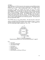
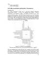
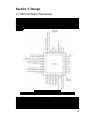
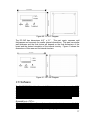
Section 11. Appendix C – Permissions
I. Enpirion EP5368QI Permission
RE: Permission to reprint images for School Project
Karen Boyle <[email protected]>
To: "[email protected]" <[email protected]>
Mon, Dec 7, 2009 at 2:00 PM
Hello Mr. Roberts,
You may use the figure on the data sheet. Good luck!
Karen
Karen Boyle
Enpirion, Inc.
Perryville III
53 Frontage Road, Suite 210
Hampton, NJ 08827
Phone: 908.894.6017
-----Original Message----From: Margaret Nolin
Sent: Friday, December 04, 2009 8:07 PM
To: Karen Boyle
Subject: FW: Permission to reprint images for School Project
I think this customer is in Florida.
Margaret
-----Original Message----From: [email protected] [mailto:[email protected]] On Behalf Of Eric Roberts
Sent: Friday, December 04, 2009 3:08 PM
To: Margaret Nolin
Subject: Permission to reprint images for School Project
Hello,
My senior design group is designing a wireless pulse oximeter and we are considering the
use of the Enpirion EP5368QI buck converter for our device. As part of the design processes
we are required to submit a document with all of our designs and figures. Can we use the
figure in the EP5368QI data sheet that shows the typical application of the EP5368QI?
-Thank you,
Eric Roberts
IV
II. Texas Instruments 2009 Permission:
IMPORTANT NOTICE
Texas Instruments Incorporated and its subsidiaries (TI) reserve the right to make corrections, modifications, enhancements,
improvements, and other changes to its products and services at any time and to discontinue any product or service without
notice. Customers should obtain the latest relevant information before placing orders and should verify that such information is
current and complete. All products are sold subject to TI’s terms and conditions of sale supplied at the time of order
acknowledgment.
TI warrants performance of its hardware products to the specifications applicable at the time of sale in accordance with TI’s
standard warranty. Testing and other quality control techniques are used to the extent TI deems necessary to support this
warranty. Except where mandated by government requirements, testing of all parameters of each product is not necessarily
performed.
TI assumes no liability for applications assistance or customer product design. Customers are responsible for their products and
applications using TI components. To minimize the risks associated with customer products and applications, customers should
provide adequate design and operating safeguards.
TI does not warrant or represent that any license, either express or implied, is granted under any TI patent right, copyright, mask
work right, or other TI intellectual property right relating to any combination, machine, or process in which TI products or services
are used. Information published by TI regarding third-party products or services does not constitute a license from TI to use such
products or services or a warranty or endorsement thereof. Use of such information may require a license from a third party under
the patents or other intellectual property of the third party, or a license from TI under the patents or other intellectual property of TI.
Reproduction of TI information in TI data books or data sheets is permissible only if reproduction is without alteration and is
accompanied by all associated warranties, conditions, limitations, and notices. Reproduction of this information with alteration is
an unfair and deceptive business practice. TI is not responsible or liable for such altered documentation. Information of third
parties may be subject to additional restrictions.
Resale of TI products or services with statements different from or beyond the parameters stated by TI for that product or service
voids all express and any implied warranties for the associated TI product or service and is an unfair and deceptive business
practice. TI is not responsible or liable for any such statements.
TI products are not authorized for use in safety-critical applications (such as life support) where a failure of the TI product would
reasonably be expected to cause severe personal injury or death, unless officers of the parties have executed an agreement
specifically governing such use. Buyers represent that they have all necessary expertise in the safety and regulatory ramifications
of their applications, and acknowledge and agree that they are solely responsible for all legal, regulatory and safety-related
requirements concerning their products and any use of TI products in such safety-critical applications, notwithstanding any
applications-related information or support that may be provided by TI. Further, Buyers must fully indemnify TI and its
representatives against any damages arising out of the use of TI products in such safety-critical applications.
TI products are neither designed nor intended for use in military/aerospace applications or environments unless the TI products
are specifically designated by TI as military-grade or "enhanced plastic." Only products designated by TI as military-grade meet
military specifications. Buyers acknowledge and agree that any such use of TI products which TI has not designated as militarygrade is solely at the Buyer's risk, and that they are solely responsible for compliance with all legal and regulatory requirements in
connection with such use.
TI products are neither designed nor intended for use in automotive applications or environments unless the specific TI products
are designated by TI as compliant with ISO/TS 16949 requirements. Buyers acknowledge and agree that, if they use any nondesignated products in automotive applications, TI will not be responsible for any failure to meet such requirements.
Following are URLs where you can obtain information on other Texas Instruments products and application solutions:
Products
Amplifiers
Data Converters
DLP® Products
DSP
Clocks and Timers
Interface
Logic
Power Mgmt
Microcontrollers
RFID
RF/IF and ZigBee® Solutions
amplifier.ti.com
dataconverter.ti.com
www.dlp.com
dsp.ti.com
www.ti.com/clocks
interface.ti.com
logic.ti.com
power.ti.com
microcontroller.ti.com
www.ti-rfid.com
www.ti.com/lprf
Applications
Audio
Automotive
Broadband
Digital Control
Medical
Military
Optical Networking
Security
Telephony
Video & Imaging
Wireless
www.ti.com/audio
www.ti.com/automotive
www.ti.com/broadband
www.ti.com/digitalcontrol
www.ti.com/medical
www.ti.com/military
www.ti.com/opticalnetwork
www.ti.com/security
www.ti.com/telephony
www.ti.com/video
www.ti.com/wireless
Mailing Address: Texas Instruments, Post Office Box 655303, Dallas, Texas 75265
Copyright © 2009, Texas Instruments Incorporated
V
III. Texas Instruments 2008 Permission:
IMPORTANT NOTICE
Texas Instruments Incorporated and its subsidiaries (TI) reserve the right to make corrections, modifications, enhancements,
improvements, and other changes to its products and services at any time and to discontinue any product or service without
notice. Customers should obtain the latest relevant information before placing orders and should verify that such information is
current and complete. All products are sold subject to TI’s terms and conditions of sale supplied at the time of order
acknowledgment.
TI warrants performance of its hardware products to the specifications applicable at the time of sale in accordance with TI’s
standard warranty. Testing and other quality control techniques are used to the extent TI deems necessary to support this
warranty. Except where mandated by government requirements, testing of all parameters of each product is not necessarily
performed.
TI assumes no liability for applications assistance or customer product design. Customers are responsible for their products and
applications using TI components. To minimize the risks associated with customer products and applications, customers should
provide adequate design and operating safeguards.
TI does not warrant or represent that any license, either express or implied, is granted under any TI patent right, copyright, mask
work right, or other TI intellectual property right relating to any combination, machine, or process in which TI products or services
are used. Information published by TI regarding third-party products or services does not constitute a license from TI to use such
products or services or a warranty or endorsement thereof. Use of such information may require a license from a third party under
the patents or other intellectual property of the third party, or a license from TI under the patents or other intellectual property of TI.
Reproduction of TI information in TI data books or data sheets is permissible only if reproduction is without alteration and is
accompanied by all associated warranties, conditions, limitations, and notices. Reproduction of this information with alteration is
an unfair and deceptive business practice. TI is not responsible or liable for such altered documentation. Information of third
parties may be subject to additional restrictions.
Resale of TI products or services with statements different from or beyond the parameters stated by TI for that product or service
voids all express and any implied warranties for the associated TI product or service and is an unfair and deceptive business
practice. TI is not responsible or liable for any such statements.
TI products are not authorized for use in safety-critical applications (such as life support) where a failure of the TI product would
reasonably be expected to cause severe personal injury or death, unless officers of the parties have executed an agreement
specifically governing such use. Buyers represent that they have all necessary expertise in the safety and regulatory ramifications
of their applications, and acknowledge and agree that they are solely responsible for all legal, regulatory and safety-related
requirements concerning their products and any use of TI products in such safety-critical applications, notwithstanding any
applications-related information or support that may be provided by TI. Further, Buyers must fully indemnify TI and its
representatives against any damages arising out of the use of TI products in such safety-critical applications.
TI products are neither designed nor intended for use in military/aerospace applications or environments unless the TI products
are specifically designated by TI as military-grade or "enhanced plastic." Only products designated by TI as military-grade meet
military specifications. Buyers acknowledge and agree that any such use of TI products which TI has not designated as militarygrade is solely at the Buyer's risk, and that they are solely responsible for compliance with all legal and regulatory requirements in
connection with such use.
TI products are neither designed nor intended for use in automotive applications or environments unless the specific TI products
are designated by TI as compliant with ISO/TS 16949 requirements. Buyers acknowledge and agree that, if they use any nondesignated products in automotive applications, TI will not be responsible for any failure to meet such requirements.
Following are URLs where you can obtain information on other Texas Instruments products and application solutions:
Products
Amplifiers
Data Converters
DSP
Clocks and Timers
Interface
Logic
Power Mgmt
Microcontrollers
RFID
RF/IF and ZigBee® Solutions
amplifier.ti.com
dataconverter.ti.com
dsp.ti.com
www.ti.com/clocks
interface.ti.com
logic.ti.com
power.ti.com
microcontroller.ti.com
www.ti-rfid.com
www.ti.com/lprf
Applications
Audio
Automotive
Broadband
Digital Control
Medical
Military
Optical Networking
Security
Telephony
Video & Imaging
Wireless
www.ti.com/audio
www.ti.com/automotive
www.ti.com/broadband
www.ti.com/digitalcontrol
www.ti.com/medical
www.ti.com/military
www.ti.com/opticalnetwork
www.ti.com/security
www.ti.com/telephony
www.ti.com/video
www.ti.com/wireless
Mailing Address: Texas Instruments, Post Office Box 655303, Dallas, Texas 75265
Copyright © 2008, Texas Instruments Incorporated
VI
IV. Saft LS14500 Battery Permission:
RE: SaftBatteries.com - Permission to
use Images
Fri, Dec 4, 2009
at 8:11 AM
White,Jennifer <[email protected]>
To: [email protected]
Eric,
Yes, this is fine.
Best Regards,
Jennifer
Jennifer White
Business Development Specialist
Saft America, Inc.
(828) 879-5096 Phone
(828) 443-0236 Cell
(828) 879-3981 Fax
------------------------------------------From: [email protected][SMTP:[email protected]]
Sent: Saturday, November 28, 2009 8:00:48 PM
To: lithium sales
Subject: SaftBatteries.com - Permission to use Images
Home > Contacts > North America > USA >
Mr Eric Roberts
Company : Student of University of Central Florida
Mail : mailto:[email protected]@knights.ucf.edu
Telephone :
Hello, My senior design group is designing a wireless pulse oximeter and we
are considering the use of the Saft LS14500 batteries to power our devices.
As part of the design processes we are required to submit a document with all
of our design sand figures. Can we use the figure in the LS14500 data sheet
that displays the dimensions of the LS14500? Thank you, Eric Roberts
VII
V. ON Semiconductor NCP1530 Permission
VIII