1
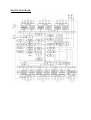
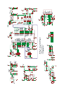
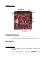
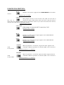
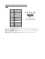
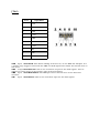
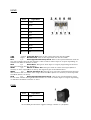
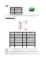
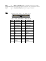
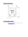
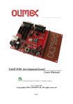
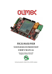
AVR-TLCD-128CAN development board
Users Manual
Rev.A, July 2008
Copyright(c) 2008, OLIMEX Ltd, All rights reserved
INTRODUCTION:
AVR-TLCD-128CAN adds cool LCD and touchscreen interface to your next
project. There is AT90CAN128 on board with all microcontroller pins
available for plug-in additional boards
BOARD FEATURES:
−
−
−
−
−
−
−
−
−
−
−
−
−
MCU: AT90CAN128 128KB Flash memory, 4096B RAM, 4096B
EEPROM
TOUCH SCREEN LCD 160x160 dots B/W 81x60 mm view area
Stainless steel front panel (102x85 mm 4x3.35'') with easy to mount x4
3 mm fixing screws
JTAG connector for programming and debugging with AVR-JTAG-L or
AVR-JTAG-USB
ICSP connector for programming with AVR-PG1 or AVR-GP2
SD/MMC card connector
CAN driver and connector
UEXT connector for connection to other Olimex modules like MOD-MP3,
MOD-NRF24Lx, MOD-GPS and many others
8 MHz crystal
Extension connectors for all AT90CAN128 ports
+(4.5–6.0) battery connector
PCB: FR-4, 1.5 mm (0,062''), soldermask, silkscreen component print
Dimensions 102x85 mm (4 x 3.35")
ELECTROSTATIC WARNING:
The AVR-TLCD-128CAN board is shipped in protective anti-static
packaging. The board must not be subject to high electrostatic potentials.
General practice for working with static sensitive devices should be applied
when working with this board.
BOARD USE REQUIREMENTS:
Cables:
1.8 meter USB A-B cable to connect AVR-JTAG-USB to USB
host on PC. If you use AVR-JTAG(-L) or AVR-PG1, you will
need RS232 cable. If you use AVR-PG2 you will need LPC
cable. Other cables might be required in case of other
programming/debugging tools.
Hardware:
Programmer/Debugger – AVR-JTAG(-L), AVR-JTAG-USB,
AVR-PG1, AVR-PG2 or other compatible
programming/debugging tool.
Software:
AVR Studio 4.13 (or later) + WinAVR (latest version) or IAR
AVR. AVR Studio and WinAVR are free to download and use.
Take a note that AVR Studio 4.13 has a bug and doesn't read
the fuses correctly. On our request to Atmel support they had
confirmed the bug and had suggested to fix the bug by “AVR
Studio
4.13
SP2
JTAGICE
Fix”
available
from
http://www.atmel.no/beta_ware/. For programming with
AVR-PG1 you could use PonyProg and for programming with
AVR-PG2 you could use PonyProg, AVR Dude or other
compatible tools.
PROCESSOR FEATURES:
AVR-TLCD-128CAN board use MCU AT90CAN128 from Atmel with these
features:
High-performance, Low-power AVR® 8-bit Microcontroller
Advanced RISC Architecture
- 133 Powerful Instructions – Most Single Clock Cycle Execution
- 32 x 8 General Purpose Working Registers + Peripheral Control
Registers
- Fully Static Operation
- Up to 16 MIPS Throughput at 16 MHz
- On-chip 2-cycle Multiplier
Non volatile Program and Data Memories
- 128K Bytes of In-System Reprogrammable Flash
o Endurance: 10,000 Write/Erase Cycles
- Optional Boot Code Section with Independent Lock Bits
o Selectable Boot Size: 1K Bytes, 2K Bytes, 4K Bytes or 8K
Bytes
o In-System Programming by On-Chip Boot Program (CAN,
UART, ...)
o True Read-While-Write Operation
- 4K Bytes EEPROM (Endurance: 100,000 Write/Erase Cycles)
- 4K Bytes Internal SRAM (AT90CAN32/64/128)
- Up to 64K Bytes Optional External Memory Space
- Programming Lock for Software Security
JTAG (IEEE std. 1149.1 Compliant) Interface
- Boundary-scan Capabilities According to the JTAG Standard
- Programming Flash (Hardware ISP), EEPROM, Lock & Fuse Bits
- Extensive On-chip Debug Support
CAN Controller 2.0A & 2.0B - ISO 16845 Certified
- 15 Full Message Objects with Separate Identifier Tags and Masks
- Transmit, Receive, Automatic Reply and Frame Buffer Receive
Modes
- 1Mbits/s Maximum Transfer Rate at 8 MHz
- Time stamping, TTC & Listening Mode (Spying or Autobaud)
Peripheral Features
- Programmable Watchdog Timer with On-chip Oscillator
- 8-bit Synchronous Timer/Counter-0
o 10-bit Prescaler
o External Event Counter
o Output Compare or 8-bit PWM Output
- 8-bit Asynchronous Timer/Counter-2
o 10-bit Prescaler
o External Event Counter
o Output Compare or 8-Bit PWM Output
o 32Khz Oscillator for RTC Operation
- Dual 16-bit Synchronous Timer/Counters-1 & 3
o 10-bit Prescaler
o Input Capture with Noise Canceler
o External Event Counter
o 3-Output Compare or 16-Bit PWM Output
o Output Compare Modulation
- 8-channel, 10-bit SAR ADC
o 8 Single-ended Channels
o 7 Differential Channels
2 Differential Channels With Programmable Gain at 1x,
10x, or 200x
- On-chip Analog Comparator
- Byte-oriented Two-wire Serial Interface
- Dual Programmable Serial USART
- Master/Slave SPI Serial Interface
o Programming Flash (Hardware ISP)
Special Microcontroller Features
- Power-on Reset and Programmable Brown-out Detection
- Internal Calibrated RC Oscillator
- 8 External Interrupt Sources
- 5 Sleep Modes: Idle, ADC Noise Reduction, Power-save, Power-down
& Standby
- Software Selectable Clock Frequency
- Global Pull-up Disable
I/O and Packages
- 53 Programmable I/O Lines
- 64-lead TQFP and 64-lead QFN
Operating Voltages: 2.7 - 5.5V
Operating temperature: Industrial (-40°C to +85°C)
Maximum Frequency: 8 MHz at 2.7V, 16 MHz at 4.5V
o
BLOCK DIAGRAM:
MEMORY MAP:
SCHEMATIC:
BOARD LAYOUT:
POWER SUPPLY CIRCUIT:
AVR-TLCD-128CAN should be powered by 4.5VAC or +(6-9VDC).
The board power consumption at 8 VDC the consumption is about 20 mA.
RESET CIRCUIT:
AVR-TLCD-128CAN reset circuit is realized with MCP130T which on power
failure or if you apply low level at EXT-3 resets the MCU.
CLOCK CIRCUIT:
Quartz crystal 8 MHz is connected to AT90CAN128 pin 24 (XTAL1) and pin
23 (XTAL2).
Quartz crystal 32.768 kHz is connected to AT90CAN128 pin 19
(TOSC1/PG4) and pin 18 (TOSC2/PG3) and supplies the internal
Asynchronous
Timer/Counter
(Timer/Counter2
in
asynchronous
operation).
JUMPER DESCRIPTION:
18V_E
Enables 18 V power supply for the AT90CAN128 and all other
devices.
Default state is closed.
CAN_T
This jumper assures correct work of the CAN. At each end of
the bus it
should be closed. This means that if you have only two devices
with CAN, the jumpers of both devices should be closed. If you have more than two devices,
only the two end-devices should be closed.
Default state is closed.
CAN_CTRL
If this jumper is closed the MCU controls the CAN.
Default state is closed.
WP_E
Enables the Write Protect input signal to the AT90CAN128.
Default state is closed.
CP_E
Enables the Card Present input signal to the AT90CAN128.
Default state is closed.
TD1/PD5
When in position 1-2 shorted, outputs the TD1 signal to the
controller. When in position 2-3 shorted, EXT-12 is connected
CAN
to TD1/PD5.
Default position is 1-2 shorted.
RD1/PD6
CAN
to RD1/PD6.
When in position 1-2 shorted, inputs the RD1 signal from the
controller. When in position 2-3 shorted, EXT-13 is connected
Default position is 1-2 shorted.
INPUT/OUTPUT:
Power-on red LED with name PWR_LED connected to EXT-1 and EXT-2.
Accelerometer SMB380.
Touchscreen LCD PC0919WE07.
EXTERNAL CONNECTORS DESCRIPTION:
ICSP:
Pin #
Signal Name
1
PDI
2
+3.3V
3
NC
4
GND
5
RESET
6
GND
7
SCK
8
GND
9
PDO
10
GND
PDI
Input Programming Data In. This pin is used for data input while programming
the MCU through ICSP.
PDO OutputProgramming Data Out. This pin is used for daa output while programming
the MCU through ICSP.
SCK Input Serial (Synchronization) Clock. This pin is input for the MCU while
programming.
JTAG:
Pin #
Signal Name
1
TCK
2
GND
3
TDO
4
+3.3V
5
TMS
6
RESET
7
+3.3V
8
NC
9
TDI
10
GND
TCK Input Test Clock. This allows shifting of the data in, on the TMS and TDI pins. It is
a positive edge triggered clock with the TMS and TCK signals that define the internal state of
the device.
TDO OutputTest Data Out. This is the serial data output for the shift register. Data is
shifted out of the device on he negative edge of the TCK signal.
TMS Input Test Mode Select. The TMS pin selects the next state in the TAP state
machine.
TDI
Input Test Data In. This is the serial data input for the shift register.
UEXT:
Pin #
Signal Name
1
+3.3V
2
GND
3
TXD
4
RXD
5
SCL
6
SDA
7
MISO
8
MOSI
9
SCK
10
SS
TXD
Output Transmit Data. This is the output data line for the UART.
RXD
Input
Receive Data. This is the input data line for the UART.
SCL
I/O
Serial (Synchronization) Clock. This is the synchronization clock for
the data transfer through I2C interface. This could be either input or output depending on
whether the MCU is master or slave.
SDA
I/O
Serial Data. This pin is data input or output (depending on the data
flow direction) for the I2C interface.
MISO
I/O
Master In Slave Out. This pin could be either data input (MCU is
master) or data output(MCU is slave). The signal is pat of the SPI interface.
MOSI
I/O
Master Out Slave In. This pin is be used for communication through
SPI interface and it is either data output from the MCU (when it is master) or data input for
the MCU (when it is slave).
SCK
I/O
Serial (Synchronization) Clock . This is the synchronization clock
for the data transfer through the SPI interface. It could be either input or output depending
on whether the MCU is master or slave.
PWR:
Pin #
Signal Name
1
PWR
2
GND
At the PWR pin should be applied voltage 4.5VAC or +(6-9)VDC.
CAN:
Pin #
Signal Name
1
GND
2
CANL
3
CANH
CANL and CANH are either deferential input, or differential output depending
on the function of the SN65FVD230 CAN controller (receiving or transmitting data).
SD/MMC card slot:
Pin #
Signal Name
Pin #
Signal Name
1
CS_SD
2
MOSI
3
GND
4
VDD (+3.3V)
5
SCK
6
GND
7
MISO
8
+3.3V
9
+3.3V
10
WP_E
11
-
12
-
13
CP_E
14
GND
15
GND
CS_SD
Output
SD/MMC.
MOSI
Output
interface, this is data
card (which is slave).
SCK
Output
the data transfer.
Chip Select SD. The signal on this pin enables or disables the
Master Out Slave In. As the access to the memory is via SPI
output from the MCU (which is master) and input for the memory
Serial (Synchronization) Clock. This is the synchronization clock for
MISO
I/O
interface, this is data
card (which is slave).
WP_E
Input
CP_E
Input
Master In Slave Out. As the access to the memory card is via SPI
input for the MCU(which is master) and data output from the memory
Write Protect Enable. This signal is input for the MCU.
Card Present Enable. This signal is input for the MCU.
EXT:
Pin #
Signal Name
Pin #
Signal Name
1
+3.3V
2
GND
3
RESET
4
XCK0/AIN0/PE2
5
OC3A/AIN1/PE3
6
OC3B/INT4/PE4
7
OC3C/INT5/PE5
8
IC3/INT7/PE7
9
SCL
10
SDA
11
IC1/PD4
12
PD5
13
PD6
14
T2/PD7/T0
15
WP
16
CP
17
CS_SD
18
PB4/OC0
19
PB5/OC1A
20
PB6/OC1B
21
PC5/A13
22
PC4/A12
23
PC3/A11
24
PC2/A10
25
PC1/A9
26
PC0/A8
MECHANICAL DIMENSIONS:
All measures are in mm
AVAILABLE DEMO SOFTWARE:
You could find information about AVR-TLCD-128CAN demo software at
www.olimex.com/dev.
ORDER CODE:
AVR-TLCD-128CAN – assembled and tested (no kit, no soldering required)
How to order?
You can order to us directly or by any of our distributors.
Check our web www.olimex.com/dev for more info.
All boards produced by Olimex are RoHS compliant
Revision history:
REV.A
- created
July 2008
Disclaimer:
© 2008 Olimex Ltd. All rights reserved. Olimex®, logo and combinations thereof, are
registered trademarks of Olimex Ltd. Other terms and product names may be trademarks of
others.
The information in this document is provided in connection with Olimex products. No
license, express or implied or otherwise, to any intellectual property right is granted by this
document or in connection with the sale of Olimex products.
Neither the whole nor any part of the information contained in or the product described in
this document may be adapted or reproduced in any material from except with the prior
written permission of the copyright holder.
The product described in this document is subject to continuous development and
improvements. All particulars of the product and its use contained in this document are
given by OLIMEX in good faith. However all warranties implied or expressed including but
not limited to implied warranties of merchantability or fitness for purpose are excluded.
This document is intended only to assist the reader in the use of the product. OLIMEX Ltd.
shall not be liable for any loss or damage arising from the use of any information in this
document or any error or omission in such information or any incorrect use of the product.