1
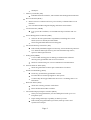
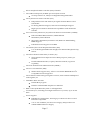
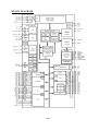
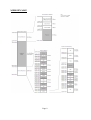
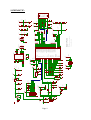
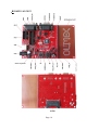
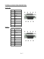
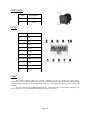
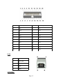
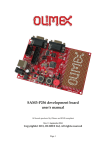
SAM7-P256 development board Users Manual All boards produced by Olimex are ROHS compliant Rev. F, August 2008 Copyright(c) 2010, OLIMEX Ltd, All rights reserved Page 1 INTRODUCTION: Atmel’s AT91SAM7S256 is a member of a series of low pincount Flash microcontrollers based on the 32-bit ARM RISC processor. It features a 256 Kbyte high-speed Flash and a 64 Kbyte SRAM, a large set of peripherals, including a USB 2.0 device, and a complete set of system functions minimizing the number of external components. The device is an ideal migration path for 8-bit microcontroller users looking for additional performance and extended memory. The embedded Flash memory can be programmed in-system via the JTAGICE interface or via a parallel interface on a production programmer prior to mounting. Built-in lock bits and a security bit protect the firmware from accidental overwrite and preserves its confidentiality. The AT91SAM7S256 system controller includes a reset controller capable of managing the power-on sequence of the microcontroller and the complete system. Correct device operation can be monitored by a built-in brownout detector and a watchdog running off an integrated RC oscillator. The AT91SAM7S256 is a general-purpose microcontroller. Its integrated USB Device port makes it an ideal device for peripheral applications requiring connectivity to a PC or cellular phone. Its aggressive price point and high level of integration pushes its scope of use far into the cost-sensitive, high-volume consumer market. BOARD FEATURES: • Microcontroller: AT91SAM7S256 16/32 bit ARM7TDMI™ with 256K Bytes Program Flash, 64K Bytes RAM, USB 2.0, RTT, 10 bit ADC 384 ksps, 2x UARTs, TWI (I2C), SPI, 3x 32bit TIMERS, 4x PWM, SSC, WDT, PDC (DMA) for all peripherals, up to 60MHz operation • standard JTAG connector with ARM 2x10 pin layout for programming/debugging with ARM-JTAG • USB connector • Two channel RS232 interface and drivers • SD/MMC card connector • two buttons • trimpot connected to ADC • thermistor connected to ADC • two status LEDs • on board voltage regulator 3.3V with up to 800mA current • single power supply: 6V AC or DC required • power supply LED • power supply filtering capacitor • RESET circuit • RESET button Page 2 • 18.432 Mhz crystal on socket • extension headers for all microcontroller's ports • PCB: FR-4, 1.5 mm (0,062"), soldermask, silkscreen component print • Dimensions: 120 x 80 mm (4.7 x 3.15") ELECTROSTATIC WARNING: The SAM7-P256 board is shipped in protective anti-static packaging. The board must not be subject to high electrostatic potentials. General practice for working with static sensitive devices should be applied when working with this board. BOARD USE REQUIREMENTS: Cables: The cable you will need depends on the programmer/debugger you use. If you use ARM-JTAG-EW, you will need USB A-B cable. Hardware: Programmer/Debugger ARM-JTAG-EW or other compatible programming/debugging tool if you work with EW-ARM. You can use also ARM-USB-OCD, ARM-USB-TINY, ARM-USB-TINY-H . PROCESSOR FEATURES: SAM7-P256 board use AT91 ARM Thumb-based microcontroller AT91SAM7S256 from Atmel Corporation with these features: − High-performance 32-bit RISC Architecture − High-density 16-bit Instruction Set − Leader in MIPS/Watt − EmbeddedICE™ In-circuit Emulation, Debug Communication Channel Support − Internal High-speed Flash − − 256 Kbytes Organized in 1024 Pages of 256 Bytes (Single Plane) − Single Cycle Access at Up to 30 MHz in Worst Case Conditions − Prefetch Buffer Optimizing Thumb Instruction Execution at Maximum Speed − Page Programming Time: 6 ms, Including Page Auto-erase, Full Erase Time: 15 ms − 10,000 Write Cycles, 10-year Data Retention Capability, Sector Lock Capabilities, Flash Security Bit − Fast Flash Programming Interface for High Volume Production Internal High-speed SRAM, Single-cycle Access at Maximum Speed Page 3 − − Memory Controller (MC) − − − − − − − Based on Power-on Reset and Low-power Factory-calibrated Brown-out Detector − Provides External Reset Signal Shaping and Reset Source Status Clock Generator (CKGR) − − Low-power RC Oscillator, 3 to 20 MHz On-chip Oscillator and one PLL Power Management Controller (PMC) − Software Power Optimization Capabilities, Including Slow Clock Mode (Down to 500 Hz) and Idle Mode − Three Programmable External Clock Signals Advanced Interrupt Controller (AIC) − Individually Maskable, Eight-level Priority, Vectored Interrupt Sources − Two External Interrupt Source(s) and One Fast Interrupt Source, Spurious Interrupt Protected Debug Unit (DBGU) − 2-wire UART and Support for Debug Communication Channel interrupt, Programmable ICE Access Prevention − Mode for General Purpose 2-wire UART Serial Communication Periodic Interval Timer (PIT) − − Embedded Flash Controller, Abort Status and Misalignment Detection Reset Controller (RSTC) − − 64 Kbytes 20-bit Programmable Counter plus 12-bit Interval Counter Windowed Watchdog (WDT) − 12-bit key-protected Programmable Counter − Provides Reset or Interrupt Signals to the System − Counter May Be Stopped While the Processor is in Debug State or in Idle Mode Real-time Timer (RTT) − 32-bit Free-running Counter with Alarm − Runs Off the Internal RC Oscillator One Parallel Input/Output Controller (PIOA) − Thirty-two Programmable I/O Lines Multiplexed with up to Two Peripheral I/Os − Input Change Interrupt Capability on Each I/O Line − Individually Programmable Open-drain, Pull-up resistor and Synchronous Output Page 4 − Eleven Peripheral DMA Controller (PDC) Channels − One USB 2.0 Full Speed (12 Mbits per Second) Device Port − − − − One Synchronous Serial Controller (SSC) − Independent Clock and Frame Sync Signals for Each Receiver and Transmitter − I2S Analog Interface Support, Time Division Multiplex Support − High-speed Continuous Data Stream Capabilities with 32-bit Data Transfer Two Universal Synchronous/Asynchronous Receiver Transmitters (USART) − Individual Baud Rate Generator, IrDA® Infrared Modulation/Demodulation − Support for ISO7816 T0/T1 Smart Card, Hardware Handshaking, RS485 Support − Full Modem Line Support on USART1 One Master/Slave Serial Peripheral Interface (SPI) − − On-chip Transceiver, 328-byte Configurable Integrated FIFOs 8- to 16-bit Programmable Data Length, Four External Peripheral Chip Selects One Three-channel 16-bit Timer/Counter (TC) − Three External Clock Input and Two Multi-purpose I/O Pins per Channel − Double PWM Generation, Capture/Waveform Mode, Up/Down Capability − One Four-channel 16-bit PWM Controller (PWMC) − One Two-wire Interface (TWI) − Master Mode Support Only, All Two-wire Atmel EEPROMs and I2C Compatible Devices Supported − One 8-channel 10-bit Analog-to-Digital Converter, Four Channels Multiplexed with Digital I/Os − SAM-BA™ Boot Assistant − Default Boot program − Interface with SAM-BA Graphic User Interface − IEEE® 1149.1 JTAG Boundary Scan on All Digital Pins − 5V-tolerant I/Os, including Four High-current Drive I/O lines, Up to 16 mA Each − Power Supplies − Embedded 1.8V Regulator, Drawing up to 100 mA for the Core and External Components − 3.3V or 1.8V VDDIO I/O Lines Power Supply, Independent 3.3V VDDFLASH Flash Power Supply Page 5 − − 1.8V VDDCORE Core Power Supply with Brown-out Detector Fully Static Operation: Up to 55 MHz at 1.65V and 85ーC Worst Case Condition Page 6 BLOCK DIAGRAM: Page 7 MEMORY MAP: Page 8 Page 9 USB S H IE LD 1 2 3 4 USB G ND 10n C32 100n C12 C2 15p 100 R34 330K DP_PUP R12 47K 3.3V R16 R32 330K FET1 IRLML6402 27 R36 27 DM_PUP 1nF C26 15p C1 TDO TDI TMS TCK R18 47K 10nF C29 R9 1.5K R21 390/1% 2 VCC 1n C23 C22 100n C15 100n C25 2.2uF R7 560 R47 4.7K 3.3V 100n C9 C21 100n C10 100n TXD1 TWCK MISO SPCK R45 R44 C28 10p C27 10p 1 3 5 7 9 100n 12 9 330 330 RST UEXT 2 4 6 8 10 100n C4 RXD1 TWD MOSI NPCS1 2 17 46 60 12 24 54 64 8 18 45 58 59 7 62 63 56 57 50 53 33 49 51 40 39 55 R37 NA Q1 61 18.432MHz TCK TDI TDO TMS 2 1 GND1 GND2 GND3 GND4 VDDCORE1 VDDCORE2 VDDCORE3 VDDPLL VDDOUT VDDIO1 VDDIO2 VDDIO3 VDDFLASH VDDIN XOUT XIN PLLRC DDM DDP JTAGSEL TCK TDI TDO TMS TST NRST ERASE U1 C20 100n GND15 R1IN R2IN T1OUT T2OUT V- V+ U2 MAX3232 U2PWR 16VCC R1OUT R2OUT T1IN T2IN C2- C2+ C1- C1+ R46 4.7K 3.3V AT91SAM7S256 3.3V 11 10 5 T0IN TXD1 C17 100n 4 3 C16 1 100n 3.3V 3.3V TEST 3.3V C7 3.3V 100n C6 RST BDS 2 1 R0OUT RXD1 RST 3.3V 3.3V NA C8 RST R8 10K 2.2uF C30 RESET C24 100n GND RESET 1 U5 MCP130T 47uF/6.3V C13 PWR_LED 3.3V C19 100n C18 100n 1 2 3 4 5 ADVREF AD4 AD5 AD6 AD7 PA0/PWM0/TIOA0 PA1/PWM1/TIOB0 PA2/PWM2/SCK0 PA3/TWD/NPCS3 PA4/TWCK/TCLK0 PA5/RXD0/NPCS3 PA6/TXD0/PCK0 PA7/RTS0/PWM3 PA8/CTS0/ADTRG PA9/DRXD/NPCS1 PA10/DTXD/NPCS2 PA11/NPCS0/PWM0 PA12/MISO/PWM1 PA13/MOSI/PWM2 PA14/SPCK/PWM3 PA15/TF/TIOA1 PA16/TK/TIOB1 PA17/TD/PCK1/AD0 PA18/RD/PCK2/AD1 PA19/RK/FIQ/AD2 PA20/RF/IRQ0/AD3 PA21/RXD1/PCK1 PA22/TXD1/NPCS3 PA23/SCK1/PWM0 PA24/RTS1/PWM1 PA25/CTS1/PWM2 PA26/DCD1/TIOA2 PA27/DTR1/TIOB2 PA28/DSR1/TCLK1 PA29/RI1/TCLK2 PA30/IRQ1/NPCS2 PA31/NPCS1/PCK2 13 RX0IN RX1IN 8 14 TX0OUT 7 TX1OUT 6 2 AD6 AD7 NPCS1 USB_D WP NPCS0 MISO MOSI SPCK CP DP_PUP LED2 LED1 B1 B2 RXD1 TXD1 DM_PUP TWD TWCK P A 25 P A 26 P A 27 P A 28 P A 29 P A 30 P A 31 P A 23 http://www.olimex.com/dev 2 1 PA11 PA12 PA13 PA14 100n 3.3V CP 3.3V T0IN R0OUT TXD0/DTXD AD4 R26 0 MISO R22 33K R30 R31 R33 0 3.3V R24 2K 47K 47K R17 10K AD5 13 15 1 2 3 4 5 6 7 8 9 10 14 SD-CARD CP1 CP2 CD/DAT3/CS CMD/DI VSS1 VDD CLK/SCLK VSS2 DAT0/DO DAT1/RES DAT2/RES WP1 WP2 SD/MMC 47uF/6.3V C31 470nH R42 330 B2 R14 10K 3.3V R43 33K 3.3V B2 TH1 TERMISTOR 3.3V 3.3V 3.3V L1 SPCK NPCS0 MOSI 2k R23 33K R41 330 B1 R13 10K 3.3V 3.3V B1 R19 AN_TR 10K 3.3V 0 R27 R28 47K PA9 PA10 PA5 PA6 WP LED2 LED2 R29 560 R25 560 LED1 YELLO W 2 1 3.3V G REEN 3.3V LED1 VREF_P VREF C14 NPCS0 MISO MOSI SPCK COPYRIGHT(C) 2008, O LIMEX Ltd. Rev. F 6 7 8 9 RS232_1 RXD0/DRXD P A 15 PA7 PA8 PA0 PA1 PA2 PA3 PA4 TX1OUT RX1IN 1 2 3 4 5 SAM7-P256 1 3 4 5 6 48 47 44 43 36 35 34 32 31 30 29 28 27 22 21 20 19 9 10 13 16 11 14 15 23 25 26 37 38 41 42 52 6 7 8 9 RS232_0/D 2 1 1.5K R15 33p C3 R35 100 R40 R38 47K RST R1 47K NA C11 R20 240/1% 3 USB_SHIELD R11 22K 1.5K 0 R2 47K 3.3V 0 R6 R3 47K R5 FET3 IRLML6402 RTCK TRST R4 47K 470uF/16VDC C5 ADJ/GND 3.3V 3 2 1 15K R10 1 3 5 7 9 11 13 15 17 19 + R39 JTAG 3.3V D1 1N5819 + 3 2 1 USB_D +5V 2 4 6 8 10 12 14 16 18 20 G1 B-DIL OUT + + 5V _US B 6VDC 4.5VAC PWR IN VR1(3.3V) LM1117 SCHEMATIC: + BOARD LAYOUT: Page 10 POWER SUPPLY CIRCUIT: SAM7-P256 is typically power supplied with 6 VDC. The programmed board power consumption is about 30 mA. RESET CIRCUIT: SAM7-P256 reset circuit includes U5 (MCP130T), R8 (10k), pin 15 of JTAG connector, pin 39 (NRST) of AT91SAM7S256 and RESET button. CLOCK CIRCUIT: Quartz crystal Q1 18.432 MHz is connected to AT91SAM7S256 pin 61 (XOUT) and pin 62 (XIN). JUMPER DESCRIPTION: Page 11 Description for programming via RS232_0/D COM port, when is SAMBA software The AT91SAM7S256 can be programmed via COM port using the SAM-BATM software. Before being able to use SAM-BA, a recovery procedure, which consists of copying the SAM-BA Boot Assistant into Flash must be performed as follows: 1. Power down the AT91SAM7S256 2. Close jumper TST 3. Power up the AT91SAM7S256 4. Wait 10 sec 5. Power down the AT91SAM7S256 6. Remove jumper TST 7. Power up the AT91SAM7S256 Note: For programming via COM port, you must set jumpers RXD0/DRXD and TXD0/DTXD, according to jumpers description above. INPUT/OUTPUT: Status Led (green) with name GREEN connected via jumper LED1 to AT91SAM7S256 pin 10 (PA18/RD/PCK2/AD1). Status Led (yellow) with name YELLOW connected via jumper LED2 to AT91SAM7S256 pin 9 (PPA17/TD/PCK1/AD0). Power-on LED (red) with name PWR_LED – this LED shows that +3.3V is applied to the board. User button with name B1 connected to AT91SAM7S256 pin 13 (PA19/RK/FIQ/AD2). User button with name B2 connected to AT91SAM7S256 pin 16 (PA20/RF/IRQ0/AD3). User button with name RESET connected to AT91SAM7S256 pin 39 (NRST). Trimpot with name AN_TR connected to AT91SAM7S256 pin 3 (AD4). Thermistor with name TH1 connected to AT91SAM7S256 pin 4 (AD5). Page 12 EXTERNAL CONNECTORS DESCRIPTION: RS232_0/D: Pin # Signal Name 1 NC 2 TX0OUT 3 RX0IN 4 NC 5 GND 6 NC 7 NC 8 NC 9 NC RS232_1: Pin # Signal Name 1 NC 2 TX1OUT 3 RX1IN 4 NC 5 GND 6 NC 7 NC 8 NC 9 NC Page 13 PWR_JACK: Pin # Signal Name 1 Power Input 2 GND UEXT: Pin # Signal Name 1 3.3V 2 GND 3 TXD1 4 RXD1 5 TWCK 6 TWD 7 MISO 8 MOSI 9 SPCK 10 NPCS1 JTAG: The JTAG connector allows the software debugger to talk via a JTAG (Joint Test Action Group) port directly to the core. Instructions may be inserted and executed by the core thus allowing AT91SAM7S256 memory to be programmed with code and executed step by step by the host software. For more details refer to IEEE Standard 1149.1 - 1990 Standard Test Access Port and Boundary Scan Architecture and AT91SAM7S256 datasheets and users manual. Page 14 Pin # Signal Name Pin # Signal Name 1 3.3V 2 3.3V 3 TRST 4 GND 5 TDI 6 GND 7 TMS 8 GND 9 TCK 10 GND 11 RTCK 12 GND 13 TDO 14 GND 15 RST 16 GND 17 NC 18 GND 19 NC 20 GND USB Pin # Signal Name 1 +5V_USB 2 DDM 3 DDP 4 GND SD/MMC Page 15 Pin # Signal Name Pin # Signal Name 1 NPCS0 2 MOSI 3 GND (VSS1) 4 VDD 5 SPCK 6 GND (VSS2) 7 MISO 8 Via R30 (47k) to 3.3V 9 Via R31 (47k) to 3.3V 10 WP 11 Via R19 (2k) to GND 12 Via R24 (2k) to GND 13 CP 14 Via R19 (2k) to GND 15 Via R24 (2k) to GND Page 16 EXTENSION PORT Page 17 MECHANICAL DIMENSIONS: Page 18 AVAILABLE DEMO SOFTWARE: SAM7-P256 blinking LED project and binary code for SAM-BA load SAM7-P256 sample mouse driver project UART routines project SD/MMC read/write routines project button read, temperature measurement project MOD-SMB380 read demo code for EW-ARM 4.11 with SAM7-P64/256 board USB virtual COM port for GCC+OpenOCD+Eclipse OpenOCD + Eclipse set of projects 1.00 include flash write make file for SAM7-P256 Page 19 ORDER CODE: SAM7-P256 - assembled and tested board How to order? You can order to us directly or by any of our distributors. Check our web www.olimex.com/dev for more info. Revision history: Revision F, August 2008 Page 20 Disclaimer: © 2010 Olimex Ltd. All rights reserved. Olimex®, logo and combinations thereof, are registered trademarks of Olimex Ltd. Other terms and product names may be trademarks of others. The information in this document is provided in connection with Olimex products. No license, express or implied or otherwise, to any intellectual property right is granted by this document or in connection with the sale of Olimex products. Neither the whole nor any part of the information contained in or the product described in this document may be adapted or reproduced in any material from except with the prior written permission of the copyright holder. The product described in this document is subject to continuous development and improvements. All particulars of the product and its use contained in this document are given by OLIMEX in good faith. However all warranties implied or expressed including but not limited to implied warranties of merchantability or fitness for purpose are excluded. This document is intended only to assist the reader in the use of the product. OLIMEX Ltd. shall not be liable for any loss or damage arising from the use of any information in this document or any error or omission in such information or any incorrect use of the product. Page 21