1
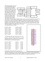
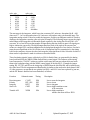
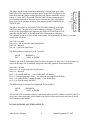
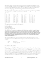
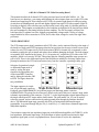
ARC-48: 8-Channel CCD Video Processing Board
This manual describes the 8-channel CCD video processor board, model ARC-48 Rev. 1A. The
board serves two functions - processing and digitizing the video outputs from one to eight CCD video
channels and supplying DC bias voltages to the CCD(s). It contains eight identical video processing
circuits that can simultaneously process and digitize signals from eight CCD video outputs. Eight 18bit analog-to-digital (A/D) converters are provided on the board, along with a 16-bit data pathway to
the backplane. Their outputs are multiplexed on the backplane on dedicated A/D data pins from which
they are transmitted by the timing board to the host computer. The DC bias supply section of the
board provides 32 separate low noise, digitally programmable voltages with a variety of voltage
ranges suitable for direct connection to CCDs, and a video offset voltage for each of the eight video
processors.
VIDEO PROCESSING
The CCD output source signal, sometimes called CCD video, can be connected directly to the input of
the board to a single-ended FET input stage that also has provision for the user to install a source load
resistor for each CCD output circuit. These load resistors (R203 in channel #0) are mounted on fork
terminals to enable the user to install and replace them without damaging the board. The load resistors
are normally NOT installed at the factory. A 0.1 μf capacitor AC couples the CCD video to the FET
amplifier, which is a low noise 2N5564. This preamp plus the following amplifier stage operates at a
gain of x2.8. There is also differential input to the board that is suitable for receiving outputs from
preamps located near the CCD and some meters away from the controller, operating at unity gain.
Selection of operation in single
or differential input mode is
made by wiring the input
signals to the appropriate pins
on the input DB67 connector
and by setting the switches SW1
to SW8. The figure shows the
two possibilities.
The input connector is a triple
row, 62-pin DB male connector,
Positronic part #ODD62M400T0. We generally supply the matching female connector
#ODD62F21000. The pinout for the connector is shown at the end of this user’s manual, along with a
schematic representation of the connector. Vin_H:0-7, are the high impedance signal inputs that go to
the single ended input FET stages and the load resistors. The pins named Vin_L-# can be used as
reference grounds, and are connected to the analog ground plane through the switches described
above. The differential input stage, generally driven by a low impedance differential output
preamplifier, is accessed through the pins Vin_L-# and Vin_L+#, which form a balanced input to the
differential amplifier.
Two resistors connect the low impedance input pins to the differential amplifier, the THS4131, of the
low impedance, differential input stage. We found them to induce significant noise into the high
impedance signal path, so have not populated them. If users desire to use the low impedance,
ARC-48 User's Manual
1
Updated September 27, 2007
differential input stage they need
to install 0805 SMT resistors in
the locations R214 and R213
shown in the figure of the back
of the board. For balanced inputs
such as would be supplied by a
differential preamp located next
to the CCD these two resistors
should have equal values, and
the gain of the stage is just the
value of the feedback resistor
divided by this input resistor.
The nominal values for R213
and R214 are 316 ohms, with the feedback resistors having a value of 630 ohms for a gain of x2. It is
also possible to connect unbalanced low impedance outputs to the differential input stage such as
might occur with simple source follower FET preamps. The low impedance negative side should be
grounded, and the resistor R213 on the positive side should be chosen so that the sum of the output
impedance preamp and the resistor R213 is about the same as the other resistor R214. This way the
differential amplifier will remain balanced. The various
video input pinouts are as follows:
Vin_H0 = pin 43
Vin_L-0 = pin 1
Vin_H1 = pin 44
Vin_L-1 = pin 2
Vin_H2 = pin 45
Vin_L-2 = pin 3
Vin_H3 = pin 46
Vin_L-3 = pin 4
Vin_H4 = pin 59
Vin_L-4 = pin 39
Vin_H5 = pin 60
Vin_L-5 = pin 40
Vin_H6 = pin 61
Vin_L-6 = pin 41
Vin_H7 = pin 62
Vin_L-7 = pin 42
The differential input stage, generally driven by a low
impedance differential output preamplifier, is accessed
through the pins Vin_L-# and Vin_L+#, which form a
balanced input to the differential amplifier.
Vin_L+0 = pin 22
Vin_L-0 = pin 1
Vin_L+1 = pin 23
Vin_L-1 = pin 2
Vin_L+2 = pin 24
Vin_L-2 = pin 3
Vin_L+3 = pin 25
Vin_L-3 = pin 4
Vin_L+4
Vin_L-4
Vin_L+5
Vin_L-5
Vin_L+6
Vin_L-6
Vin_L+7
Vin_L-7
pin 17
pin 39
pin 18
pin 40
pin 19
pin 41
pin 20
pin 42
This amplifier following the FET input stage has a
differential output that is connected to an analog switch that selects either inverted or non-inverted
output for accomplishing the correlated double sampling. The next stage is a programmable gain stage
that has fifteen gain selections that are software selectable according to the table below.
ARC-48 User's Manual
2
Updated September 27, 2007
code gain
0
5.625
1
5.250
2
4.875
3
4.500
4
4.125
5
3.750
6
3.375
7
3.000
code gain
8
2.625
9
2.250
10
1.875
11
1.500
12
1.125
13
0.750
14
0.375
15
forbidden
The next stage is the integrator, which has a time constant of 0.5 microsec, determined by R = 499
ohms and C = 1 nf. An integration time of 0.5 microsec will produce unity gain from this stage. The
integration analog switch is closed to enable the integrator, and the reset integrator switch is closed to
discharge the integration capacitor after each pixel is sampled. The following stages convert the single
ended output of the integrator to differential signals required by the Analog Devices AD7641 A/D
converter. It is a fast 18-bit part that samples its input during the time before its start A/D signal goes
high to initiate the conversion. The digital output data from each of the eight A/D converters are
written to a single FIFO, and then transmitted to the backplane through one of two latches. One latch
maps the most significant of the 18 A/D bits to the 16 backplane lines for transmission by the timing
board to the computer, whereas the other latch maps the least significant 16 bits. Selection of which of
these modes is operational is made in software as described below.
These fast timing signals, known collectively as SS# for Switch State, are generated by the timing
board, and latched by the WRSS (WRite Switch State) control signal. The software on the timing
board executes the “CLOCK” routine to read the switch state bits from waveform tables and write
them to the backplane along with the WRSS control signal. If the bits SS:15-12 match the jumper
setting JP9, JP7, JP5 and JP3 on the rising edge of WRSS then the bits SS6-SS0 will be latched onto
the video board. The bit assignment and functionality is similar to that used on the dual channel ARC45 video processor, except that the two polarity bits POL+ and POL- have been replaced by just one,
and the DC Restore function has been eliminated, as follows:
Function
Schematic name
Timing
Reset integrator
Polarity
Integrate
Start A/D
C_RST
INV_SIG
INTG
CNST
SS0
SS3
SS4
SS5
Transfer A/D
XFER
SS6
ARC-48 User's Manual
Description
Low to reset the integrator
Low to invert
Low to integrate
Low to high transition to start
A/D conversion
Low to high transition to
transfer data from A/Ds to FIFO
3
Updated September 27, 2007
The jumper header for the switch state addressing is located in the upper right
hand corner of the board next to the large surface mount PAL. The figure to the
right shows what the jumper headers look like, with jumpers installed to select a
logical “1” in the SS:15-12 bit field. The DAC and A/D select jumper headers
are also shown and will be discussed below. Generally the video board address
is set to zero in the software provided, so no jumpers should be installed in the
SWITCH field.
The gain is determined by the signals GAIN:3-0 routed identically to all eight
video processors. The gain value is set in software by writing a 25-bit serial
word over the synchronous serial interface pins TIM-A-SCK and TIM-A-STD,
generally with the XMIT_A_WORD in the ARC-22 timing board firmware.
The command is sent to all video boards in the system. The argument for the XMIT_A_WORD
command is as follows:
bits 23-20 = not used
bits 19-16 = %D, to select the video gain function
bits 15-4 = not used
bits 3-0 = gain code listed above
The DSP software to set the gain at x4.5 would be:
MOVE
JSR
#$0D0003,A
<XMIT_A_WORD
Similarly, the mode for transmitting either the lowest or highest 16- bits of the A/D 18 bit output is
done with the same sort of command, along with some other options to be discussed below:
bits 23-20 = not used
bits 19-16 = $C, to select the video board options
bits 15-4 = not used
bit 0 = 1 for WARP mode on; = 0 for WARP mode off (default)
bit 1 = 1 for least significant 16 bits; = 0 to select the most significant (default)
bit 2 = 1 to enable the DAC outputs (default); = 0 to disable them
bit 3 = 1 to clear the image data FIFO
The DSP software to select the least significant 16 bits would be:
MOVE
JSR
#$0C0002,A
<XMIT_A_WORD
All three bits #2-0 are written to latches on the board whenever the $C address is selected. If bit #3 is
set to a one a short reset pulse will be issued to the FIFOs on the board, and the three bits #2-0 will
also be written to the latches.
DC BIAS SUPPLIES AND VIDEO OFFSETS
ARC-48 User's Manual
4
Updated September 27, 2007
The DC bias voltages and video offsets are all generated by a single 40-channel digital-to-analog
converter (DAC), the Analog Devices part AD5379. It is programmed over the same synchronous
serial interface described above that sets the video gain. There are four DC bias supplies and one
video offset voltage supply allocated for driving each of the 8 channels of the CCD.
The table of available voltages follows, where names are assigned to suggest how a typical CCD is
operated. The Vrsv is named for “reserved” and is available for
general use.
Vod0 = pin 52
Vod1 = pin 32
Vod2 = pin 11
Vod3 = pin 53
Vod4 = pin 33
Vod5 = pin 12
Vod6 = pin 54
Vod7 = pin 34
Vrd0 pin 25
Vrd1 = pin 13
Vrd2 = pin 35
Vrd3 = pin 14
Vrd4 = pin 56
Vrd5 = pin 36
Vrd6 = pin 15
Vrd7 = pin 57
Vog0 = pin 29
Vog1 = pin 8
Vog2 = pin 50
Vog3 = pin 30
Vog4 = pin 9
Vog5 = pin 51
Vog6 = pin 31
Vog7 = pin 10
Vrsv0 = pin 5
Vrsv1 = pin 47
Vrsv2 = pin 27
Vrsv3 = pin 6
Vrsv4 = pin 48
Vrsv5 = pin 28
Vrsv6 = pin 7
Vrsv7 = pin 49
The approximate voltage range for each category is:
Vod = 0 to 30 volts
Vrd = 0 to 20 volts
Vog = Vrsv = -9 to +9 volts
The AD5379 DAC is a relatively complex part with 14-bit voltage resolution. It contains internal
registers that program the voltage as well as a gain and offset for each channel. Rather than fully
explain how the programming is done the user is referred to the part’s data sheet and the waveforms
file supplied with the board. The board address is encoded in each word written to the DAC in bits
D23-20, which must match the jumpers placed in the “DAC A/D” area described above, with a
jumper installed signifying a “1”.
The output of the DAC can be turned on and off in software. This is done on power-up in the
“timCCDmisc.asm” routine. Bit 2 of the board options word does this selection, so the command
would be:
MOVE
JSR
#$0C0004,A
<XMIT_A_WORD
; To turn on
IMAGE DATA TRANSFER
The four jumpers marked "DAC A/D" set the address that the board will respond to when writing to
the DC bias DAC or reading image data. These must be set to different values for each video board in
a system so each board can be uniquely addressed, whereas the “SWITCH” jumpers are usually set to
the same value for all video boards in the system so they all operate with the same timing. There are
two modes for transferring image data from the A/Ds to the image data FIFO. In the “eight-channelsall-at-once” mode (TIM_V_AUX1 = 0) all eight A/D values on each board are transferred in turn to
the image data FIFO on the rising edge of XFER. They will be transmitted over the backplane
ARC-48 User's Manual
5
Updated September 27, 2007
whenever the bits TIM-ADAD:6-3 match the jumpers "DAC A/D" on each video board starting with
A/D#0 and ending with A/D#7, ignoring the bits TIM-A-ADAD:2-0. In the 'one A/D at a time mode'
(TIM_V_AUX1 = 1) the addresses TIM_ADAD:2-0 select which of the eight A/Ds on the board gets
its data written to the FIFO, after which it is written directly to the backplane and transmitted to the
host computer. The default software supplied with the system has the “one-at-a-time” mode selected.
The image data FIFO can be cleared by setting bit 3 of the board options word:
MOVE
JSR
#$0C0008,A
<XMIT_A_WORD
; Clear image data FIFO
The AD converter has a special mode called WARP that allows it to run at a higher speed than the
normal mode, but with a restriction on the length of time allowed between conversions. To enable this
mode the WARP bit in the board options word is set:
MOVE
JSR
#$0C0001,A
<XMIT_A_WORD
; enable WARP mode
Note that all four options bits are written whenever the “C” address is selected, so care must be taken
when changing one mode not to change the other ones inadvertently.
ARC-48 User's Manual
6
Updated September 27, 2007