1
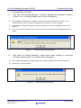
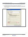
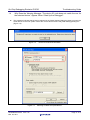
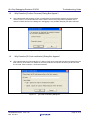
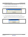
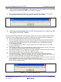
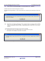
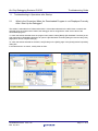
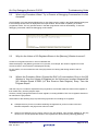
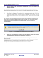
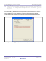
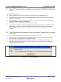
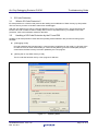
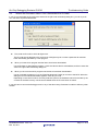
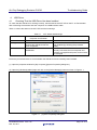
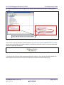
Application Notes
On-Chip Debugging Emulator E1/E20
Troubleshooting Guide (for the RX600 Series)
R20AN0045EJ0102
Rev.1.02
Mar. 29, 2011
Outline
This document gives examples of problems that may arise while using the E1 or E20 on-chip debugging
emulator in combination with RX600-series MCUs and remedies for these problems.
Some error messages vary with the version of the debugger. All examples given in this document use
E1/E20 Emulator Software V.1.01 Release 00.
R20AN0045EJ0102 Rev.1.02
Mar. 29, 2011
Page 1 of 21
On-Chip Debugging Emulator E1/E20
Troubleshooting Guide
Contents
1.
1.1
Troubleshooting on Startup ......................................................................................................................................................3
Why Does the Warning Message “Toolchain ‘Renesas RX Standard Toolchain’, version ‘x.xx.x’ is missing” Appear after
I Load a Workspace? ...............................................................................................................................................................3
1.2
Why Does the Warning Message “Target device driver missing, or connection cancelled” Appear When I Try to
1.3
Why is the [Emulator Serial No.] Section of the [Initial Settings] Dialog Box Blank?................................................................4
1.4
Why Does the Warning Message “The device ID code does not match the one for the selected device.” Appear When
1.5
Why Does the [Confirm Firmware] Dialog Box Appear? ..........................................................................................................6
1.6
Why Does the [ID Code verification] Dialog Box Appear? .......................................................................................................6
Start Up the Debugger? ...........................................................................................................................................................3
I Start Up the Debugger? .........................................................................................................................................................5
1.7
Why Does the Message “Includes invalid value or symbol:” Appear When I Enter an ID Code in the [ID Code verification]
Dialog Box? ..............................................................................................................................................................................7
1.8
Why Does the Message “Unable to connect to the emulator ()” Appear?................................................................................7
1.9
Why Does the Warning Message “Cannot detect the user system. Please check the connection between the emulator
and the user system.” Appear? ................................................................................................................................................8
1.10 Why Does the Warning Message “Power on the user system and press OK.” Appear? .........................................................8
1.11 Why Does the Warning Message “A timeout error. The command is not executable because the signal on the RESET pin
is active.” Appear?....................................................................................................................................................................9
1.12 Why Does the Warning Message “A JTAG communication error. Please retry with reducing the JTAG clock.” Appear?.......9
1.13 Why Does the Warning Message “A communication error.” Appear?....................................................................................10
1.14 Why Does the Warning Message “The emulator failed to connect with the MCU. There is a possibility that pin states or
operating mode of the MCU is not correct.” Appear?.............................................................................................................10
2.
Troubleshooting in Operations after Startup ..........................................................................................................................11
2.1
What is the Procedure When the Downloaded Program is not Displayed Correctly After I Start Up the Debugger? ............11
2.2
What is the Procedure When I Try to Execute a Debugging Command but It is Not Accepted? ...........................................12
2.3
Why Are the Values of I/O Registers Shown in the [Memory] Window Incorrect? .................................................................12
2.4
What is the Procedure When I Expand the RIIC (I C bus interface) Entry in the [IO] Window to View the Values of
2
2
Registers but the Values are Incorrect because the [IO] Window Reads ICDRR (I C Bus Receive Data Register)
Every Time the Program Stops? ............................................................................................................................................12
2.5
Why Do Values in Data Flash Memory Change Every Time I View Them in the [Memory] Window? ...................................13
2.6
Why Does the Message “The setting of the peripheral module clock (PCLK) is outside the range. Please check the
setting of the input clock (EXTAL) and the system and the system clock control register (SCKCR).” Appear and
Programming Fail? .................................................................................................................................................................13
2.7
What is the Procedure When Rewriting the Flash Memory through the Program Succeeded with the Emulator
2.8
What is the Procedure When the Debugger Cannot Read the Latest Values from Location in the On-Chip Flash Memory
2.9
Why Don’t Values Change as Expected during Realtime RAM Monitoring by the E20? .......................................................15
but Failed with the Actual MCU? ............................................................................................................................................13
That Have been Altered by a User Program? ........................................................................................................................14
2.10 Why Does the Warning Message “Not enough memory” Appear When I Download a Program? .........................................15
3.
ID-Code Protection .................................................................................................................................................................16
3.1
What is ID-Code Protection? ..................................................................................................................................................16
3.2
Handling of ID-Code Protection by the E1 and E20 ...............................................................................................................16
3.3
What is the Procedure When I Don’t Remember the ID Code? .............................................................................................17
4.
USB Driver..............................................................................................................................................................................18
4.1
Checking That the USB Driver Has been Installed ................................................................................................................18
R20AN0045EJ0102 Rev.1.02
Mar. 29, 2011
Page 2 of 21
On-Chip Debugging Emulator E1/E20
1.
1.1
Troubleshooting Guide
Troubleshooting on Startup
Why Does the Warning Message “Toolchain ‘Renesas RX Standard Toolchain’,
version ‘x.xx.x’ is missing” Appear after I Load a Workspace?
z
This message indicates that a compatible compiler has not been installed or the version of the
compiler that was used to create the workspace is not present on the host computer.
z
Newly install a compatible compiler or follow the instructions to select a compatible version of the
compiler.
z
If you do not need to execute a build, you can ignore this message and start debugging with the E1
or E20.
Figure 1.1
1.2
Compiler Version Does Not Match
Why Does the Warning Message “Target device driver missing, or connection
cancelled” Appear When I Try to Start Up the Debugger?
z
This message appearing first indicates that the E1 and E20 software has not been installed yet.
z
Install the E1 and E20 software.
Figure 1.2
R20AN0045EJ0102 Rev.1.02
Mar. 29, 2011
Target Device Driver Missing
Page 3 of 21
On-Chip Debugging Emulator E1/E20
1.3
z
Troubleshooting Guide
Why is the [Emulator Serial No.] Section of the [Initial Settings] Dialog Box Blank?
This indicates that the host computer has not recognized the E1 or E20 emulator.
Check that the USB cable is correctly connected and, if you are using the E20, that the power switch
on the E20 is ON, and then click on the [Refresh] button. If a serial number is still not displayed, refer
to section 4, USB Driver.
Figure 1.3
R20AN0045EJ0102 Rev.1.02
Mar. 29, 2011
Emulator Serial Number Not Displayed
Page 4 of 21
On-Chip Debugging Emulator E1/E20
Troubleshooting Guide
1.4
Why Does the Warning Message “The device ID code does not match the one for
the selected device.” Appear When I Start Up the Debugger?
z
This message indicates that the device selected in the [Initial Settings] dialog box does not match the
actual device on the user system. Select the correct device name in the [Initial Settings] dialog box
(Figure 1.5).
Figure 1.4
Figure 1.5
R20AN0045EJ0102 Rev.1.02
Mar. 29, 2011
Device ID Code Does Not Match
Selecting an MCU Group and Device
Page 5 of 21
On-Chip Debugging Emulator E1/E20
1.5
z
Why Does the [Confirm Firmware] Dialog Box Appear?
This indicates that the firmware version corresponding to the emulator software and the firmware
version in the E1 or E20 emulator are not the same. Click on the [Yes] button regardless of the
version numbers shown in the dialog box. Debugging is not possible after [No] has been selected.
Figure 1.6
1.6
z
Troubleshooting Guide
[Confirm Firmware] Dialog Box
Why Does the [ID Code verification] Dialog Box Appear?
This indicates that ID-code protection is in effect. Enter the ID code that has been programmed in the
flash memory of the MCU. For details on ID-code protection and what to do when you do not know
the ID code, refer to section 3, ID-Code Protection.
Figure 1.7
R20AN0045EJ0102 Rev.1.02
Mar. 29, 2011
[ID Code verification] Dialog Box
Page 6 of 21
On-Chip Debugging Emulator E1/E20
1.7
Troubleshooting Guide
Why Does the Message “Includes invalid value or symbol:” Appear When I Enter
an ID Code in the [ID Code verification] Dialog Box?
z
This message indicates that the entered ID code was incorrect.
z
Check the ID code again. The ID code must consist of 32 bits, including the control code.
Figure 1.8
1.8
z
Includes Invalid Value or Symbol
Why Does the Message “Unable to connect to the emulator ()” Appear?
This message indicates that the E1 or E20 emulator is not correctly connected to the host computer.
Refer to section 1.3, Why is the [Emulator Serial No.] Section of the [Initial Settings] Dialog Box
Blank?.
Figure 1.9
R20AN0045EJ0102 Rev.1.02
Mar. 29, 2011
Unable to Connect to the Emulator
Page 7 of 21
On-Chip Debugging Emulator E1/E20
1.9
z
z
z
Why Does the Warning Message “Cannot detect the user system. Please check
the connection between the emulator and the user system.” Appear?
Check that the E1 or E20 connector is firmly connected to the user system.
If you are using the E1, check that pin 14 of the emulator connector is connected to GND. The E1
recognizes the connection of the user system when it detects that this pin is at the low level.
If you are using the E20, check that pin 5 of the emulator connector is connected to GND. The E20
recognizes the connection of the user system when it detects that this pin is at the low level.
Figure 1.10
1.10
z
z
Troubleshooting Guide
Cannot Detect the User System
Why Does the Warning Message “Power on the user system and press OK.”
Appear?
Check that the user system is supplied with power.
Check that the VCC pin of the emulator connector is connected to VCC on the user system.
Figure 1.11
R20AN0045EJ0102 Rev.1.02
Mar. 29, 2011
Turn the Power on
Page 8 of 21
On-Chip Debugging Emulator E1/E20
1.11
z
Troubleshooting Guide
Why Does the Warning Message “A timeout error. The command is not executable
because the signal on the RESET pin is active.” Appear?
This message indicates that the MCU cannot be reset. Ensure that the RES# pin of the emulator
connector and the reset circuit on the user system are not fixed to the low level.
Figure 1.12
1.12
Timeout Error
Why Does the Warning Message “A JTAG communication error. Please retry with
reducing the JTAG clock.” Appear?
This message indicates that the MCU cannot operate normally or the connection between the MCU and the
emulator is incorrect. Although there are a number of possible causes, typical examples are listed below.
z
z
z
z
z
z
z
z
Check the connection between the MCU and the emulator connector.
When an RX610-group MCU is in use, the connection pattern between the MCU and the emulator
connector depends on whether the emulator is being used as an on-chip debugging emulator or in
the boot mode. Check that the emulator connector (attached to the E1 or E20) is the one for an
on-chip debugging emulator.
If you are using an extension cable to connect the MCU and the emulator connector, try using a
standard cable instead.
Check whether a filtering circuit is placed between the MCU and the emulator connector. If this is the
case, temporarily remove the filtering circuit and check the operation.
Check that the handling of pins necessary for the correct operation of the MCU (pins associated with
power supply and reset, e.g. VCC, GND, VCL, RESET) is correct.
Check that the oscillator circuit connected to the MCU is operating correctly.
Check that the EMLE pin is pulled-down (this pin must not be directly connected to GND) and
connected to the emulator connector. If the EMLE pin is not connected to the emulator connector, the
pin must be manually switched to the high level before debugging proceeds.
If you are using the E20, check that the GND bus lead of the Mictor connector is correctly connected
to GND (“GND bus lead” refers to the pin at the center of the connector).
Pin 5 of the Mictor connector is not GND. Failure to correctly connect the bus lead to GND will lead to
this error and to unstable operation.
Figure 1.13
R20AN0045EJ0102 Rev.1.02
Mar. 29, 2011
JTAG Communication Error
Page 9 of 21
On-Chip Debugging Emulator E1/E20
1.13
Troubleshooting Guide
Why Does the Warning Message “A communication error.” Appear?
Possible causes are the same as those given in section 0,
Why Does the Warning Message “A JTAG communication error. Please retry with reducing the JTAG clock.”
Appear?.
Figure 1.14
1.14
Communication Error
Why Does the Warning Message “The emulator failed to connect with the MCU.
There is a possibility that pin states or operating mode of the MCU is not correct.”
Appear?
This message indicates that the emulator cannot connect to the MCU.
z
Ensure that the levels on pins MD0 and MD1 are not those for the boot mode.
The emulator cannot establish a connection in boot mode.
Figure 1.15
R20AN0045EJ0102 Rev.1.02
Mar. 29, 2011
Emulator Failed to Connect with the MCU
Page 10 of 21
On-Chip Debugging Emulator E1/E20
2.
2.1
Troubleshooting Guide
Troubleshooting in Operations after Startup
What is the Procedure When the Downloaded Program is not Displayed Correctly
After I Start Up the Debugger?
The endian is selectable for a RX600-series MCU. If the endian selected for the MCU does not match that
selected when the program was created, the debugger cannot recognize the reset vector value of the
downloaded program.
To check the endian selected when the program was created, select [Build]->[RX Standard Toolchain] in the
High-performance Embedded Workshop to open the [RX Standard Toolchain] dialog box and see the [CPU]
page (which shows compiler settings).
To check the endian selected for the MCU, see [Endian] on the [MCU] page of the [Configuration Properties]
dialog box.
If the selections do not match, modify either of them.
The two must
match.
Compiler settings
R20AN0045EJ0102 Rev.1.02
Mar. 29, 2011
MCU settings
Page 11 of 21
On-Chip Debugging Emulator E1/E20
2.2
Troubleshooting Guide
What is the Procedure When I Try to Execute a Debugging Command but It is Not
Accepted?
Check whether you have selected [Writing the on-chip flash memory mode] in the [Initial Settings] dialog box.
If the message shown below is displayed in the output window, the emulator is operating in the flash
programmer mode. The only possible action in the flash programmer mode is downloading. To execute
debugging commands, select the debugging mode instead.
Figure 2.1
2.3
Display in the Output Window
Why Are the Values of I/O Registers Shown in the [Memory] Window Incorrect?
Access to I/O registers must be in units of a defined size.
When the display in the [Memory] window is in byte units, for example, the values of registers for which
access must be in word units are not displayed correctly.
For this reason, we recommend the use of the [IO] window for viewing and setting values of the I/O
registers.
2.4
What is the Procedure When I Expand the RIIC (I2C bus interface) Entry in the [IO]
Window to View the Values of Registers but the Values are Incorrect because the
[IO] Window Reads ICDRR (I2C Bus Receive Data Register) Every Time the
Program Stops?
After the entry for a module is expanded in the [IO] window, the window reads the values of the registers of
that module every time the program stops.
However, reading changes the states of some registers, including ICDRR in RIIC. Such registers should not
be read from the [IO] window.
Select either of the following ways to prevent the [IO] window from reading such registers.
z
Collapse the entry for the IO module containing the register that you do not want to be read.
Modules collapsed in the [IO] window will not be read.
z
Select [Lock Refresh] from the popup menu of the [IO] window. This prevents reading for the [IO]
window. You can still update the values of I/O registers at a desired time by selecting [Refresh].
R20AN0045EJ0102 Rev.1.02
Mar. 29, 2011
Page 12 of 21
On-Chip Debugging Emulator E1/E20
2.5
Troubleshooting Guide
Why Do Values in Data Flash Memory Change Every Time I View Them in the
[Memory] Window?
The default state (immediately after erasure) of the Data Flash in RX600-series MCUs is undefined so
different values are read out every time. This is simply one of the MCU’s specifications and is not a defect.
2.6
Why Does the Message “The setting of the peripheral module clock (PCLK) is
outside the range. Please check the setting of the input clock (EXTAL) and the
system and the system clock control register (SCKCR).” Appear and Programming
Fail?
The combination of the value specified for [Input clock (EXTAL)] in the [Configuration Properties] dialog box
and the setting of the peripheral module clock selection bits in the system clock control register (SCKCR)
produces a frequency beyond the allowed range of peripheral-module clock (PCLK) frequencies.
Check both settings.
Figure 2.2
2.7
Peripheral-Module Clock (PCLK) Designation is out of Bounds
What is the Procedure When Rewriting the Flash Memory through the Program
Succeeded with the Emulator but Failed with the Actual MCU?
The data in the FCU ROM must be transferred to the FCU RAM before rewriting the flash memory in an
RX600-series MCU.
When the emulator is in use, the emulator program transfers data from the FCU ROM to the FCU RAM, so
rewriting the flash memory is possible even if the user program does not handle the transfer.
For usage of the FCU ROM and FCU RAM, refer to the user’s manual for the MCU.
R20AN0045EJ0102 Rev.1.02
Mar. 29, 2011
Page 13 of 21
On-Chip Debugging Emulator E1/E20
2.8
Troubleshooting Guide
What is the Procedure When the Debugger Cannot Read the Latest Values from
Location in the On-Chip Flash Memory That Have been Altered by a User
Program?
Since caching of the on-chip flash memory on the host computer is enabled by default, it is not possible to
read the most recently updated values from the on-chip flash memory.
If the on-chip flash memory is to be updated by a user program, select the [Debugging the program
re-writing the internal flash.] checkbox on the [System] page of the [Configuration Properties] dialog box.
Figure 2.3
Debugging of Programs That Involve Rewriting of the On-Chip Flash Memory
R20AN0045EJ0102 Rev.1.02
Mar. 29, 2011
Page 14 of 21
On-Chip Debugging Emulator E1/E20
2.9
Troubleshooting Guide
Why Don’t Values Change as Expected during Realtime RAM Monitoring by the
E20?
Check the following points.
z
[Realtime RAM monitor] must be selected in the [Configuration Properties] dialog box.
z
Automatic variables cannot be monitored by realtime RAM monitoring because values are stored in
registers or on the stack.
z
If optimization by the compiler eliminates a variable to be monitored or its assignment, declare the
variable as volatile to prevent this optimization.
z
DMA access cannot be monitored by realtime RAM monitoring.
z
Monitoring of I/O registers for which the values are constantly being updated is not possible because
realtime RAM monitoring is actually realized by monitoring reading and writing of memory by the
MCU. Detecting changes of values in areas that are not read or written by programs is thus not
possible.
2.10
Why Does the Warning Message “Not enough memory” Appear When I Download
a Program?
z
This message indicates that the destination is an access-prohibited area.
z
See the memory map in the hardware manual for the MCU and check that the download module
does not include a reserved area (access-prohibited area).
z
If the download module includes external address space, check that [Single-chip mode] is not
selected in the [Operating mode] section of the [Configuration Properties] dialog box that appears
when the emulator is booted up.
Figure 2.4
R20AN0045EJ0102 Rev.1.02
Mar. 29, 2011
Not Enough Memory
Page 15 of 21
On-Chip Debugging Emulator E1/E20
3.
3.1
Troubleshooting Guide
ID-Code Protection
What is ID-Code Protection?
ID-code protection is a function that prevents the reading and modification of flash memory by third parties.
This is a security function of the MCU rather than the debugger.
After the user writes an ID code to a specific address in the on-chip flash memory, anyone who does not
know the ID code is unable to read or modify data in the on-chip flash memory. For details on ID-code
protection, refer to the hardware manual for the MCU.
3.2
Handling of ID-Code Protection by the E1 and E20
Handling of ID-code protection varies with the operating mode selected in the process of booting up the
emulator.
z
[Debugging mode]
ID-code protection that has been set by a user program is ineffective in this mode (i.e. all bytes of the
ID code are FF even when downloading or control via the [Memory] window is attempted) except in
cases where the flash memory has been updated by the user program.
z
[Writing the on-chip flash memory mode]
The ID code that has been set by a user program is effective.
Figure 3.1
R20AN0045EJ0102 Rev.1.02
Mar. 29, 2011
Operating Mode
Page 16 of 21
On-Chip Debugging Emulator E1/E20
3.3
Troubleshooting Guide
What is the Procedure When I Don’t Remember the ID Code?
If you do not remember the ID code to be entered in the [ID Code verification] dialog box, you can try to do
so in the three ways described below.
Figure 3.2
z
[ID Code verification] Dialog Box
First, enter an ID code in which all digits are 0.
The ID code area is adjacent to the vector area. All digits may be 0 unless a particular ID code has
been intentionally specified by a user program.
z
When you know which program was the last to have been downloaded
Use a simulator to download the program, check the value at the ID-code address, and then enter that
value in the [ID Code verification] dialog box.
z
When you do not know which program was the last to have been downloaded
Use an on-board programmer (e.g. the Flash Development Toolkit) to connect to the MCU. When the
dialog box for ID-code authentication appears, enter any ID code.
Depending on the control code for ID-code protection (refer to the hardware manual for the MCU), the
contents of the flash memory can become erasable when the ID code does not match.
If you still cannot connect the debugger even in any of the above ways, Renesas is unable to offer any other
solution.
R20AN0045EJ0102 Rev.1.02
Mar. 29, 2011
Page 17 of 21
On-Chip Debugging Emulator E1/E20
4.
4.1
Troubleshooting Guide
USB Driver
Checking That the USB Driver Has been Installed
To check that the USB driver is working correctly, see the state of the ACT LED on the E1 or E20 emulator
after connecting the emulator and host computer via a USB interface cable.
Table 4.1 shows the states of the ACT LED and their meanings.
Table 4.1
ACT LED
Illuminated
Blinking
Not illuminated
ACT States and Meanings
Communication between the Host
Computer and Emulator
The emulator is usable.
The emulator is not usable yet
because the USB driver has not
been recognized.
Communication has not been
established.
Checkpoint
The USB driver has correctly been installed.
Check whether the USB driver has correctly
been installed (by following the procedure
below).
Check whether the USB interface cable is
correctly connected, the host computer and
emulator are supplied with power, and no items
are damaged.
Follow the procedures below to check whether the USB driver has successfully been installed.
(1) Open the properties window for [My Computer] ([System Properties] dialog box).
(2) Open the [Hardware] tabbed page and click on the [Device Manager] button as shown in Figure 4.1.
Figure 4.1
R20AN0045EJ0102 Rev.1.02
Mar. 29, 2011
[System Properties] Dialog Box
Page 18 of 21
On-Chip Debugging Emulator E1/E20
Troubleshooting Guide
(3) Check that [Renesas E-Series USB Driver] is shown under the [Renesas Emulator] category (Figure
4.2).
Check that the USB driver has been installed.
Figure 4.2
Device Manager
Some drivers under the [Renesas Emulator] category may have a [!] or [?] mark attached to the icon. These
drivers may not have been successfully installed, so delete them, disconnect and re-connect the USB cable,
and then re-install the USB drivers.
Figure 4.3
Display Indicating Failed Installation of a USB Driver
If you cannot find any driver under the [Renesas Emulator] category, check that the emulator software has
been installed, disconnect and re-connect the USB cable, and then re-install the USB drivers.
R20AN0045EJ0102 Rev.1.02
Mar. 29, 2011
Page 19 of 21
On-Chip Debugging Emulator E1/E20
Troubleshooting Guide
Website and Support
Renesas Electronics Tools Website
http://www.renesas.com/tools
Inquiries
http://www.renesas.com/inquiry
Revision History
Rev.
1.01
1.02
Date
Jan. 16, 2011
Mar. 29, 2011
Page
—
—
Description
Summary
Newly created
The reference origin of "3.ID-Code Protection" is changed.
All trademarks and registered trademarks belong to their respective owners.
R20AN0045EJ0102 Rev.1.02
Mar. 29, 2011
Page 20 of 21
On-Chip Debugging Emulator E1/E20
Troubleshooting Guide
Notice
1.
All information included in this document is current as of the date this document is issued. Such information, however, is subject to change without any prior notice. Before purchasing or using any Renesas
Electronics products listed herein, please confirm the latest product information with a Renesas Electronics sales office. Also, please pay regular and careful attention to additional and different information to
be disclosed by Renesas Electronics such as that disclosed through our website.
2.
Renesas Electronics does not assume any liability for infringement of patents, copyrights, or other intellectual property rights of third parties by or arising from the use of Renesas Electronics products or
technical information described in this document. No license, express, implied or otherwise, is granted hereby under any patents, copyrights or other intellectual property rights of Renesas Electronics or
others.
3.
You should not alter, modify, copy, or otherwise misappropriate any Renesas Electronics product, whether in whole or in part.
4.
Descriptions of circuits, software and other related information in this document are provided only to illustrate the operation of semiconductor products and application examples. You are fully responsible for
the incorporation of these circuits, software, and information in the design of your equipment. Renesas Electronics assumes no responsibility for any losses incurred by you or third parties arising from the
use of these circuits, software, or information.
5.
When exporting the products or technology described in this document, you should comply with the applicable export control laws and regulations and follow the procedures required by such laws and
regulations. You should not use Renesas Electronics products or the technology described in this document for any purpose relating to military applications or use by the military, including but not limited to
the development of weapons of mass destruction. Renesas Electronics products and technology may not be used for or incorporated into any products or systems whose manufacture, use, or sale is
prohibited under any applicable domestic or foreign laws or regulations.
6.
Renesas Electronics has used reasonable care in preparing the information included in this document, but Renesas Electronics does not warrant that such information is error free. Renesas Electronics
7.
Renesas Electronics products are classified according to the following three quality grades: "Standard", "High Quality", and "Specific". The recommended applications for each Renesas Electronics product
assumes no liability whatsoever for any damages incurred by you resulting from errors in or omissions from the information included herein.
depends on the product's quality grade, as indicated below. You must check the quality grade of each Renesas Electronics product before using it in a particular application. You may not use any Renesas
Electronics product for any application categorized as "Specific" without the prior written consent of Renesas Electronics. Further, you may not use any Renesas Electronics product for any application for
which it is not intended without the prior written consent of Renesas Electronics. Renesas Electronics shall not be in any way liable for any damages or losses incurred by you or third parties arising from the
use of any Renesas Electronics product for an application categorized as "Specific" or for which the product is not intended where you have failed to obtain the prior written consent of Renesas Electronics.
The quality grade of each Renesas Electronics product is "Standard" unless otherwise expressly specified in a Renesas Electronics data sheets or data books, etc.
"Standard":
Computers; office equipment; communications equipment; test and measurement equipment; audio and visual equipment; home electronic appliances; machine tools;
personal electronic equipment; and industrial robots.
"High Quality": Transportation equipment (automobiles, trains, ships, etc.); traffic control systems; anti-disaster systems; anti-crime systems; safety equipment; and medical equipment not specifically
designed for life support.
"Specific":
Aircraft; aerospace equipment; submersible repeaters; nuclear reactor control systems; medical equipment or systems for life support (e.g. artificial life support devices or systems), surgical
implantations, or healthcare intervention (e.g. excision, etc.), and any other applications or purposes that pose a direct threat to human life.
8.
You should use the Renesas Electronics products described in this document within the range specified by Renesas Electronics, especially with respect to the maximum rating, operating supply voltage
range, movement power voltage range, heat radiation characteristics, installation and other product characteristics. Renesas Electronics shall have no liability for malfunctions or damages arising out of the
use of Renesas Electronics products beyond such specified ranges.
9.
Although Renesas Electronics endeavors to improve the quality and reliability of its products, semiconductor products have specific characteristics such as the occurrence of failure at a certain rate and
malfunctions under certain use conditions. Further, Renesas Electronics products are not subject to radiation resistance design. Please be sure to implement safety measures to guard them against the
possibility of physical injury, and injury or damage caused by fire in the event of the failure of a Renesas Electronics product, such as safety design for hardware and software including but not limited to
redundancy, fire control and malfunction prevention, appropriate treatment for aging degradation or any other appropriate measures. Because the evaluation of microcomputer software alone is very difficult,
please evaluate the safety of the final products or system manufactured by you.
10. Please contact a Renesas Electronics sales office for details as to environmental matters such as the environmental compatibility of each Renesas Electronics product. Please use Renesas Electronics
products in compliance with all applicable laws and regulations that regulate the inclusion or use of controlled substances, including without limitation, the EU RoHS Directive. Renesas Electronics assumes
no liability for damages or losses occurring as a result of your noncompliance with applicable laws and regulations.
11. This document may not be reproduced or duplicated, in any form, in whole or in part, without prior written consent of Renesas Electronics.
12. Please contact a Renesas Electronics sales office if you have any questions regarding the information contained in this document or Renesas Electronics products, or if you have any other inquiries.
(Note 1)
(Note 2)
"Renesas Electronics" as used in this document means Renesas Electronics Corporation and also includes its majority-owned subsidiaries.
"Renesas Electronics product(s)" means any product developed or manufactured by or for Renesas Electronics.
SALES OFFICES
http://www.renesas.com
Refer to "http://www.renesas.com/" for the latest and detailed information.
Renesas Electronics America Inc.
2880 Scott Boulevard Santa Clara, CA 95050-2554, U.S.A.
Tel: +1-408-588-6000, Fax: +1-408-588-6130
Renesas Electronics Canada Limited
1101 Nicholson Road, Newmarket, Ontario L3Y 9C3, Canada
Tel: +1-905-898-5441, Fax: +1-905-898-3220
Renesas Electronics Europe Limited
Dukes Meadow, Millboard Road, Bourne End, Buckinghamshire, SL8 5FH, U.K
Tel: +44-1628-585-100, Fax: +44-1628-585-900
Renesas Electronics Europe GmbH
Arcadiastrasse 10, 40472 Düsseldorf, Germany
Tel: +49-211-6503-0, Fax: +49-211-6503-1327
Renesas Electronics (China) Co., Ltd.
7th Floor, Quantum Plaza, No.27 ZhiChunLu Haidian District, Beijing 100083, P.R.China
Tel: +86-10-8235-1155, Fax: +86-10-8235-7679
Renesas Electronics (Shanghai) Co., Ltd.
Unit 204, 205, AZIA Center, No.1233 Lujiazui Ring Rd., Pudong District, Shanghai 200120, China
Tel: +86-21-5877-1818, Fax: +86-21-6887-7858 / -7898
Renesas Electronics Hong Kong Limited
Unit 1601-1613, 16/F., Tower 2, Grand Century Place, 193 Prince Edward Road West, Mongkok, Kowloon, Hong Kong
Tel: +852-2886-9318, Fax: +852 2886-9022/9044
Renesas Electronics Taiwan Co., Ltd.
7F, No. 363 Fu Shing North Road Taipei, Taiwan, R.O.C.
Tel: +886-2-8175-9600, Fax: +886 2-8175-9670
Renesas Electronics Singapore Pte. Ltd.
1 harbourFront Avenue, #06-10, keppel Bay Tower, Singapore 098632
Tel: +65-6213-0200, Fax: +65-6278-8001
Renesas Electronics Malaysia Sdn.Bhd.
Unit 906, Block B, Menara Amcorp, Amcorp Trade Centre, No. 18, Jln Persiaran Barat, 46050 Petaling Jaya, Selangor Darul Ehsan, Malaysia
Tel: +60-3-7955-9390, Fax: +60-3-7955-9510
Renesas Electronics Korea Co., Ltd.
11F., Samik Lavied' or Bldg., 720-2 Yeoksam-Dong, Kangnam-Ku, Seoul 135-080, Korea
Tel: +82-2-558-3737, Fax: +82-2-558-5141
R20AN0045EJ0102 Rev.1.02
Mar. 29, 2011
Page 21 of 21