1
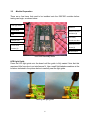
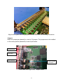
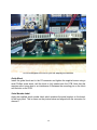
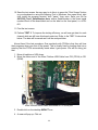
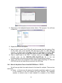
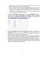
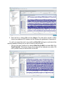
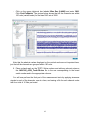
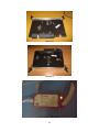
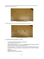
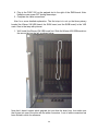
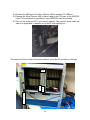
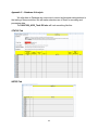
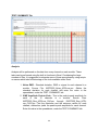
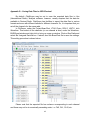
Assembly and Testing of the fADC250 Modules at UMass
F. Ahmed (UMass), F.J. Barbosa, H. Dong, E. Jastrjembski and J. Wilson (JLab)
24 June 2012
Index
1. Introduction
2. What is the fADC250?
3. Test Setup
3.0
Recording Information
3.1
Receiving & Visual Inspection
3.2
Module Preparation
3.3
Burn-in Test
3.4
Program and Test
3.4.1 Programming & Testing the fADC250 Board – Test 1
3.4.2 Noise & Amplitude Tests of the fADC250 Board – Test 2
4. Logging, Inspection & Shipping
5. Appendices
5.1
Appendix A - Test Equipment Setup
5.2
Appendix B – Software & Installation
5.3
Appendix C – Database & Analysis
5.4
Appendix D – Saving Data Files in ASCII Decimal
1
1
4
5
5
6
13
15
18
24
29
30
40
43
45
1. Introduction
This document will lead you through the entire test procedure for the fADC250. It
also assumes that you don't have much knowledge of electronics and how to test
electronics boards. A person with no skills in electronics can go through this test
procedure; this document is written so that the same person can read this document
and come out with the knowledge to perform this task.
2. What is the fADC250?
Before I get into describing the test procedure for the fADC250, let me briefly tell
you what the fADC250 is. In short, it is a circuit board that has been programmed (and
can be programmed at will) to use up to 16 ADCs (ADCs are explained in the next
paragraph) to capture small, high frequency electrical signals. One use, for instance, is
to record light signals detected in high energy physics experiments that involve
measuring light. Normally, the light is converted to photo-electrons and amplified by a
photomultiplier tube; the output pulses are sampled and recorded as data by the
fADC250.
1
An analog to digital converter, abbreviated as ADC, takes information from the
real world (whether it's music, pictures, text, etc) and saves it as a sequence of 0's and
1's, so you can save it to computer storage media like hard drives and memory cards.
For instance, when you take a picture with a digital camera that saves on a memory
stick as opposed to film, you can guarantee that an analog to digital converter does the
work of converting the picture into a sequence of 0's and 1's that eventually get written
to the memory stick. Now there are more steps between converting the real world
information to 0's and 1's, and actually writing the 0's and 1's to the memory stick. For
our fADC250, those steps are handled by the two FPGAs. In simple terms, one FPGA
processes the data and the other FPGA handles communications for data readout
through the backplane of the VXS crate.
An FPGA, field programmable gate array, is a chip that can be programmed to
execute any program you can think of, as long as it has enough logic circuits to execute
your program. Its flexibility makes it an incredibly attractive choice for designs, like this
one. You could, theoretically, use the same FPGA as the CPU of your computer, in a
calculator, in a graphics card, in a camera, in your microwave, and so on. In fact, you
can actually program a processor onto the chip, then write C/java/python etc code that
compiles and executes on that programmed processor. The main caveat to an FPGA is
that it will operate much more slowly (often more than ten times slower!) than a chip
custom designed to do the same task, and usually the FPGA is much less expensive
than a dedicated chip (ASIC). Prototypes and low volume products are typically done
with FPGAs, where as the final product that is mass produced has the dedicated chips
(ASICs).
The 250 in "fADC250" stands for 250MHz (Megahertz), the rate at which the
ADC samples analog data at its inputs. You can interpret "250 MHz" two ways and you
should pick both ways: every second, the ADC has done its task 250 million times.
Every 250 millionths of a second, the ADC has done its task. To keep going with the
picture analogy, consider a video camera. A video is just a sequence of pictures, and in
U.S. television, videos have 30 pictures or frames per second. The ADC inside the
video cameras used for television work operates at rates in the range of 100’s of MHz to
provide good resolution or fine detail (pixels) over the picture area of interest and each
picture frame is available at a rate of 30 Hz. Generally, the sampling rate should be
twice as fast as the bandwidth of interest, known as the Nyquist rate. Movies are shot at
a rate of 24 pictures per second, or 24 Hz. Now if you were going to use the ADC of the
fADC250 in the video camera, each second of film would have 250 million samples!
That’s a lot of information that needs to be processed, stored and transmitted. Picture
files can be very big (over 2 megabytes) and some filtering and compression may be
necessary.
Front panel view.
2
Rear view.
Perspective view.
Up close view of the front panel, focusing on the first six ADC channels.
B21595_21R is the serial number of this board.
The two FPGAs - you'll see them more in depth in the board assembly instructions.
3
The 16 ADCs. Note the symmetry in how they are designed.
3. Test Setup
A number of work benches should be prepared and reserved for testing the
fADC250 modules and depending on space availability and lab organization. The test
area must be prepared in a manner that minimizes the risk of electro-static discharges
by employing ESD mats. ESD mats have slightly resistive surfaces and are grounded
by means of supplied cables to an outlet ground, for example. There are bench and
floor ESD mats available and it is important to always keep all surfaces clean and free
from dust. This is especially important in dry environments. The test work flow is shown
below:
Module
Preparation
&
Burn-in
Program
&
Test
Receiving
&
Inspection
Logging,
Inspection
&
Shipping
Test Work Flow
Test Protocol
There are a number of steps to be performed and in the following order:
1. Receiving & Visual Inspection
2. Module Preparation
4
3. Burn-in Test
4. Program and Test
5. Logging, Inspection & Shipping
3.0
Recording Information
All the information obtained during testing will be recorded to build a history of
each fADC250 module. This information is very important and it will be very useful for
diagnosing systematic problems during the assembly process and for tracking long term
performance during the life cycle of the product.
For example, a module may not pass its tests because of a manufacturing error
during fabrication of the printed circuit board (PCB) or because of a component is
defective or out of tolerance or even because a component is not properly soldered.
There is also the possibility that a step during testing was not properly followed.
Our test database will be built based on a supplied and pre-configured Excel file.
The file name is fADC250_ACDI_TestLOG.xlsx. This file is pre-filled with sequentially
listed serial numbers and column headings such as Serial Number, Inspection Date,
Personnel, Notes, etc.
This file will be accessed often to enter the requested test observations and
should be available on a PC at all times during testing.
3.1
Receiving & Visual Inspection
Carefully inspect the boxes received from the manufacturer and its contents.
Record your observations, shipping information and date. Note the packaging
organization and materials as these will be used for shipping the tested modules to
JLab.
Each fADC250 module is wrapped in an ESD package and has a label with its
serial number. Observe the ESD precautions and carefully remove the board from its
ESD wrapping. Inspect the board visually to check for missing or incorrectly installed
components. Perform a second visual inspection under the microscope to check the
quality of solder joints at a few locations. Based on known good modules shown during
training, this step should take no longer than 5 minutes. Record the date and add any
relevant notes on the fADC250_ACDI_TestLOG.xlsx file in the row corresponding to
the board serial number and in the appropriate columns.
5
3.2
Module Preparation
There are a few items that need to be installed onto the fADC250 modules before
testing can begin, as shown below.
LED Light Guide
Heatsink
Front Panel
PCB
Heatsink Screws
and Nuts (4)
Jumper (16)
Thermally
Conductive Mat
Guide Block and
Screw (1)
Front Panel
Screws (2)
P0 Connector
fADC250 Assembly Items
LED Light Guide
Press the LED light guide onto the board until the guide is fully seated. Note that this
requires a little force due to an interference fit. Use a small flat-bladed screwdriver at the
locations indicated in the picture below to carefully seat the light guide.
Seating the light guide
6
Front Panel
Slide the aluminum front panel over the front input connectors making sure that it is also
aligned with the LED light guide. Use the two screws supplied with the kit to firmly
secure the front panel to the PCB using a small Phillips screw driver.
The front panels may not align promptly with all the connectors on some boards.
This is due to board assembly tolerances of the connectors and the front panel and
where the connectors may have an angular misalignment, as shown in the picture
below. In cases like this, first align the front panel with the light guide and then install
over the remaining connectors, as shown below.
α
Illustration of angular misalignment.
7
Align the front panel with the light guide first and then over the remaining connectors.
Jumpers
Install one jumper per channel for a total of 16 jumpers. The jumpers are to be installed
on the center position (labeled B) of each 6-pin header.
LED Light Guide
Front Panel
Input Connector
Jumper installed
in Position B
Front Panel, LED Light Guide, Jumper Details
8
Thermally Conductive Mat
The thermal mats have two removable plastic protective linings: a blue lining on one
side and a clear lining on the other side. Cut two square pieces, approximately 1.2 inch
X 1.2 inch, with a pair of scissors, to be installed on top of each of the two Xilinx
FPGAs. Carefully remove the clear protective lining from the square pieces of thermal
mat and apply this tacky side to each of the FPGAs. Gently press over the blue plastic
lining to ensure good contact with the FPGAs.
Thermal Mat (front and back)
Thermal mats on FPGAs
Now, insert the four plastic screws (4-40 size), which will secure the heatsink,
from the bottom of the PCB. Next, carefully peel off each of the blue plastic linings with
the aid of a sharp knife or blade, and without disturbing the thermal mat. The thermal
mats are now installed flat on top of the FPGAs. Note that the exposed sides of the
thermal mats are tacky and should not be disturbed.
Removing the blue protective lining
Ready for installation of the heatsink
9
Heatsink
If necessary, wipe the surface of the heatsink with isopropyl alcohol before installation.
Place the heatsink over the thermal mats, aligned with the four plastic screws, and
gently press onto the thermal mat.
Gently press the heatsink onto the thermal mat
Install the plastic nuts until seated, i.e. make contact with the heatsink surface. You may
use a small flat-bladed screw driver to rotate the nuts to verify they are all seated.
Seating the plastic nuts
10
Once all the nuts are seated, use a nut driver (size=1/4 inch) to tighten the nuts by
turning the nut driver one quarter of a turn and in the sequence shown below. Do not
overtighten the nuts or you risk warping the heatsink.
Tighten the nuts by turning the nut driver one quarter of a turn
4
1
2
3
Heatsink and Tightening Sequence
11
Do not overtighten the nuts or you risk warping the heatsink.
Guide Block
Install the guide block next to the P0 connector and tighten the supplied screw using a
small Phillips screw driver until the block is fully seated onto the PCB. Note that this
requires some torque due to an interference fit between the mounting pin on the block
and the hole on the PCB.
Serial Number Label
Apply the supplied serial number label, which matches the serial number on the board,
to the front panel. This is shown on the picture below and aligned with the connector for
channel 7
12
Serial Number label is aligned with the connector for channel 7
Place a check mark and add any relevant notes on the
fADC250_ACDI_TestLOG.xlsx file in the row corresponding to the board serial number
and in the appropriate columns.
3.3
Burn-in Test
Now that the fADC250 module is fully assembled, it is time to perform the burn-in
test. This is a very simple test that powers the module for the first time to check if there
are any major problems, such as electrical shorts or incorrect main voltages. A burn-in
test is also useful as an operational check for poor solder joints or defective
components prior to the full tests. The burn-in test will be performed on 8 modules at a
time so a number of modules should be inspected and prepared ahead of this step.
The fADC250 boards will be inserted into the slots with the white connectors on
the backplane of the VXS crate configured for the Burn-in Test. These slots are known
as payload slots and are shown below. Note that the Burn-in Test Crate does not have
any other modules installed, as shown below.
13
Payload Slots
(White Connectors)
Switch Slots (2)
(Black Connectors)
Wiener VXS Crate for the Burn-in test
Before you slide a board into a slot, note the injector/ejector handles at the top
and bottom. These handles have features that help insert (injector) into and remove
(ejector) the boards from the connectors on the backplane. They also secure the boards
in place. Here's a picture of one:
Rail
Now we'll slide in the board, holding the board by the handles. Once the handles
contact the rails, make sure their teeth engage the rails and rotate them (downwards at
the top; upwards at the bottom). This action forces the board to mate the connectors on
the backplane. Once the board is fully seated, you will notice that the backside of the
front panel of the board will be in contact the metal rails and the handles are in their
locked position. You may hear a clicking sound which will tell you that you locked them
in place. Removal of a board is done by rotating the handles in the opposite direction,
14
forcing the board out and un-mating the connectors from the back plane. Note that the
middle connector (VXS P0) is a bit fragile and care should be taken to avoid damaging
it, especially during insertion of the boards.
Insert each of the remaining modules into the card guides of the payload slots on
the VXS crate reserved for the burn-in test. Do this carefully and only use the
Injector/Ejector handles on the front panel to fully seat the modules – some effort is
required. Only insert and remove modules from the VXS crate with the power off.
Turn the power switch on the VXS crate and verify that the fan speed is set at
4,000 rpm. Check that the Green LED (power good) on each of the modules is on. Any
module that fails to have the green LED on should be removed from the crate,
repackaged in its ESD container and replaced with another module before proceeding.
Label the container or bag to indicate that the board failed this test and log this
information in the Excel File. This board will be shipped to JLab. Remember to turn the
power off before replacing any modules. Let the modules run for 30 minutes.
The VXS crate has a display that can be used to verify that the crate power
supplies are operating properly (+12V, -12V, +5V, +3.3V).
Place a check mark and add any relevant notes on the
fADC250_ACDI_TestLOG.xlsx file in the row corresponding to the board serial number
and in the appropriate columns.
3.4
Program & Test
There are two tests, and their goals are slightly different. The first test is just to
check if the board's basic functionality is working. You can divide the first test into two
steps:
1. Checking if the FPGAs work by loading the firmware into them. If the firmware
cannot be loaded into the FPGAs, that means you cannot program the board to
use the ADC, making the board pretty useless.
2. Checking if all the other elements of the circuit board work. This includes a lot of
items, including the actual ADCs themselves.
Note that these tests can be cumulative. Here are some examples: if some of the
voltages and resistances are way off from their nominal values, which could throw off
the board's 250 MHz clock, your ADC won't function right. If step 1 doesn't work, then
you can't test if the ADC works, since the ADC runs using the FPGA's program. So
make sure you do each step in order. What happens if a test fails? We will cover this
under the test procedures.
The second test is the amplitude response of the board. The amplitude response
of the board is a numerical measure of how accurately the board will capture a signal,
and how consistent the 16 ADCs are while measuring the same signal.
Now why bother going through this test if the first test ensures that the boards
are ready for use? Well, everyone has different needs for ADC accuracy. The first test,
15
for instance, just checks for functionality but the person wanting to use the board may
want an error of 1% max. So if that person records a 1V (1 Volt) signal, they only want
to see values between 0.99V-1.01V (a ±1% margin of error) as opposed to values
between 9.5V-10.5V (a ±5% margin of error).
Or, maybe someone is fine if the board has an error of up to ±15%, but wants to
make sure each channel doesn't report a value that is more than ±1% different than
another channel. So, if the person plugs in a 1V signal into channel 0 and gets a value
of 1.1V (10% error), every channel after that better report a value in the range of
1.089V-1.111V.
Why do ADCs have the tendency to report different values? A big part of the
picture is the noise in the ADCs, internal or external. Most noise sources encountered
by these ADCs are referred to as thermal or Johnson noise, Gaussian or white noise.
Each ADC will have different amounts of noise, and measuring how much noise each
ADC has gives us good insight into how accurate and consistent each ADC will be with
one another. Discrepancies may also be due to component tolerances, for example.
Prerequisite skills for testing the fADC250
All you need is basic computer literacy in a windows computer: turning the
computer on and off, opening programs, clicking a mouse, etc. Actually I guarantee that
by reading this document in the first place, you have all the prerequisite skills you need,
even if you are reading this from a Mac or Linux machine. Everything else I'll explain
using pictures with captions. Before we begin, let's make sure you have all the needed
equipment.
Test Equipment Setup
The test equipment should already be setup for these tests using the second
VXS crate. Setting up of the test equipment is provided in Appendix A for your
reference. Observe the following steps prior to testing each fADC250 module:
1. Verify that power on the VXS crate is off.
2. Insert the fADC250 module into either of the two payload slots to the right of the
SWB board.
3. Connect the front panel ribbon cable (FPRC) to the fADC250 module.
4. Connect the Xilinx Platform USB II ribbon cable to the P22 FPGA port on the
fADC250 board.
5. Turn the power on the VXS crate.
6. Verify that the fan speed is set to 4,000 rpm.
16
Xilinx Platform ribbon cable connected to P22 FPGA port
The test station should look like the picture below.
FPRC
S
W
A
MSLC
S
W
B
V
M
U
S
B
17
3.4.1 Programming & Testing the fADC250 Board – TEST 1
Now we start using the computer. The first order of business is to get the PC
communicating with the fADC250. The following steps set up the communication
between the PC and the fADC250:
•
Double click on the desktop Analyzer icon on the PC. This will open the
program, ChipScope pro-analyzer.
•
In the ChipScope pro-analyzer screen, click on JTAG Chain, then in the
drop down menu, click on Xilinx Platform USB Cable.
(Note: if this is the first time the Analyzer is invoked after installation, you will click
on JTAG Chain Set Up).
•
Select 6 MHz in speed drop down menu. Click OK.
•
Click OK on JTAG Chain device order screen.
18
•
In ChipScope pro-analyzer screen: File Open Project. Browse to
FADC250V2_TEST directory. Double click on BoardTes.cpj if not already
loaded.
•
Click No on “Do you want to save change …” screen. ALWAYS click NO
for this screen.
•
Click on Dev 0 line. Press right button on PC mouse. Select Config.
•
Click OK.
19
•
Click No on “Do you want to save change …” screen.
•
Click on Dev 1 line. Press right button on PC mouse. Select Config. This is
exactly the same process as you did for the Dev 0 line.
•
Click OK.
•
Click No on “Do you want to save change …” screen.
Wait for about 15 seconds. Look at the fADC250 - you should see two different colored
lights blinking: yellow and blue. If one or both of the lights are not blinking, then we have
bad FPGAs. Make note in the log file under the NOTES column of which lights are
not blinking, place a red sticker on the board and put that fADC250 away.
Now if you see the two lights blinking, we can start running the test program.
1. On the desktop, click on the icon labeled, "FADC250_V2_Test.exe." This will
bring up a window that looks like the following:
The columns on the left say "PASS" according to this screenshot, but they'll
actually be blank when you first open the program.
20
2. First we'll check if most of the board functionality is working. Click on the
"PushToRun" button near the top left. If all goes well, you will have all the entries
in the leftmost column say "PASS” after a few seconds of tests. If for some
reason most, but not all columns say "PASS," you might have to click
"PushToRun" a few more times to get all the columns to say "PASS." If you still
can't get them all to pass, then keep going with the next steps. Make note in the
log file under the NOTES column if not all pass.
3. Now we test if the 250 MHz clock is working. Click the PushToRun button on the
right most column below "P0/FP 250 MHz Clk." If this fails (try again once more),
then do not bother with step 5. Make note in the log file under the NOTES
column if the clock does not work and place a red sticker on the board.
4. Now we'll enter the board's serial number into the board. There are two boxes:
the upper box is used to enter the board serial number to be recorded in the
board register; the lower box is a read-only box and displays the value read from
the register in the board. The read-only box will be blank until the board is
programmed with the serial number and it will serve as confirmation that the
desired serial number was properly recorded in the board register.
The boards have serial numbers of the following format: ACDI-xxx, where xxx will
range from 001 to 726. ACDI is the company fabricating the boards but we will
only enter the numerical portion during testing. Type the numerical portion of the
board serial number in the box labeled "Bd Serial Number." Then click on the
button labeled, "PushToUpdateBdSerialNumber." The program will check the
serial number that you entered against a list of allowed numbers. If it doesn't
work the first time, click the button again. If you entered a valid serial number to
be used, the lower box will read the register in the board and display the
programmed serial number. Confirm that the board serial number is the same
used on the board, on the front panel and on the programmed register. Make
note in the log file under the NOTES column if the serial number is not
properly programmed.
5. Now we'll check if the AdrDipSwitch box works. Look at the box labeled,
"AdrDipSwitch." It's the middle entry on the rightmost column. When we flip the
switches on the Address DIP Switch box, you will see this entry change its
values. Here is where the DIP switch box is on the board (circled in blue):
21
Micro SMA
Port
AdrDipSwitch
U90
Switches
P21 ROM
Port
P22 FPGA
Port
To test if this works, and using this picture as a reference, flip the switches to the
right. This might be easier to do with a small plastic tool (a.k.a tweaker) to prevent
damaging the switches. Then the AdrDipSwitch box should be labeled 0. To fully test
the AdrDipSwitch, flip each switch, one at a time, and check if you observe different
values each time in the box.
6. Now we do the most time consuming part - testing the ADCs. Connect the micro
SMA end of the Lemo to micro SMA cable (MSLC) to the micro SMA port. In the
above diagram, I circled the micro SMA port in green. Connect the Lemo end to
channel 0.
7. In the middle column, click the "PushToRun" button next to the box labeled "ADC
0." You will have to wait for some time (around 10-15 seconds) before the box
updates. If the test fails, confirm by clicking the the "PushToRun" button again.
8. Disconnect the Lemo end of the cable from channel 0 and connect it to channel
1. Click the "PushToRun" button next to the box labeled "ADC1." Again you will
have to wait until the box updates itself. If the test fails, confirm by clicking the the
"PushToRun" button again.
9. Repeat this for the rest of the ADCs. Make note in the log file under the
NOTES column if not all the ADCs pass these tests.
22
10. Save the test screen. An easy way to do this is to press the "Print Screen" button
on your keyboard or using the Snipping Tool in Windows, then open Word, right
click inside the program window, click "paste," then save. Save your file as
fADC250_Test1_SerialNumber.docx, where SerialNumber is the board serial
number found on the board label and on the label on the front panel, i.e. ACDI001.
11. Print the test screen.
12. Perform TEST 2. To improve the testing efficiency, we will now get data for each
channel while we still have this board under test. Refer to the TEST 2 instructions
below. The data will be saved and it will be analyzed later.
Almost there! One last procedure. One peculiarity with FPGAs is that they will lose
their programs when you shut off the power. This is usually fixed by loading code into a
memory that the FPGA automatically reads when it gets power. We will be doing just
that.
1. Move all switches of U90 down.
2. Move the ribbon end of the Xilinx Platform USB Cable from P22 (FPGA) to P21
(ROM).
Xilinx Platform ribbon cable connected to P21 ROM port
3. Double click on the desktop iMPACT icon.
4. A menu will pop up. Click ok.
23
5. Right click on the highlighted square shown below. Click program. You will have
to wait a bit.
6. Repeat this for the next square.
7. Now it's time to check if the FPGA will load the program from the memory. Shut
off the crate, wait a few seconds and then turn it back on. Wait about 30
seconds. You should see a blue and a yellow LED blinking on the board. Make
note in the log file under the NOTES column of which LED is not blinking.
8. Place a check mark in the TEST 1 column, enter your initials and add any
relevant notes on the fADC250_ACDI_TestLOG.xlsx file in the row
corresponding to the board serial number and in the appropriate columns.
9. Tests 1 and 2 are now complete for this module. Shut everything off. Place the
fADC250 and the test chart that you printed in the ESD bag.
3.4.2 Noise & Amplitude Tests of the fADC250 Board – TEST 2
We will now get data from each channel in the board for analysis. There are two
main tests:
a) Noise – in this test we will measure the baseline amplitude variation for each
of the channels at one time without any input stimulus. The amplitude
variation or intrinsic noise of each channel is a measure of the intrinsic
24
resolution of the ADC. One file will contain all the information from all 16
channels, labeled 0 through 15 as on the front panel.
b) Sine – In this test we will measure the amplitude response for each of the
channels, one at a time. The sine-wave amplitude will be set high at 80% of
full scale and each channel will be tested separately. Later, during analysis,
we will be able to determine the gain variation on a board and among all the
726 boards. A total of 16 files will be saved.
1. Click on the FADC250_V2_Test.exe window. Click on PushtoRun for ADC0 in
the middle of the window and disregard any messages. Click on the upper
rightmost box labeled Bias Dac (0-4095) and enter 2048. Click PushToUpdate.
This operation sets all the ADCs at mid-scale or 0V (12 bits).
2. Click on the Analyzer window. On the left panel, under DEV 0, double click on
TriggerSetup and then double click on BusPlot.You should see a prominently
displayed “T” which acquires the data from the fADC250V2 for each time it is
clicked. By default, 1024 samples will be acquired.
3. A list of all the 16 channels with selection boxes is displayed on the BusPlot
window, under Bus Selection. By default, all the boxes are checked. Note that
the channels may not be in numerically ascending order (Ch0, Ch1, Ch10, etc.)
4. Verify that that nothing is attached to the front panel input connectors; click “T” to
update the data and you should see all the data for all 16 channels in the BusPlot
window. The picture below shows that all the channels are within 100 units
(vertical scale) for the bias DAC set at 2048.
25
5. Save the file by clicking File and then Export. The data will be saved in ASCII
format (see Appendix D). Rename the file following the guidelines in Appendix B.
You will now repeat this test for two additional Bias DAC settings to verify that all the
channels behave correctly but you will not need to save the files.
- Click on the upper rightmost box labeled Bias Dac (0-4095) and enter 500. Click
PushToUpdate. The picture below shows that all the channels are within 100
units (vertical scale) for the bias DAC set at 500.
26
-
Click on the upper rightmost box labeled Bias Dac (0-4095) and enter 3000.
Click PushToUpdate. The picture below shows that all the channels are within
100 units (vertical scale) for the bias DAC set at 3000.
Note that the absolute values displayed on the vertical scale are not important here,
just that all the channels are grouped within 100 units.
6. Place a check mark on the TEST 2 Noise column and add any relevant notes on
the fADC250_ACDI_TestLOG.xlsx file in the row corresponding to the board
serial number and in the appropriate columns.
You will now perform the final part of the measurement tests by applying sinewave
signals to each of the channels, one at a time, and saving a file for each channel under
test for a total of 16 files per board.
27
The Wiener crate, signal generator and oscilloscope – TEST 2
You should familiarize yourself with the use of the signal generator and verify its
operation by using an oscilloscope. You will be using the Agilent 33521A signal
generator set to the following parameters:
Waveform
Frequency
Amplitude
Offset
Sine
1 MHz
800 mVpp
0V.
Connect a coaxial cable from the Output to CH1 on the scope. Verify that the
scope is set to 50 Ohm input termination and triggered on CH1. Press the Channel
button above the output connector on the signal generator and enable the output by
pressing the leftmost button on the front panel. Refer to the supplied User’s Manual for
additional information. Verify that the waveform displayed on the scope conforms to the
parameters described above and adjust the amplitude on the signal generator until you
measure 800 mVpp on the scope.
7. Click on the upper rightmost box labeled Bias Dac (0-4095) and enter 2048.
Click PushToUpdate.
8. Connect the coaxial cable from the signal generator to CH0 of the fADC250V2.
9. Click “T” and you should see three cycles of a sine wave displayed on CH0 only.
The other channels should have only their baselines shown, as you have seen in
the previous tests.
28
The horizontal traces show that all the channels, except the channel with the input
sinewave, are indeed grouped together. Also note how smooth the sine wave looks. If
the sinewave is not smooth or has noticeable steps, include a brief description in the
notes section on the fADC250_ACDI_TestLOG.xlsx file
10. Save the file by clicking File and then Export. The data will be saved in ASCII
format (see Appendix D). Rename the file following the guidelines in Appendix B.
11. Repeat steps 7 through 10 for the remaining channels. Remember to save the
files following the guidelines in Appendix B.
12. Place a check mark on the TEST 2 SINE column and add any relevant notes on
the fADC250_ACDI_TestLOG.xlsx file in the row corresponding to the board
serial number and in the appropriate columns.
You are finished with TEST 2! Return to the TEST 1 (following step 12) sequence to
finish the tests for this module.
4.
Logging, Inspection and Shipping
In preparation for shipping the boards to JLab, verify that all the information is
complete and has been entered in the fADC250_ACDI_TestLOG.xlsx. Record the
serial numbers of the boards being packaged for shipment on the Excel file.
Carefully package the boards with enough bubble wrap or similar material to
avoid damage during shipping. Include documentation describing the contents and label
the container appropriately.
29
Appendix A – Test Equipment Setup
The following equipment will be required to test the fADC250s. This includes
software.
Payload Slots
(White)
Switch Slots (2)
(Black)
Wiener VXS Crate – Two crates: one for the Burn-in test, one for this test
Wiener VM USB board
30
SWA Board
SWB Board
Xilinx Platform Cable USB II
31
The left cable (circled in blue) is the USB cable. The right cable (circled in red) is the JTAG cable, and
sometimes it is called a ribbon cable.
Micro SMA to Lemo Cable (MSLC)
The Micro SMA connector is on the left; the Lemo plug connector is on the right.
Front Panel Ribbon Cable (FRPC)
The following will also be supplied or required:
-
-
A tool kit with Phillips and flat-tipped screw drivers.
A torque wrench, pre-set to xxx.
Xilinx ISE Design Suite 10.1. This is a software package that should include the
following software: chipscope pro analyzer, iMPACT
PC with Windows 7 or XP, dual core. Minimum of 2 GB RAM, 40 GB storage and
high speed internet connection are recommended. Two USB 2.0 ports are
required.
Windows Office Excel.
Microsoft Visual C++ Express Edition.
32
-
All the required software to run the tests. These were developed at JLab
specifically for this task.
A signal generator.
Oscilloscope – This is not require for testing the ADC but is very useful to check
the signals from the signal generator and as applied to the ADC channels.
Setting up the Test Crate
This is actually a straightforward step. Once you have all the equipment and
software installed, all you have to do is connect everything together. Here is that
explanation.
Before I explain how to set it all up, here's a picture of what the whole set-up looks like
when it's done.
Circled in blue is the Wiener VM USB board. Circled in red are two boards: the SWA
board is on the left and the SWB board is on the right. Circled in green is the FADC250
board to be tested.
Now in case you're reading this again and you just want the steps summarized without
the explanations, here they are:
1. Plug in Wiener VM USB into a payload slot of the crate
2. Plug in the SWA board on the left switch slot (black connectors on the
backplane).
3. Plug in the SWB board on the right switch slot (black connectors on the
backplane).
33
4. Plug in the FADC 250 on the payload slot to the right of the SWB board. Note:
Keep the crate power OFF during these steps.
5. Complete the cable connections.
Now for a more detailed explanation. The first step is to set up the three primary
boards (the Wiener VM USB board, the SWA board, and the SWB board) in the VXS
crate. Here is that step with pictures:
1. We’ll install the Wiener VM USB board first. Slide the Wiener VM USB board into
the second slot on the left, as shown below.
Note that it doesn't matter which payload slot you slide the board into. Just make sure
that it goes into one of the slots with the white connectors. A set of white connectors has
been circled in white for reference.
34
To secure the Wiener USB board to the crate, we'll use a straight screwdriver of the
right size (you’ll have to go to your kit and find the matching screwdriver for the screws)
to screw the top and bottom screws as shown below.
2. Now we’ll set up the SWA board. First, look at the slot in the crate that has been
surrounded by the colored box, shown below. We will insert the board to that slot.
35
Now before you slide the board into that slot, note the injector/ejector handles at the top
and bottom. These handles have features that help insert (injector) into and remove
(ejector) the boards from the connectors on the backplane. They also secure the boards
in place. Here's a picture of one:
Rail
Now we'll slide in the board, holding the board by the handles. Once the handles
contact the rails, make sure their teeth engage the rails and rotate them (downwards at
the top; upwards at the bottom). This action forces the board to mate the connectors on
the backplane. Once the board is fully seated, you will notice that the backside of the
front panel of the board will be in contact the metal rails and the handles are their locked
position. You may hear some sort of clicking sound which will tell you that you locked
them in place. Removal of a board is done by rotating the handles in the opposite
direction, forcing the board out and un-mating the connectors on the back plane. Note
36
that the middle connector (VXS P0) is a bit fragile and care should be taken to avoid
damaging it, especially during insertion of the boards.
3. Now we’ll set up the SWB board. Follow the same procedure by inserting the
SWB on the slot to the right of the SWA board.
4. Insert the fADC250 board into the white slot to the right of the SWB board.
Connect the ribbon cable to the SWB board and to the fADC250 board.
5. Complete the cable connections:
5.1 Connect the ribbon cable from the SWB to the FADC250.
5.2 For the main test, the FADC 250 will need to send some signals back to
itself, so we need a cable to do this. Turn the crate so you're looking into the
rear. On the slot where you inserted the FADC 250, connect the bottom pin of
one end of the cable in this position: 12 pins up from the bottom left pin. Place
the other end on the pins right above.
37
At this point, you have set up the crate. Remember the slot where you put the
cable in step 4, because this is where you will insert the FADC 250s for the main test.
You can only test one board at a time for the main test.
5.3 Plug a USB 2.0 A to B cable from a PC USB port to the Wiener VM USB
board.
38
5.4 Connect the USB end of the Xilinx Platform USB to another PC USB port.
5.5 Connect the Xilinx Platform USB II ribbon cable to the P22 input on the fADC250
board. This connection is repeated for each fADC250 board to be tested.
5.6 Turn on the crate and PC if you haven't already. The previous three steps are
safe to do regardless of whether or not the PC and crate are on.
The crate should look similar to the picture below, minus the two modules on the right.
FPRC
S
W
A
S
W
B
V
M
U
S
B
39
Appendix B – Software & Installation
FADC250_V2_Test.exe - This is a compiled C++ program that runs on the PC. It runs
routines to test the fADC250V2.
analyzer.exe - This program is installed on the PC when Xilinx ISE is installed.
BoardTest.cpj - This file tells analyzer.exe to load fadc250_v2_bt_top.bit and
ctrl_fpga_v2_bt_top.bit into the VLX110 FPGA and the FX70T FPGA on the
fADC250V2.
fadc250_v2_bt_top.bit - This is the firmware that is loaded into the VLX110 FPGA on
the fADC250V2 using Xilinx analyzer.exe (ChipScope) program. Under the control of
FADC250_V2_Test.exe, it tests components connected to the VLX110 FPGA.
ctrl_fpga_v2_bt_top.bit - This is the firmware that is loaded into the FX70T FPGA on
the fADC250V2 using Xilinx analyzer.exe (ChipScope) program. Under the control of
FADC250_V2_Test.exe, it tests components connected to the FX70T FPGA.
impact.exe - This program is installed on the PC when Xilinx ISE is installed.
FADC250V2.ipf - This file tells impact.exe to program fadc250_v2_top.mcs and
ctrl_fpga_v2_top.mcs into the VLX110 and FX70T Config. ROM on the fADC250V2.
fadc250_v2_top_vxxxx.mcs - This is the firmware that is programmed into the VLX110
Config. ROM on the fADC250V2 using the Xilinx impact.exe program. This is the Hall D
running firmware. Vxxxx is the version number.
ctrl_fpga_v2_top_vxxxx.mcs - This is the firmware that is programmed into the FX70T
Config. ROM on the fADC250V2 using the Xilinx impact.exe program. This is the Hall D
running firmware. Vxxxx is the version number.
Installation
The supplied DVD contains all the relevant files for these tests.
Install ISE:
1) Copy Directory Xilinx10_1_Full on DVD to directory C:\ on the PC.
2) Go to C:\Xilinx10_1_Full and open Registration.txt with a text editor program.
40
3) Go to C:\Xilinx10_1_Full\ise and run setup.exe
4) Click Next. On Enter Registration ID screen, if the registration ID box does not
already shows 1BNYAHGUEHJZRTHAW65223XNR , copy and paste this from
Registration.txt
5) Keep clicking Next until the program starts the installation process.
Install Microsoft Visual C++ Compiler: (Note: the compiler needs to be installed on
the PC because of DLL reference by FADC250_V2_Test.exe)
1) Go to VisualC++ directory on DVD.
2) Run vcsetup.exe
3) Follow the instructions. Accept all the default entries.
4) After installation, follow the instructions from the program to register and obtain the
license to run the software. (The license is probably not needed to run
FADC250_V2_Test.exe. The license is linked to the PC (MAC address) that the
software is installed on so the registration has to be done from the PC).
Desktop Icons
To facilitate testing, create the following icons on the PC desktop: Analyzer, iMPACT
and FADC250_V2_Test.exe. This can easily be done by clicking on the Windows Start
button, All Programs, right-click on the program you need an icon for, Send to and then
select Desktop.
Go to the Xilinx ISE Design Suite 10.1 directory. Analyzer in under Chipscope Pro and
iMPACT is under Accessories.
Database & File Conventions
Create a directory named fADC250_TEST for maintaining all the data. The directory
structure could be arranged as follows and with the suggested file naming convention:
fADC250_TEST
TEST1
fADC250_Test1_ACDI-001.docx
fADC250_Test1_ACDI-002.docx
…
fADC250_Test1_ACDI-726.docx
TEST2
ACDI-001
41
fADC250_Noise_ACDI-001.prn
fADC250_Sine_ACDI-001_CH0.prn
fADC250_Sine_ACDI-001_CH1.prn
…
fADC250_Sine_ACDI-001_CH15.prn
ACDI-002
fADC250_Noise_ACDI-002.prn
fADC250_Sine_ACDI-002_CH0.prn
fADC250_Sine_ACDI-002_CH1.prn
…
fADC250_Sine_ACDI-002_CH15.prn
…
ACDI-726
fADC250_Noise_ACDI-726.prn
fADC250_Sine_ACDI-726_CH0.prn
fADC250_Sine_ACDI-726_CH1.prn
…
fADC250_Sine_ACDI-726_CH15.prn
Each of the data files obtained under TEST2 will be analyzed and the resulting files
(Excel, plots, etc) should be stored under the same directories and following similar
naming conventions.
42
Appendix C – Database & Analysis
We refer here to Database as a structure to record and maintain data pertinent to
the testing of these modules. We will make extensive use of Excel for recording and
processing data.
The fADC250_ACDI_TestLOG.xlsx will look something like this:
STATUS Tab
NOTES Tab
43
TEST 2 SUMMARY Tab
Analysis
Analysis will be performed on the data from every channel on each module. These
tasks can be performed using the built-in functions in Excel. Considering the large
numbers of files, it is suggested to automate some of these procedures by using scripts
or macros which take full advantage of the tools available under Excel.
1. Noise RMS - Standard deviation, RMS or sigma for each channel in a
module. Source File: fADFC250_Noise_ACDI-xxx.prn. Obtain the
standard deviation for each channel and enter the value in the
spreadsheet, under the TEST 2 SUMMARY tab.
2. SINE Amplitude Peak-to-Peak - This is the peak-to-peak amplitude for
each of the 16 channels in a module. Source Files:
fADFC250_Sine_ACDI-xxx_CH0.prn through fADFC250_Sine_ACDIxxx_CH15.prn. Find the maximum and the minimum values for each
channel; subtraction yields the peak-to-peak amplitude for each channel.
Enter this value in the spreadsheet, under the TEST 2 SUMMARY tab.
44
Appendix D – Saving Data Files in ASCII Decimal
By default, ChipScope may be set to save the exported data files in Hex
(Hexadecimal Radix). Analysis software, however, usually requires that the data be
available in Decimal Radix. ChipScope has facilities to export the data files in various
formats and even with different radices for different channels. So, it is important that you
set all the channels for the same radix.
In ChiScope, under the Project:BoardTest, JTAG Chain, DEV:0, UNIT:0, click
Waveform. Then select all the channels (or one channel at time) under the Waveform,
BUS/Signal window and right-click to bring up a pop-up window. Click on Bus Radix and
select the Unsigned Decimal box. If asked, save the BoardTest file to save the settings.
This setting procedure is shown below:
Please note that the exported file has columns corresponding to each channel
and these may not be in numerically ascending order, i.e. Ch0, Ch1, Ch10, etc.
45