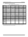
1
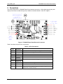
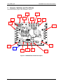
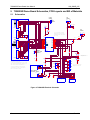
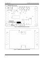
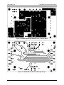
Simplifying System IntegrationTM
73S8009R
Demo Board User Manual
May 7, 2010
Rev. 1.2
UM_8009R_065
73S8009R Demo Board User Manual
UM_8009R_065
© 2010 Teridian Semiconductor Corporation. All rights reserved.
Teridian Semiconductor Corporation is a registered trademark of Teridian Semiconductor Corporation.
Simplifying System Integration is a trademark of Teridian Semiconductor Corporation.
All other trademarks are the property of their respective owners.
Teridian Semiconductor Corporation makes no warranty for the use of its products, other than expressly
contained in the Company’s warranty detailed in the Teridian Semiconductor Corporation standard Terms
and Conditions. The company assumes no responsibility for any errors which may appear in this
document, reserves the right to change devices or specifications detailed herein at any time without
notice and does not make any commitment to update the information contained herein. Accordingly, the
reader is cautioned to verify that this document is current by comparing it to the latest version on
http://www.teridian.com or by checking with your sales representative.
Teridian Semiconductor Corp., 6440 Oak Canyon, Suite 100, Irvine, CA 92618
TEL (714) 508-8800, FAX (714) 508-8877, http://www.teridian.com
2
Rev. 1.2
UM_8009R_065
73S8009R Demo Board User Manual
Table of Contents
1
Introduction ................................................................................................................................... 5
1.1 Package Contents.................................................................................................................... 5
1.2 Safety and ESD Notes ............................................................................................................. 5
1.3 Recommended Operating Conditions and Absolute Maximum Ratings ..................................... 6
2
Connections................................................................................................................................... 7
3
Jumpers, Switches and Test Points ............................................................................................. 9
4
Design Considerations ................................................................................................................ 11
4.1 General Layout Rules ............................................................................................................ 11
4.2 Optimization for Compliance with EMV................................................................................... 11
5
73S8009R Demo Board Schematics, PCB Layouts and Bill of Materials .................................. 12
5.1 Schematics ............................................................................................................................ 12
5.2 73S8009R PCB Layouts ........................................................................................................ 13
5.3 73S8009R Demo Board Bill of Materials................................................................................. 16
6
Ordering Information ................................................................................................................... 17
7
Contact Information..................................................................................................................... 17
Revision History .................................................................................................................................. 18
Rev. 1.2
3
73S8009R Demo Board User Manual
UM_8009R_065
Figures
Figure 1: 73S8009R Demo Board ............................................................................................................ 5
Figure 2: 73S8009R Demo Board External Connectors ............................................................................ 7
Figure 3: 73S8009R Demo Board Description.......................................................................................... 9
Figure 4: 73S8009R Electrical Schematic .............................................................................................. 12
Figure 5: 73S8009R Demo Board: Top View.......................................................................................... 13
Figure 6: 73S8009R Demo Board: Bottom View..................................................................................... 13
Figure 7: 73S8009R Demo Board: Top Signal Layer .............................................................................. 14
Figure 8: 73S8009R Demo Board: Middle Layer 1, Ground Plane .......................................................... 14
Figure 9: 73S8009R Demo Board: Middle Layer 2, Supply Plane ........................................................... 15
Figure 10: 73S8009R Demo Board: Bottom Signal Layer ....................................................................... 15
Tables
Table 1: Recommended Operating Conditions ......................................................................................... 6
Table 2: Absolute Maximum Ratings ........................................................................................................ 6
Table 3: J4 Pin Descriptions .................................................................................................................... 7
Table 4: J2 Pin Descriptions .................................................................................................................... 8
Table 5: 73S8009R Demo Board Description ......................................................................................... 10
Table 6: 73S8009R Demo Board Bill of Materials ................................................................................... 16
Table 7: 73S8009R Demo Board Order Number .................................................................................... 17
4
Rev. 1.2
UM_8009R_065
73S8009R Demo Board User Manual
1 Introduction
The Teridian Semiconductor Corporation 73S8009R Demo Board is a platform for evaluating the Teridian
73S8009R Smart Card Interface IC. It incorporates the 73S8009R integrated circuit and it is designed to
operate either as a standalone platform (to be used in conjunction with an external microcontroller) or as
a daughter card to be used in conjunction with the 73S12xxF evaluation platform.
1.1
Package Contents
Figure 1: 73S8009R Demo Board
The 73S8009R Demo Board Kit includes:
•
•
A 73S8009R Demo Board (Rev. 1)
The following documents:
•
•
1.2
73S8009R Data Sheet
73S8009R Demo Board User Manual (this document)
Safety and ESD Notes
Connecting live voltages to the 73S8009R Demo Board system will result in potentially hazardous
voltages on the boards.
Extreme caution should be taken when handling the 73S8009R Demo Board after
connection to live voltages!
The 73S8009R Demo Board is ESD sensitive! ESD precautions should be taken when
handling this board!
Rev. 1.2
5
73S8009R Demo Board User Manual
1.3
UM_8009R_065
Recommended Operating Conditions and Absolute Maximum Ratings
Table 1: Recommended Operating Conditions
Parameter
Rating
Supply Voltage VDD
2.7 to 3.6 VDC
Supply Voltage VPC
4.75 to 5.5 VDC (ISO-7816 and EMV applications)
4.85 V to 5.5 VDC (NDS applications)
Ambient Operating Temperature
-40 °C to +85 °C
Input Voltage for Digital Inputs
0 V to VDD + 0.3 V
Table 2: Absolute Maximum Ratings
Parameter
Rating
Supply Voltage VDD
-0.5 to 4.0 VDC
Supply Voltage VPC
-0.5 to 6.5 VDC
Input Voltage for Digital Inputs
-0.3 to (VDD+0.5) VDC
Storage Temperature
-60 to 150 °C
Pin Voltage (except card interface)
-0.3 to (VDD+0.5) VDC
Pin Voltage (card interface)
-0.3 to (VCC+0.5) VDC
Pin Current
± 100 mA
ESD Tolerance – Card interface pins
± 6 kV
ESD Tolerance – Other pins
± 2 kV
Operation outside these rating limits may cause permanent damage to the device.
ESD testing on Card pins is HBM condition, 3 pulses, each polarity referenced to ground.
6
Rev. 1.2
UM_8009R_065
73S8009R Demo Board User Manual
2 Connections
This section describes the 73S8009R Demo Board external connectors. All the digital signals and power
supply connections are made through 10-pin header connectors labeled J2 and J4 in Figure 2.
Figure 2: 73S8009R Demo Board External Connectors
Table 3 describes the pins for the J4 connector.
Table 3: J4 Pin Descriptions
Pin
Rev. 1.2
Pin Name
Function
1
RDY
Indicates when smart card power supply is stable and ready.
2
CS
Chip Select – active high.
3
RESET
4
TEST
5
PWRDN
6
CMDVCC%
7
CMDVCC#
8
RSTIN
Controls the card reset signal.
9
GND
Ground.
10
VDD
System interface supply voltage and supply voltage for
companion controller circuitry.
Controls the turn-on, output voltage value, and turn-off of VCC.
7
73S8009R Demo Board User Manual
UM_8009R_065
Table 4 describes the J2 connector pins.
Table 4: J2 Pin Descriptions
Pin
Pin Name
Function
1
SCLK
Clock source input.
2
I/OUC
System controller data I/O to/from the card.
3
AUX1UC
System controller auxiliary data C4 to/from the card.
4
AUX2UC
System controller auxiliary data C8 to/from the card.
5
OFF
Interrupt signal to the processor. Indicator of card presence
and any card fault conditions.
6
GND
Ground.
7
GND
Ground.
8
GND
Ground.
9
VPC IN
Must be between 2.7 V and 6.5 V.
10
VPC IN
Must be between 2.7 V and 6.5 V.
Connections should be made in this order:
• Power Supplies: Apply 3.3 V to pin 10 of J4 or 5 V to pins 9 and 10 of J2 depending on the setting of
JP2.
• Press the ON/OFF button.
• Control signals to the device can be connected through J2 and J4. See Figure 2 and Figure 4.
• Apply the clock signal.
8
Rev. 1.2
UM_8009R_065
73S8009R Demo Board User Manual
3 Jumpers, Switches and Test Points
The items marked in Figure 3 are described in Table 5.
4
6
2
3
5
1
7
8
17
9
10
16
15
14
13
12
11
Figure 3: 73S8009R Demo Board Description
Rev. 1.2
9
73S8009R Demo Board User Manual
UM_8009R_065
Table 5: 73S8009R Demo Board Description
Item #
Schematic &
(Figure 3) PCB Reference
10
Name
Use
1
JP1
Clock selection.
Jumper to select between a clock from 12xx device or
external clock as the frequency reference to the device.
2
JP5
Card Polarity
detect select
13
JP6
The setting of these two jumpers depends on the type
of smart card connector used (whether switch is
nominally open or closed), and which of the card
presence switch input of the 73S8009R is used. In this
demo board, the switch is nominally open. The
jumpers can be set in one of two ways:
1. Default setting: Use of PRES: JP5 must be set to
PRES, and JP6 set to VDD.
2. Alternative use: Use of PRES: JP5 must be set to
PREB, and JP6 set to GND.
3
BNC1
EXTCLK
BNC input for external clock when JP1 is in the
EXTCLK selection (jumper JP1 between terminal 2 and
3).
4
5
6
7
11
12
TP7
TP8
TP5
TP3
TP4
TP6
Test Points:
CLK
C4
RST
VCC
I/O
C8
8
TP9
VDD Select
Two-pin header. Shorting bar jumper must be in place
for normal operation. The shorting jumper can be
replaced with an ammeter to measure the VDD current
to the IC. VDD must be at set with a 3.3V supply.
9
J4
Board 3.3V
supply and
digital control
signals
Connector that gathers the 3.3V supply of the board,
the 73S8009R host control signal pins RDY, CS,
RESET, TEST, PWRDN, CMDVCC%, CMDVCC#, and
RSTIN.
10
J6
Smart Card
Connector
SIM/SAM smart card format connector
Note that J6 is wired in parallel to the smart card
connector J5 (underneath the PCB). No SIM/SAM
should be inserted when using the credit-card size
connector J5.
14
TP2
PWRDN PullDown Selection
Two-pin header. When shorted with a jumper, the
device is in power down mode.
15
J5
Smart Card
Connector
Smart card connector.
When inserting a card (credit card size format),
contacts must face up.
16
TP1
VPC select
Two-pin header. Shorting bar jumper must be in place
for normal operation. The shorting jumper can be
replaced with an ammeter to measure the VPC current
to the IC. VPC must be at set with a 5V supply.
17
J2
Board 5V
supply and host
digital interface
Connector that gathers the 5V supply of the board, the
73S8009R interface IOU, external clock (SCLK) and
interrupt (OFF) pins.
Two-pin test points for each respective smart card
signal. The pin label name is the respective signal (i.e.
VCC, CLK) and the other pin is GND.
Rev. 1.2
UM_8009R_065
73S8009R Demo Board User Manual
4 Design Considerations
4.1
General Layout Rules
Follow these layout rules:
•
•
•
Route I/O and auxiliary signals away from card interface signals.
Keep CLK trace as short as possible and with minimal bends in the trace. If possible, keep routing of
the CLK trace to one layer (avoid vias to other layers). Keep CLK trace away from other traces
especially RST, I/O and VCC. Filtering of the CLK trace is allowed for noise purposes. Up to 30 pF
to ground is allowed at the CLK pin of the smart card connector. Also, the zero Ω series resistor (R7)
can be replaced with a small resistor for additional filtering (no more than 100 Ω).
Keep VCC trace as short as possible. Make trace a minimum of 0.5 mm thick. Also, keep VCC away
from other traces especially RST and CLK.
•
•
•
Keep RST trace away from VCC and CLK traces. Up to 30 pF to ground is allowed for filtering.
Keep 0.1 µF close to VDD pin of the device and directly take other end to ground.
Keep 0.1 µF and 10 µF close to VPC pin of the device and directly take other end to ground.
•
Keep 3.3 µF (1.0 µF for NDS) close to VCC pin of the smart card connector and directly take other
end to ground.
4.2
Optimization for Compliance with EMV
Default configuration of the Demo Board contains a 27 pF capacitor (C12) from the CLK pin of the smart
connector to ground and a 27 pF capacitor (C13) from the RST pin of the smart connector to ground.
These capacitors serve as filters for CLK and RST signals in the case of long traces or test equipment
perturbations. The capacitor on CLK reduces ringing on the trace, reduces coupling to other traces and
slows down the edge of the CLK signal. The capacitor on RST helps the perturbation specification in a
noisy environment. The filter capacitors can be useful in the EMV test environment and have no effect on
NDS testing
C12 and C13 are represented on both schematic and BOM. These capacitors are optional filter
capacitors on the smart card lines CLK and RST, respectively for each card interface. These capacitors
may be adjusted (value, not to exceed 30 pF) or removed to optimize performance in each specific
application (PCB, card clock frequency, compliance with applicable standards etc).
The default VCC capacitor of 3.3 µF is required to meet the dynamic VCC (smart card supply) transient
current requirement in EMV2000 version 4.0.
Rev. 1.2
11
73S8009R Demo Board User Manual
UM_8009R_065
5 73S8009R Demo Board Schematics, PCB Layouts and Bill of Materials
Schematics
CLKIN
SELECT
EXTCLK
5V
C1
10uF
PGND
+
J7
BNC
C2
0.1uF
1
SSM_110_L_SV
2
J2
SCLK
SIO
S_C4
S_C8
INT2
R2
VDD
SELECT
49.9
TP9
C1, C2 and C8 must be placed
within 5mm of the U1 pins and
connected by thick track (wider
than 0.5mm)
5.0V
5V
C3
+
1
2
3
4
5
6
7
8
9
10
5.0V
2
1
1
2
3
1
2
3
4
5
6
7
8
9
10
TP1
SCLK
VPC
SCLK
SIO
SC4
SC8
OFF
GND
GND
GND
+5V
+5V
VPC
SELECT
JP1
J1
10uF
3.3V
U1
VDD
TSM_110_01_L_SV
R4
1
2
3
4
5
6
7
8
9
10
11
12
13
14
J3
RDY
CS
RESET
TEST
PWRDN
CMDVCC5
CMDVCC3
RSTIN
GND
+3.3V
1
2
3
4
5
6
7
8
9
10
SSM_110_L_SV
3.3V
2
1
5.1
CS
RESET
N/C
0FF
I/OUC
AUX1UC
AUX2UC
CMDVCC5
CMDVCC3
RSTIN
CLKIN
RDY
PWRDN
TEST
VDD
GND
PRES
I/O
AUX1
AUX2
VCC
RST
GND
CLK
N/C
N/C
PRES
VPC
28
27
26
25
24
23
22
21
20
19
18
17
16
15
0
C8
0.1uF
J4
USR0
USR1
USR2
USR3
USR4
USR5
USR6
USR7
GND
3.3V
TP2
PWRDN
PULL-DOWN
SELECT
1
2
R7
73S8009R
0
R8
Ru
R9
Ru
R1
These resistors are
not populated
C10
TSM_110_01_L_SV
+
1
2
3
4
5
6
7
8
9
10
10uF
20K
J1 and J3 are placed on the bottom.
are placed on the top side.
R10
Ru
1
2
J2 and J4
TP4
R13
Rd
J1 and J3 must be aligned with J8 and J9 on the
1121 evaluation board (E1121T8) respectivly in
order for this board to be stacked on it.
I/O
1
2
3
J1 must be aligned with J2 and J3 must be
aligned with J4 in order for this daughter
board to be stacked on another.
PRES
C8
1
2
VCC
1
2
RST
TP7
1
2
1
2
TP3 to TP8 to be placed
very close to the pads
of J5
CLK
TP8
PRES
1
2
CARD DETECT
POLARITY SELECT
JP6
R12
Rd
TP5
TP6
JP5
R11
Rd
C11
3.3uF
TP3
C4
GND
1
2
3
VDD
J5
Smart Card Connector
SW2
SW1
C7
C6
C5
C3
C2
C1
C8
I/O
VPP
GND
C4
CLK
RST
VCC
SW-2
SW-1
8
7
6
5
4
3
2
1
8
7
6
5
4
3
2
1
C13
27pF
10
9
C12
27pF
VDD
J6
SIM/SAM Connector
Figure 4: 73S8009R Electrical Schematic
12
Rev. 1.2
UM_8009R_065
5.2
73S8009R Demo Board User Manual
73S8009R PCB Layouts
Figure 5: 73S8009R Demo Board: Top View
Figure 6: 73S8009R Demo Board: Bottom View
Rev. 1.2
13
73S8009R Demo Board User Manual
UM_8009R_065
Figure 7: 73S8009R Demo Board: Top Signal Layer
Figure 8: 73S8009R Demo Board: Middle Layer 1, Ground Plane
14
Rev. 1.2
UM_8009R_065
73S8009R Demo Board User Manual
Figure 9: 73S8009R Demo Board: Middle Layer 2, Supply Plane
Figure 10: 73S8009R Demo Board: Bottom Signal Layer
Rev. 1.2
15
73S8009R Demo Board User Manual
5.3
UM_8009R_065
73S8009R Demo Board Bill of Materials
Table 6: 73S8009R Demo Board Bill of Materials
Qty
Reference
Part
PCB Footprint
Digikey Part
Number
Part Number
Manufacturer
3
C1,C3,C10
10 µF
805
PCC2225CT-ND
ECJ-2FB0J106M
Panasonic
2
C2, C8
0.1 µF
603
PCC1762CT-ND
ECJ-1VB1C104K
Panasonic
1
C11
3.3 µF
805
PCC1925CT-ND
ECJ-2YB0J335K
Panasonic
2
C12, C13
27 pF
603
PCC270ACVCTND
ECJ-1VC1H270J
Panasonic
3
JP1, JP5,
JP6
Header 3
PBC36SAAN
Sullins
2
J1, J3
X
SSM_110_L_SV
Samtec
2
J2, J4
X
TSM_110_01_L_SV
Samtec
1
J5
Smart Card
Connector
ITT_CCM02-2504 CCM02-2504-ND
CCM02-2504
ITTCannon
1
J6
SIM/SAM Connector
ITT_CCM03-3754 CCM03-3754CTND
CCM03-3754
ITTCannon
1
BNC1
BNC Connector
BNC
A24539-ND
414373-1
AMP
2
R4,R7
0
603
P0.0GCT-ND
ERJ-3GEY0R00V
Panasonic
1
R1
20 K
603
P20KGCT-ND
ERJ-3GEYJ203V
Panasonic
1
R2
49.9
603
P49.9HCT
ERJ-3EKF49R0V
Panasonic
3
R8,R9,R10
Ru
603
X
X
3
R11,R12,
R13
Rd
603
X
X
9
TP1,TP2,
TP3,TP4,
TP5,TP6,
TP7,TP8,
TP9
TP2
2X1_Header
S1011-36-ND
PZC36SAAN
Sullins
1
U1
73S8009R
28SOP
X
73S8009R
Teridian
SSM_110_L_SV
3pins, 2.54mm pitch S1011E-36-ND
SSM_110_L_SV
TSM_110_01_L_SV TSM_110_01_L_SV
Note: The resistors noted Ru and Rd in the schematic are not populated on the board. They can be
implemented to adjust the features of the smart card reader.
16
Rev. 1.2
UM_8009R_065
73S8009R Demo Board User Manual
6 Ordering Information
Table 7 lists the order number used to identify the 73S8009R Demo Board.
Table 7: 73S8009R Demo Board Order Number
Part Description
Order Number
73S8009R 28-Pin SO Demo Board
73S8009R-DB
7 Contact Information
For more information about Teridian Semiconductor products or to check the availability of the
73S8009R, contact us at:
6440 Oak Canyon Road
Suite 100
Irvine, CA 92618-5201
Telephone: (714) 508-8800
FAX: (714) 508-8878
Email: [email protected]
For a complete list of worldwide sales offices, go to http://www.teridian.com.
Rev. 1.2
17
73S8009R Demo Board User Manual
UM_8009R_065
Revision History
Revision
Date
Description
1.0
5/22/2007
First publication.
1.1
8/9/2007
Corrected schematic error.
1.2
5/7/2010
Formatted in the new Teridian style.
Added Section 1.1, Package Contents.
Added Section 1.2, Safety and ESD Notes.
Added Table 3: J4 Pin Descriptions.
Added Table 4: J2 Pin Descriptions.
Added Section 7, Ordering Information.
Added Section 9, Contact Information.
Miscellaneous editorial corrections.
18
Rev. 1.2
Mouser Electronics
Authorized Distributor
Click to View Pricing, Inventory, Delivery & Lifecycle Information:
Maxim Integrated:
73S8009R-DB