1
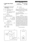
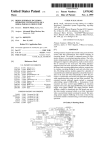
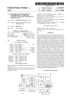
US006185732B1
(12)
(54)
(75)
United States Patent
(10) Patent N0.:
Mann et al.
(45) Date of Patent:
US 6,185,732 B1
Feb. 6, 2001
SOFTWARE DEBUG PORT FOR A
0316609 A3
5/1989 (EP) .
MICROPROCESSOR
0636976 A1
0762279 A1
2/1995 (EP) .
3/1997 (EP) .
Inventors: Daniel P. Mann, Austin, TX (US);
Carl K. Wakeland, Scotts Valley, CA
0849670 A1
59494245
6/1998 (EP) 11/1984 (JP)
OTHER PUBLICATIONS
(US)
(73) Assignee; Advanced Micro Devices, Inc,’
Pentium Processor’s User Manual, vol. 3: Architecture and
Sunnyvale, CA (US)
(*) Notice:
Programming Manual, by Inel Corporation, pp. 17—1
through 17—9, 1994.
Embedded System Engineering Show Catalogue, by
Under 35 USC 154(b), the term of this
patent shall be extended for 0 days.
Motorola, pp. 52—54, Apr./May 1997.
MEVB Quick Start Guide, by Motorola, pp. 3—5 and 7—2
(21) AppL NO‘: 08/923,597
(admitted prior to Aug. 25, 1997).
(22) Filed:
Systems Programming, Aug. 1997.
Choosing a Cross—Debugging Methodology, Embedded
Aug. 25, 1997
CPU 32 Reference Manual, by Motorola, pp. 7—1 through
7—13 (admitted prior to Aug. 25, 1997).
Related U-S- Appheatlen Data
(60)
Provisional application No. 60/043,070, ?led on Apr. 8,
_
1997,
(51)
_
(List contmued on neXt page.)
Int. CI.7 ............................ .. G06F 9/45; G06F 11/34;
Primary Examiner—Kakali Chaki
G06F 11/28
(52)
US. Cl. ................................. .. 717/4; 714/34; 714/38;
(58)
Field of Search .............. .. 395/704, 500.44_500.49;
(74) Attorney, Agent, or Firm—Akin, Gump, Strauss,
Hauer & Feld, LLP
712/227
(57)
A processor-based device incorporating a softWare debug
39, 40, 45, 47, 44, 36; 712/227, 35; 717/4
port that utilizes a JTAG or similar standardized interface,
_
(56)
ABSTRACT
714/25, 27, 30, 31, 32, 33, 34, 35> 38>
thereby providing a softWare debug communication mecha
References Clted
Us‘ PATENT DOCUMENTS
nism that does not require a special bond-out package. In
one embodiment of the invention, only standard JTAG pins
5,058,114
10/1991 Kuboki et al. ....................... .. 714/45
5,491,713 * 2/1996 Samsundaram et al-- 395/ 183-21
are used for communications betWeen a host platform and a
target system incorporating a target processor. In another
embodiment of the invention, the softWare debug port of the
5,544,311 * 8/1996 Hafenbefg et a1~
714/40
target processor is augmented for higher-speed access via
" 712/227
714/45
optional sideband signals. When used in conjunction With an
on-chip trace cache, the softWare debug port provides trace
575607036 : 9/1996
5’724’5O5
3/1998
5,812,562
*
9/1998
714/726
5 838 692 * 11/1998
.
714/724
5:838:897 * 11/1998
.
.
.
.
.
information for reconstructmg instruction execution How on
71460
the processor and is' also capable of enamining register
578617371 *
1/1999 Wi1SCh_Ingang et a1_
510/504
contents Without haltmg processor operation. The softWare
5,862,367 *
5,903,718 *
1/1999 Chiao-Yen ................ .. 710/71
5/1999 Marik ................................... .. 714/38
debug pert alleviates many of the packaging and clock
synchronization problems confronting existing debug solu
tions.
FOREIGN PATENT DOCUMENTS
0316609 A2
5/1989 (EP) .
29 Claims, 4 Drawing Sheets
/202
[104
TR
PROCESSOR
206\
mm:
[208
.?Ié‘Jé‘l‘é;
INTLEJRGFIQCE : V PRCECDEEESDR
Dgg'ggwgn
PROCESSING
—T
210
‘_|'
_’ TRACEIJEBUG
[204
LM§
_.
1
sum
}g|K—-
SDCLK
»TTU——-
212
'NIE‘EFIE“
[218
TRADE
"0mm
/
SERIAL DEBUG
216/
smmn
22o
TRADEPAD
TEST
I
200
INTERFACE
US 6,185,732 B1
Page 2
OTHER PUBLICATIONS
Dec. 1991, pp. 259—261, IBM Technical Disclosure Bulletin,
vol. 34 No. 7B XP000282573.
K5 HDT, e—mail describing K5 HDT, Jan. 11, 1997.
G ff ’R
Advanced
60
Dl
On—chip
Debug for
Cola'Fire Developers,
Embedded Systems Programming, Apr/May 1997, pp. 52
through 54.
IBM Corporation, “Tailorable Embedded Event Trace”,
~11 .ZAd
d O _ h~
D b
f
C 1dF~
evl ’
Vance
n C 1p
6 Hg or
0
He
”EbdddSt
E~
'
A.M
eve opers ’_ m e
1997, pp. 52 54.
* cited by examiner
6
Y5 em
ngmeenng’
pr/ ay
U.S. Patent
1k
Feb. 6, 2001
Sheet 1 0f 4
US 6,185,732 B1
.5 05:
\
H\.
\25¢
. Q2J
El5:a ~2\2:f >5m2a ;
55
E8
2:
E2
m2
U.S. Patent
Feb. 6, 2001
Sheet 3 0f 4
US 6,185,732 B1
[408A
1
TESTCLOCK——-> TCK I
TESTMODESELECT——-—> TMS o
2
o
o
TESTDATAIN—> TDI o
TESTDATAOUT<— mu 0
snuumn
VGND o
9
0
0
0
10
vcc
POWERSUURCE
CMDACK—>COMMANDACKNUWLEDGE
BRTC ———->ENTERDEBUGMDDE,TRACECONTRUL
STOPTX ——>INDEBUGMUDE,RECEIVEDATA
TRIG
<——TRIGGEREVENT
FIG. 3A
/ 108B
TEST CLOCK ——->
TEST MODE SELECT —>
TEST DATA IN —>
TEST DATA DUT 4*“
TEST RESET -——>
TCK
TMS
TDI
TDD
TRST
1
I
O
O
O
O
PDWER SDURCE
VCC Q
CDMMAND ACKNDWILEDGE <— CMDACK I
ENTER DEBUG MDDE, TRACE CDNTRDL —>
BTRC O
IN DEBUG MDDE, RECEIVE DATA 4-- STDPTX O
TRIGGER EVENT <——TRIG D
19
FIG. 3B
2
O
D
O
O
I
VGND
VGND
VGND
VGND
VGND
Q VGND
O VGND
O VGND
Q VGND
O SRESET <—— SYSTEM RESET
20
U.S. Patent
Feb. 6, 2001
Sheet 4 0f 4
US 6,185,732 B1
400
START DEBUG
/ 402
WRITE DEBUG
INSTRUCTION TO
TAP CONTROLLER
I
500
START DEBUG
/404
/ 502
LOADIUNLOAD
38-BIT SERIAL VALUE
WITH PENDING BIT SET
I
WRITE DEBUG
INSTRUCTION TO
TAP CONTROLLER
f 406
LOAD/UNLOAD NEW
38-BIT COMMAND,
CHECK FINISHED FLAG
/ 506
LOADIUNLOAD DEBUG
Y
SCAN CHAIN WITH
PENDING BIT SET
504
CMDACK = I
?
/410
REPEAT LOAD/UNLOAD
OF 38-BIT COMMAND,
CHECK FINISHED FLAG
FIG. 4
FIG. 5
US 6,185,732 B1
1
2
SOFTWARE DEBUG PORT FOR A
MICROPROCESSOR
Where branch activity is high and cache hit rates are loW, it
becomes impossible to hide the BTA-cycles. The resulting
RELATED APPLICATION
“throttle back” to prevent loss of trace information. In the
con?ict over access to the address bus necessitates processor
communications industry, for example, softWare typically
This application claims priority to US. application Ser.
No. 60/043,070, ?led Apr. 8, 1997, Which is hereby incor
makes extensive use of branching and suffers poor cache
utiliZation, often resulting in 20% throttle back or more. This
porated by reference.
amount of throttling is unacceptable amount for embedded
products Which must accommodate real-time constrains.
BACKGROUND OF THE INVENTION
10
1. Field of the Invention
The invention relates to softWare debug support in
microprocessors, and more particularly to a microprocessor
incorporating a softWare debug port.
2. Description of the Related Art
It is clear that the groWth in softWare complexity and
increasing processor clock speeds have placed an increasing
sors operating in-step. Only the main processor is required
15
a slave mode of operation. Free from the need to fetch
developing and debugging neW softWare products has
20
Another existing approach involves building debug sup
port into every processor, but only bonding-out the neces
sary signal pins in a limited number of packages. These
“specially” packaged versions of the processor are used
Within the embedded products industry, Where specialiZed
during debug and replaced With the smaller package for ?nal
on-chip circuitry is often combined With a processor core.
In addition to the softWare engineer, other parties are also
production. This bond-out approach suffers from the need to
support additional bond pad sites in all fabricated devices.
affected by debug tool con?guration. These parties include:
captured trace data that re?ects instruction execution How in
a processor; the in-circuit emulator developer Who deals
This can be a burden in small packages and pad limited
30
and trace bandWidth; and the processor manufacturer Who
cost or design and development complexity.
designs, particularly if a substantial number of “extra” pins
are required by the debug support variant. Additionally, the
debug capability of the specially packaged processors is
With problems of signal synchroniZation, clock frequency
does not Want a solution that results in increased processor
instructions, its address bus and other pins provide the
necessary trace information.
cessor’s failure to adequately facilitate softWare debug
results in longer customer development times and reduces
the processor’s attractiveness for use Within industry. The
need to provide softWare debug support is particularly acute
the “trace” algorithm developer Who must search through
to fetch instructions. The second, slave processor is used to
monitor the fetched instructions on the data bus and keeps its
internal state in synchroniZation With the main processor.
The address bus of the slave processor functions to provide
trace information. After poWer-up, via a JTAG (Joint Test
Action Group) input, the second processor is sWitched into
burden on application softWare developers. The cost of
become a signi?cant factor in processor selection. A pro
In another approach, a second “trace” or “slave” processor
is combined With the main processor, With the tWo proces
35
unavailable in typical processor-based production systems.
In yet another approach (the “Background Debug Mode”
by Motorola, Inc.) limited on-chip debug circuitry is pro
With desktop systems, complex multitasking operating
vided for basic run control. Through a dedicated serial link
systems are currently available to support debugging.
HoWever, the initial task of getting these operating systems
requiring additional pins, this approach alloWs a debugger to
start and stop the target system and apply basic code
running reliably often requires special development equip
40
ment. While not the standard in the desktop environment, the
use of such equipment is often the approach taken Within the
embedded industry. Logic analyZers, read-only memory
(ROM) emulators and in-circuit emulators (ICE) are fre
quently employed. In-circuit emulators do provide certain
45
advantages over other debug environments, offering com
plete control and visibility over memory and register
contents, as Well as overlay and trace memory in case system
memory is insufficient. Use of traditional in-circuit
emulators, Which involves interfacing a custom emulator
50
exacerbated in the future as internal processor clock fre
55
there are a feW knoWn processor manufacturing techniques
Brie?y, a processor-based device according to the present
invention provides a ?exible, high-performance solution for
60
embedded hardWare/softWare debug. Controllability and
observability are achieved through a softWare debug port
that uses an IEEE-1149.1-1990 compliant JTAG (Joint Test
Action Group) interface or a similar standardiZed interface
that is integrated into a processor or processor-based device.
time. In such processors, the address bus is used to report
Target Address). The BTA-cycle, hoWever, must be stolen
from the regular bus operation. In debug environments
quencies continue to increase.
SUMMARY OF THE INVENTION
able to offer the required support for emulation equipment.
Most processors intended for personal computer (PC) sys
tems utiliZe a multiplexed approach in Which existing pins
softWare trace information during a BTA-cycle (Branch
standardiZed interfaces that must be redesigned for each neW
generation of processor. Further, there is currently no
adequate loW-cost procedure for providing trace informa
tion. The limitations of the existing solutions are likely to be
betWeen emulation equipment and the target system, is
are multiplexed for use in softWare debug. This approach is
not particularly desirable in the embedded industry, Where it
is more dif?cult to overload pin functionality.
Other more advanced processors multiplex debug pins in
memory. Once halted, special commands are used to inspect
memory variables and register contents. This serial link,
hoWever, does not provide trace support—additional dedi
cated pins and expensive external capture hardWare are
required to provide trace data.
Thus, the current solutions for softWare debugging suffer
from a variety of limitations, such as increased packaging
and development costs, circuit complexity, processor
throttling, bandWidth matching dif?culties, and non
back-end With a processor socket to alloW communication
becoming increasingly dif?cult and expensive in today’s age
of exotic packages and shrinking product life cycles.
Assuming full-function in-circuit emulation is required,
breakpoints by inserting special instructions in system
65
The softWare debug port provides a serial debug communi
cation mechanism that does not require a special bond-out
package. When used in conjunction With an on-chip trace
US 6,185,732 B1
3
4
cache, the software debug port is capable of providing trace
memory 106. The embedded processor device 102 incorpo
rates a processor core 104 and the debug port 100. Although
not considered critical to the invention, the embedded pro
cessor device 102 may incorporate additional circuitry (not
information for reconstructing instruction execution How on
the processor and is also capable of examining register
contents Without halting processor operation.
shoWn) for performing application speci?c functions, or
Most computers are equipped With a serial or parallel
interface Which can inexpensively be connected to the
softWare debug port of a “target” system by means of a serial
connector to control the debug process. Higher speed
netWork-to-JTAG conversion equipment is also available,
enabling Unix-based Workstations to be easily connected to
the target system. Because a system according to the inven
tion provides a standard debug interface, in-circuit emula
tion equipment designed to interface With the physical
may take the form of a stand-alone processor or digital
signal processor. Preferably, the debug port 100 uses an
IEEE-1149.1- 1990 compliant JTAG interface or other simi
10
lar standardiZed serial port interface.
Ahost system H is used to execute debug control softWare
112 for transferring high-level commands and controlling
the extraction and analysis of debug information generated
by the target system T. The host system H and target system
host platform and a target system incorporating the target
T of the disclosed embodiment of the invention communi
cate via a serial link 110. Most computers are equipped With
a serial or parallel interface Which can be inexpensively
connected to the debug port 100 by means of a serial
connector 108, alloWing most computers to function as a
host system H. Exemplary serial connectors 108 are
described beloW in conjunction With FIGS. 3A and 3B.
processor. In another embodiment according to the
Alternatively, the serial connector 108 could be replaced
connector can be reused Without the need to develop expen
sive back-end equipment to conform With variations and
advances in processor packaging.
In one embodiment according to the invention, only
15
standard J TAG pins are used for communications betWeen a
invention, the softWare debug port of the target processor is
augmented for higher-speed access via optional sideband
signals. These optional sideband signals can also be used
With higher speed JTAG-to-netWork conversion equipment.
Referring noW to FIG. 2, details of the embedded pro
cessor device 102 are provided. In addition to the processor
core 104, FIG. 2 depicts the various elements of an enhanced
With a bond-out parallel interface that provides even greater
functionality. A custom command set provides effective
embodiment of the debug port 100. At a minimum, only the
conventional JTAG pins need be supported in the softWare
debug port 100 according to the invention. The JTAG pins
controllability and observability for the debug solution.
These commands operate in conjunction With a plurality of
internal debug registers to pass trace, status and control
information to and from on-chip debug and trace logic.
essentially become a transportation mechanism, using exist
ing pins, to enter commands to be performed by the pro
When used With an on-chip trace cache, no external capture
hardWare is required in order to receive trace information.
Thus, a processor or processor-based product according to
cessor core 104. Assuming that the embedded processor
the invention incorporates a softWare debug port providing
a loW cost, loW intrusion communication channel betWeen a 35
target system and a host platform. The softWare debug port
alleviates many of the packaging and clock synchroniZation
problems that limit existing debug solutions.
device 102 already supports JTAG functionality, only four
pins are required in the non-bondout package to fully
support the 10-pin debug port 100 format of FIG. 3A.
More speci?cally, the test clock signal TCK, the test mode
select signal TMS, the test data input signal TDI and the test
data output signal TDO provided to and driven by the JTAG
Test Access Port (TAP) controller 204 are conventional
JTAG support signals and knoWn to those skilled in the art.
BRIEF DESCRIPTION OF THE DRAWINGS
As discussed in more detail beloW, an enhanced embodiment
A better understanding of the present invention can be
of the debug port 100 adds the command acknoWledge
obtained When the folloWing detailed description of the
preferred embodiment is considered in conjunction With the
signal CMDACK, the break request/trace capture signal
BRTC, the stop transmit signal STOPTX, and the trigger
folloWing draWings, in Which:
FIG. 1 is a block diagram of a softWare debug environ
signal TRIG to the standard JTAG interface. The additional
45
ment utiliZing a softWare debug port according to the present
signals alloW for pinpoint accuracy of external breakpoint
assertion and monitoring, triggering of external devices in
response to internal breakpoints, and elimination of status
invention;
polling of the JTAG serial interface. Although these “side
band” signals offer extra functionality and improve commu
nications speeds for the debug port 100, they are not
required in the simplest embodiment of the invention (using
FIG. 2 is a block diagram providing details of an exem
plary embedded processor product incorporating a softWare
debug port according to the present invention;
FIGS. 3A and 3B depict exemplary softWare debug port
only the conventional JTAG support signals). These signals
connectors for use in a debug environment in accordance
With the invention;
FIG. 4 is a ?oWchart illustrating softWare debug port
are used, hoWever, With an optional parallel port 214 pro
vided on special bond-out versions of the embedded pro
55 cessor device 102.
command passing according to one embodiment of the
Via the conventional JTAG signals, the JTAG TAP con
troller 204 accepts standard JTAG serial data and control.
invention; and
FIG. 5 is a ?oWchart illustrating enhanced softWare debug
port command passing according to a second embodiment of
the invention.
When a DEBUG instruction has been Written to the JTAG
instruction register, a serial debug shifter 212 is connected to
the JTAG test data input signal TDI and test data output
signal TDO, such that commands and data can then be
loaded into and read from debug registers 210. In the
DETAILED DESCRIPTION OF THE
PREFERRED EMBODIMENT
Turning noW to the draWings, FIG. 1 depicts a softWare
debug environment utiliZing a debug port 100 according to
the present invention. A target system T is shoWn containing
an embedded processor device 102 coupled to system
65
disclosed embodiment of the invention, the debug registers
210 include tWo debug registers for transmitting (TXi
DATA register) and receiving (RXiDATA register) data, an
instruction trace con?guration register (ITCR), and a debug
control status register (DCSR).
US 6,185,732 B1
6
5
406 Where the pending command is loaded/unloaded and the
command ?nished ?ag checked. Completion of a command
A control interface state machine 206 coordinates the
loading/reading of data to/from the serial debug shifter 212
and the debug registers 210. A command decode and pro
cessing block 208 decodes commands/data and dispatches
them to processor interface logic 202 and trace debug
typically involves transferring a value betWeen a data reg
ister and a processor register or memory/IO location. After
the command has been completed, the processor 104 clears
interface logic 216. The processor interface logic 202 com
the command pending ?ag and sets the command ?nished
municates directly With the processor core 104, as Well as
?ag, at the same time storing a value in the data ?eld if
trace control logic 218. Parallel port logic 214 communi
applicable. The entire 38-bit register is scanned to monitor
the command ?nished and command pending ?ags. If the
cates With a control interface state machine 206 and the
debug registers 210 to perform parallel data read/Write
10
operations in optional bond-out versions of the embedded
the previous command has ?nished. The status of the ?ags
is captured by the control interface state machine 206. A
slave copy of the ?ags’ status is saved internally to deter
processor device 102.
The trace control circuitry 218 provides trace information
for reconstructing instruction execution How on the proces
sor core 104. The trace control circuitry 218 supports tracing
15
either to a port 204 or 214 or to the internal trace cache 200
and provides user control for selectively turning trace on and
off. Other features enabled by the trace control circuitry 218
include programmability of synchroniZation address genera
tion and user speci?ed trace records. The trace control 218
circuitry also controls the trace pad interface port 220. When
utiliZed, the trace pad interface port 220 is capable of
providing trace data While the processor core 104 is execut
ing instructions, although clock synchroniZation and other
25
dif?culties may arise.
pending ?ag is reset to Zero and the ?nished ?ag is set to one,
mine if the neXt instruction should be loaded. The slave copy
is maintained due to the possibility of a change in ?ag status
betWeen TAP controller 204 states. This alloWs the processor
104 to determine if the previous instruction has ?nished
before loading the neXt instruction.
If the ?nished ?ag is not set as determined in step 408,
control proceeds to step 410 and the loading/unloading of
the 38-bit command is repeated. The command ?nished ?ag
is also checked. Control then returns to step 408. If the
?nished ?ag is set as determined in step 408, control returns
to step 406 for processing of the neXt command. DEBUG
mode is eXited via a typical JTAG process.
Returning to FIG. 2, the aforementioned optional side
The trace cache 200 improves bandWidth matching and
reduces the need to incorporate throttle-back circuitry in the
band signals are utiliZed in the enhanced debug port 100 to
processor core 104. In one contemplated embodiment of the
provide eXtra functionality. The optional sideband signals
invention, the trace cache 200 is a 128 entry ?rst-in, ?rst-out
(FIFO) circular cache. Increasing the siZe of the trace cache
200 Would lengthen the amount of softWare trace informa
tion that can be capture.
include a break request/trace capture signal BRTC that can
Before debug information is communicated via the debug
port 100 using only conventional J TAG signals, the port 100
is enabled by Writing the public JTAG instruction DEBUG
function as a break request signal or a trace capture enable
signal depending on the status of bit set in the debug
control/status register. If the break request/trace capture
signal BRTC is set to function as a break request signal, it
is asserted to cause the processor 104 to enter debug mode
35
into a JTAG instruction register contained Within the TAP
controller 204. As shoWn beloW, the JTAG instruction reg
ister of the disclosed embodiment is a 38-bit register com
prising a 32-bit data ?eld (debugidata[31:0]), a four-bit
command ?eld to point to various internal registers and
(the processor 104 can also be stopped by scanning in a halt
command via the convention JTAG signals). If set to func
tion as a trace capture enable signal, asserting the break
request/trace capture signal BRTC enables trace capture.
Deasserting the signal turns trace capture off. The signal
takes effect on the neXt instruction boundary after it is
functions provided by the debug port 100, a command
pending ?ag, and a command ?nished ?ag. It is possible for
detected and is synchroniZed With the internal processor
clock. The break request/trace capture signal BRTC may be
some commands to use bits from the debugidata ?eld as a
asserted at any time.
sub-?eld ?eld to eXtend the number of available commands.
37
5
debugidata
2
1
45
O
command I P I F I
JTAG Instruction Register
This JTAG instruction register is selected by toggling the
test mode select signal TMS. The test mode select signal
TMS alloWs the JTAG path of clocking to be changed in the
55
scan path, enabling multiple paths of varying lengths to be
used. Preferably, the JTAG instruction register is accessible
via a short path. This register is con?gured to include a
“soft” register for holding values to be loaded into or
The trigger signal TRIG is con?gured to pulse Whenever
an internal processor breakpoint has been asserted. The
trigger signal TRIG may be used to trigger an eXternal
capturing device such as a logic analyZer, and is synchro
niZed With the trace record capture clock signal TRACE
CLK. When a breakpoint is generated, the event is synchro
niZed With the trace capture clock signal TRACECLK, after
Which the trigger signal TRIG is held active for the duration
of trace capture.
The stop transmit signal STOPTX is asserted When the
processor 104 has entered DEBUG mode and is ready for
register interrogation/modi?cation, memory or I/O reads and
Writes through the debug port 100. In the disclosed embodi
ment of the invention, the stop transmit signal STOPTX
re?ects the state of a bit in the debug control status register
received from speci?ed system registers.
(DCSR). The stop transmit signal STOPTX is synchronous
FIG. 4 provides a high-level ?oW chart of command
passing When using a standard JTAG interface. Upon enter
ing debug mode in step 400 the DEBUG instruction is
Written to the TAP controller 204 in step 402. Next, step 404,
With the trace capture clock signal TRACECLK.
the 38-bit serial value is shifted in as a Whole, With the 65
The command acknoWledge signal CMDACK is
described in conjunction With FIG. 5, Which shoWs simpli
?ed command passing in the enhanced debug port 100 of
FIG. 2. Again, to place the target system T into DEBUG
command pending ?ag set and desired data (if applicable,
mode, a DEBUG instruction is Written to the TAP controller
otherWise Zero) in the data ?eld. Control proceeds to step
204 in step 502. Control proceeds to step 504 and the
US 6,185,732 B1
8
7
Instruction Trace Con?guration Register (ITCR)
Another debug register, the debug control/status register
command acknowledge signal CMDACK is monitored by
the host system H to determine command completion status.
This signal is asserted high by the target system T simulta
neously with the command ?nished ?ag and remains high
until the next shift cycle begins. When using the command
(DCSR), provides an indication of when the processor 104
has entered debug mode and allows the processor 104 to be
forced into DEBUG mode through the enhanced JTAG
interface. As shown in the following table, the DCSR also
acknowledge signal CMDACK, it is not necessary to shift
out the JTAG instruction register to capture the command
enables miscellaneous control features, such as: forcing a
?nished ?ag status. The command acknowledge signal
CMDACK transitions high on the next rising edge of the test
clock signal TCK after the command ?nished ?ag has
changed from Zero to one. When using the enhanced JTAG
signals, a new shift sequence (step 506) is not started by the
host system H until the command acknowledge signal
CMDACK pin has been asserted high. The command
acknowledge signal CMDACK is synchronous with the test
ready signal to the processor 104, controlling memory
10
access space for accesses initiated through the debug port,
disabling cache ?ush on entry to the DEBUG mode, the TX
and RX bits, the parallel port 214 enable, forced breaks,
forced global reset, and other functions. The ordering of bits
in either the ITCR or DCSR is not considered critical to the
invention.
15
clock signal TCK. The test clock signal TCK need not be
clocked at all times, but is ideally clocked continuously
when waiting for a command acknowledge signal
CMDACK response.
OPERATING SYSTEM/APPLICATION COMMUNICA
TION VIA THE DEBUG PORT 100
BIT
SYMBOL
31:12
11
Reserved
Reserved
TX
Indicates that the target system T is ready to
10
RX
transmit data to the host system H and the data
Also included in debug register block 210 is an instruction
is available in the TXiDATA register
trace con?guration register (ITCR). This 32-bit register
provides for the enabling/disabling and con?guration of
instruction trace debug functions. Numerous such functions
are contemplated, including various levels of tracing, trace
25
8
DISFLUSH
SMMSP
7
STOP
6
FRCRDY
5
SYMBOL
DESCRIPTION/FUNCT ION
31:30
29
28
Reserved
RXINTEN
TXINTEN
Reserved
Enables interrupt when RX bit is set
Enables interrupt when TX bit is set
27
TX
4
26
RX
Indicates that the target system T is ready to
transmit data to the host system H and the data
is available in the TXiDATA register
Indicates that data has been received from the
25
24
DISL1TR
DISLOTR
Disables level 1 tracing
Disables level 0 tracing
Forces the ready signal RDY to the processor
104 to be pulsed for one processor clock;
useful when it is apparent that the processor
104 is stalled waiting for a ready signal
from a non-responding device
BRKMODE Selects the function of the break request/
trace capture signal BRTC (break request or
23
DISCSB
Disables current segment base trace record
22:16
TSYNC[6:O] Sets the maximum number of Branch Sequence
trace records that may be output by the
DBTEN
registers DRO-DR7 or other legacy debug
2
PARENB
DSPC
trap/fault mechanisms
Enables parallel port 214
Disables stopping of internal processor
1
FBRK
clocks in the Halt and Stop Grant states
Forces processor 104 into DEBUG mode at the
next instruction boundary (equivalent to
pulsing the external BRTC pin)
O
FRESET
Forces global reset
45
Debug Control/Status Register (DCSR)
trace control block 218 before a synchronizing
address record is forced
When in cross debug environment such as that of FIG. 1,
it is necessary for the parent task running on the target
system T to send information to the host platform H con
15
14
13
12
TSR3
TSR2
TSR1
TSRO
Sets
Sets
Sets
Sets
11
1O
9
8
TRACE3
TRACE2
TRACE1
TRACEO
Enables
Enables
Enables
Enables
7
6:4
TRON
TCLK[2:O]
data in a known region, then via a trap instruction, cause
DEBUG mode to be entered.
3
ITM
Trace on/off
Encoded divider ratio between internal
processor clock and TRACECLK
Sets internal or external (bond-out) instruction
tracing mode
then determine the reason that UG mode was entered, and
2
TINIT
1
TRIGEN
Trace
Trace
Trace
Trace
mode
mode
mode
mode
DR3
DR2
DR1
DRO
Enables entry to debug mode or toggle trace
mode enable on a trap/fault via processor 104
host and placed in the RXiDATA register
on
on
on
on
accesses initiated through the Debug Port 100
Indicates whether the processor 104 is in
DEBUG mode (equivalent to stop transmit
trace capture on/off)
BH‘
mode
mode
mode
mode
Controls memory access space (normal memory
signal STOPTX
35
trace
trace
trace
trace
Disables cache ?ush on entry to DEBUG mode
space/system management mode memory) for
tracing modes, clock divider ratio information, as well as
additional functions shown in the following table. The ITCR
is accessed through a JTAG instruction register write/read
command as is the case with the other registers of the debug
register block 210, or via a reserved instruction.
clears
clears
clears
clears
Indicates that data has been received from the
host and placed in the RXiDATA register
synchroniZation force counts, trace initialiZation, instruction
or
or
or
or
DESCRIPTION/FUNCTION
toggling
toggling
toggling
toggling
trap
trap
trap
trap
using
using
using
using
DR3
DR2
DR1
DRO
trolling it. This data may consist, for example, of a character
stream from a printf call or register information from a
55
Via debug port 100 commands, the host system H can
Trace initialization
respond by retrieving the data from the reserved region.
Enables pulsing of external trigger signal
However, while the processor 104 is in DEBUG mode,
normal processor execution is stopped. As noted above, this
is undesirable for many real-time systems.
This situation is addressed according to the present inven
TRIG following receipt of any legacy debug
breakpoint; independent of the Debug Trap
Enable function in the DCSR
O
GTEN
Global enable for instruction tracing through
the internal trace buffer or via the external
(bond-out) interface
Task’s Control Block (TCB). One contemplated method for
transferring the data is for the operating system to place the
65
tion by providing two debug registers in the debug registers
210 for transmitting (TXiDATA register) and receiving
(RXiDATA register) data. These registers can be accessed
US 6,185,732 B1
9
10
using the soft address and JTAG instruction register com
mands. As noted, after the host system H has Written a debug
instruction to the JTAG instruction register, the serial debug
shifter 212 is coupled to the test data input signal TDI line
and test data output signal TDO line.
When the processor 104 executes code causing it to
or enhanced) are used for debug access to the target system
T When the processor 104 is executing instructions.
In a similar manner to the J TAG standard, all inputs to the
transmit data, it ?rst tests a TX bit in the ITCR. If the TX bit
parallel port 214 are sampled on the rising edge of the test
clock signal TCK, and all outputs are changed on the falling
edge of the test clock signal TCK. In the disclosed
embodiment, the parallel port 214 shares pins With the trace
is set to Zero then the processor 104 executes a processor
pad interface 220, requiring parallel commands to be initi
instruction (either a memory or I/ O Write) to transfer the data
to the TXiDATA register. The debug port 100 sets the TX
bit in the DCSR and ITCR, indicating to the host system H
that it is ready to transmit data. Also, the STOPTX pin is set
10
ated only While the processor 104 is stopped and the trace
pad interface 220 is disconnected from the shared bus.
The parallel bus request signal PBREQ and parallel bus
grant signal PBGNT are provided to expedite multiplexing
high. After the host system H completes reading the transmit
of the shared bus signals betWeen the trace cache 200 and the
data from the TXiDATA register, the TX bit is set to Zero.
ATXINTEN bit in the ITCR is then set to generate a signal
parallel port 214. When the host interface to the parallel port
214 determines that the parallel bus request signal PBREQ
15
to interrupt the processor 104. The interrupt is generated
is asserted, it begins driving the parallel port 214 signals and
only When the TX bit in the ITCR transitions to Zero. When
the TXINTEN bit is not set, the processor 104 polls the
ITCR to determine the status of the TX bit to further transmit
data.
When the host system H desires to send data, it ?rst tests
a RX bit in the ITCR. If the RX bit is set to Zero, the host
asserts the parallel bus grant signal PBGNT.
When entering or leaving DEBUG mode With the parallel
port 214 enabled, the parallel port 214 is used for the
processor state save and restore cycles. The parallel bus
request signal PBREQ is asserted immediately before the
beginning of a save state sequence penultimate to entry of
system H Writes the data to the RXiDATA register and the
DEBUG mode. On the last restore state cycle, the parallel
RX bit is set to one in both the DCSR and ITCR. A RXINT
bus request signal PBREQ is deasserted after latching the
Write data. The parallel port 214 host interface responds to
bit is then set in the ITCR to generate a signal to interrupt
25
the processor 104. This interrupt is only generated When the
parallel bus request signal PBREQ deassertion by tri-stating
RX in the ITCR transitions to one. When the RXINTEN bit
status of the RX bit. If the RX bit is set to one, the processor
instruction is executed to read data from the RXiDATA
its parallel port drivers and deasserting the parallel bus grant
signal PBGNT. The parallel port 214 then enables the debug
trace port pin drivers, completes the last restore state cycle,
asserts the command acknowledge signal CMDACK, and
register. After the data is read by the processor 104 from the
returns control of the interface to trace control logic 218.
is not set, the processor 104 polls the ITCR to verify the
RXiDATA register the RX bit is set to Zero. The host
When communicating via the parallel port 214, the
system H continuously reads the ITCR to determine the
address pins PADR[2:0] are used for selection of the ?eld of
the JTAG instruction register, Which is mapped to the 16-bit
data bus PDATA[15:0]. It is not necessary to update both
halves of the debug data [31:0] register if only one of the
halves is being used (e.g., on 8-bit I/O cycle data Writes).
The command pending ?ag is automatically set When per
forming a Write operation to the four-bit command register,
and is cleared When the command ?nished ?ag is asserted.
status of the RX bit to further send data.
This technique enables an operating system or application
to communicate With the host system H Without stopping
processor 104 execution. Communication is conveniently
achieved via the debug port 100 With minimal impact to
35
on-chip application resources. In some cases it is necessary
to disable system interrupts. This requires that the RX and
TX bits be examined by the processor 104. In this situation,
The host system H can monitor the command acknowledge
signal CMDACK to determine When the ?nished ?ag has
the communication link is driven in a polled mode.
PARALLEL INTERFACE TO DEBUG PORT 100
Some embedded systems require instruction trace to be
examined While maintaining I/O and data processing opera
been asserted. Use of the parallel port 214 provides full
45
tions. Without the use of a multi-tasking operating system,
a bond-out version of the embedded processor device 102 is
preferable to provide the trace data, as examining the trace
sor core 104.
OPERATING SYSTEM AND DEBUGGER INTEGRA
TION
The operation of all debug supporting features, including
cache 102 via the debug port 100 requires the processor 104
to be stopped.
In the disclosed embodiment of the invention, a parallel
port 214 is also provided in an optional bond-out version of
the embedded processor device 102 to provide parallel
the trace cache 200, can be controlled through the debug port
100 or via processor instructions. These processor instruc
tions may be from a monitor program, target hosted
debugger, or conventional pod-Wear. The debug port 100
access to the debug port 100. This interface provides a 16-bit
data path that is multiplexed With the trace pad interface port
220. More speci?cally, the parallel port 214 provides a
16-bit Wide bi-directional data bus (PDATA[15 10]), a 2-bit
address bus (PADR[2:0]), a read/Write strobe signal (PRW),
visibility of execution history, even When the trace cache
200 is turned on, Without requiring throttling of the proces
55
performs data moves Which are initiated by serial data port
commands rather than processor instructions.
Operation of the processor from conventional pod-space
is very similar to operating in DEBUG mode from a monitor
program. All debug operations can be controlled via pro
and a request—grant signal pair PBREQ-PBGNT (not
shoWn). The parallel port 214 is enabled by setting a bit in
the DCSR. Serial communications via the debug port 100
instructions come from pod-space or regular memory. This
enables an operating system to be extended to include
are not disabled When the parallel port 214 is enabled.
additional debug capabilities.
The parallel port 214 is primarily intended for fast
doWnloads/uploads to and from target system T memory.
HoWever, the parallel port 214 may be used for all debug
communications With the target system T Whenever the
processor 104 is stopped. The serial debug signals (standard
cessor instructions. It makes no difference Whether these
Of course, via privileged system calls such a ptrace,
operating systems have long supported debuggers. HoWever,
65
the incorporation of an on-chip trace cache 200 noW enables
an operating system to offer a trace capability. The ability to
trace is often considered essential in real-time applications.
US 6,185,732 B1
11
12
In a debug environment according to the present invention,
an operating system could support limited trace Without the
incorporation of an “external” logic analyZer or in-circuit
emulator.
Extending an operating system to support on-chip trace
has certain advantages Within the communications industry.
It enables the system I/O and communication activity to be
maintained While a task is being traced. Traditionally, the
Which the target address is provided from a data register or
other memory location such as a stack.
As indicated in the preceding table, other desired trace
information includes: the target address of a trap or interrupt
handler; the target address of a return instruction; a condi
tional branch instruction having a target address Which is
data register dependent (otherWise, all that is needed is a
use of an in-circuit emulator has necessitated that the
processor be stopped before the processor’s state and trace
10
can be examined [unlike ptrace()]. This disrupts continuous
support of 1/0 data processing. The trace cache 200 is very
start information, can also be placed in the trace cache 200.
The precise contents and nature of the trace records are not
considered critical to the invention.
useful When used With equipment in the ?eld. If an unex
pected system crash occurs, the trace cache 200 can be
examined to observe the execution history leading up to the
crash event. When used in portable systems or other envi
1-bit trace indicating if the branch Was taken or not); and,
most frequently, addresses from procedure returns. Other
information, such as task identi?ers and trace capture stop/
FIGS. 3A and 3B depict exemplary serial debug port
15
connectors 108A and 108B, respectively, for use in a debug
environment according to the invention. Referring ?rst to
FIG. 3A, the communication signals of the enhanced version
ronments in Which poWer consumption is a concern, the
of the debug port 100 are provided as shoWn to a 10-pin
serial connector 108A. A poWer supply signal Vcc and a
trace cache 200 can be disabled as necessary via poWer
management circuitry.
TRACE RECORD FORMAT
In the disclosed embodiment of the invention, an instruc
tion trace record (ITREC) is 20 bits Wide and consists of tWo
?elds, TCODE and TDATA. The TCODE ?eld is a code that
identi?es the type of data in the TDATA ?eld. The TDATA
20
?eld contains softWare trace information used for debug
25
ground signal Vgnd are also coupled to the serial connector
108A. By providing the serial connector 108A in production
systems, a host system H can be readily coupled, thereby
facilitating in-?eld debugging operations.
purposes.
Referring noW to FIG. 3B, a 20-pin serial connector 108B
is shoWn. This version of the serial connector 108 is pre
ferred in situations in Which the serial connector is clocked
at high speeds (e.g., above 10 MHZ) Where there is a danger
of signal cross-talk. Although the signals of the connector
19
108A of FIG. 3A are identical to those of FIG. 3B, the 20-pin
TCODE
TDATA
30
arrangement places a ground Wire betWeen each signal Wire
to reduce signal cross-talk. It should be noted that voltage
level conversion may be required in the serial connector
108A or 108B to ensure correct voltage levels for connecting
Instruction Trace Record Format
a host system H or other interface. The precise ordering of
In one contemplated embodiment of the invention, the
embedded processor device 102 reports eleven different
the debug port 100 signals provided by the serial connectors
trace codes as set forth in the folloWing table:
Thus, a processor-based device providing a ?exible, high
performance solution for embedded hardWare/softWare
debug has been described. The processor-based device
TCODE# TCODE Type
TDATA
0000
Missed Trace
Not valid
0001
0010
0011
Conditional Branch
Branch Target
Previous Segment
Contains Branch Sequence
Contains Branch Target Address
Contains Previous Segment Base
Base
Address and Attributes
0100
0101
108A and 108B is not considered critical to the invention.
40
communication mechanism that does not require a special
bond-out package. When used in conjunction With an
45
Current Segment Base Contains Current Segment Base
Address and Attributes
Interrupt
Contains Vector Number of
0111
Trace Synchronization Contains Address or Currently
Executed Instruction
Multiple Trace
Contains 2nd or 3rd Record
1000
Trace Stop
User Trace
Performance Pro?le
execution How on the processor and is also capable of
clock synchroniZation problems.
50
of Entry With Multiple Records
1001
1010
on-chip trace cache, the softWare debug port is capable of
providing trace information for reconstructing instruction
examining register contents Without halting processor opera
tion. The softWare debug port alleviates many packaging and
Exception or Interrupt
0110
incorporates a softWare debug port that utiliZes a JTAG or
similar standardiZed interface, providing a serial debug
The foregoing disclosure and description of the invention
are illustrative and explanatory thereof, and various changes
Contains Instruction Address
in the siZe, shape, materials, components, circuit elements,
Where Trace Capture Was Stopped
Wiring connections and contacts, as Well as in the details of
Contains User Speci?ed Trace Data
Contains Performance Pro?ling Data
55
the invention.
What is claimed is:
The trace cache 200 is of limited storage capacity; thus a
certain amount of “compression” in captured trace data is
1. Aprocessor-based device provided With pins to permit
connection to external electrical devices, the processor
desirable. In capturing trace data, the folloWing discussion
assumes that an image of the program being traced is
the illustrated circuitry and construction and method of
operation may be made Without departing from the spirit of
60
based device comprising:
available to the host system H. If an address can be obtained
a processor core;
from a program image (Object Module), then it is not
provided in the trace data. Preferably, only instructions
Which disrupt the instruction How are reported; and further,
only those Where the target address is in some Way data
dependant. For example, such “disrupting” events include
a serial port formed of a plurality of pins con?gured to
receive standardiZed serial port signals as Well as
call instructions or unconditional branch instructions in
signals from external non-trace capture softWare deDug
equipment;
control circuitry coupled to the serial port for decoding
and differentiating betWeen standardiZed serial port
US 6,185,732 B1
14
13
signals and signals used by the external non-trace
10. The softWare debug platform of claim 9, Wherein the
serial port is essentially compliant With the IEEE-1149.1
capture software debug equipment;
1990 JTAG interface standard or other similar standard.
a plurality of debug registers coupled to the control
circuitry and the processor core for receiving and
providing debug data and control signals; and
11. The processor-based device of claim 10, Wherein the
serial port utiliZes the conventional JTAG signals TMS,
TCK, TDI and TDD.
12. The softWare debug platform of claim 9, Wherein the
at least one additional pin of the serial port con?gured to
facilitate communication betWeen the external non
status of the at least one additional pin is capable of being
trace capture softWare debug equipment and the pro
examined by the host system Without halting normal pro
cessor core,
Wherein the processor core is adapted to perform various
10
softWare debug operations in response to signals from
the external non-trace capture softWare debug
equipment, the at least one additional pin providing an
indication of the status of select softWare debug opera
tions.
2. The processor-based device of claim 1, Wherein the
serial port is essentially compliant With the IEEE-1149.1
13. The softWare debug platform of claim 9, further
comprising an on-chip trace cache coupled to the processor
core and serial port, the trace cache adapted to store infor
mation indicative of the order in Which instructions are
executed by the processor core.
15
14. The softWare debug platform of claim 13, Wherein the
contents of the trace cache can be examined by the host
system via the serial port.
15. The softWare debug platform of claim 9, Wherein the
debug connector is a serial-to-parallel interface.
16. The softWare debug platform of claim 9, Wherein the
1990 JTAG interface standard or other similar standard.
3. The processor-based device of claim 1, Wherein the
serial port utiliZes the conventional JTAG signals TMS,
TCK, TDI and TDD.
4. The processor-based device of claim 1, Wherein the
status of the at least one additional pin is capable of being
debug connector is a serial-to-netWork interface.
17. The softWare debug platform of claim 9, Wherein the
indication of the status of select softWare debug operations
examined by external softWare debug equipment Without
halting normal processor operation.
5. The processor-based device of claim 1, further com
prising an on-chip trace cache coupled to the processor core
and serial port, the trace cache adapted to store information
indicative of the order in Which instructions are executed by
cessor core operation.
comprises assertion of a signal at the at least one additional
25
pin folloWing completion of a debug operation.
18. The softWare debug platform of claim 9, Wherein the
indication of the status of select softWare debug operations
comprises assertion of a signal at the at least one additional
the processor core.
contents of the trace cache can be examined by external
pin folloWing receipt of a debug data or control signal.
19. Aprocessor-based device provided With pins to permit
softWare debug equipment via the serial port.
7. The processor-based device of claim 1, Wherein the
based device comprising:
6. The processor-based device of claim 5, Wherein the
connection to external electrical devices, the processor
indication of the status of select softWare debug operations
comprises assertion of a signal at the at least one additional
pin folloWing completion of a debug operation.
a processor core;
35
8. The processor-based device of claim 1, Wherein the
indication of the status of select softWare debug operations
signals from external non-trace capture softWare debug
equipment;
comprises assertion of a signal at the at least one additional
at least one additional pin con?gured to facilitate com
munication betWeen external non-trace capture soft
pin folloWing receipt of a debug data or control signal.
9. A softWare debug platform for communicating With a
non-trace capture host system capable of executing debug
softWare that controls the extraction and analysis of debug
Ware debug equipment and the processor core;
control means coupled to the serial port for decoding and
differentiating betWeen standardiZed serial port signals
and signals used by external non-trace capture softWare
information, the softWare debug platform comprising:
a target system having a processor-based device, the
processor-based device comprising:
45
the processor core for receiving and providing debug
data and control signals,
a serial port formed of a plurality of pins con?gured to
receive standardiZed serial port signals as Well as
signals from the non-trace capture host system;
Wherein the processor core is adapted to perform various
control circuitry coupled to the serial port for decoding
and differentiating betWeen standardiZed serial port
signals and signals used by the non-trace capture
host system;
a plurality of debug registers coupled to the control
softWare debug operations in response to signals from
external non-trace capture softWare debug equipment,
the at least one additional pin providing an indication of
the status of softWare debug operations.
20. The processor-based device of claim 19, further
55
providing debug data and control signals; and
to facilitate communication betWeen non-trace cap
ture host system and the processor core,
21. The processor-based device of claim 20, Wherein the
Wherein the processor core is adapted to perform vari
ous softWare debug operations in response to signals
from the non-trace capture host system, the at least
one additional pin providing an indication of the
serial port and the at least one additional pin of the
target system With the non-trace capture host system.
comprising trace storage means coupled to the processor
core and serial port, the trace storage means adapted to store
information indicative of the order in Which instructions are
executed by the processor core.
at least one additional pin of the serial port con?gured
status of select softWare debug operations; and
a debug connector for communicatively coupling the
debug equipment; and
communication means coupled to the control means and
a processor core;
circuitry and the processor core for receiving and
a serial port formed of a plurality of pins con?gured to
receive standardiZed serial port signals as Well as
contents of the trace storage means can be examined by
external softWare debug equipment via the serial port.
22. The processor-based device of claim 19, Wherein the
indication of the status of select softWare debug operations
comprises assertion of a signal at the at least one additional
65
pin folloWing completion of a debug operation.
23. The processor-based device of claim 19, Wherein the
indication of the status of select softWare debug operations
US 6,185,732 B1
15
16
comprises assertion of a signal at the at least one additional
25. The method of claim 24, further comprising the step
of communicating the results of the softWare debug opera
tions from the processor-based device to the external debug
equipment via the serial port.
26. The method of claim 24, Wherein the serial port is
essentially compliant With the IEEE-1149.1-1990 JTAG
pin following receipt of a debug data or control signal.
24. A method of providing softWare debug information
from a processor-based device to external non-trace capture
debug equipment, comprising:
providing a serial port in the processor-based device, the
serial debug port formed of a plurality of pins con?g
ured to receive standardiZed serial port signals in
addition to signals from external non-trace capture
debug equipment, the serial port further being coupled
interface standard or other similar standard.
27. The method of claim 24, further comprising the steps
10
to control circuitry for decoding and differentiating
betWeen standardiZed serial port signals and signals
used by the external debug equipment;
providing at least one additional pin in the processor
based device, the at least one additional pin con?gured
processor-based device; and
15
communicating the contents of the trace cache from the
processor-based device to the external debug equip
to facilitate communication betWeen external non-trace
ment via the serial port.
28. The method of claim 24, Wherein the step of com
capture debug equipment and the processor-based
device;
selectively performing softWare debug operations in the
municating the status of the debug operations comprises
assertion of a signal folloWing completion of a debug
processor-based device in response to signals from the
external non-trace capture debug equipment commu
nicated via the serial port; and
communicating the status of the debug operations from
the processor-based device to the external non-trace
capture debug equipment via the at least one additional
pm.
of:
providing a trace cache in the processor-based device, the
trace cache adapted to store information indicative of
the order in Which instructions are executed by the
operation.
29. The method of claim 24, Wherein the step of com
municating the status of the debug operations comprises
assertion of a signal folloWing receipt of a debug data or
25
control signal.