1
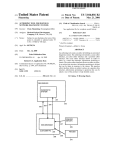
US005978902A
United States Patent [19]
[11] Patent Number:
Mann
[45]
[54]
[75]
DEBUG INTERFACE INCLUDING
OPERATING SYSTEM ACCESS OF A
SERIAL/ PARALLEL DEBUG PORT
Inventor:
Revill, Geoff, “Advanced On—chip Debug for ColdFire
Developers”, Embedded Systme Engineering, Apr./May
1997, pp. S2—S4.
Daniel P. Mann, Austin, Tex.
Larus, James R., Ef?cient Program Tracing, 8153 Computer,
No. 5, May 26, 1993, Los Alamitos, CA, pp. 52—61.
Advanced Micro Devices, “Am29040TMMicroprocessor
User’s Manual—29K Family”, Advanced Micro Devices,
Inc. 1994, pp. 12—1 through 12—26.
[21] Appl. No.1 08/992,276
Filed:
Nov. 2, 1999
OTHER PUBLICATIONS
[73] Assignee: Advanced Micro Devices, Inc.,
Sunnyvale, Calif.
[22]
Date of Patent:
5,978,902
(List continued on next page.)
Dec. 17, 1997
Primary Examiner—William M. Treat
Attorney, Agent, or Firm—Zagorin, O’Brien & Graham,
Related US. Application Data
LLP
[60]
Provisional application No. 60/043,070, Apr. 8, 1997.
[51]
Int. Cl.6 .................................................... .. G06F 11/00
[57]
[52]
US. Cl. ............................................. .. 712/227; 714/27
Adebug interface supports data transfer using read and Write
[58]
Field Of Search ............................. .. 712/227; 714/27,
system calls that communicate data Without stopping an
ABSTRACT
executing kernel. The printf( ) command passes an infor
mation string to an executing operating system. The infor
714/30, 38, 28; 395/50049
mation string summons the operating system to use a serial
[56]
References Cited
debug port to signal to a debug device, such as a host system,
that is connected to the serial port. The debug interface
U.S. PATENT DOCUMENTS
supported read and Write operations and system calls alloW
5,058,114
10/1991 Kuboki et al. .
5,321,828
6/1994 Phillips et a1. .
5,357,626
10/1994 Johnson et al. .
the kernel and executing applications softWare, respectively,
to continue executing during the read and Write data trans
fers. The debug interface includes support for a plurality of
extended function sideband signals that extend the function
ality of the read and Write functionality to alloW the pro
5,371,689 12/1994 Tatsuma.
5,491,793
5,533,192
2/1996 Somasundaram et al. .
7/1996 Hawley et al. ......................... .. 714/28
5,642,479
6/1997 Flynn.
While transferring data using read and Write operation. The
5,752,013
5,774,684
5/1998 Christensen et al. ................. .. 712/227
6/1998 Haines et a1. ......................... .. 710/129
extended function sideband signals include a command
5,774,708
5,848,264
cessor to concurrently run kernel and application programs
acknowledge signal (CMDACK), a dual-purpose break
6/1998 Klingler.
execution and trace control signal (BRTC), an execution
12/1998 Baird et a1. ...................... .. 395/500.49
5,867,644
2/1999 Ranson et a1.
5,889,988
3/1999
stopped and receive data signal (STOPTX), and an off-chip
trigger event signal (TRIG). The debug interface further
709/224
Held ...................................... .. 709/103
includes a buffer for transferred data The kernel may run a
?rst data transfer command Which is not fully transmitted
FOREIGN PATENT DOCUMENTS
When a second data transfer command is issued. The oper
316609
0530816A3
636976
762276
849670
5/1989
3/1993
2/1995
3/1997
6/1998
59-194245
11/1984
European
European
European
European
European
Pat.
Pat.
Pat.
Pat.
Pat.
Off.
Off.
Off.
Off.
Off.
ating system supports buffering of the data evoked by the
second data transfer command using a conventional queuing
operation.
16 Claims, 9 Drawing Sheets
Japan .
TRA E RECORD [20;0]
DATA m
STEERING
.
wan/M5110]
CPU-DATMOUTHI: 01]
'wWUDB-CMD
4
Jl/PeCMD-DONE
JMPeCMD-PENDYNG
RD-UDB-CVD
cwouPsEL/s: 01
cPuJNsHED 0110 l
ms
DARALLEL PORT
PROCESSOR
"WW5 m
STATE m
MACHINE
ICK
JTAG TAP
CON‘ROLLER
SERIAL m
DEBUG
sIAIE MACHINE
L
gamma L24
STAIE MACWE
TRACE 200
BUFFER
PORT
AND
L
TRACE PAD
INTERFACE-2L
PDATA PADR
mus. TRACE cw
5,978,902
Page 2
OTHER PUBLICATIONS
K5 HDT, e—mail describing K5 HDT, Jan. 11, 1997, pp. 1—6.
O’Farrell, Ray, “Choosing a Cross—Debugging Methodol
ogy”, Embedded Systems Programming, Aug. 1997, pp.
Motorola “CPU32 Reference Manual”, pp. 7—1 thru 7—13
84—89.
Ganssle, Jack G., “Vanishing Visibility, Part 2”, Embedded
Systems Programming, Aug. 1997, pp. 113—115.
Oj ennes, Dan, “Debugging With Real—Time Trace”, Embed
ded Systems Programming, Aug. 1997, pp. 50—52, 54, 56,
(admitted prior to Apr. 8, 1997).
Motorola “MEVB Quick Start Guide”, pp. 3—5 thru 7—2
(admitted prior to Apr. 8, 1997).
and 58.
IBM Techinical Disclosure Bulletin “Tailorable Embedded
Heinicke et al., “A Real Time Integrated Environment for
Motorola 680XX—based VME and FASTBUS Modules”,
Event Trace”, vol. 34, No. 7B, Dec. 1991, pp. 259—261.
Oct. 1989.
Intel “PentiumTMProcessor User’s Manual vol. 3: Architec
ture and Programming Manual”, 1994, pp. 17—1 through
17—9.
IEEE Transactions on Nuclear Science, vol. 36, iss. 5, pp.
1701—1705.
U.S. Patent
Nov. 2, 1999
g
Sheet 1 of9
ozm c SE28
wmsiom
8T L2
02% E2
§
50m%
58
N22:we
\
\
/
2052@058”:
E5
5,978,902
.UE
H
U.S. Patent
Nov. 2, 1999
Sheet 3 of9
5,978,902
5.35
mo€5m m6z<E5
A
cow
>:m65T<oN >m:65T<oN >.m65A<153 >5m61<5
5605
560
.25
m
U.S. Patent
Nov. 2, 1999
Sheet 4 of9
5,978,902
0H3E;g 829531 ; 1l56E520
mom
wow
/
20 3%2
E;2 51m0 :wE@252:
.UE
w
f§0M3E5;G
9Z952 ; 5a12:8
>
l25?913,2
wI;5ams, :wE@2575
_
I25?323
5c7m‘2l n0 9E8V1G2MIcQ
253%2 .5%52 289E5V19%\35:
U.S. Patent
Nov. 2, 1999
Sheet 7 of9
START DEBUG
5,978,902
LOAD/UNLOAD
NEW 38-BIT COMMAND,
CHECK FINISHED FLAG
702
WRITE DEBUG
INSTRUCTION TO
TAP CONTROLLER
704
LOAD/UNLOAD 38-BIT
SERIAL VALUE WITH
PENDING BIT SET
REPEAT LOAD/UNLOAD
OF 38—BIT COMMAND,
CHECK FINISHED FLAG
FIG. 7
START DEBUG
802
WRITE DEBUG
INSTRUCTION TO
TAP CONTROLLER
804
806
LOAD/UNLOAD
DEBUG SCAN CHAIN
WITH PENDING BIT SET
FIG. 8
U.S. Patent
Nov. 2, 1999
Sheet 8 of9
S
_ VB
O O O
_Emmi
_Emmi
@859;
g_ig
3T2I5E x9520 BQUJESL EUIJE T2'5l196
6259038
5,978,902
5,978,902
1
2
DEBUG INTERFACE INCLUDING
OPERATING SYSTEM ACCESS OF A
SERIAL/PARALLEL DEBUG PORT
information during a Branch Target Address (BTA) cycle.
The BTA-cycle is stolen from regular bus operation cycles.
HoWever in debug environments With high branch activity
and loW cache hit rates, BTA-cycles are often fully occupied
RELATED APPLICATIONS
handling branches, resulting in a con?ict over access to the
address bus that necessitates processor “throttle back” to
prevent a loss of instruction trace information. For example,
This application claims priority to US. application Ser.
No. 60/043,070, ?led Apr. 8, 1997, Which is hereby incor
softWare in the communications industry is branch-intensive
and suffers poor cache utiliZation often resulting in 20% or
porated by reference.
BACKGROUND OF THE INVENTION
10
In another approach, a second “trace” or “slave” processor
is combined With a main processor, With the tWo processors
microprocessors. More speci?cally, the present invention
operating in-step. Only the main processor fetches instruc
relates to a softWare debug support system and operating
method in processors.
15
increasing processor clock speeds, has placed an increasing
adequate softWare debug functionality in a processor results
in longer customer development times and reduces attrac
tiveness of the processor for use Within industry. SoftWare
debug support is particularly useful in the embedded prod
ucts industry, Where specialiZed on-chip circuitry is often
tions. The second, slave processor monitors fetched instruc
tions on the data bus and maintains an internal state in
2. Description of the Related Art
The groWth in softWare complexity, in combination With
burden on application softWare developers. The cost of
developing and debugging neW softWare products is noW a
signi?cant factor in processor selection. A failure to include
more throttle back, an unacceptable amount for embedded
products Which are subject to real-time constraints.
1. Field of the Invention
The present invention relates to computer systems such as
20
25
synchroniZation With the main processor. The address bus of
the slave processor supplies trace information. After poWer
up, via a JTAG (Joint Test Action Group) input, the second
processor is sWitched into a slave mode of operation. The
slave processor, freed from instruction fetch duties, uses the
slave processor address bus and other pins to supply trace
information.
Another existing debug strategy utiliZes implementation
of debug support into every processor in a system, but only
bonding-out signal pins in a limited number of packages.
combined With a processor core.
The bond-out versions of the processor are used during
The softWare debug tool con?guration of a processor
addresses the needs of several parties in addition to the
softWare engineer Who develops program code for execution
on the processor. A “trace” algorithm developer searches
through captured softWare trace data that re?ects instruction
debug and replaced With the smaller package for ?nal
production. The bond-out approach suffers from the need to
30
larly if a substantial number of extra pins are required by the
debug support variant. Furthermore, the debug capability of
execution How in a processor. An in-circuit emulator devel
oper deals With problems of signal synchroniZation, clock
frequency and trace bandWidth. A processor manufacturer
seeks a softWare debug tool solution that avoids an increased
processor cost or design and development complexity.
35
ging. HoWever, the initial task of getting the operating
systems running reliably often calls for special development
equipment While not standard in the desktop environment,
development equipment such as logic analyZers, read-only
memory (ROM) emulators, and in-circuit emulators (ICE)
specially-packaged processors is unavailable in typical
processor-based production systems.
In yet another approach, speci?cally the Background
Debug Mode (BDM) implemented by Motorola, Inc., lim
ited on-chip debug circuitry is implemented for basic run
In the desktop systems, complex multitasking operating
systems are currently available to support softWare debug
support additional bond pad sites in all fabricated devices, a
burden in small packages and pad limited designs, particu
40
control. The BDM approach utiliZes a dedicated serial link
having additional pins and alloWs a debugger to start and
stop the target system and apply basic code breakpoints by
inserting special instructions in system memory. Once
45
are sometimes used in the embedded industry. In-circuit
emulators have some advantages over other debug environ
halted, special commands are used to inspect memory vari
ables and register contents. The BDM system includes trace
support, but not conveniently using the serial link. Instead
ments including complete control and visibility over
the BDM system supplies trace support through additional
dedicated pins and expensive external trace capture hard
memory and register contents, and supplying overlay and
Ware that transfer instruction trace data.
trace memory if system memory is insuf?cient.
Traditional in-circuit emulators are used by interfacing a
ging suffer from a variety of limitations including increased
custom emulator back-end With a processor socket to alloW
packaging and development costs, circuit complexity, pro
communication betWeen emulation equipment and the target
system. The custom design of emulator interfaces in increas
ingly unrealistic and expensive as product life cycles are
reduced and nonstandard and exotic integrated circuit pack
ages are predominant in present day processor design.
FeW knoWn processor manufacturing techniques are
cessor throttling, and bandWidth matching difficulties.
Accordingly, present day techniques for softWare debug
Furthermore, no adequate loW-cost procedure for providing
55
available that include a suitable full-function in-circuit emu
lation functionality. Most processors in personal computer
In a conventional system, a processor discontinues execu
60
(PC) systems implement emulation functionality using a
multiplexed approach in Which existing pins are multiplexed
Some advanced processors multiplex debug pins in time,
for example by using the address bus to report softWare trace
tion in the debug mode and sets a stop transmit signal. An
external system detects assertion of a stop and interrogates
a debug port to determine the reason for termination of
for alternative use in a softWare debug application. Multi
plexing of pins is not desirable in embedded controllers,
Which inherently suffer from overload of pin functionality.
trace information is currently available. The limitations of
the existing solutions are likely to be exacerbated in the
future as internal processor clock frequencies continue to
increase.
65
execution. Reasons for termination include, for example, a
breakpoint, an illegal memory access, and transport of a
printf( ) data string. The conventional system accesses a
printf( ) data string, transfers the data string via the JTAG
port, sends the printf( ) data string to a source-debug
5,978,902
3
4
console, and sends a signal to the source-console designat
ing that the command is terminated, the processor has
stopped executing and the reason that execution is stopped.
The processor is then enabled to begin execution and the
interrupted program continues execution. Termination of
execution may be suitable for debugging in kernel mode, but
running of a softWare system and a debug interface con
nected to the processor core and connectable to an external
softWare debug device. The softWare system includes input/
output function calls. The external softWare debug device
detects operating signals generated by the processor core
during running of the softWare system. The softWare system
transfers debug information via the debug interface using the
is generally unacceptable in application mode for many
applications.
input/output function calls While the processor core contin
ues execution during a data transfer of the input/output
function calls.
The printf( ) data transfer is cumbersome because the
printf( ) command heavily intrudes into the operation of the
processor. In the conventional system, entry into debug
mode demands that the processor stops executing, and the
debug port generates a signal indicating that the processor
BRIEF DESCRIPTION OF THE DRAWINGS
The present invention may be better understood, and its
has stopped and the reason the processor has stopped is to
deliver a printf( ) string. Accordingly, in the conventional
15
system each time a printf( ) command is executed in the
kernel mode debug or an application mode by a target
system processor, the processor has to stop all ruing appli
cations and stop execution of the kernel.
AWell-knoWn and highly critical problem With in-circuit
draWings.
FIG. 1 is a schematic block diagram shoWing a softWare
debug environment utiliZing a softWare debug port accord
ing to an embodiment of the present invention.
FIG. 2 is a schematic block diagram illustrating details of
an exemplary embedded processor product incorporating a
emulation (ICE) systems is that a debug operation using ICE
demands that the process executing in the target processor
undergoing the debug operation must stop execution to
alloW examination of operating conditions and signals.
Therefore, the advantage of the ICE system in alloWing full
softWare debug port according to the present invention.
FIG. 3 is a simpli?ed block diagram depicting the rela
25
control and visibility of data such as program trace data is
countered by the disadvantage of stopping execution of the
processor. When the processor stops, all interrupt handling
stops, a highly disadvantageous condition in real-time envi
FIG. 4 is a ?oWchart illustrating softWare debug com
mand passing according to one embodiment of the inven
ronments such as communication and netWork environ
tion;
FIG. 5 is a ?oWchart illustrating enhanced softWare port
command passing according to a second embodiment of the
What is needed is an apparatus and operating technique
that alloWs a debug system full visibility and access to data,
including a program trace capability, While permitting the
invention; and
35
tinue running While the debug data is accessed.
SUMMARY OF THE INVENTION
debug interface supports data transfer using read and Write
system calls that communicate data Without stopping an
executing kernel. The printf( ) command passes an infor
mation string to an executing operating system. The infor
mation string summons the operating system to use a serial
45
supported read and Write operations and system calls alloW
FIG. 9 is a timing diagram shoWing signal behavior for
acquisition and release of a parallel debug bus.
FIG. 10 is a How chart depicting a parallel debug port
interface protocol folloWed by the host system during com
munications via the parallel port.
The use of the same reference symbols in different draW
ings indicates similar or identical items.
the kernel and executing applications softWare, respectively,
to continue executing during the read and Write data trans
fers. The debug interface includes support for a plurality of
extended function sideband signals that extend the function
ality of the read and Write functionality to alloW the pro
DESCRIPTION OF THE PREFERRED
EMBODIMENT(S)
cessor to concurrently run kernel and application programs
While transferring data using read and Write operation. The
extended function sideband signals include a command
FIGS. 6A—6G illustrate the general format of a variety of
trace buffer entries for reporting instruction execution
according to the invention.
FIG. 7 is a state diagram illustrating states of a standard
JTAG interface access operation.
FIG. 8 is a state diagram illustrating states of an enhanced
JTAG interface access operation.
In accordance With an aspect of the present invention, a
debug port to signal to a debug device, such as a host system,
that is connected to the serial port. The debug interface
tionship betWeen an exemplary instruction trace buffer and
other components of an embedded processor product
according to the present invention;
ments.
processor, kernel softWare and application softWare to con
numerous objects, features, and advantages made apparent
to those skilled in the art by referencing the accompanying
55
acknoWledge signal (CMDACK), a dual-purpose break
execution and trace control signal (BRTC), an execution
stopped and receive data signal (STOPTX), and an off-chip
trigger event signal (TRIG). The debug interface further
Referring to FIG. 1, a schematic block diagram illustrates
a softWare debug environment utiliZing a debug port 100. A
target system 101 is shoWn containing an embedded pro
cessor device 102 coupled to system memory 106. The
embedded processor device 102 is an integrated debug
interface for ?exible, high-performance in an embedded
hardWare/softWare debug system. The embedded processor
includes a buffer for transferred data. The kernel may run a
device 102 includes a processor core 104 and the debug port
100. In some embodiments, the embedded processor device
?rst data transfer command Which is not fully transmitted
When a second data transfer command is issued. The oper
102 may incorporate additional circuitry (not shoWn) for
ating system supports buffering of the data evoked by the
performing application speci?c functions, or may take the
second data transfer command using a conventional queuing
operation.
In accordance With an embodiment of the present
invention, a processor includes a processor core supporting
form of a stand-alone processor or digital signal processor.
65
In the illustrative embodiment, the debug port 100 includes
an IEEE-1149.1-1990 compliant JTAG interface or other
similar standardiZed serial port interface.
5,978,902
6
5
devices in response to internal breakpoints, and by elimi
nating status polling of the JTAG serial interface. The
sideband signals offer extra functionality and improve com
munications speeds for the debug port 100, but are optional
and not utiliZed in the simplest embodiments of debug port
100 Which uses conventional JTAG support signals. In the
illustrative embodiment the sideband signals are used With
an optional parallel port 214 provided on special bond-out
A host system 111 is used to execute debug control
software 112 for transferring high-level commands and
controlling the extraction and analysis of debug information
generated by the target system 101. The host system 111 and
target system 101 of the disclosed embodiment of the
invention communicate via a serial link 110. Most comput
ers are equipped With a serial or parallel interface Which can
be inexpensively connected to the debug port 100 by means
of a serial connector 108, alloWing most computers to
function as a host system 111. In some embodiments, the
serial connector 108 is replaced With higher speed JTAG
to-netWork conversion equipment.
Referring to FIG. 2, a schematic block diagram illustrates
the embedded processor device 102 in more detail, including
the processor core 104 and various elements of the debug
port 100 in an enhanced form. The embedded processor
device 102 includes a plurality of state machines that
10
15
data output signal TDO are received by the serial debug
shifter 212 via the JTAG TAP controller 204 so that com
communicate messages and data betWeen a serial port of a
J TAG TAP controller 204, a trace control circuit 218, and the
mands and data are loaded into debug registers 210 and read
from the debug registers 210. In the disclosed embodiment,
the debug registers 210 include tWo debug registers for
processor core 104. In some embodiments, the embedded
processor device 102 includes a parallel port 214 and the
state machines similarly establish communication betWeen
transmitting (TXiDATA register) and receiving (RXi
DATA register) data, an instruction trace con?guration reg
the parallel port 214, the trace control circuit 218, and the
ister (ITCR), and a debug control status register (DCSR).
processor core 104.
The state machines include a debug port state machine
206, a parallel port state machine 226, a processor interface
state machine 202, and a pending/?nished state machine
224. The state machines read the commands and data from
Data are typically read from the JTAG TAP controller 204
25
The Instruction Trace Con?guration Register (ITCR) is
Written to control enabling, disabling, and con?guration of
Instruction Trace debug functions. The ITCR is accessed
through the serial/parallel debug register Write/read com
mands or by using a reserved instruction LDTRC.
from memory, utiliZe processor core 104 intervention and
are appropriately sent to the processor core 104. The state
The Debug Control/Status Register (DCSR) indicates
35
When the processor core 104 enters debug mode and alloWs
the processor core 104 to be forced into debug mode using
the enhanced JTAG interface. DCSR also includes miscel
laneous control feature enables bits. DCSR is accessible
only through the serial/parallel debug register Write/read
commands.
A minimal embodiment of the debug port 100 supports
only conventional JTAG pins in a fast JTAG compliant
interface that advantageously attains controllability and
observability. The JTAG pins are a transportation mecha
nism that use existing pins to enter commands for perfor
mance by the processor core 104. Conventional JTAG pins
carry conventional JTAG support signals that are Well
knoWn in the art including a test clock signal TCK, a test
using a Capture DR-Update DR sequence in the JTAG TAP
controller state machine.
the serial/parallel ports and direct decoding of the com
mands by a command decode and processing block 208
logic. Some commands, such as a command for reading data
machines do not accept further commands until execution of
a previous command is complete. Once the command is
completed, a ?ag in a Debug Registers 210 block is asserted
or an output pin is asserted to indicate command completion
to the host system 111.
versions of the embedded processor device 102.
Using conventional JTAG signals, the JTAG TAP con
troller 204 accepts standard JTAG serial data and control
signals. When public JTAG DEBUG instruction is Written to
a JTAG instruction register, the serial debug shifter 212 is
connected to a serial interface formed by the JTAG TAP
controller 204. AJTAG test data input signal TDI and a test
A debug port state machine 206 coordinates loading and
reading of data betWeen the serial debug shifter 212 and the
debug registers 210. The debug port state machine 206
45
mode select signal TMS, a test data input signal TDI, and a
test data output signal TDO. The conventional JTAG pins
interfaces to the J TAG TAP controller 204 via a parallel port
state machine 226. Acommand decode and processing block
208, and the processor interface state machine 202, in
combination, decode commands and data and dispatch the
commands and data to a data steering circuit 222 Which, in
turn, communicates With the processor core 104 and trace
control circuit 218. The processor interface state machine
202 communicates directly With the processor core 104 and
a trace control circuit 218. Aparallel port 214 communicates
are driven by a JTAG Test Access Port (TAP) controller 204.
The JTAG interface is enhanced to improve softWare
debug capabilities and to transfer high-level commands into
With the debug port state machine 206 and the data steering
circuit 222 to perform parallel data read and Write operations
in optional bond-out versions of the embedded processor
the processor core 104, rather than to scan processor pins.
The JTAG-compliant serial interface is augmented for
higher-speed access via supplemental sideband signals and
bondout package to fully support the enhanced 10-pin debug
device 102.
The trace control circuit 218 generates trace record infor
mation for reconstructing instruction execution How in the
processor core 104. The trace control circuitry 218 interfaces
port 100 format. The enhanced embodiment of the debug
port 100 supports the four additional pins carrying “side
trace pad interface port 220, Which is also called a DEBUG
band” signals including a command acknowledge signal
trace port 220, or to an internal trace buffer 200 and
CMDACK, a break request/trace capture signal BRTC, a
stop transmit signal STOPTX, and a trigger signal TRIG to
the standard JTAG interface. The additional sideband signals
implements user control for selectively activating and deac
tivating trace functionality. The trace control circuitry 218
a bond-out parallel interface With a 16-bit data path.
Speci?cally, four pins are added to an embedded processor
device 102 that supports JTAG functionality in a non
advantageously enhance performance and functionality of
the debug port 100 by attaining highly precise external
breakpoint assertion and monitoring, by triggering external
55
to the processor core 104 and supports tracing either to a
65
controls a trace pad interface port 220 Which, in the illus
trative embodiment, shares communication lines of the
parallel port 214. When utiliZed, the trace pad interface port
220 supplies trace data While the processor 104 is executing
5,978,902
7
8
instructions, although clock synchronization and other dif
to the parallel port 214 until the trace buffer 220 is empty.
?culties may arise. The trace control circuitry 218 enables
The trace buffer 220 is functionally used as a circular buffer
other features including programmability of synchronization
for the internal trace mode of operation. Trace records
overWrite existing data after 256 records are Written into the
trace buffer 200.
address generation and user speci?ed trace records.
The processor core 104 supplies the tracing information
that is used to generate trace records. The debug port
interface 100 supplies the commands to enable and disable
The JTAG TAP controller 204 functions as an IEEE
1149.1-1990-compliant serial command port that serves as a
the trace function, and to turn trace capture on and off via the
ITCR. Commands to read the trace buffer come from the
processor core 104. At reset, tracing is disabled and trace
10
debug port 100 using only conventional JTAG signals, the
port 100 is enabled by Writing the public JTAG instruction
capture is turned off. To begin generating trace records,
tracing is enabled and trace capture turned on. When the
processor core 104 enters the debug mode, trace capture is
turned off. When the processor core 104 exits debug mode,
trace capture status returns to the state prior to entering
primary mode of communication betWeen a host processor
111 and target processor to a maximum TCK rate of 25
MHZ. Before debug information is communicated via the
15
debug mode.
DEBUG into a JTAG instruction register contained Within
the J TAG TAP controller 204. The J TAG instruction register
is a 38-bit register including a 32-bit data ?eld debugidata
[31:0], a four-bit command ?eld cmd[3:0] to point to various
internal registers and functions provided by the debug port
Tracing is enabled by setting the GTEN bit in the ITCR.
Tracing is disabled by resetting the GTEN bit. When tracing
is disabled, all trace records are discarded from the trace
100, a command pending ?ag (P), and a command ?nished
?ag
Some commands use bits of the debugidata ?eld
buffer 200. Trace capture is turned on by setting the TRON
bit in the ITCR. Trace capture is turned off by resetting the
The pending and ?nished ?ags are controlled by a pending/
TRON bit. The TRON bit is modi?ed in one of several Ways
?nished state machine 224 that is connected to the JTAG
TAP controller 204.
as a sub-?eld to extend the number of available commands.
including directly Writing to the TRON register, applying the
break request/trace capture signal BRTC if the BTRC is
enabled in the DCSR to control trace capture, and via
25
J TAG Instruction Register
DRO—DR3 register usage to turn trace capture on/off by
enabling the option in the ITCR.
The disabling of trace gathering is advantageously a
softWare option, reducing processor poWer consumption and
eliminating natural throttle-back tendencies. Trace gathering
37
is enabled both from the host system 111 and the target
system 101. Trace information is not generated When the
test mode select signal TMS. The test mode select signal
TMS alloWs the JTAG clocking path to be changed in the
2
This JTAG instruction register is selected by toggling the
processor is operating in Debug mode. All other modes may
be “traced” if the appropriate sWitches are set.
When tracing is disabled, contents of the trace buffer 200
are lost. HoWever, When commands or trace/breakpoint
54
debugfdata[31:0]
scan path, enabling usage of multiple paths of varying
35
control registers are used to temporarily stop/start trace
accumulation, the trace buffer 200 is not ?ushed.
lengths. Preferably, the JTAG instruction register is acces
sible via a short path. This register is con?gured to include
a soft register for holding values to be loading or receiving
from speci?ed system registers.
Referring noW to FIG. 3, a simpli?ed block diagram
depicts the relationship betWeen an exemplary instruction
The trace control circuit 218 operates in one of tWo
modes, external trace mode and internal trace mode, that
trace buffer 200 and other components of an embedded
differ in hoW the controller handles the trace records asso
processor device 102. In one embodiment, the trace buffer
ciated With trace events. The external trace mode is available
200 is a 25 6 entry ?rst-in, ?rst-out (FIFO) circular cache that
on a bondout chip. In external trace mode, trace records are
records the most recent trace entries. Increasing the siZe of
sent to the trace port 220. External trace mode is enabled by 45 the trace buffer 200 increases the amount of instruction trace
setting ITM=1 in the ITCR. The internal trace buffer tem
information that is captured, although the amount of
porarily stores trace records that cannot be sent to the trace
required silicon area may increase.
port at the same rate as the records are generated by the
The trace buffer 200 stores a plurality of 20-bit (or more)
processor core 104.
trace entries indicative of the order in Which instructions are
The internal trace mode is available on both a bondout and
executed by the processor core 104. Other information, such
a non-bondout integrated circuit. In the internal trace mode,
as task identi?ers and trace capture stop/start information, is
also placed in the trace buffer 200. The contents of the trace
buffer 200 are supplied to external hardWare, such as the
trace records are stored in the internal trace buffer 200. The
internal trace mode is enabled by setting ITM=0 in the
ITCR. The trace buffer 200 contents are accessed either
The trace buffer 200 improves bandWidth matching and
reduces the need to incorporate throttle-back circuitry in the
host system 111, via either serial or parallel trace pins 230.
Alternatively, the target system 101 can be con?gured to
examine the contents of the trace buffer 200 internally.
Referring to FIG. 4, a high-level ?oW chart illustrates a
technique for passing a command When using a standard
processor core 104. In one embodiment, the trace buffer 200
JTAG interface. Upon entering debug mode in step 400 the
is a 256 entry ?rst-in, ?rst-out (FIFO) circular cache.
Increasing the siZe of the trace buffer 200 increases the
amount of softWare trace information that is captured.
DEBUG instruction is Written to the TAP controller 204 in
step 402. In step 404, the 38-bit serial value is shifted in as
through debug port commands or through the enhanced x86
instruction STBUF.
55
a Whole, With the command pending ?ag set and desired data
When the processor core 104 takes a debug trap, the trace
(if applicable, otherWise Zero) in the data ?eld. Control
buffer might contain trace records. The processor core 104
proceeds to step 406 Where the pending command is loaded/
Will continue to send trace records to the trace port 220 until 65 unloaded and the command ?nished ?ag checked. Comple
the buffer is empty. If the TBUS signals are shared With the
tion of a command typically involves transferring a value
betWeen a data register and a processor register or memory/
parallel debug port 214, the trace port 220 does not switch
5,978,902
10
IO location. After the command has been completed, the
processor 104 clears the command pending ?ag and sets the
command ?nished ?ag, at the same time storing a value in
the data ?eld if applicable. The entire 38-bit register is
scanned to monitor the command ?nished and command
pending ?ags. If the pending ?ag is reset to Zero and the
?nished ?ag is set to one, the previous command has
command ?nished ?ag status is accessible When using the
?nished. The status of the ?ags is captured by the debug port
not started by the host system 111 until the command
state machine 206. A slave copy of the ?ag status is saved
internally to determine if the next instruction should be
loaded. The slave copy is maintained due to the possibility
of a change in ?ag status betWeen TAP controller 204 states,
alloWing the processor 104 to determine if the previous
instruction has ?nished before loading the next instruction.
If the ?nished ?ag is not set as determined in step 408,
control proceeds to step 410 and the loading/unloading of
the 38-bit command is repeated. The command ?nished ?ag
is also checked. Control then returns to step 408. If the
?nished ?ag is set as determined in step 408, control returns
to step 406 for processing of the next command. DEBUG
mode is exited via a typical JTAG process.
Returning to FIG. 2, the optional sideband signals are
utiliZed in the enhanced debug port 100 to provide extra
command acknoWledge signal CMDACK Without shifting
out the JTAG instruction register. The command acknoWl
edge signal CMDACK transitions high on the next rising
edge of the test clock signal TCK after the command
?nished ?ag has changed from Zero to one. When using the
enhanced JTAG signals, a neW shift sequence in step 506 is
10
With the test clock signal TCK. The test clock signal TCK is
not necessarily clocked at all times, but is ideally clocked
continuously When Waiting for a command acknoWledge
signal CMDACK response.
15
OPERATING SYSTEM/APPLICATION
COMMUNICATION VIA THE DEBUG PORT
Also included in debug register block 210 is an instruction
trace con?guration register (ITCR), a 32-bit register for
enabling/disabling and con?guring instruction trace debug
functions. Numerous functions are contemplated including
various levels of tracing, trace synchroniZation force counts,
trace initialiZation, instruction tracing modes, clock divider
functionality. The optional sideband signals include a break
request/trace capture signal BRTC that functions as a break
request signal or a trace capture enable signal depending on
the status of bit set in the debug control/status register. If set
to function as a break request signal, the break request/trace
capture signal BRTC is asserted to cause the processor 104
acknoWledge signal CMDACK pin is asserted high. The
command acknoWledge signal CMDACK is synchronous
25
ratio information, as Well as additional functions shoWn in
the folloWing table. The ITCR is accessed through a JTAG
instruction register Write/read command as is the case With
the other registers of the debug register block 210, or via a
reserved instruction.
to enter debug mode. The processor 100 is also stopped by
Instruction Trace Con?guration Register ITCR
scanning in a halt command via the convention JTAG
signals. If set to function as a trace capture enable signal,
BIT
asserting the break request/trace capture signal BRTC
enables trace capture. Deasserting the signal turns trace
capture off. The signal takes effect on the next instruction
boundary after the signal is detected and is synchroniZed
SYMBOL
31 :30 Reserved
35 29
RXINTEN
28
TXINTEN
DESCRIPTION/FUNCTION
Reserved
Enables interrupt When RX bit is set
Enables interrupt When TX bit is set
27
TX
The trigger signal TRIG is con?gured to pulse Whenever
26
RX
an internal processor breakpoint has been asserted. The
trigger signal TRIG may be used to trigger an external
25
24
DISL1TR
DISLOTR
Disables level 1 tracing
Disables level 0 tracing
23
DISCSB
Disables current segment base trace record
With the internal processor clock. The break request/trace
capture signal BRTC is selectively asserted at any time.
capturing device such as a logic analyZer, and is synchro
niZed With the trace record capture clock signal TRACE
CLK. When a breakpoint is generated, the event is synchro
niZed With the trace capture clock signal TRACECLK, after
Which the trigger signal TRIG is held active for the duration
and placed in the RXiDATA register
22:16 TSYNC[6:O] Sets the maximum number of Branch Sequence
trace records that may be output by the trace control
block before a synchronizing address record is
forced
45
of trace capture.
The stop transmit signal STOPTX is asserted When the
processor 104 has entered DEBUG mode and is ready for
register interrogation/modi?cation, memory or I/O reads and
Writes through the debug port 100. In the disclosed embodi
ment of the invention, the stop transmit signal STOPTX
re?ects the state of a bit in the debug control status register
(DCSR). The stop transmit signal STOPTX is synchronous
55
With the trace capture clock signal TRACECLK.
15
14
13
12
TSR3
TSR2
TSR1
TSRO
Sets
Sets
Sets
Sets
described in conjunction With FIG. 5, Which shoWs a sim
11
1O
9
8
TRACE3
TRACE2
TRACE1
TRACEO
Enables
Enables
Enables
Enables
7
6:4
TRON
TCLK[2:O]
3
ITM
Trace on/off
Encoded divider ratio between internal processor
clock and TRACECLK
Sets internal or external (bond-out) instruction trac
2
TINIT
Trace initialization
1
TRIGEN
Enables pulsing of external trigger signal TRIG
clears
clears
clears
clears
Trace
Trace
Trace
Trace
trace
trace
trace
trace
mode
mode
mode
mode
mode
mode
mode
mode
on
on
on
on
toggling
toggling
toggling
toggling
DR3
DR2
DR1
DRO
trap
trap
trap
trap
using
using
using
using
DR3
DR2
DR1
DRO
following receipt of any legacy debug breakpoint;
pli?ed command passing operation in the enhanced debug
independent of the Debug Trap Enable function in
port 100 of FIG. 2. A DEBUG instruction is Written to the
the DCSR
O
TAP controller 204 in step 502 to place the target system 111
into DEBUG mode. Control proceeds to step 504 and the
GTEN
Global enable for instruction tracing through the
internal trace buffer or via the external (bond-out)
interface
command acknoWledge signal CMDACK is monitored by
system 111 simultaneously With the command ?nished ?ag
and remains high until the next shift cycle begins. The
or
or
or
or
ing mode
The command acknoWledge signal CMDACK is
the host system 111 to determine command completion
status. The CMDACK signal is asserted high by the target
Indicates that the target system 111 is ready to
transmit data to the host system 111 and the data is
available in the T'XiDATA register
Indicates that data has been received from the host
65
Another debug register is the debug control/status register
(DCSR) that designates When the processor 104 has entered
debug mode and alloWs the processor 104 to be forced into
5,978,902
11
12
These read-Write services are supported by operating
DEBUG mode through the enhanced JTAG interface. As
shown in the following table, the DCSR also enables mis
system or device driver softWare that can control the opera
cellaneous control features including forcing a ready signal
tions and communication of data by other debug ports.
These services typically include read and Write services and
to the processor 104, controlling memory access space for
accesses initiated through the debug port, disabling cache 5 control selection services. Library layer operations such as
?ush on entry to the DEBUG mode, supplying transmit and
printf( ) and scanf( ) system calls include formatting soft
received bits TX and RX, enabling the parallel port 214,
forced breaks, forcing a global reset, and other functions.
Ware and utiliZe loW-level services. The printf() and scanf()
system calls, When operating at the application privilege
The ordering or inclusion of the various bits in either the
ITCR or DCSR is a design choice that typically depends on
level make privilege system calls to access loW-level ser
vices.
the application and processor implementing the debug sys
In a multitasking operating system, the illustrative embed
ded processor device 102 supports a debug functionality
during the operating of a plurality of tasks permitting
tem.
Debug ControlZStatus Register DCSR
15
BIT
SYMBOL
31:12 Reserved
11
TX
DESCRIPTION/FUNCTION
environments. Similarly, the embedded processor device
Reserved
While executing various types of programs that control
102 supports testing and analysis of the target system 101
Indicates that the target system 111 is ready to
transmit data to the host system 111 and the data is
available in the TXiDATA register
Indicates that data has been received from the host
20
and placed in the RXiDATA register
9
8
DISFLUSH
SMMSP
Disables cache ?ush on entry to DEBUG mode
STOP
cesses initiated through the Debug Port 100
Indicates Whether the processor 104 is in
DEBUG mode (equivalent to stop transmit
5
FRCRDY
BRKMODE
25
DBTEN
parallel port 214. Debug softWare may be generated that
Enables entry to debug mode or toggle trace mode
35
mechanisms
2
PARENB
DSPC
1
FBRK
O
FRESET
generates printf( ) statements in operating tasks including
debug printf( ) statements, but also include nondebug
printf( ) statements including operating system and applica
tion printf( ) statements. The combined debug, operating
system, and application information may be formatted on a
Enables parallel port 214
display screen in various con?gurations to produce highly
Disables stopping of internal processor clocks in the
Halt and Stop Grant states
informative displays. The embedded processor device 102
supports communication of character strings throughout the
Forces processor 104 into DEBUG mode at the next
instruction boundary (equivalent to pulsing the
external BRTC pin)
function calls, respectively, that advantageously extend the
debug functionality of the target system 101. For example,
be used to control debug hardWare and softWare including
the debug port such as the serial debug port (SDP) and the
enable on a trap/fault via processor 104 registers
DRO-DR7 or other legacy debug trap/fault
input and output interactions via the scanf( ) and printf( )
an I/O control function call and other loW level services may
Forces the ready signal RDY to the processor 104
to be pulsed for one processor clock; useful When it
is apparent that the processor 104 is stalled Waiting
for a ready signal from a non-responding device
Selects the function of the break request/trace cap
ture signal BRTC (break request or trace capture
on/off)
4
the problems of conventional debug systems in integrating
operating system softWare, in-circuit emulation hardWare,
The illustrative embedded processor device 102 supports
signal STOPTX
6
multiple hardWare subsystems.
Operating system support of debug functionality avoids
and target system hardWare.
Controls memory access space (normal memory
space/system management mode memory) for ac
7
in-depth testing and analysis of the operations of the target
system 101 in multiple various operating conditions and
40
target system 101, for example through printf( ) support of
the JTAG TAP controller 204, the parallel port 214, and the
Forces global reset
trace port 220. The embedded processor device 102 further
supports communication of the data from the target system
101 to the host system 111 using kernel mode and applica
When operating in a cross debug environment such as the
environment shoWn in FIG. 1, a parent task running on the 45 tion debug softWare support to display information on a
target system 111 sends information to the host platform 101
that controls the target system 101. The information may
include, for example, a character stream from a printf() call
or register information from a Task Control Block (TCB). In
one technique for transferring the information, an operating
system places the information in a knoWn region then causes
source debugger console WindoW. Debug information is
transferred using the kernel printf( ) command With the
processor core 104 continuing execution during the printf()
data transfer.
In one embodiment of a target system 101 that includes
debug functionality, softWare supports an application mode
printf( ) command and a kernel mode printf( ) command.
DEBUG mode to be entered via a trap instruction.
The printf( ) call is a Well-knoWn function or procedure
call in programming languages such as tie C++ language and
The embedded processor device 102 is speci?ed to operate
so that the processor core 104 continues to execute during
is typically supported in operating systems including various
execution of a printf( ) command and during transfer of a
WindoWsTM operating systems such as WindoWs CETM. In
in the processor core 104 of the target system 101 supports
printf( ) data string. The debug port 100 responds to acti
vating signals from the host system 111 by generating
a printf( ) call that generates signals to the processor
interface state machine 202 to support operating system
printf( ) command and quickly enter the kernel operating
the illustrative embodiment, an operating system performing
access to information stored in the trace buffer 200.
The read-Write services and function calls advantageously
make debug information available to the operating system
Which may be exploited by the operating system to enable
the operating system to perform debug functions.
Accordingly, the operating system attains a debug function
ality Without adding the signi?cant hardWare of conven
tional debug tools.
signals that cause the processor core 104 to perform a
60
mode and assemble a character string that causes the pro
cessor core 104 to enter the debug mode.
The embedded processor device 102 supports data trans
fer using printf() and scanf( ) commands that communicate
data Without stopping an executing kernel. The printf( )
command passes an information string to an executing
operating system. The information string summons the oper
ating system to use a serial debug port 100 to signal to a
5,978,902
14
13
The information transfer technique using the RXiDATA
debug device, such as the host system 111, that is connected
to the serial port 100. The embedded processor device
supported printf( ) command allows the kernel and execut
ing applications softWare to continue executing during the
printf( ) data transfer. The embedded processor device 102
and TXiDATA registers enables an operating system or
application to communicate With the host system 111 With
out stopping processor 104 execution. Communication is
conveniently achieved via the debug port 100 With minimal
includes support for a plurality of extended function side
impact to on-chip application resources. In some cases it is
band signals that extend the functionality of the printf( )
necessary to disable system interrupts. This requires that the
command to alloW the processor to concurrently run kernel
RX and TX bits be examined by the processor 100. In this
situation, the communication link is driven in a polled mode.
and application programs While transferring data using a
printf( ) command. The extended function sideband signals
10
include a command acknowledge signal (CMDACK), a
dual-purpose break execution and trace control signal
(BRTC), an execution stopped and receive data signal
(STOPTX), and an off-chip trigger event signal (TRIG).
PARALLEL INTERFACE TO DEBUG PORT 100
The serial debug port (SDP) is accessed either With the
15
JTAG-based serial link (JTAG based) or a someWhat more
The kernel may run a ?rst printf( ) command Which is not
parallel interface. The parallel port 214 interface supports
fully transmitted When a second printf( ) command is issued.
The operating system supports buffering of the data evoked
by the second printf( ) command using a conventional
higher code doWn-load speeds, but is included in a bond-out
part. Full-function ICE developers are typical users of the
bond-out parts.
queuing operation.
A full-function In Circuit Emulator (ICE) uses a dual
The host system 111 uses debug port 100 commands to
determine the reason for entering DEBUG mode and
ported pod-space memory to gain high speed access to the
target system 101 to gain faster doWn-load speeds than are
responds by retrieving the information from the reserved
region. HoWever, normal processor execution is stopped
relatively complex dual-port design that is different for
While the processor 104 is in DEBUG mode, an undesirable
available With the serial debug port alone. To avoid a
25
The undesirable condition is addressed in the illustrative
various target processors, an alternative the T/P input pin is
implemented in bond-out versions only and used to sWitch
the bond-out pins from a trace mode to parallel port mode.
system by supplying tWo debug registers in the debug port
100 including registers for transmitting data (TXiDATA
register) and receiving (RXiDATA register) data. The
Some embedded systems specify that instruction trace is
to be examined While maintaining I/O and data processing
operations. Without the use of a multi-tasking operating
condition for real-time systems.
TXiDATA and RXiDATA registers are accessed using the
soft address and JTAG instruction register commands. The
soft address is auto-incremented to assist data transfer. After
the host system 111 Writes a debug instruction to the JTAG
system, a bond-out version of the embedded processor
35
instruction register, the serial debug shifter 212 is connected
to the test data input signal TDI line and test data output
signal TDO line.
In the disclosed embodiment, a parallel port 214 is
implemented in an optional bond-out version of the embed
ded processor device 102 to support parallel command and
data access to the debug port 100. The parallel port 214
interface forms a 16-bit data path that is multiplexed With the
The processor 104 executes code that transmits data by
?rst testing a TX bit in the ITCR. If the TX bit is set to Zero
then the processor 104 executes either a memory or I/ O Write
instruction to transfer the data to the TXiDATA register.
The debug port 100 sets the TX bit in the DCSR and ITCR,
indicating to the host system 111 a readiness to transmit data,
and asserts the STOPTX pin high. After the host system 111
trace pad interface port 220. More speci?cally, the parallel
port 214 supplies a 16-bit Wide bi-directional data bus
45
TRACECLOCK (TC). Although not shared With the trace
register, the TX bit is set to Zero. A TXINTEN bit in the
ITCR is then set to generate a signal to interrupt the
pad interface port 220, a parallel bus request/grant signal
pair PBREQ/PBGNT (not shoWn) are also implemented.
processor 104. The interrupt is generated only When the TX
The parallel port 214 is enabled by setting a bit in the DCSR.
bit in the ITCR transitions to Zero. When the TXINTEN bit
Serial communications via the debug port 100 are not
is not set, the processor 104 polls the ITCR to determine the
status of the TX bit to further transmit data.
disabled When the parallel port 214 is enabled.
The host system 111 transmits data by ?rst testing a RX
55
The bond-out TC pin is a trace capture clock, a clock
signal that is also used to capture system memory accesses
performed on other busses. Capturing system bus activity is
used to trace bus activity in conjunction With program trace.
The TC clock is preferentially accessed last in a sequence of
clock signals since system bus data can be acquired at the
time of the TC clock signal. Thus other bus signals are to
remain active at the time of the TC clock, or be latched in
the ICE preprocessor and held until the TC clock is active.
processor 104. This interrupt is only generated When the RX
in the ITCR transitions to one. When the RXINTEN bit is
not set, the processor 104 polls the ITCR to verify the status
of the RX bit. If the RX bit is set to one, the processor
instruction is executed to read data from the RXiDATA
When the parallel port 214 is selected, rather than the
register. After the data is read by the processor 104 from the
RXiDATA register the RX bit is set to Zero. The host
(PDATA[15 10]), a 3-bit address bus (PADR[2:0]), a parallel
debug port read/Write select signal (PRW), a trace valid
signal TV and an instruction trace record output clock
completes reading the transmit data from the TXiDATA
bit in the ITCR. If the RX bit is set to Zero, the host system
111 Writes the data to the RXiDATA register and the RX bit
is set to one in both the DCSR and ITCR. A RXINT bit is
then set in the ITCR to generate a signal to interrupt the
device 102 is preferable to supply trace data since,
otherWise, examination of the trace buffer 200 via the debug
port 100 requires the processor 104 to be stopped.
65
trace port 220, the TC clock is used to read and Write
parameters in to the Debug Registers 210, a faster process
system 111 continuously reads the ITCR to determine the
than serially clocking data into the 38-bit JTAG instruction
status of the RX bit to further send data.
command register.
5,978,902
15
16
offers full visibility of execution history without throttling
the processor core 104. The trace buffer 200, if needed, is
con?gured for use as a buffer to the parallel port 214 to
Bond-Out Pins/Parallel Port 214 Format
21
TV
2O
TC
19
PRW
alleviate bandwidth matching issues.
16
PADR [2:0]
OPERATING SYSTEM AND DEBUGGER
INTEGRATION
PDATA [15:0]
The parallel port 214 is primarily intended for fast
downloads/uploads to and from target system 111 memory.
However, the parallel port 214 may be used for all debug
communications with the target system 111 whenever the
processor 104 is stopped. The serial debug signals, either
In the illustrative embodiment, the operation of all debug
10
from a monitor program, a target hosted debugger, or
conventional pod-wear. The debug port 100 performs data
standard or enhanced, are used for debug access to the target
system 111 when the processor 104 is executing instructions.
In a manner consistent with the JTAG standard, all input
15
is very similar to operations in DEBUG mode from a
monitor program. All debug operations are controlled via
processor instructions, whether the instructions are accessed
the disclosed embodiment, the parallel port 214 shares pins
from pod-space or regular memory, advantageously extend
ing an operating system to include additional debug capa
with the trace pad interface 220 so that commands directed
to the parallel port 214 are initiated only while the processor
bilities.
104 is stopped and the trace pad interface 220 is discon
nected from the shared bus.
Operating systems have supported debuggers via privi
25
grant signal PBGNT are included to expedite multiplexing
of the shared bus signals between the trace buffer 200 and
the parallel port 214. When the host interface to the parallel
port 214 detects that the parallel bus request signal PBREQ
leged system calls such a ptrace( ) call for some time.
However, the incorporation of an on-chip trace buffer 200
now enables an operating system to offer instruction trace
capability. The ability to trace is often considered essential
in real-time applications. In the illustrative improved debug
environment, functionality of an operating system is
is asserted, the host interface begins driving the parallel port
214 signals and asserts the parallel bus grant signal PBGNT.
enhanced to support limited trace without the incorporation
of an external logic analyZer or in-circuit emulator.
When entering or leaving DEBUG mode with the parallel
port 214 enabled, the parallel port 214 is used for the
Instructions that support internal loading and retrieving of
processor state save and restore cycles. The parallel bus
request signal PBREQ is asserted immediately before the
moves that are initiated by serial data port commands rather
than processor instructions.
Operation of the processor from conventional pod-space
signals to the parallel port 214 are sampled on the rising
edge of the test clock signal TCK and all output signals are
changed on the falling edge of the test clock signal TCW In
The parallel bus request signal PBREQ and parallel bus
supporting features including the trace buffer 200 is con
trolled through the debug port 100 or via processor instruc
tions. The processor instructions are commonly accessed
35
beginning of a save state sequence penultimate to entry of
DEBUG mode. On the last restore state cycle, the parallel
bus request signal PBREQ is deasserted after latching the
write data. The parallel port 214 host interface responds to
parallel bus request signal PBREQ deassertion by tri-stating
its parallel port drivers and deasserting the parallel bus grant
signal PBGNT. The parallel port 214 then enables the debug
trace port pin drivers, completes the last restore state cycle,
asserts the command acknowledge signal CMDACK, and
trace buffer 200 contents include a load instruction trace
buffer record command LITCR and a store instruction trace
buffer record command SITCR. The command LITCR loads
an indexed record in the trace buffer 200 speci?ed by a trace
buffer pointer ITREC.PTR with the contents of the EAX
register of the processor core 104. The trace buffer pointer
ITREC.PTR is pre-incremented, so that the general opera
tion of the command LITCR is described, as follows:
ITREC.PTRGITRCECPTRH;
ITRREC[ITREC.PTR]+EAX.
If the instruction trace record, in a trace record format
returns control of the interface to trace control circuit 218. 45 described hereinafter, is smaller that the EAX record, only a
portion of the EAX register is used.
During communication via the parallel port 214, the
Similarly, the store instruction trace buffer record com
mand SITCR is used to retrieve and store into the EAX
register an indexed record from the trace buffer 200. The
contents of the ECX register of the processor core 104 are
used as an offset that is added to the trace buffer pointer
ITREC.PTR to create an index into the trace buffer 200. The
address pins PADR[2:0] are used for selection of the ?eld of
the JTAG instruction register, which is mapped to the 16-bit
data bus PDATA[15 :0] as shown in the following table:
PADR[2:O]
Data Selection
000
No selection (null operation)
001
4-bit command register; command driven on PDATA[3:O]
010
High 16-bits of debugidata
011
Low 16-bits of debugidata
100-111
Reserved
ECX register is post-incremented while the trace buffer
pointer ITREC.PTR is unaffected, so that:
55
EAXeITREC[ECX+ITREC.PTR];
ECXGECXH.
The LITCR and SITCR commands may be con?gured in
numerous variations of formats that are known in the
computing and encoding arts.
Extension of the operating system to support on-chip trace
has many advantages. In the communications industry, sup
port of on-chip trace maintains system I/O and communi
If only a portion of the bits of the debug data [31:0]
register are utiliZed during a transfer, such as on 8-bit I/O
cycle data write operations, only the used bits need be
updated. The command pending ?ag is automatically set
when performing a write operation to the four-bit command
register and is cleared when the command ?nished ?ag is
asserted. The host system 111 monitors the command
acknowledge signal CMDACK to determine when the ?n
ished ?ag has been asserted. Use of the parallel port 214
cation activity while a task is traced. Traditionally, the use of
most in-circuit emulators has demanded that the processor
65
be stopped and operating system execution suspended
before the processor state and trace are examined, disrupting
continuous support of I/O data processing. In contrast, the
5,978,902
17
18
ptrace( ) capabilities of the illustrative enhanced system
address and attributes, the vector number of the exception
handler, and the EIP of the target instruction in the interrupt
handler.
A hardWare interrupt generates trace records that report
alloW the processor and operating system to continue execu
tion While trace data is available.
The trace buffer 200 is highly useful in applications
controlling ?eld equipment. If an unexpected system crash
the EIP of the instruction that Was most recently executed
before the interrupt Was serviced, the previous segment base
address and attributes, the vector number of the interrupt
handler, and the EIP of the target instruction in the interrupt
occurs, the trace buffer 200 can be examined to observe the
execution history leading up to the crash event. When used
in portable systems or other environments in Which poWer
handler.
consumption is a concern, the trace buffer 200 can be
disabled via poWer management circuitry. A trace record is
10
read from the trace buffer 200 that includes a record of trace
A trace synchroniZation register implemented in the trace
controller is used to generate a trace synchroniZation event.
events. Atrace event is an action that causes trace records to
The trace synchroniZation register is updated from the
be generated. Trace events are caused, for example, by x86
instructions, instructions causing an exception, hardWare
interrupts, trace synchroniZation events, activation or deac
tivation of trace capture, and events that change privilege
TSYNC bits of the ITCR register Whenever the ITCR is
loaded. The trace synchroniZation register is decremented by
15
level.
Several x86 instructions generate trace records including
1 When a conditional branch trace record (TCODE=OOO1) is
created. Any other trace record causes the register to be
reloaded from the TSYNC bits of the ITCR register. The
register counts doWn to Zero and generates a trace event. The
IRETD) instructions, jump (JMP) and conditional jump
trace synchroniZation is then reloaded from the TSYNC bits
of the ITCR register. The TSYNC value represents the
maximum number of consecutive conditional branch trace
records (TCODE=OOO1) created before a trace synchroni
(JCC) instructions, LOOP instructions, MOV CRO
Zation event occurs. A TSYNC value of O disables trace
softWare interrupt instructions, BOUND instructions, CALL
instructions, interrupt taken and not taken (INT/INTO)
instructions, return (RET) and interrupt return (IRET/
synchroniZation events.
instructions, and the like. A REP pre?x does not generate a
trace record.
25
All CALL and CALLS instructions in Which the target
address is supplied by a register or memory location produce
a TCODE=OO1O entry. If the target address arises from the
Which trace capture Was turned on.
Trace records are generated When trace capture is turned
off. The trace records report the EIP of the instruction at
Which trace capture Was turned off and optionally the base
address and segment attributes of the current segment.
Generation of trace records With the current segment base is
instruction (an immediate address) no TCODE=OO1O entry
is used. If a segment change occurs (a long address) then a
TCODE=OO11 entry is generated ahead of a TCODE=OO1O
entry. A segment change entry may be generated even if no
target address entry occurs.
An IRET instruction generates a branch target entry,
TCODE=OO10, Which may be preceded by a segment
change entry, TCODE=OO11. All RET instructions generate
35
branch target entries, TCODE=OO10, and may be preceded
by a segment change entry, TCODE=OO11.
controlled by the DISCSB bit of the ITCR. If the code
segments do not change When the trace capture is turned off,
then disabling generation of current segment base trace
records prevents generation of redundant trace records.
Trace records are generated upon entering debug mode.
The trace records report the EIP of the last instruction
executed before entering debug mode and, optionally, the
Conditional branch instructions J xx produce a one-bit
entry in a BFIELD trace element. The bit is set if the branch
is taken, and not set if not taken.
Looping instructions such as LOOP xx are treated like
base address and segment attributes of the current segment.
Generation of trace records With the current segment base is
controlled by the DISCSB bit of the ITCR.
Trace records are generated When exiting debug mode.
The trace records report the EIP of the ?rst instruction
conditional branching instructions. The REP instruction
pre?x is not treated like a conditional branch and hence not
reported, like other instructions Which do not disrupt address
Trace records are generated When trace capture is turned
on. The trace records report the EIP of the instruction at
45
executed after exiting debug mode.
CALL instructions.
All INT imm8, INT3 and INTO interrupts generate a
When entering privilege level ring O or 1, a capability to
stop trace capture is advantageous, for example, to prevent
tracing of system calls. Therefore, When entering loWer
privilege levels O and 1, tracing is optionally turned off via
the DISLOTR, DISL1TR bits in the ITCR. If loWer privilege
level tracing is selected, trace records are generated before
branch target entry When the interrupt is taken. The entry
may be preceded by a segment change entry. The INTO
transitioning to loWer privilege levels O and 1. The trace
records report the EIP of the last instruction executed before
?oW.
All unconditional JMP instructions in Which the target
address is supplied by a register or memory location produce
a TCODE=OO1O entry and are handled in the same Way as
instruction is conditional on the Over?oW Flag being set. If
this ?ag is not set, the interrupt and trace entry are not
transitioning to the loWer privilege level and optionally
BOUND is used to ensure that an array index is Within
report the base address and segment attributes of the current
segment. Generation of trace records With current segment
base is controlled by the DISCSB bit of the ITCR. Trace
records for the call, jump, and other instructions that cause
the transition to the loWer privilege level are also reported
speci?ed limits.
preceding the privilege trace records.
55
generated.
The BOUND instruction is a conditional interrupt, like
INTO, and is similarly only reported if the interrupt is taken.
A direct move into the CRO register may be used to
change the processors operating mode. Although infre
quently done, any such move that results in a mode change
is reported in the trace stream.
An instruction causing an exception generates trace
records. The trace records generated Will report the EIP of
the instruction causing the exception, previous segment base
65
If an option to turn tracing off When entering loWer
privilege levels is set, then When transitioning out of the
loWer privilege level, trace records are generated. The trace
records Will report the EIP of the ?rst instruction executed
after transitioning out of the loWer privilege level.
Note, the trace records for all these trace events can be
preceded by a conditional branch trace record if there Was a