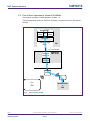
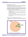
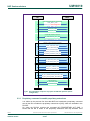
1
UM10819 PN7120 User Manual Rev. 1.0 — 3 April 2015 299610 User manual COMPANY PUBLIC Document information Info Content Keywords PN7120, NFC, NFCC, NCI Abstract This is a user manual for the PN7120 NFC Controller The aim of this document is to describe the PN7120 interfaces, modes of operation and possible configurations. UM10819 NXP Semiconductors PN7120 User Manual Revision history Rev Date Description 1.0 20150403 First official release 0.4 20150402 Modification of the chapter 13 about PRBS test mode 0.3 20150206 Revised version 0.2 20141223 Approved version 0.1 20140929 Initial version of the document Contact information For more information, please visit: http://www.nxp.com UM10819 User manual COMPANY PUBLIC All information provided in this document is subject to legal disclaimers. Rev. 1.0 — 3 April 2015 299610 © NXP Semiconductors N.V. 2015. All rights reserved. 2 of 120 UM10819 NXP Semiconductors PN7120 User Manual 1. Introduction The PN7120 is a full features NFC controller for contactless communication at 13.56 MHz. The User Manual describes the software interfaces (API), based on the NFC FORUM standard, NCI (see the chapter →17: References.) Note: this document includes cross-references, which can be used to directly access the section/chapter referenced in the text. These cross-references are indicated by the following sign: ‘→’. This sign is positioned right before the section/chapter reference. The way to jump to the referenced section/chapter depends on the file format: • In the word format, you have to first press the key “Ctrl” on the key board and then to click on the section/chapter reference number pointed by the ‘→’ sign. The mouse symbol changes to a small hand when it is positioned on the section/chapter reference number. • In .pdf format, you only have to click on the section/chapter reference number pointed by the ‘→’ sign : the mouse symbol automatically changes to a small hand when it is positioned on the section/chapter reference number As this document assumes pre-knowledge on certain technologies please check section →17: References to find the appropriate documentation. For further information please refer to the PN7120 data sheet [PN7120_DS]. UM10819 User manual COMPANY PUBLIC All information provided in this document is subject to legal disclaimers. Rev. 1.0 — 3 April 2015 299610 © NXP B.V. 2015. All rights reserved. 3 of 120 UM10819 NXP Semiconductors PN7120 User Manual 2. The PN7120 architecture overview The PN7120 is an NFC Controller, which is briefly described in Fig 1: • • • UM10819 User manual COMPANY PUBLIC The top part describes the Device Host (DH) architecture with Higher Layer Driver (i.e Android stack) hosting the different kind of applications (Reader/Writer, Peer to Peer, Card Emulation in the DH-NFCEE), the NCI driver & the transport layer driver. The PN7120 is the NFCC in the Fig 1. It is connected to the DH through a physical interface which is an I²C. The PN7120 firmware supports the NCI specification. The firmware also provides support for additional extensions that are not contained in the NCI specification. These additional extensions are specific to the PN7120 chip and are proprietary to NXP. The bottom part of the figure contains the RF antenna connected to the PN7120, which can communicate over RF with a Tag (Card) and a Reader/Writer or a Peer device. All information provided in this document is subject to legal disclaimers. Rev. 1.0 — 3 April 2015 299610 © NXP B.V. 2015. All rights reserved. 4 of 120 UM10819 NXP Semiconductors PN7120 User Manual DH-NFCEE Card Reader P2P Emulat° / Writer NCI driver Transport layer driver DH I²C1 host interface Transport Layer FW NFCC NCI firmware RF Antenna TAG or Card Fig 1. 1 Reader/Writer or P2P PN7120 system architecture No additional framing on I²C, → 4.3 For contactless operation, several Modes of operation are possible, based on the overall system described above. 2.1 Reader/Writer Operation in Poll Mode This mode of operation is further detailed in chapter →7. The Reader/Writer application running on the DH is accessing a remote contactless Tag/Card, through the PN7120. UM10819 User manual COMPANY PUBLIC All information provided in this document is subject to legal disclaimers. Rev. 1.0 — 3 April 2015 299610 © NXP B.V. 2015. All rights reserved. 5 of 120 UM10819 NXP Semiconductors PN7120 User Manual DH-NFCEE Reader Card P2P / Writer Emulat° NCI driver Transport layer driver DH I²C1 host interface Transport Layer FW NFCC NCI firmware RF Antenna TAG or Card Fig 2. 1 UM10819 User manual COMPANY PUBLIC Reader/Writer or P2P Reader/Writer hosted by the DH No additional framing on I²C, → 4.3 All information provided in this document is subject to legal disclaimers. Rev. 1.0 — 3 April 2015 299610 © NXP B.V. 2015. All rights reserved. 6 of 120 UM10819 NXP Semiconductors PN7120 User Manual 2.2 Card Emulation Operation in Listen Mode This mode of operation is further detailed in chapter →8. An external Reader/Writer accesses the DH-NFCEE emulating a contactless card, through the PN7120. DH-NFCEE Reader Card P2P / Writer Emulat° NCI driver Transport layer driver DH I²C1 host interface Transport Layer FW NFCC NCI firmware RF Antenna TAG or Card Fig 3. 1 UM10819 User manual COMPANY PUBLIC Reader/Writer or P2P Card Emulated by the DH-NFCEE No additional framing on I²C, → 4.3 All information provided in this document is subject to legal disclaimers. Rev. 1.0 — 3 April 2015 299610 © NXP B.V. 2015. All rights reserved. 7 of 120 UM10819 NXP Semiconductors PN7120 User Manual 2.3 Peer to Peer Operation in Listen & Poll Mode This mode of operation is further detailed in chapter →0 The P2P application running on the DH is accessing a remote Peer device, through the PN7120. DH-NFCEE Reader Card P2P / Writer Emulat° NCI driver Transport layer driver DH I²C1 host interface Transport Layer FW NFCC NCI firmware RF Antenna TAG or Card Fig 4. 1 UM10819 User manual COMPANY PUBLIC Reader/Writer or P2P P2P hosted by the DH No additional framing on I²C, → 4.3 All information provided in this document is subject to legal disclaimers. Rev. 1.0 — 3 April 2015 299610 © NXP B.V. 2015. All rights reserved. 8 of 120 UM10819 NXP Semiconductors PN7120 User Manual 2.4 Combined Modes of Operation The PN7120 firmware is able to combine the basic modes of operation described above, using the RF Discovery as defined in [NCI]. As the PN7120 offers more features than what [NCI] addressed, NXP has defined some proprietary extensions. The principle used to combine the various modes of operation is to build a cyclic activity which will sequentially activate various modes of operation. This cyclic activity is called the polling loop. This loop alternates listening phase (NFCC behaves as card or target) and polling phase (NFCC behaves as a reader/writer or an initiator). A cycle of the polling loop is called RF discovery sequence; it is made of 3 steps: 1. Start a Polling phase to look for a remote Tag/Card or a remote Target. If several technologies are enabled by the DH, PN7120 will poll sequentially for all the enabled technologies. 2. If no card or tag or target was detected, PN7120 enters a Listening phase, to potentially be activated as a Card / Tag emulator or a P2P target by an external Reader/Writer or external Initiator. 3. If no device to interact is detected during polling phase (step 1) or listening phase (step 2), then after a programmable timeout, PN7120 switches back to polling phase (step 1). A combination of the 3 different steps defines a polling loop profile. The RF discovery sequence is usually drawn as below (here applied for the NFC forum polling loop profile where technologies NFC-A, NFC-B & NFC-F are activated in Poll Mode): Listening phase NFC-A Polling phase NFC-B NFC-F Fig 5. UM10819 User manual COMPANY PUBLIC RF discovery sequence in case of NFC FORUM profile All information provided in this document is subject to legal disclaimers. Rev. 1.0 — 3 April 2015 299610 © NXP B.V. 2015. All rights reserved. 9 of 120 UM10819 NXP Semiconductors PN7120 User Manual Please note that when the PN7120 is in Poll phase, it consumes a significant amount of current: in the range of 30mA (depending on the antenna characteristics). This applies at least for the 3 polled technologies drawn on the Fig 5, above (NFC-A, NFC-B and NFC_F) and it is due to the fact that the PN7120 has to generate the RF carrier (13.56MHz). However, during the Listen phase, the PN7120 current consumption is reduced to around 20µA when standby mode is enabled, due to the fact that it is waiting for the detection of an externally generated RF carrier. Here is a figure illustrating a RF Discovery sequence, where polling is enabled only for NFC-A & NFC-B, for simplicity: One complete RF Discovery Sequence Listen Phase Poll Phase Poll A Listen Phase Poll B Poll Phase Poll A Listen Phase Poll B RF Field ~30 mA Current consumption ~20 µA ~20ms Fig 6. ~300ms Power consumption during RF discovery sequence in case of NFC forum profile In a typical set-up, the polling phase is approximately 20ms long while the listening phase is usually in the range 300ms to 500ms long (this is configured thanks to the NCI parameter called TOTAL_DURATION). For 500ms this gives an average power consumption of: [30x20 + 0.02x500] / 520 = 1.17mA. This average consumption can even be further optimized, using the PN7120 feature called “Tag Detector”. See chapter →10.3 for more details. See chapter →9.3 for further details on the RF discovery activity. UM10819 User manual COMPANY PUBLIC All information provided in this document is subject to legal disclaimers. Rev. 1.0 — 3 April 2015 299610 © NXP B.V. 2015. All rights reserved. 10 of 120 UM10819 NXP Semiconductors PN7120 User Manual 3. NCI Overview The aim of this section is to give an overview of the key points of the [NCI] specification. 3.1 NCI Components Here below are described the NCI component as defined in [NCI] which are located in the NFCC embedded FW. NFCEE Interfaces NFCEE Discovery RF Interfaces RF Discovery NCI modules (...) NCI Core Fig 7. Transport Mapping 1 Transport Mapping 2 Transport 1 Transport 2 (...) Transport Mapping n Transport n NCI components 3.1.1 NCI Modules NCI modules are built on top of the functionality provided by the NCI Core. Each module provides a well-defined functionality to the DH. NCI modules provide the functionality to configure the NFCC and to discover and communicate with Remote NFC Endpoints (see [NCI] for definition) or with DH-NFCEEs. Some NCI modules are mandatory parts of an NCI implementation, others are optional. There can also be dependencies between NCI modules in the sense that a module may only be useful if there are other modules implemented as well. For example all modules that deal with communication with a Remote NFC Endpoint (the RF Interface modules) depend on the RF Discovery to be present. 3.1.2 NCI Core The NCI Core defines the basic functionality of the communication between a Device Host (DH) and an NFC Controller (NFCC). This enables Control Message (Command, Response and Notification) and Data Message exchange between an NFCC and a DH. UM10819 User manual COMPANY PUBLIC All information provided in this document is subject to legal disclaimers. Rev. 1.0 — 3 April 2015 299610 © NXP B.V. 2015. All rights reserved. 11 of 120 UM10819 NXP Semiconductors PN7120 User Manual 3.1.3 Transport Mappings Transport Mappings define how the NCI messaging is mapped to an underlying NCI Transport, which is a physical connection (and optional associated protocol) between the DH and the NFCC. Each Transport Mapping is associated with a specific NCI Transport (see [NCI] for definition). 3.2 NCI Concepts This chapter outlines the basic concepts used in [NCI]. NFC Forum Device Data Messages Control Messages NFCEE Interface Control Messages RF Interface NCI Data Messages Control Messages DH NFCEE Protocol NFCEE RF Protocol NFCC Remote NFC Endpoint Fig 8. NCI concepts 3.2.1 Control Messages A DH uses NCI Control Messages to control and configure an NFCC. Control Messages consist of Commands, Responses and Notifications. Commands are only allowed to be sent in the direction from DH to NFCC, Responses and Notifications are only allowed in the other direction. Control Messages are transmitted in NCI Control Packets, NCI supports segmentation of Control Messages into multiple Packets. The NCI Core defines a basic set of Control Messages, e.g. for setting and retrieving of NFCC configuration parameters. NCI Modules can define additional Control Messages. UM10819 User manual COMPANY PUBLIC All information provided in this document is subject to legal disclaimers. Rev. 1.0 — 3 April 2015 299610 © NXP B.V. 2015. All rights reserved. 12 of 120 UM10819 NXP Semiconductors PN7120 User Manual DH NFCC Command Response Notification Control Message Exchange Fig 9. Control Message Exchange 3.2.2 Data Messages Data Messages are used to transport data to either a Remote NFC Endpoint (named RF Communication in NCI) or to an NFCEE (named NFCEE Communication). NCI defines Data Packets enabling the segmentation of Data Messages into multiple Packets. Data Messages can only be exchanged in the context of a Logical Connection. As a result, a Logical Connection must be established before any Data Messages can be sent. One Logical Connection, the Static RF Connection, is always established during initialization of NCI. The Static RF Connection is dedicated to be used for RF Communication. Additional Logical Connections can be created for RF and/or NFCEE Communication. Logical Connections provide flow control for Data Messages in the direction from DH to NFCC. DH NFCC Data DH NFCC Data Data Message Exchange Fig 10. Data Message Exchange UM10819 User manual COMPANY PUBLIC All information provided in this document is subject to legal disclaimers. Rev. 1.0 — 3 April 2015 299610 © NXP B.V. 2015. All rights reserved. 13 of 120 UM10819 NXP Semiconductors PN7120 User Manual 3.2.3 Interfaces An NCI Module may contain one Interface. An Interface defines how a DH can communicate via NCI with a Remote NFC Endpoint or NFCEE. Each Interface is defined to support specific protocols and can only be used for those protocols (the majority of Interfaces support exactly one protocol). NCI defines two types of Interfaces: RF Interfaces and NFCEE Interfaces. Protocols used to communicate with a Remote NFC Endpoint are called RF Protocols. Protocols used to communicate with an NFCEE are called NFCEE Protocols. An NFCEE Interface has a one-to-one relationship to an NFCEE Protocol, whereas there might be multiple RF Interfaces for one RF Protocol. The later allows NCI to support different splits of the protocol implementation between the NFCC and DH. An NCI implementation on an NFCC should include those RF Interfaces that match the functionality implemented on the NFCC. Interfaces must be activated before they can be used and they must be deactivated when they are no longer used. An Interface can define its own configuration parameters and Control Messages, but most importantly it must define how the payload of a Data Message maps to the payload of the respective RF or NFCEE Protocol and, in case of RF Communication, whether the Static RF Connection is used to exchange those Data Messages between the DH and the NFCC. 3.2.4 RF Communication RF Communication is started by configuring and running the polling loop (RF discovery sequences in loops). The RF discovery sequence involved the NCI module called RF discovery. This module discovers and enumerates Remote NFC Endpoints. For each Remote NFC Endpoint, the RF Discovery module provides the DH with the information about the Remote NFC Endpoint gathered during the RF Discovery sequence. One part of this information is the RF Protocol that is used to communicate with the Remote NFC Endpoint. During RF Discovery module configuration, the DH must configure a mapping that associates an RF Interface for each RF Protocol. If only a single Remote NFC Endpoint is detected during one discovery sequence, the RF Interface for this Endpoint is automatically activated. If there are multiple Remote NFC Endpoints detected during the Poll phase, the DH can select the Endpoint it wants to communicate with. This selection also triggers the activation of the mapped Interface. After an RF Interface has been activated, the DH can communicate with the Remote NFC Endpoint using the activated RF Interface. An activated RF Interface can be deactivated by either the DH or the NFCC (e.g. on behalf of the Remote NFC Endpoint). However each RF Interface can define which of those methods are allowed. Depending on which part of the protocol stack is executed on the DH there are different deactivation options. For example if a protocol command to tear down the communication is handled on the DH, the DH will deactivate the RF Interface. If such a command is handled on the NFCC, the NFCC will deactivate the Interface. This specification describes the possible Control Message sequences for RF Communication in the form of a state machine. UM10819 User manual COMPANY PUBLIC All information provided in this document is subject to legal disclaimers. Rev. 1.0 — 3 April 2015 299610 © NXP B.V. 2015. All rights reserved. 14 of 120 UM10819 NXP Semiconductors PN7120 User Manual 3.2.5 NFCEE Communication The DH can learn about the NFCEEs connected to the NFCC by using the NFCEE Discovery module. During NFCEE Discovery the NFCC assigns an identifier for each NFCEE. When the DH wants to communicate with an NFCEE, it needs to open a Logical Connection to the NFCEE using the corresponding identifier and specifying the NFCEE Protocol to be used. Opening a Logical Connection to an NFCEE automatically activates the NFCEE Interface associated to the protocol specified. As there is always a one-to-one relationship between an NFCEE Protocol and Interface, there is no mapping step required (different as for the RF Communication). After the Interface has been activated, the DH can communicate with the NFCEE using the activated Interface. Closing the connection to an NFCEE Interface deactivates that NFCEE Interface. NCI also includes functionality to allow the DH to enable or disable the communication between an NFCEE and the NFCC. 3.2.6 Identifiers The NFCC might only be used by the DH but also by the NFCEEs in the device (in such a case the NFCC is a shared resource). NFCEEs differ in the way they are connected to the NFCC and the protocol used on such a link determines how an NFCEE can use the NFCC. For example some protocols allow the NFCEE to provide its own configuration for RF parameters to the NFCC (similar to the NCI Configuration Parameters for RF Discovery) in other cases the NFCEE might not provide such information. NFCCs can have different implementation in how they deal with multiple configurations from DH and NFCEEs. They might for example switch between those configurations so that only one is active at a time or they might attempt to merge the different configurations. During initialization NCI provides information for the DH whether the configuration it provides is the only one or if the NFCC supports configuration by NFCEEs as well. NCI includes a module, called Listen Mode Routing, with which the DH can define where to route received data when the device has been activated in Listen Mode. The Listen Mode Routing allows the DH to maintain a routing table on the NFCC. Routing can be done based on the technology or protocol of the incoming traffic or based on application identifiers in case [7816-4] APDU commands are used on top of ISO-DEP. In case of PN7120 the only route is the DH-NFCEE, therefore no Listen Mode Routing programming supported. In addition NCI enables the DH to get informed if communication between an NFCEE and a Remote NFC Endpoint occurs. UM10819 User manual COMPANY PUBLIC All information provided in this document is subject to legal disclaimers. Rev. 1.0 — 3 April 2015 299610 © NXP B.V. 2015. All rights reserved. 15 of 120 UM10819 NXP Semiconductors PN7120 User Manual 3.3 NCI Packet Format 3.3.1 Common Packet Header All Packets have a common header, consisting of an MT field and a PBF field: 1 3 (bits) MT P B F Octet 0 Information Octet 1 - N Fig 11. NCI Core Packet Format Message Type (MT) The MT field indicates the contents of the Packet and SHALL be a 3 bit field containing one of the values listed in Table 1, below. The content of the Information field is dependent on the value of the MT field. The receiver of an MT designated as RFU SHALL silently discard the packet. Table 1. MT MT values Description 000b Data Packet 001b Control Packet - Command Message as a payload 010b Control Packet - Response Message as a payload 011b Control Packet – Notification Message as a payload 100b-111b RFU Packet Boundary Flag (PBF) The Packet Boundary Flag (PBF) is used for Segmentation and Reassembly and SHALL be a 1 bit field containing one of the values listed in [NCI] specification. Table 2. PBF PBF Value Description 0b The Packet contains a complete Message, or the Packet contains the last segment of a segmented Message 1b The Packet contains a segment of a Message which is not the last segment. The following rules apply to the PBF flag in Packets: UM10819 User manual COMPANY PUBLIC If the Packet contains a complete Message, the PBF SHALL be set to 0b. If the Packet contains the last segment of a segmented Message, the PBF SHALL be set to 0b. If the packet does not contain the last segment of a segmented Message, the PBF SHALL be set to 1b. All information provided in this document is subject to legal disclaimers. Rev. 1.0 — 3 April 2015 299610 © NXP B.V. 2015. All rights reserved. 16 of 120 UM10819 NXP Semiconductors PN7120 User Manual 3.3.2 Control Packets The Control Packet structure is detailed below. Packet Header 1 3 MT P B F Octet 0 4 GID 1 1 R F U R F U 6 8 OID Payload Length (L) Octet 1 Octet 2 L bytes Payload Octet 3... Octet (2+L) Fig 12. Control Packet Format Each Control Packet SHALL have a 3 octet Packet Header and MAY have additional payload for carrying a Control Message or a segment of Control Message. NOTE In the case of an ‘empty’ Control Message, only the Packet Header is sent. Message Type (MT) Refer to section 3.3.1 for details of the MT field. Packet Boundary Flag (PBF) Refer to section 3.3.1 for details of the PBF field. Group Identifier (GID) The NCI supports Commands, Responses and Notifications which are categorized according their individual groups. The Group Identifier (GID) indicates the categorization of the message and SHALL be a 4 bit field containing one of the values listed in [NCI] specification. All GID values not defined in [NCI] specification are RFU. Opcode Identifier (OID) The Opcode Identifier (OID) indicates the identification of the Control Message and SHALL be a 6 bit field which is a unique identification of a set of Command, Response or Notification Messages within the group (GID). OID values are defined along with the definition of the respective Control Messages described in [NCI] specification. Payload Length (L) The Payload Length SHALL indicate the number of octets present in the payload. The Payload Length field SHALL be an 8 bit field containing a value from 0 to 255. UM10819 User manual COMPANY PUBLIC All information provided in this document is subject to legal disclaimers. Rev. 1.0 — 3 April 2015 299610 © NXP B.V. 2015. All rights reserved. 17 of 120 UM10819 NXP Semiconductors PN7120 User Manual 3.3.3 Data Packets The Data Packet structure is detailed below. Packet Header 3 MT 1 4 P B F Conn ID Octet 0 8 L bytes Payload Length (L) Payload 8 RFU Octet 1 Octet 2 Octet 3 ... Octet (2+L) Fig 13. Data Packet Structure Each Data Packet SHALL have a 3 octet Packet Header and MAY have additional Payload for carrying a Data Message or a segment of a Data Message. NOTE: In the case of an ‘empty’ Data Message, only the Packet Header is sent. Message Type (MT) Refer to section 3.3.1 for details of the MT field. Packet Boundary Flag (PBF) Refer to section 3.3.1 for details of the PBF field. Connection Identifier (Conn ID) The Connection Identifier (Conn ID) SHALL be used to indicate the previously setup Logical Connection to which this data belongs. The Conn ID is a 4 bit field containing a value from 0 to 15. Payload Length (L) The Payload Length field indicates the number of Payload octets present. The Payload Length field is an 8 bit field containing a value from 0 to 255. UM10819 User manual COMPANY PUBLIC All information provided in this document is subject to legal disclaimers. Rev. 1.0 — 3 April 2015 299610 © NXP B.V. 2015. All rights reserved. 18 of 120 UM10819 NXP Semiconductors PN7120 User Manual 3.3.4 Segmentation and Reassembly The Segmentation and Reassembly functionality SHALL be supported by both the DH and the NFCC. Segmentation and Reassembly of Messages SHALL be performed independently for Control Packets and Data Packets of each Logical Connection. Any NCI Transport Mapping is allowed to define a fixed Maximum Transmission Unit (MTU) size in octets. If such a Mapping is defined and used, then if either DH or NFCC needs to transmit a Message (either Control or Data Message) that would generate a Packet (including Packet Header) larger than the MTU, the Segmentation and Reassembly (SAR) feature SHALL be used on the Message. The following rules apply to segmenting Control Messages: For each segment of a Control Message, the header of the Control Packet SHALL contains the same MT, GID and OID values. From DH to NFCC: the Segmentation and Reassembly feature SHALL be used when sending a Command Message from the DH to the NFCC that would generate a Control Packet with a payload larger than the “Max Control Packet Payload Size” reported by the NFCC at initialization. Each segment of a Command Message except for the last SHALL contain a payload with the length of “Max Control Packet Payload Size”. From NFCC to DH: when an NFCC sends a Control Message to the DH, regardless of the length, it MAY segment the Control Message into smaller Control Packets if needed for internal optimization purposes. The following rules apply to segmenting Data Messages: For each segment of a Data Message, the header of the Data Packet SHALL contain the same MT and Conn ID. UM10819 User manual COMPANY PUBLIC From DH to NFCC: if a Data Message payload size exceeds the Max Data Packet Payload Size, of the connection then the Segmentation and Reassembly feature SHALL be used on the Data Message. From NFCC to DH: when an NFCC sends a Data Message to the DH, regardless of the payload length it MAY segment the Data Message into smaller Data Packets for any internal reason, for example for transmission buffer optimization. All information provided in this document is subject to legal disclaimers. Rev. 1.0 — 3 April 2015 299610 © NXP B.V. 2015. All rights reserved. 19 of 120 UM10819 NXP Semiconductors PN7120 User Manual 4. DH interface 4.1 Introduction The I²C interface of the PN7120 is compliant with the I²C Bus Specification V3.0, including device ID and Soft Reset. It is slave-only, i.e. the SCL signal is an input driven by the host. ! NCI packets can be as long as 258 Bytes. If the DH I²C peripheral has a buffer limitation which is below 258 Bytes, then a fragmentation mechanism SHALL be used at the I²C transport layer, as defined in →4.7. The PN7120 I²C interface supports standard (up to 100kbps), fast-Speed mode (up to 400kbps) and High Speed mode (up to 3.4Mbit/s). I²C defines two different modes of addressing (7-bit & 10-bit). The PN7120 only supports the 7-bit addressing mode. Following names will be used in the document: Table 3. I2C pins correspondence I2C_ADDR0 Equivalent to pin I2C_ADR0 of the PN7120 when using I2C. SDA Equivalent to pin I2C_SDA_ of the PN7120 when using I2C. SCL Equivalent to pin I2C_SCL of the PN7120 when using I2C. The PN7120 I²C 7-bit address can be configured from 0x28 to 0x2B. The 2 least significant bits of the slave address are electrically forced by pin I2C_ADR0 So, in binary format, the PN7120 slave 7-bit address is: “0 1 0 1 0 0 I2C_ADDR0” Table 4. PN7120 I²C slave address Address Value I2C_ADDR0 Pin 0x28 0 0x29 1 This can be easily configured through direct connection of pin I2C_ADDR0 to either GND or PVDD at PCB level. 4.2 RF Booster PN7120 comes with a new feature which allows the connection of an external RF Booster to increase the RF Field generated on the Antenna. This RF Booster requires being Enabled/Disabled by the PN7120, therefore the BOOST_CTRL pin can be changed into a digital output pin used to drive the Enable input pin of the RF Booster. A configuration parameter is used to activate the control of the RF Booster Enable pin by PN7120 see parameter BOOSTER_CNTRL_CFG in →11.2.1. The value of this parameter has to be carefully managed since it may create electrical damages on the I2C_ADDR1 pin: UM10819 User manual COMPANY PUBLIC All information provided in this document is subject to legal disclaimers. Rev. 1.0 — 3 April 2015 299610 © NXP B.V. 2015. All rights reserved. 20 of 120 UM10819 NXP Semiconductors PN7120 User Manual • If there is no RF Booster connected to I2C_ADDR1 and this pin is connected either to GND or PVDD, then never configure BOOSTER_CNTRL_CFG different from value 0x00, otherwise there would be an electrical conflict between the voltage generated by PN7120 on this pin and the voltage externally forced on it. • If there is an RF Booster connected to the I2C_ADDR1, then never configure BOOSTER_CNTRL_CFG equal to value 0x00, since that would mean 2 input pins connected together and would lead to an undetermined voltage on this pins and would potentially generate parasitic current consumption on PVDD. If there is an RF Booster connected to the I2C_ADDR1 pin and the parameter BOOSTER_CNTRL_CFG is configured to a value different from 0x00, then the I²C Slave address is defined still by pin I2C_ADDR0 and a bit value which is set in the internal memory of PN7120, during manufacturing. By default, this bit emulates I2C_ADDR1 = '0'. 4.3 NCI Transport Mapping In the PN7120, there is no additional framing added for I²C: an NCI packet (either data or control message, as defined in chapter →3.3) is transmitted over I²C “as is”, i.e. without any additional Byte (no header, no CRC etc…). 4.4 Write Sequence from the DH As the I²C clock is mastered by the DH, only the DH can initiate an I²C exchange. A DH write sequence always starts with the sending of the PN7120 I²C Slave Address followed by the write bit (logical ‘0’: 0b). Then the PN7120 I²C interface sends an I²C ACK back to the DH for each data byte written by the DH. SDA I²C Stop SCL I²C Start It may send an I²C NACK (negative acknowledge) when none of the 3 buffers used by the NCI core in the PN7120 is free, which may happen in case PN7120 is in standby mode. If one single byte of a complete NCI frame is NACKed by the PN7120, the DH has to re-send the complete NCI frame and not only this single byte. I²C Slave Address + R/W bit = 0b NCI Header Byte 0 NCI Header Byte 1 NCI Payload Length NCI Payload Byte 0 NCI Payload Byte n-2 NCI Payload Byte n-1 NCI Payload Byte n IRQ Fig 14. I²C Write sequence ! It may happen that PN7120 has an NCI Message ready to be sent to the DH while it is receiving another NCI Message from the DH. In such a condition, the IRQ pin will be raised somewhere during the Write Sequence: this is not an error and has to be accepted by the DH: once the Write Sequence is completed, the DH has to start a Read Sequence (see →4.5). 4.5 Read Sequence from the DH The DH shall never initiate a spontaneous I²C read request. The DH shall wait until it is triggered by the PN7120. To trigger the DH, the PN7120 generates a logical transition UM10819 User manual COMPANY PUBLIC All information provided in this document is subject to legal disclaimers. Rev. 1.0 — 3 April 2015 299610 © NXP B.V. 2015. All rights reserved. 21 of 120 UM10819 NXP Semiconductors PN7120 User Manual from Low to High on its IRQ pin (if the IRQ pin is configured to be active High; see configuration chapter →11.1). So after writing any NCI command, the DH shall wait until the PN7120 raises its IRQ pin. The DH can then transmit a Read request to fetch the NCI answer from the PN7120. When the PN7120 needs to send a spontaneous notification to the DH (for instance an RF Interface activation notification), the PN7120 raises the IRQ pin and the DH performs a normal read as described above. A DH Read Sequence always starts by the sending of the PN7120 I²C Slave Address followed by the read bit (logical ‘1’). Then the DH I²C interface sends an ACK back to the PN7120 for each data Byte received. Figure 2 is an example where the IRQ is raised so the DH can proceed a read. DH knows how often to Apply the clock I²C Stop SDA I²C Start SCL If the DH sends more clocks, zeros will be sent I²C Slave Address NCI Header + R/W bit = 1b Byte 0 NCI Header Byte 1 NCI Payload Length NCI Payload Byte 0 NCI Payload Byte n-2 NCI Payload Byte n-1 NCI Payload Byte n IRQ If NFCC requests a transfer, but DH sets R/W bit to 0b, IRQ will remain high. NFCC requests a transfer All data has been read, IRQ is reset Fig 15. I²C Read sequence As indicated on the figure above, in case the PN7120 requests a data transfer by raising the IRQ pin and the DH tries to initiate a write sequence by positioning the write bit to 0b, the PN7120 keeps the IRQ active until the DH starts a read sequence. The DH is not allowed to proceed with a write sequence once the PN7120 has set the IRQ pin to its active value (logical ‘1’ in the figure above). If PN7120 has another message ready to be sent to the DH before the end of the ongoing Read Sequence, the IRQ pin will be first deactivated at the end of the on-going Read Sequence and then re-activated to notify to the DH that a new message has to be read. 4.6 Split mode The PN7120 supports the interruption of a frame transfer, as defined in [I²C]. This feature is only available in Read Mode; it is forbidden to use it in Write Mode. This can be useful in a system where the I²C bus is shared between several peripherals: it allows the host to stop an on-going exchange, to switch to another peripheral (with a different slave address) and then to resume the communication with the PN7120. Another typical use-case for the split mode is to have the DH reading first the NCI packet header, to know what the Payload length is. The DH can then allocate a buffer with an appropriate size and read the payload data to fill this buffer. This use-case is represented on the following picture: UM10819 User manual COMPANY PUBLIC All information provided in this document is subject to legal disclaimers. Rev. 1.0 — 3 April 2015 299610 © NXP B.V. 2015. All rights reserved. 22 of 120 UM10819 NXP Semiconductors PN7120 User Manual I²C Slave Address NCI Header Byte 0 + R/W bit = 1b NCI Header Byte 1 NCI Payload Length I²C Slave Address NCI Payload + R/W bit = 1b Byte 0 I²C Stop I²C Start I²C Stop SDA I²C Start DH can split the I²C Read transfer SCL NCI Payload Byte n IRQ Fig 16. I²C Read sequence with split mode 4.7 Optional transport fragmentation PN7120 comes with an optional transport fragmentation on I²C, which can be enabled/disabled thanks to bit b4 in IRQ_POLARITY_CFG (see →11.1). This fragmentation can only be used from the DH to the PN7120: there is no fragmentation available from the PN7120 to the DH! This fragmentation is purely implemented at the I²C transport layer and does not interfere with NCI segmentation, which remains possible on top. ! The I²C fragmentation implemented on PN7120 requires that the DH waits until it has received a Control Message of type Response in response to a Control Message of type Command before it can send any Data Message. The DH also has to wait until it has received a Credit Notification to release the credit consumed by a previous Data Message it has sent, before it can send a new Control Message of type Command. 4.7.1 Description of the I²C fragmentation: If the DH has limited capabilities to transport Frames of Bytes over I²C (so below the maximum frame size of an NCI packet which is equal to 258 Bytes), it SHALL send the NCI packet into several fragments, according to the following rules: • The fragment size has to be an integer multiple of 4 Bytes (excluding the Slave Address Byte required by the I²C protocol). • The minimum fragment size supported by the DH has to be long enough to transport the following sequence of commands, which is necessary to enable the feature by setting bit b4 in the IRQ_POLARITY_CFG parameter (see →11.1): − CORE_RESET_CMD − CORE_INIT_CMD − NCI_PROPRIETARY_ACT_CMD − CORE_SET_CONFIG_CMD • To implement a flow control mechanism, the DH has to follow the following sequence: − 1. The DH sends a first fragment of an NCI data packet. − 2. The DH waits for WaitTime = 500µs UM10819 User manual COMPANY PUBLIC All information provided in this document is subject to legal disclaimers. Rev. 1.0 — 3 April 2015 299610 © NXP B.V. 2015. All rights reserved. 23 of 120 UM10819 NXP Semiconductors PN7120 User Manual − 3. The DH writes the [Address & R/Wn] Byte over the I²C bus; it has then to check the I²C ACK bit generated by PN7120 : − 3a. if the ACK bit is not set, this means that PN7120 is still processing the previous fragment of the NCI packet and it is not yet ready to receive the next fragment. The DH has to wait for an additional WaitTime, moving back to step 2. − 3b. if the ACK bit is set, the DH can move to step 4. − 4. The DH transmits the next Fragment − 5. If the whole NCI packet has not yet been transmitted, the DH proceeds to step 2 with another fragment. If the whole NCI packet has been transmitted, the sequence is stopped. The next figure shows this sequence: UM10819 User manual COMPANY PUBLIC All information provided in this document is subject to legal disclaimers. Rev. 1.0 — 3 April 2015 299610 © NXP B.V. 2015. All rights reserved. 24 of 120 UM10819 NXP Semiconductors PN7120 User Manual DH sends the 1st Fragment DH waits for WaitTime = 500µs DH sends I²C [Addr & R/W] Byte Did NFCC acknowledge ? no yes DH writes the next fragment Is the NCI packet fully transmitted ? no yes Fig 17. I²C transport fragmentation algorithm, from DH point of view 4.7.2 Illustration of the I²C fragmentation: The 2 next figures illustrate a transfer of an NCI message implying I²C fragmentation, with a fragment size of 36 Bytes maximum, when: • The NCI message fits over a single NCI packet • The NCI message fits over multiple NCI packets (NCI segmentation is used on top of I²C fragmentation) UM10819 User manual COMPANY PUBLIC All information provided in this document is subject to legal disclaimers. Rev. 1.0 — 3 April 2015 299610 © NXP B.V. 2015. All rights reserved. 25 of 120 UM10819 NXP Semiconductors PN7120 User Manual Fig 18. I²C Fragmentation when 1 NCI message = 1 NCI packet Fig 19. I²C Fragmentation when 1 NCI message is segmented into NCI packets UM10819 User manual COMPANY PUBLIC All information provided in this document is subject to legal disclaimers. Rev. 1.0 — 3 April 2015 299610 © NXP B.V. 2015. All rights reserved. 26 of 120 UM10819 NXP Semiconductors PN7120 User Manual 5. Compliance to [NCI] and PN7120 extensions The PN7120 is a complex contactless System on Chip, which offers a lot of features. Unfortunately, [NCI] as defined by the NFC FORUM does not give full access to all these features. Therefore, NXP had to extend [NCI] with proprietary extensions, and the PN7120 DH interface which includes [NCI] plus the PN7120 extensions is referenced in the present document as [PN7120-NCI]. 5.1 Feature-based comparison of [NCI] and [PN7120-NCI] The table below represents the features overview of the PN7120. It highlights the main differences between the NCI standard ([NCI]) and [PN7120-NCI]. The Chapter column contains shortcuts to the section in the document where the feature is described in details. Table 5. Features overview Chapter Features [NCI] [PN7120-NCI] →10 RF Discovery activity (NFC FORUM, EMVCo) →7 Reader/Writer ISO-DEP for NFC-A & NFC-B, T1T, T2T, T3T, T4T →7 Reader/Writer MIFARE Classic, MIFARE Plus, ISO15693, Kovio →8 Card Emulation ISO-DEP for NFC-A & NFC-B →9.1 P2P passive (Initiator & Target) →9.2 P2P active (Initiator & Target) RF bit rates for Listen mode & Poll mode: →5.2.5 106kbps (NFC-A & NFC-B), 212kbps (NFC-F), 424kbps (NFC-F) →5.2.5 RF bit rates for Listen mode & Poll mode in techno NFC-A & NFC-B: 212kbps, 424kbps & 848kbps →11 Configuration: Power management, RF Settings, Clocking schemes Others: Presence check →7.1.3.3 Partially Covered Covered Not Covered 5.2 [NCI] Implementation in the PN7120 [NCI] defines several features which are optional or configurable. For instance, data exchange can use an optional flow control, for which the number of credits is defined by the NFCC. So the intent of this section is to describe those features in [NCI] which are optional or configured by the NFCC, to highlight how they are implemented in the PN7120. 5.2.1 Logical connections & credits Here is a simplified overview of an NFC Device as defined in the NFC FORUM: UM10819 User manual COMPANY PUBLIC All information provided in this document is subject to legal disclaimers. Rev. 1.0 — 3 April 2015 299610 © NXP B.V. 2015. All rights reserved. 27 of 120 UM10819 NXP Semiconductors PN7120 User Manual NFC Forum Device Control Messages NFCEE Interface Logical Connection Control Messages RF Interface NCI Logical Connection Control Messages DH RF Protocol NFCC Remote NFC Endpoint Fig 20. NFC FORUM Device architecture Logical connections are used to transport data between the DH and the NFCC. Although optional in [NCI], [PN7120-NCI] implements data flow control based on credits management. In order to minimize the required buffer/memory size, the number of credits is limited to 1 on each logical connection. The “Max Logical Connections” parameter reported in CORE_INIT_RSP equals 0x01 for [PN7120-NCI]. That means that when the DH needs to create a new logical connection, it has first to close the currently opened one, if any. Here is an overview of the logical connections & credits available in the PN7120: Table 6. Logical Connections/Credits configuration Number of Number of Logical connection connections credits Static RF connection 1 1 Max. Data Packet payload Size [32;255] 5.2.2 Compliance to [NCI] control messages Here is a detailed status, for the current version PN7120: Table 7. Status on the compliance to [NCI] control messages Group Control messages CORE UM10819 User manual COMPANY PUBLIC CORE_RESET_CMD / RSP / NTF CORE_INIT_CMD / RSP4 - 5 All information provided in this document is subject to legal disclaimers. Rev. 1.0 — 3 April 2015 299610 Status Partial Support1 Full Support © NXP B.V. 2015. All rights reserved. 28 of 120 UM10819 NXP Semiconductors PN7120 User Manual Group Control messages CORE_SET_CONFIG_CMD / RSP Full Support CORE_GET_CONFIG_CMD / RSP Full Support CORE_CONN_CREATE_CMD / RSP NFCEE Partial Support2 CORE_CONN_CLOSE_CMD / RSP Full Support CORE_CONN_CREDITS_NTF Full Support CORE_GENERIC_ERROR_NTF Full Support CORE_INTERFACE_ERROR_NTF Full Support RF_DISCOVER_MAP_CMD / RSP Full Support RF_SET_LISTEN_MODE_ROUTING_CMD / RSP Not supported RF_GET_LISTEN_MODE_ROUTING_CMD / RSP / NTF Not supported RF_DISCOVER_CMD / RSP / NTF RF Status Partial Support3 RF_DISCOVER_SELECT_CMD / RSP Full Support RF_INTF_ACTIVATED_NTF Full Support RF_DEACTIVATE_CMD / RSP / NTF Full Support RF_FIELD_INFO_NTF Full Support RF_T3T_POLLING_CMD / RSP / NTF Full Support RF_NFCEE_ACTION_NTF Full Support RF_NFCEE_DISCOVERY_REQ_NTF Full Support RF_PARAMETER_UPDATE_CMD / RSP Full Support NFCEE_DISCOVER_CMD / RSP / NTF Full Support NFCEE_MODE_SET_CMD / RSP Full Support 1 CORE_RESET_NTF has sometimes an additional field, not compliant to [NCI]. See 6.1. 2 The number of Destination Specific parameters is limited to 1. The Discovery Frequency parameter in RF_DISCOVER_CMD has no effect in PN7120; whatever the value written by the DH in this parameter, PN7120 will behave as if it is set to 0x01. 3 PN7120 wrongly declares in the "NFCC features" field of CORE_INIT_RSP that it supports the Discovery Frequency Configuration, although it does not. 4 PN7120 declares in the "RF Interfaces" field of CORE_INIT_RSP 0x81 and 0x82, which are RFU values. 5 ! PN7120 comes with a Maximum Control Packet Payload Size of 255 Bytes, as reported in the CORE_INIT_RSP. Since [NCI] defines that the maximum size of a Control Message is also 255 Bytes and that the DH has to completely fill a Control Packet when sending a long Control Message, Segmentation and Reassembly cannot be used by the DH with PN7120. 5.2.3 Compliance to [NCI] RF Interfaces Here is a drawing of the RF interfaces available in [NCI] and planned for “NCI Next Gen”: UM10819 User manual COMPANY PUBLIC All information provided in this document is subject to legal disclaimers. Rev. 1.0 — 3 April 2015 299610 © NXP B.V. 2015. All rights reserved. 29 of 120 UM10819 NXP Semiconductors PN7120 User Manual Fig 21. [NCI] RF Interface Architecture This section details the status on the different RF interfaces supported by the PN7120. Table 8. NCI Interface limitations RF Interface present in [NCI] Status Poll side Aggregated Frame RF interface No Support Poll side & Listen side Frame RF interface Partial Support1 Poll side & Listen side ISO-DEP interface Full support Poll side & Listen side NFC-DEP interface Full support 1 Frame RF Interface is not supported for P2P Passive & Active modes. 5.2.4 Compliance to [NCI] RF Discovery [NCI] relies on the [ACTIVITY] specification defined by the NFC FORUM. Since the P2P ACTIVE is not yet included in [ACTIVITY], the corresponding configuration parameters are mentioned as “RFU” in [NCI]. Since the PN7120 supports the P2P ACTIVE mode for both Initiator and Target roles, these parameters are actually used in [PN7120-NCI] 5.2.5 Compliance to [NCI] configuration parameters [NCI] defines a set of configuration parameters, in [NCI_Table8] (see chapter →17). Most of them are supported by PN7120; however, a subset of these parameters is not supported. Here is a status for all these parameters, together with their default value in PN7120: UM10819 User manual COMPANY PUBLIC All information provided in this document is subject to legal disclaimers. Rev. 1.0 — 3 April 2015 299610 © NXP B.V. 2015. All rights reserved. 30 of 120 UM10819 NXP Semiconductors PN7120 User Manual Config parameters Table 9. Compliance to [NCI] configuration parameters Status Coming from Default value Behavior if partial/no support TOTAL DURATION Partial Support [NCI] CON_DEVICE_LIMIT No Support [ACTIVITY] 0x03E8 (1s) Even if set for more, the total duration is limited to 2.57s 0x03 The PN7120 is using hard-coded values whatever the CON_DEVICE_LIMIT value is: - NFC-A: 3 - NFC-B: 1 - NFC-F: 2 - ISO15693: 2 - KOVIO: 1 PA_BAIL_OUT No Support [ACTIVITY] - PB_AFI Full support [DIGITAL] 0x00 PB_BAIL_OUT No Support [ACTIVITY] - PB_ATTRIB_PARAM1 Full support [DIGITAL] 0x00 PB_SENSB_REQ_ PARAM No Support [DIGITAL] - PF_BIT_RATE Full support [DIGITAL] 0x01 (212kbps) PF_RC_CODE Full support [DIGITAL] 0x00 PB_H_INFO Full support [DIGITAL] empty PI_BIT_RATE Full support [DIGITAL] 0x00 (106kbps) PA_ADV_FEAT No Support [DIGITAL] - PN_NFC_DEP_SPEED Full support [DIGITAL] 0x00 (106kbps) PN_ATR_REQ_GEN_BY TES Full support [DIGITAL] empty PN_ATR_REQ_CONFIG Full support [DIGITAL] 0x30 LA_BIT_FRAME_SDD Full support [DIGITAL] 0x01 LA_PLATFORM_CONFIG Full support [DIGITAL] 0x00 LA_SEL_INFO Full support [DIGITAL] 0x00 LA_NFCID1 Full support [DIGITAL] 0x08000000 LB_SENSB_INFO Full support [DIGITAL] 0x81 LB_NFCID0 Full support [DIGITAL] 0x08000000 LB_APPLICATION_DATA Full support [DIGITAL] Empty LB_SFGI Full support [DIGITAL] 0x00 LB_ADC_FO Full support [DIGITAL] 0x04 DID (CID) not supported by default LF_T3T_ IDENTIFIERS_1..16 No Support [DIGITAL] - No T3T card emulation in DH supported LF_PROTOCOL_TYP No Support [DIGITAL] - Always NFC-DEP LF_T3T_PMM No Support [DIGITAL] - No T3T card emulation in DH supported UM10819 User manual COMPANY PUBLIC Bail Out is always activated in Poll/NFC-A Bail Out is always activated in Poll/NFC-B No support of advanced features in NFC-B, no support of the extended SENSB_RES. !! the NCI mechanism to force the parameter to come back to its default value (CORE_SET_CONFIG with empty value) does not work for PF_RC_CODE!! No support of advanced features in NFC-A Warning! This value has to be changed to emulate a card in DH with ISO-DEP/NFC-A All information provided in this document is subject to legal disclaimers. Rev. 1.0 — 3 April 2015 299610 © NXP B.V. 2015. All rights reserved. 31 of 120 UM10819 NXP Semiconductors PN7120 User Manual Config parameters Status Coming from Default value Behavior if partial/no support LF_T3T_MAX Full support [NCI] 0x00 Value reported is always 0 (no T3T emulation in DH with PN7120) LF_T3T_FLAGS No Support [NCI] - No T3T card emulation in DH supported LF_CON_BITR_F No Support [DIGITAL] - Always both 212 & 424 kbps LF_ADV_FEAT No Support [DIGITAL] - No advanced features supported in NFC-F LI_FWI Full support [DIGITAL] 0x04 LA_HIST_BY Full support [DIGITAL] empty LB_H_INFO_RESP No Support [DIGITAL] - LI_BIT_RATE Full support [DIGITAL] 0x00 (106kbps) LN_WT Full support [DIGITAL] 0x08 LN_ATR_RES_GEN_BYT ES Full support [DIGITAL] Empty LN_ATR_RES_CONFIG Full support [DIGITAL] 0x30 RF_FIELD_INFO Full support [NCI] 0x00 RF_NFCEE_ACTION Full support [NCI] 0x01 NFCDEP_OP Full support [NCI] 0x0E Consequence: the "Higher Layer Response" field in the ATTRIB Response is left empty 5.2.6 Compliance to [NCI] data messages PN7120 is fully compliant to the [NCI] data messages. 5.3 Extensions added to [NCI] to allow full control of the PN7120 The [PN7120-NCI] Extensions section gives a quick overview of the numerous extensions required to [NCI] to give full access to all the features available in the PN7120. 5.3.1 [PN7120-NCI] extensions to [NCI] RF Protocols PN7120 supports much more protocols than handled today by [NCI]. It is required to extend the [NCI_Table5] defined in [NCI] (see chapter →17) such that these protocols can be configured in various commands/notifications: Table 10. Chapter UM10819 User manual COMPANY PUBLIC Proprietary RF protocols Value Description →7.1.4 →7.1.1 0x06 PROTOCOL_15693 0x80 PROTOCOL_MIFARE_CLASSIC 0x81-0x89 Reserved for Proprietary protocols →7.1.5 0x8A 0x8B-0x9F 0xA1-0xFD PROTOCOL_KOVIO Reserved for Proprietary protocols Reserved for Proprietary protocols All information provided in this document is subject to legal disclaimers. Rev. 1.0 — 3 April 2015 299610 © NXP B.V. 2015. All rights reserved. 32 of 120 UM10819 NXP Semiconductors PN7120 User Manual 5.3.2 [PN7120-NCI] extensions to [NCI] Bit Rates in ISO15693 and NFC-F PN7120 supports the Poll Mode for technology ISO15693. Unfortunately, [NCI] does not define an appropriate bit rate (26kbps) the NFCC has to report to the DH in the RF_INTF_ACTIVATED_NTF. NXP has defined a proprietary value for this bit rate. PN7120 offers the possibility to poll for NFC-F @ 212 kbps and NFC-F @ 424 kbps. unfortunately, [NCI] only allows configuring one of these 2 bit rates, but not both in the same discovery sequence. The [NCI] parameter used to configure the bit rate in NFC-F is PF_BIT_RATE; the values which can be applied to this parameter are defined in the [NCI_Table4] (see chapter →17). It is therefore required to extend this table such that the PN7120 is configured to poll during one discovery sequence for NFC-F @ 212 kbps and NFC-F @ 424 kbps. The proprietary value 0x80 is used for that purpose, and has to be restricted to technology NFC-F: Table 11. Chapter Proprietary Bit rates Value →7.1.4 5.3.3 0x80 Description NFC_BIT_RATE_26 [PN7120-NCI] extensions to [NCI] RF Interfaces PN7120 offers some features which are not accessible using the currently defined RF interfaces in [NCI]. So the [NCI_Table6] (see chapter →17) needs to be extended with some proprietary RF interfaces, as described in the table below: Table 12. Chapter Brief description TAG-CMD 0x80 This new interface adds a header to the data payload, in order to encode commands such as: _ T2T/MFUL sector select command _ MIFARE Classic Authenticate command - RFU 0x81 Reserved for proprietary RF Interfaces (Reported for debug purpose) - RFU 0x82 Reserved for proprietary RF Interfaces (Reported for debug purpose) 0x830xFE Reserved for proprietary RF Interfaces →7.1.1.2 5.3.4 RF Interfaces extension New RF Interface Value [PN7120-NCI] extensions to [NCI] Control messages This section contains all the additional commands/notifications in [PN7120-NCI]. Table 13. PN7120-NCI additional commands/notifications Chapter PN7120-NCI Control Brief description message Command used by the DH to activate the proprietary →6.3.1 NCI_PROPRIETARY_ ACT_CMD/RSP functions inside the NFCC Command used to check if a T4T or an ISO-DEP tag is still →7.1.3.3 RF_ PRES-CHECK_ CMD/RSP/NTF in the field. →11.3 RF_GET_TRANSITION_ To read out an RF register setting for a given RF CMD/RSP Transition →Error! SET_SCREEN_STATE_ To disable the Listen Modes routed to the DH (for Display Reference CMD/RSP Off/Display On implementation) source not found. UM10819 User manual COMPANY PUBLIC All information provided in this document is subject to legal disclaimers. Rev. 1.0 — 3 April 2015 299610 Support on PN7120 Full Support Full Support Full Support Full Support © NXP B.V. 2015. All rights reserved. 33 of 120 UM10819 NXP Semiconductors PN7120 User Manual Chapter →10.6.1 →10.4.3 →0 PN7120-NCI Control message CORE_SET_POWER_ MODE_CMD/RSP RF_TAG_DETECTOR_ TRACE_NTF TEST_PRBS_CMD/RSP Brief description Command allowing the DH to configure the power mode (standby or idle mode). Notification to collect the measurements performed by the Tag Detector Command allowing the DH to send data over RF at different baud rates in order to verify the contactless part without any interaction with the NCI RF Discovery. Support on PN7120 Full Support Full Support Full Support [NCI] defines some rules which constraint the use of the control messages. That means that depending on the state the NCI RF State Machine is in, depending on the RF Interface used, depending on some parameters, the control messages are valid or incorrect, and sometimes they trigger state transitions. NXP has extended these rules for the [PN7120-NCI] extensions. The following table gives a picture of these rules: UM10819 User manual COMPANY PUBLIC All information provided in this document is subject to legal disclaimers. Rev. 1.0 — 3 April 2015 299610 © NXP B.V. 2015. All rights reserved. 34 of 120 UM10819 NXP Semiconductors PN7120 User Manual CURRENT STATE RFST_IDLE Source Control Message parameter / RF Interface Next state NCI 1.0 CORE_RESET_CMD/RSP NCI 1.0 CORE_INIT_CMD/RSP NCI 1.0 CORE_SET_CONFIG_CMD/RSP NCI 1.0 CORE_GET_CONFIG_CMD/RSP NCI 1.0 NCI 1.0 NCI 1.0 NCI 1.0 NCI 1.0 NCI 1.0 NCI 1.0 NCI 1.0 CORE_CONN_CREATE_CMD/RSP CORE_CONN_CLOSE_CMD/RSP RF_DISCOVER_MAP_CMD/RSP RF_SET_LISTEN_MODE_ROUTING_CMD/RSP RF_GET_LISTEN_MODE_ROUTING_CMD/RSP RF_DISCOVER_CMD/RSP RF_DISCOVER_SELECT_CMD/RSP RF_DEACTIVATE_CMD/RSP/NTF* *: in states POLL_ACTIVE & LISTEN_ACTIVE NCI 1.0 RF_T3T_POLLING_CMD/RSP NCI 1.0 RF_PARAMETER_UPDATE_CMD/RSP NCI 1.0 NCI 1.0 NXP NXP NXP NXP NXP NXP NXP NXP parameters impacting the RF discovery other parameters parameters impacting the RF discovery other parameters NFCEE_DISCOVER_CMD/RSP NFCEE_MODE_SET_CMD/RSP SYSTEM_SET_POWER_MODE_CMD/RSP SYSTEM_PROPRIETARY_ACT_CMD/RSP SYSTEM_PRES-CHECK_CMD/RSP SYSTEM_GET_RF_TRANSITION_CMD/RSP SYSTEM_SET_SCREENSTATE_CMD/RSP TEST_PRBS_CMD/RSP TEST_ANTENNA_CMD/RSP TEST_SWP_CMD/RSP DISCOVERY Idle_Mode Sleep_Mode SleepAF_Mode Discovery Frame RF Interface other RF interface Frame RF Interface other RF interface RFST_DISCOVERY RFST_W4_ALL_DISC. RFST_W4_HOST_SELECT RFST_POLL_ACTIVE RFST_LISTEN_ACTIVE RFST_LISTEN_SLEEP Response STATUS Next state Response STATUS Next state Response STATUS Next state Response STATUS Next state Response STATUS Next state Response STATUS Next state Response STATUS Status_OK SEMANTIC Status_OK Status_OK Status_OK Status_OK Status_OK Status_OK Status_OK Status_OK Status_OK Status_OK SEMANTIC SEMANTIC SEMANTIC SEMANTIC SEMANTIC SEMANTIC SEMANTIC SEMANTIC SEMANTIC Status_OK Status_OK Status_OK Status_OK SEMANTIC Status_OK Status_OK Status_OK Status_OK Status_OK IDLE Status_OK SEMANTIC SEMANTIC SEMANTIC Status_OK Status_OK Status_OK Status_OK SEMANTIC SEMANTIC Status_OK Status_OK SEMANTIC Status_OK Status_OK Status_OK Status_OK SEMANTIC SEMANTIC SEMANTIC SEMANTIC Status_OK Status_OK SEMANTIC SEMANTIC SEMANTIC SEMANTIC SEMANTIC SEMANTIC SEMANTIC SEMANTIC IDLE Status_OK SEMANTIC SEMANTIC SEMANTIC Status_OK Status_OK Status_OK Status_OK SEMANTIC SEMANTIC SEMANTIC SEMANTIC SEMANTIC Status_OK Status_OK Status_OK Status_OK SEMANTIC SEMANTIC SEMANTIC SEMANTIC Status_OK Status_OK SEMANTIC SEMANTIC SEMANTIC SEMANTIC SEMANTIC SEMANTIC SEMANTIC SEMANTIC IDLE Status_OK SEMANTIC SEMANTIC SEMANTIC Status_OK Status_OK Status_OK Status_OK SEMANTIC SEMANTIC Status_OK Status_OK Status_OK Status_OK REJECTED REJECTED REJECTED SEMANTIC SEMANTIC SEMANTIC SEMANTIC Status_OK Status_OK SEMANTIC SEMANTIC SEMANTIC SEMANTIC SEMANTIC SEMANTIC SEMANTIC SEMANTIC IDLE Status_OK SEMANTIC SEMANTIC SEMANTIC Status_OK Status_OK Status_OK Status_OK SEMANTIC SEMANTIC Status_OK Status_OK SEMANTIC Status_OK Status_OK Status_OK Status_OK Status_OK SEMANTIC Status_OK SEMANTIC Status_OK Status_OK SEMANTIC SEMANTIC Status_OK SEMANTIC SEMANTIC SEMANTIC SEMANTIC SEMANTIC IDLE Status_OK SEMANTIC SEMANTIC SEMANTIC Status_OK Status_OK Status_OK Status_OK SEMANTIC SEMANTIC Status_OK Status_OK SEMANTIC Status_OK REJECTED REJECTED REJECTED SEMANTIC SEMANTIC Status_OK SEMANTIC Status_OK Status_OK SEMANTIC SEMANTIC SEMANTIC SEMANTIC SEMANTIC SEMANTIC SEMANTIC SEMANTIC IDLE Status_OK SEMANTIC SEMANTIC SEMANTIC Status_OK Status_OK Status_OK Status_OK SEMANTIC SEMANTIC Status_OK Status_OK SEMANTIC Status_OK REJECTED REJECTED REJECTED SEMANTIC SEMANTIC SEMANTIC SEMANTIC Status_OK Status_OK SEMANTIC SEMANTIC SEMANTIC SEMANTIC SEMANTIC SEMANTIC SEMANTIC SEMANTIC IDLE IDLE IDLE IDLE IDLE IDLE IDLE IDLE IDLE IDLE W4_HOST_SELECT W4_HOST_SELECT DISCOVERY IDLE IDLE Fig 22. CMDs/RSPs versus the current state of the NCI RF State Machine UM10819 User manual PUBLIC All information provided in this document is subject to legal disclaimers. COMPANY Rev. 1.0 — 3 April 2015 299610 © NXP B.V. 2015. All rights reserved. 35 of 120 UM10819 NXP Semiconductors PN7120 User Manual PN7120 defines additional states to the RF state machine defined in [NCI_Chap2], to ensure a correct implementation of the “atomic behavior” of the pair of commands made by CORE_RESET_CMD & CORE_INIT_CMD and also to correctly handle wrong RF protocol to RF interface mapping through the RF_DISCOVER_MAP_CMD. The drawing below illustrates these additional states, linked to the [NCI]-defined RFST_IDLE: HW Reset BOOT_IDLE CORE_RESET_CMD/RSP BOOT_RESET CORE_INIT_CMD/RSP CORE_RESET_CMD/RSP RFST_IDLE RF_DISCOVER_MAP_RSP (STATUS_REJECTED) RF_DISCOVER_MAP_RSP (STATUS_OK) W4_CORRECT MAPPING Fig 23. States added to the [NCI] State Machine. 5.3.5 [PN7120-NCI] extensions to [NCI] Configuration parameters [NCI] lists a number of parameters, which are necessary to set up the RF discovery. But the PN7120 requires a lot more parameters, for instance to configure some RF protocols which are not supported by [NCI], to configure the power & clock management etc… Here is a list of sets of parameters, sorted out by features to configure: UM10819 User manual COMPANY PUBLIC All information provided in this document is subject to legal disclaimers. Rev. 1.0 — 3 April 2015 299610 © NXP Semiconductors N.V. 2015. All rights reserved. 36 of 120 UM10819 NXP Semiconductors PN7120 User Manual Table 14. Overview of additional Configuration parameters Chapter Feature to configure Comment →11.1 System →11.2 RF Discovery →11.3 Contactless Front-End Parameters allowing the DH to configure the System: Clock management, IRQ and CLOCKREQ pins management, MIFARE Classic Keys handling… Parameters allowing the DH to configure the Discovery activity (Tag Detector, Discovery profile between: NFC FORUM, NFC FORUM+ and EMVCo etc…). Parameters allowing the DH to configure all internal HW settings in the Contactless InterFace (CIF). Please refer to the chapters listed in the first column to have all the detailed information on the parameters. 5.3.6 [PN7120-NCI] extensions to [NCI] proprietary parameters space [NCI] defines a parameter space with a size of 255 parameters, in which around 100 tags are allocated for proprietary parameters: Table 15. Parameter space Parameters space sub-sections Tag Assigned & reserved for NCI 1.0 0x00-0x9F Reserved for Proprietary Use 0xA0-0xFE RFU (Reserved for Extension) 0xFF Regarding the PN7120 needs, this reserved area is not sufficient. To extend this space, the solution chosen is to define a space of Tags coded on 16 bits, instead of 8 bits. These extended Tags will always start by the value 0xA0, which is the first value available in the Proprietary range. This allows adding 256 new parameters. Remark: If this is not sufficient in the future, we might use 16-bit tag values starting by 0xA1, 0xA2 etc… Table 16. Extended TLV for proprietary parameters Payload Field Length Description m+3 Octets Tag = 0xA0XX 2 Octet Len 1 Octet Val m Octets Extended tag identifier. The length of Val (m). Value of the configuration parameter. This is illustrated by the following picture: UM10819 User manual COMPANY PUBLIC All information provided in this document is subject to legal disclaimers. Rev. 1.0 — 3 April 2015 299610 © NXP Semiconductors N.V. 2015. All rights reserved. 37 of 120 UM10819 NXP Semiconductors PN7120 User Manual 1 octet 1 octet x octets Lena Taga Vala 2 octets 1 octet y octets 1 octet 1 octet z octets Tagb= 0xA0XX Regular TLV Lenb Taga Valb Extended TLV Lena Vala Regular TLV Fig 24. Regular & Extended TLVs comparison 5.3.7 [PN7120-NCI] extensions to [NCI] Status Codes [NCI] defines a set of standard Status Codes in [NCI_Table1] (see chapter →17). NXP has extended this set of status codes with the following values: Table 17. Proprietary Status Codes Status code Description 5.3.8 Used in 0xE0 STATUS_DO_NOT_REPLY CORE_GENERIC_ERROR_NTF 0xE1 STATUS_BOOT_TRIM_CORRUPTED CORE_GENERIC_ERROR_NTF 0xE2 STATUS_PMU_DCDC_OVERLOAD CORE_GENERIC_ERROR_NTF 0xE3 STATUS_PMU_TXLDO_OVERCURRENT CORE_GENERIC_ERROR_NTF 0xE4 STATUS_EMVCO_PCD_COLLISION CORE_GENERIC_ERROR_NTF [PN7120-NCI] extensions to [NCI] Reason Code in CORE_RESET_NTF [NCI] defines a set of standard Reason Codes in the CORE_RESET_NTF. Please refer to [NCI_Table9] (see chapter →17). NXP has extended this set of reason codes with the following value: Table 18. Proprietary Reason Codes in CORE_RESET_NTF Reason Code Description 0xA0 An assert has triggered PN7120 reset/reboot 0xA1 An over temperature has triggered the reset of PN7120 0xA2 The current limiter has been triggered on the SVDD supply 0xA3 ARM sub-system reset / Watchdog reset has occurred ! When the 0xA0 Reason Code is used, the CORE_RESET_NTF is out of [NCI] compliance. Indeed, PN7120 appends one parameter at the end of the CORE_RESET_NTF, to provide some information for debug purposes. The CORE_RESET_NTF format is then: Table 19. CORE_RESET_NTF when reason code = 0xA0 is used Payload Field(s) Length Description UM10819 User manual COMPANY PUBLIC Reason Code 1 Octet 0xA0: NXP proprietary Config. Status 1 Octet See [NCI] All information provided in this document is subject to legal disclaimers. Rev. 1.0 — 3 April 2015 299610 Default 0xA0 © NXP Semiconductors N.V. 2015. All rights reserved. 38 of 120 UM10819 NXP Semiconductors PN7120 User Manual Payload Field(s) Length Description Default dwAssertionProgramCounter 4 Octets Program counter for assertion Here are the known address for assertion: · 0x0000d4d6: No clock is present to start TxLDO. · 0x00008d82 / 0x00008db8: Process message box full Here is the sequence followed by PN7120 when an over temperature is detected (Reason Code = 0xA1): • PN7120 forces pins CLK_REQ to logical '0' • PN7120 waits then until the chip temperature comes down to an internal threshold (the power consumption in this mode is around 100µA, since the temperature monitoring circuit is still alive) • When the internal temperature is low enough, PN7120 reboots, disabling the RF discovery if it was previously enabled • PN7120 sends then a CORE_RESET_NTF(0xA1) to inform the DH that an over temperature event occurred. 5.3.9 [PN7120-NCI] extensions to [NCI] RF Technology & Mode PN7120 supports more RF Technology & Mode parameters than handled today by [NCI]. It is required to extend the [NCI_Table3] defined in [NCI] (see chapter →17) such that these RF Technology & Mode parameters can be used in RF_DISCOVER_CMD: Table 20. Chapter Proprietary RF Technology & Mode parameters Value Description →7.1.5 UM10819 User manual COMPANY PUBLIC 0x77 NFCA_KOVIO_POLL_MODE 0x71-0x76 0x78-0x7F Reserved for Proprietary Technologies in Poll Mode All information provided in this document is subject to legal disclaimers. Rev. 1.0 — 3 April 2015 299610 © NXP Semiconductors N.V. 2015. All rights reserved. 39 of 120 UM10819 NXP Semiconductors PN7120 User Manual 6. Initialization & Operation configuration 6.1 Reset / Initialization [NCI] defines a Reset/Init sequence, which is based on two different commands: CORE_RESET_CMD CORE_INIT_CMD These two commands have to be called by the DH in an “atomic” way: there cannot be any other command in-between and the PN7120 operation cannot start any operation (Reader/Writer, Card Emulation, P2P, Combined modes etc…) if it does not first receive these 2 commands. [NCI] defines 2 modes for the Reset command: Keep Configuration & Reset Configuration. Here is the detail of the difference between the 2 reset modes: Table 21. Comparison of the 2 Reset Modes Features CPU reboot NCI Configuration parameters Proprietary Configuration parameters Interface Mapping Table Discovery activity ! Reset Configuration Keep Configuration Yes Back to default Kept Lost Lost Yes Kept Kept Kept Lost PN7120 may delay the CORE_RESET_RSP If the DH sends a CORE_RESET_CMD while PN7120 has already indicated that it has some data available to be read by the DH (IRQ pin activated), the DH has first to read the data available from PN7120 before it can get the CORE_RESET_RSP. The reason is that the NCI output buffer in PN7120 needs to be flushed before PN7120 can apply a Reset and then send the CORE_RESET_RSP. 6.2 Manufacturer Specific Information in [NCI] CORE_INIT_RSP The NCI command CORE_INIT_RSP contains a field “Manufacturer Specific Information” with 4 bytes. Here are the values of these 4 Bytes: Table 22. Manufacturer specific information in CORE_INIT_RSP Byte Meaning Condition to increment 0 1 2 3 Hardware Version number ROM Code Version number Firmware Major version Firmware Minor version 0x05 0x08 0x02 0x02 6.3 Whole sequence to prepare the PN7120 operation After the Reset/Init sequence is passed, the PN7120 requires several other steps before it is ready to start operating as a Reader/Writer, Card Emulator etc… UM10819 User manual COMPANY PUBLIC All information provided in this document is subject to legal disclaimers. Rev. 1.0 — 3 April 2015 299610 © NXP Semiconductors N.V. 2015. All rights reserved. 40 of 120 UM10819 NXP Semiconductors PN7120 User Manual The simplest case is when the DH issues a CORE_RESET_CMD with Reset Type = Keep Configuration. On this figure, Green background means mandatory exchange DH NFCC Reset / Init Sequence (atomic, cannot be split) CORE_RESET_CMD (Reset Type = Keep Configuration) CORE_RESET_RSP CORE_INIT_CMD CORE_INIT_RSP Activate NXP proprietary extensions NCI_PROPRIETARY_ACT_CMD NCI_PROPRIETARY_ACT_RSP Start RF Discovery RF_DISCOVER_CMD RF_DISCOVER_RSP Fig 25. Initialization sequence to prepare the PN7120 operation (Keep Configuration) Now, here is the figure which lists the complete sequence, starting by a Reset Command based on Reset Type = Reset Configuration. Since the entire configuration is lost, the PN7120 needs to be reconfigured and various optional steps are added, which might be needed or not, depending on the use case. On this figure, Green background means mandatory exchange Blue background means optional exchange, depending on the use case. UM10819 User manual COMPANY PUBLIC All information provided in this document is subject to legal disclaimers. Rev. 1.0 — 3 April 2015 299610 © NXP Semiconductors N.V. 2015. All rights reserved. 41 of 120 UM10819 NXP Semiconductors PN7120 User Manual NFCC DH Reset / Init Sequence (atomic, cannot be split) CORE_RESET_CMD (Reset Type = Reset Configuration) CORE_RESET_RSP CORE_INIT_CMD CORE_INIT_RSP Activate NXP proprietary extensions NCI_PROPRIETARY_ACT_CMD NCI_PROPRIETARY_ACT_RSP Optional: if system includes some NFCEEs NFCEE_DISCOVER_CMD NFCEE_DISCOVER_RSP NFCEE_DISCOVER_NTF RF_NFCEE_DISCOVERY_REQ_NTF RF_NFCEE_DISCOVERY_REQ_NTF Optional: if Protocol to RF Interface default mapping does not fit RF_DISCOVER_MAP_CMD RF_DISCOVER_MAP_RSP Optional: if default RF parameters need to be modifed CORE_SET_CONFIG_CMD CORE_SET_CONFIG_RSP Optional: Load the Listen Mode Routing Table RF_SET_LISTEN_MODE_ROUTING_CMD RF_SET_LISTEN_MODE_ROUTING_RSP Start RF Discovery RF_DISCOVER_CMD RF_DISCOVER_RSP Fig 26. Full initialization sequence to prepare the PN7120 operation (Reset configuration) 6.3.1 Proprietary command to enable proprietary extensions It is visible on the previous flow chart that NXP has introduced a proprietary command sent by the DH to enable the proprietary extensions to [NCI], which are available in the PN7120. So, when the PN7120 receives this command NCI_PROPRIETARY_ACT_CMD, it knows that the DH is aware of the proprietary extensions and may therefore send UM10819 User manual COMPANY PUBLIC All information provided in this document is subject to legal disclaimers. Rev. 1.0 — 3 April 2015 299610 © NXP Semiconductors N.V. 2015. All rights reserved. 42 of 120 UM10819 NXP Semiconductors PN7120 User Manual proprietary notifications (see the list in Table 12). If the PN7120 does not receive this proprietary command, it knows that the DH do not understand proprietary extensions and will therefore not send any proprietary notifications. Here is the description of this command: Table 23. GID 1111b 0x02 Table 24. GID 1111b NCI_PROPRIETARY_ACT_CMD Numbers of OID Description parameter(s) 0 DH informs the PN7120 that it knows the proprietary extensions. NCI_PROPRIETARY_ACT_RSP Numbers of OID Description parameter(s) 0x02 2 PN7120 indicates that it understood the command. Table 25. NCI_PROPRIETARY_ACT_RSP parameters Payload Field(s) Length Value/Description STATUS 1 Octet FW_Build_Number One of the following Status codes, as defined in [NCI_Table1] 0x00 STATUS_OK 0x03 STATUS_FAILED Others Forbidden 4 Octets NXP internal firmware build number 6.3.2 Configuration template In order to help the user of the PN7120 to issue the right configuration sequence for a given mode of operation, the present document will detail a typical configuration sequence, based on the following template: Table 26. Template for a typical configuration sequence Command Main Parameters RF_DISCOVER_MAP_CMD CORE_SET_CONFIG_CMD RF_DISCOVER_CMD Values RF Protocol Mode RF Interface Depends on technology & mode RF Technology & Mode … … … … … 6.4 PLL input Clock Management The PN7120 is flexible in terms of clock sources. It can be either: UM10819 User manual COMPANY PUBLIC a 27.12MHz quartz or a clean clock signal available on the platform on which PN7120 is connected. A PLL inside PN7120 will convert this input clock signal into an internal 27.12MHz used to generate the RF carrier. The input clock frequency has to be one of the predefined set of input frequencies: 13MHz, 19.2MHz, 24MHz, 26MHz, 38.4MHz and 52MHz. All information provided in this document is subject to legal disclaimers. Rev. 1.0 — 3 April 2015 299610 © NXP Semiconductors N.V. 2015. All rights reserved. 43 of 120 UM10819 NXP Semiconductors PN7120 User Manual The DH has to configure the parameter CLOCK_SEL_CFG (see chapter →11.1) to configure what is the clock source as used in the current application. Table 27. Name Clock sources supported Description XTAL To be selected when a 27.12MHz quartz is used as a clock source PLL To be selected when an input clock is provided to PN7120, with a frequency equal to either 13MHz, 19.2MHz, 24MHz, 26MHz, 38.4MHz or 52MHz The same parameter (CLOCK_SEL_CFG) is used to configure which clock frequency is used as an input to the PLL when this is the clock source in use. In order to optimize system power consumption, it may be required to switch OFF the PLL input clock when the PN7120 does not have to generate the 13.56MHz RF carrier or download a new firmware. A dedicated pin (CLKREQ) is used to inform the DH or a clock generating chip that the PN7120 requires to get the PLL input clock, such that it can generate the 13.56MHz RF carrier. PN7120 assumes that the PLL input clock is On and stable after a programmable timeout, which is configured thanks to the parameter CLOCK_TO_CFG (see chapter →11.1). 7. Poll side: Reader/Writer Mode 7.1 Reader/Writer hosted by the DH 7.1.1 T1T, T2T, MIFARE Ultralight, MIFARE Classic & MIFARE Plus tags Note : all the Tags/Cards in this category are based on NFC-A technology, but they do not support the ISO-DEP Protocol. MIFARE Plus cards support the ISO-DEP protocol, but only when they are configured in Security Level3, which is out of scope for this section. 7.1.1.1 Access through the [NCI] Frame RF Interface [NCI] allows the data exchange with tags T1T, T2T using the Frame RF Interface. Most of the commands of the MIFARE Classic & MIFARE Plus can also be mapped on the Frame RF Interface, but NXP decided to use a separate RF interface (TAG-CMD, see →7.1.1.2) because some MIFARE Classic commands are split in 2 steps (e.g. Authenticate command) and has a tight response timeout (1ms) which can hardly be monitored by the DH through the PN7120. Here is a summary of the Tags/Card based on technology NFC-A which can be accessed through the Frame RF interface Table 28. Tag/Cards accessible over the [NCI] Frame RF Interface Access through the Frame Tag/Card RF Interface UM10819 User manual COMPANY PUBLIC T1T T2T MIFARE Ultralight, Ultralight C MIFARE Classic All information provided in this document is subject to legal disclaimers. Rev. 1.0 — 3 April 2015 299610 © NXP Semiconductors N.V. 2015. All rights reserved. 44 of 120 UM10819 NXP Semiconductors PN7120 User Manual Access through the Frame RF Interface Tag/Card MIFARE Plus for Security levels 1 & 2 Here are the commands and configuration parameters to prepare the Reader/Writer Mode for T1T & T2T through the Frame RF Interface: Table 29. Configuration seq. for Reader/Writer of T1T or T2T through the Frame RF Intf Command Main Parameters Values RF_DISCOVER_MAP_CMD* CORE_SET_CONFIG_CMD RF_DISCOVER_CMD RF Protocol PROTOCOL_T1T (choose between the 2 possible PROTOCOL_T2T protocols) Mode Poll RF Interface Frame RF Interface PA_BAIL_OUT* RF Technology & Mode NFC_A_PASSIVE_POLL_MOD E * Note : RF_DISCOVER_MAP_CMD is optional since the mapping to Frame RF Intf. is done by default * this parameter is not active in PN7120 : it can be read/written, but PN7120 will always behave with Bail Out in NFC-A, whatever the value written by the DH to that parameter. 7.1.1.2 [PN7120-NCI] extension: TAG-CMD Interface The figure bellow represents the location of the TAG-CMD RF Interface: Fig 27. TAG-CMD RF Interface UM10819 User manual COMPANY PUBLIC All information provided in this document is subject to legal disclaimers. Rev. 1.0 — 3 April 2015 299610 © NXP Semiconductors N.V. 2015. All rights reserved. 45 of 120 UM10819 NXP Semiconductors PN7120 User Manual 7.1.1.3 [PN7120-NCI] extension: Payload structure of the TAG-CMD RF Interface The TAG-CMD RF Interface is using the same data mapping as the one defined for the [NCI] Frame RF Interface (see section 8.2.1 in [NCI]). However, for the TAG-CMD RF Interface, the Payload is defined differently. Two different structures are defined: 1. REQ (requests) : these are commands from the DH to the PN7120 2. RSP (responses): these are responses from the PN7120 to the DH. The diagram below details how the Payload is modified to insert a header, which carries the REQ ID or the RSP ID and some parameters, if required. Byte 0 NCI data packet structure Msg Conn ID Type Byte 0 REQs Frame structure Msg Conn ID Type Byte 0 RSPs Frame structure Msg Conn ID Type Byte 1 Byte 2 RFU Payload Length Byte 1 Byte 2 Byte 3 Byte 4 Byte 5 RFU Payload Length REQ ID Parameter 1 (optional) Parameter 2 (optional) Byte 1 Byte 2 Byte 3 RFU Payload Length RSP ID PAYLOAD DATA (if any) Byte n DATA (if any) RF Status Fig 28. Data message payload for the TAG-CMD Interface Note: REQs and RSPs don’t share exactly the same structure: REQs: Although illustrated with 2 parameters on the figure above, REQs may have no parameters or only one. Some REQuests might also need parameters bigger than 1 Byte. Parsing The REQ ID is the way to know how many parameters follow and how long they are. RSPs: there are no parameters in ReSPonses. A Byte is added at the end of the payload (after the DATA field) to inform the DH on the RF status (to report RF errors if they were some). The Status codes used are the following: Table 30. TAG-CMD RF Status code Value Description 0x00 STATUS_OK 0x03 STATUS_FAILED 0xB0 RF_TRANSMISSION_ERROR 0xB1 RF_PROTOCOL_ERROR 0xB2 RF_TIMEOUT_ERROR Others UM10819 User manual COMPANY PUBLIC Forbidden All information provided in this document is subject to legal disclaimers. Rev. 1.0 — 3 April 2015 299610 © NXP Semiconductors N.V. 2015. All rights reserved. 46 of 120 UM10819 NXP Semiconductors PN7120 User Manual 7.1.1.4 [PN7120-NCI] extension: REQs & RSPs rules A REQ command is always going from DH to RF, through the PN7120. A RSP response is always going from the RF to the DH, through the PN7120 The DH SHALL wait until it has received a RSP associated to a REQ before it can send a new REQ. 7.1.1.5 [PN7120-NCI] extension: List of REQs & RSPs In this section, the following acronyms are used: Table 31. Acronyms definition Acronym Description T1T NFC FORUM Type 1 Tag (based on Topaz/Jewel) MF MIFARE family, not ISO-DEP compliant, including T2T, MIFARE Ultra-Light (std or C), MIFARE Classic and MIFARE Plus for Security Level 1 & 2. MFC UM10819 User manual COMPANY PUBLIC MIFARE Classic and MIFARE Plus for Security Level 1 & 2. All information provided in this document is subject to legal disclaimers. Rev. 1.0 — 3 April 2015 299610 © NXP Semiconductors N.V. 2015. All rights reserved. 47 of 120 UM10819 NXP Semiconductors PN7120 User Manual The added REQuests/ReSPonses pairs are listed in the following table: Table 32. List of REQuests & ReSPonses ID Param 1 Param 2 Param 3 Data Description REQ/RSP Name XCHG_DATA_REQ None None None Yes 0x10 MFC: DH sends Raw data to the PN7120, which encrypts them before sending them to MFC. T1T/T2T: DH sends Raw data to the PN7120, which forwards them in plain to the Tag. XCHG_DATA_RSP N/A N/A N/A Yes 0x10 MF_SectorSel_REQ 0x32 MF_SectorSel_RSP 0x32 MFC: DH gets Raw data once RF data from MFC are decrypted by the PN7120, if successful. T1T/T2T: DH gets Raw plain data once the PN7120 receives RF data from the Tag, if successful. Sector Address None None No T2T & MFU only: DH Sends the address of the Block to select. N/A N/A N/A No T2T & MFU only: DH gets the “Sector Select” response status Key (optional) No DH asks PN7120 to perform MFC Authenticate command. No DH gets the MFC Authenticate command status MFC_Authenticate_REQ 0x40 Sector Address Key Selector MFC_Authenticate_RSP 0x40 N/A N/A All these REQs & RSPs are detailed in the next sections. 7.1.1.6 [PN7120-NCI] extension: raw data exchange REQs & RSPs Table 33. REQ_ID REQ Name XCHG_DATA_REQ Number of Presence Description parameter(s) of data XCHG_DATA_REQ 0 Yes 0x10 T1T/T2T: DH sends Raw data to the PN7120, which forwards them in plain to the Tag. Table 34. RSP_ID MFC: DH sends Raw data to the PN7120, which encrypts them before sending them to MFC. RSP Name XCHG_DATA_RSP 0x10 UM10819 User manual COMPANY PUBLIC XCHG_DATA_RSP Presence Description of Data Yes MFC: DH gets Raw data once RF data from MFC are decrypted by the PN7120, if successful. T1T/T2T: DH gets Raw plain data once the PN7120 receives RF data from the Tag, if successful. If the response from the MF tag in the field is an ACK or a NACK, the ACK/NACK is also sent back to the DH inside the Data field. Since ACK & NACK are 4-bit commands, they are transported on the 4 LSBs of the data Byte; the 4MSBs of that Byte are forced to the logical ‘0’ value. All information provided in this document is subject to legal disclaimers. Rev. 1.0 — 3 April 2015 299610 © NXP Semiconductors N.V. 2015. All rights reserved. 48 of 120 UM10819 NXP Semiconductors PN7120 User Manual 7.1.1.7 [PN7120-NCI] extension: T2T & MFU REQs & RSPs All the REQs & RSPs described in this section can be used whatever the tag between: T2T MIFARE Ultralight (std or C) Table 35. REQ_ID REQ Name 0x32 MF_SectorSel_REQ Table 36. 1 MF_SectorSel_REQ Number of Presence Description parameter(s) of data 1 MF_SectorSel_REQ parameter Length Parameter (Byte) Sector Address No Value 1 ? DH Sends the address of the Sector to select. Description Defines the address of the sector which has to be selected. The address can be any block address in this sector. Table 37. MF_SectorSel_RSP RSP_ID RSP Name 0x32 MF_SectorSel_RSP 7.1.1.8 Table 38. Presence Description of Data No DH gets sector select status [PN7120-NCI] extension: MIFARE Classic REQs & RSPs MFC_Authenticate_REQ REQ_ID REQ Name Number of parameter(s) 0x40 MFC_Authenticate_REQ 3 Table 39. No MFC_Authenticate_REQ parameters Length Parameter Value (Byte) 1 Sector Address 1 2 Key Selector 1 Presence Description of data DH asks PN7120 to perform MFC authenticate. Description Address of the sector to authenticate N/A Bit Mask b7 b6 b5 b4 b3 Description b2 b1 X Key A (‘0’) or Key B (‘1’) X 0 => use pre-loaded key 1 => use Key embedded in the REQ (param Nbr 3) X UM10819 User manual COMPANY PUBLIC All information provided in this document is subject to legal disclaimers. Rev. 1.0 — 3 April 2015 299610 b0 X X X Pre-loaded key number (0 to 15) © NXP Semiconductors N.V. 2015. All rights reserved. 49 of 120 UM10819 NXP Semiconductors PN7120 User Manual Length (Byte) Parameter Value Description 0 3 Embedded Key (optional) Table 40. 6 N/A 0 RFU This parameter is present in the MFC_Authenticate_CMD only if bit b4 is set to logical '1' in Key Selector parameter. If present, this parameter defines the value of the Key used for the Authentication. MFC_Authenticate_RSP Presence Description of Data RSP_ID RSP Name 0x40 MFC_Authenticate_RSP No DH gets the “authenticate” cmd status Table 41. TAG-CMD RF Status code, in the special case of MFC_Authenticate_CMD Value Description Reason 0x00 STATUS_OK Authentication was successful 0x03 STATUS_FAILED Authentication failed (wrong key, time-out triggered during authentication etc…) 0xB0 RF_TRANSMISSION_ERROR Not used 0xB1 RF_PROTOCOL_ERROR Not used 0xB2 RF_TIMEOUT_ERROR Not used Others Forbidden Once a sector is authenticated, PN7120 will automatically encrypt any data sent by the DH to be transferred over RF, thanks to the XCHG_DATA_REQ command. The key used is the one used for the sector currently authenticated. In a symmetrical way, PN7120 will automatically decrypt the data received from RF before it forwards to the DH thanks to the XCHG_DATA_RSP response, again using the key of the sector currently authenticated. Here is a typical MIFARE Classic reader sequence, to illustrate the use of the MFC_Authenticate_REQ & XCHG_DATA_REQ. UM10819 User manual COMPANY PUBLIC All information provided in this document is subject to legal disclaimers. Rev. 1.0 — 3 April 2015 299610 © NXP Semiconductors N.V. 2015. All rights reserved. 50 of 120 UM10819 NXP Semiconductors PN7120 User Manual DH NCI RF NFCC Endpoint RF_DISCOVER_MAP_CMD Map MIFARE Classic prot. to TAG-CMD Intf RF_DISCOVER_MAP_RSP Start Discovery (move to RFST_DISCOVERY) (RF Prot. = MF_CLASSIC,Mode = Poll, RF Intf. = TAG-CMD, ...) RF_DISCOVER_CMD(NFC_A_PASSIVE_POLL_MODE, ...) RF_DISCOVER_RSP RF Field On Activation sequence: driven by the NFCC REQA/ATQA AntiColl CL1 SELECT/SAK NFCC activates the TAG-CMD intf: move to RFST_POLL_ACTIVE SAK shows MIFARE Classic with bit b4=1b (see AN10833). RF_INTF_ACTIVATED_NTF (Prot = MF_CLASSIC, Intf = TAG-CMD.) Authentication to sector 0: triggered by DH, executed by NFCC NCI_DATA_MSG (MFC_Authenticate_REQ(Sect. Addr = 0, Key)) CORE_CONN_CREDITS_NTF [MIFARE Authent.]_Plain Token RB Token AB_encrypted_Sect0 Token BA_encrypted_Sect0 NCI_DATA_MSG(MFC_Authenticate_RSP) NFCC encrypts/decrypts data using the key for sector 0 Commands sent by DH on Authenticated Sector 0 NCI_DATA_MSG(XCHG_DATA_REQ(MF_CMD1)) CORE_CONN_CREDITS_NTF NCI_DATA_MSG(XCHG_DATA_RSP(MF_RSP1)) NCI_DATA_MSG(XCHG_DATA_REQ(MF_CMDn)) CORE_CONN_CREDITS_NTF NCI_DATA_MSG(XCHG_DATA_RSP(MF_RSPn)) [MF_CMD1]_encrypted_Sect0 [MF_RSP1]_encrypted_Sect0 [MF_CMDn]_encrypted_Sect0 [MF_RSPn]_encrypted_Sect0 NFCC still encrypts/decrypts Authentication to sector S: triggered by DH, executed by NFCC data using the key for sector 0 NCI_DATA_MSG (MFC_Authenticate_REQ(Sect. Addr = S, Key)) CORE_CONN_CREDITS_NTF NCI_DATA_MSG(MFC_Authenticate_RSP) [MIFARE Authent. Step1]_ encrypted_Sect0 [MIFARE Authent. Step2]_ encrypted_SectS NFCC encrypts/decrypts data using the key for sector S Commands sent by DH on Authenticated Sector S SEND DATA (XCHG_DATA_REQ(MF_CMD1)) CORE_CONN_CREDITS_NTF SEND DATA (XCHG_DATA_RSP(MF_RSP1)) [MF_CMD1]_encrypted_SectS [MF_RSP1]_encrypted_SectS SEND DATA (XCHG_DATA_REQ(HLTA)) CORE_CONN_CREDITS_NTF SEND DATA (XCHG_DATA_RSP()) RF_DEACTIVATE_CMD(Discovery) DH sends a HLTA cmd to close the MFC transaction [HLTA]_encrypted_SectS [NACK]_encrypted_SectS DH stops the communication by deactivating the TAG-CMD RF intf RF_DEACTIVATE_RSP RF_DEACTIVATE_NTF RF Field OFF Fig 29. MIFARE Classic Reader Sequence UM10819 User manual COMPANY PUBLIC All information provided in this document is subject to legal disclaimers. Rev. 1.0 — 3 April 2015 299610 © NXP Semiconductors N.V. 2015. All rights reserved. 51 of 120 UM10819 NXP Semiconductors PN7120 User Manual 7.1.1.9 Access through the TAG-CMD RF Interface The TAG-CMD RF interface allows full access to all the Tags based on NFC-A technology and not supporting the ISO-DEP protocol, leaving up to the PN7120 to manage the low level TAG-CMD: Table 42. Tag/Cards accessible over the TAG-CMD Interface Access through the TAGCMD Interface Tag/Card T1T T2T MIFARE Ultralight, Ultralight C MIFARE Classic MIFARE Plus for Security levels 1 & 2 Here are the commands and configuration parameters to prepare the Reader/Writer Mode for T1T, T2T, and MIFARE Classic through the TAG-CMD Interface: Table 43. Configuration seq. for R/W of T1T, T2T & MFC through the TAG-CMD Interface Command Main Parameters Values RF_DISCOVER_MAP_CMD RF Protocol (choose between the 3 possible protocols) PROTOCOL_T2T PROTOCOL_MIFARE_CLASSIC Mode Poll RF Interface TAG-CMD CORE_SET_CONFIG_CMD PA_BAIL_OUT 1 RF_DISCOVER_CMD RF Technology & Mode ! PROTOCOL_T1T NFC_A_PASSIVE_POLL_MODE this parameter is not active in PN7120: it can be read/written, but PN7120 will always behave with Bail Out in NFC-A, whatever the value written by the DH to that parameter. 1 7.1.2 T3T tag [NCI] allows the data exchange with a tag T3T by using the Frame RF Interface, so there is no need to add proprietary extensions here. 7.1.2.1 Access through the Frame RF Interface Here are the commands and configuration parameters to prepare the Reader/Writer Mode for T3T Tags/Cards through the Frame RF Interface: Table 44. Configuration seq. for Reader/Writer of T3T through the Frame RF Interface Command Main Parameters Values RF_DISCOVER_MAP_CMD UM10819 User manual COMPANY PUBLIC RF Protocol PROTOCOL_T3T Mode Poll RF Interface Frame All information provided in this document is subject to legal disclaimers. Rev. 1.0 — 3 April 2015 299610 © NXP Semiconductors N.V. 2015. All rights reserved. 52 of 120 UM10819 NXP Semiconductors PN7120 User Manual Command Main Parameters CORE_SET_CONFIG_CMD RF_DISCOVER_CMD Values PF_BIT_RATE PF_RC_CODE RF Technology & Mode NFC_F_PASSIVE_POLL_MODE 7.1.3 T4T & ISO-DEP Tags/Cards [NCI] allows the data exchange with a T4T tag or an ISO-DEP tag by using the Frame RF Interface or the ISO-DEP RF Interface, so there is no need to define a proprietary RF interface here. 7.1.3.1 Access through the Frame RF Interface The Frame RF interface allows full access to all the Tags based on NFC-A & NFC-B technology and supporting the ISO-DEP protocol, assuming that the ISO-DEP protocol is fully handled by the DH: Table 45. Tag/Cards accessible over the Frame RF Interface Access through the Frame RF Interface Tag/Card T4T MIFARE DESFire MIFARE Plus for Security levels 3 JCOP-based smart cards Here are the commands and configuration parameters to prepare the Reader/Writer Mode for ISO-DEP Tags/Cards through the Frame RF Interface for technology NFC-A: Table 46. Configuration seq. for R/W of NFC-A / ISO-DEP through the Frame RF interface Command Main Parameters Values RF Protocol PROTOCOL_ISO-DEP RF_DISCOVER_MAP_CMD * Mode Poll RF Interface Frame 1 CORE_SET_CONFIG_CMD PA_BAIL_OUT RF_DISCOVER_CMD RF Technology & Mode NFC_A_PASSIVE_POLL_MODE * Note : RF_DISCOVER_MAP_CMD is optional since the mapping to Frame RF Intf. is done by default ! this parameter is not active in PN7120: it can be read/written, but PN7120 will always behave with Bail Out in NFC-A, whatever the value written by the DH to that parameter. 1 Here are the commands and configuration parameters to prepare the Reader/Writer Mode for ISO-DEP Tags/Cards through the Frame RF Interface for technology NFC-B: UM10819 User manual COMPANY PUBLIC All information provided in this document is subject to legal disclaimers. Rev. 1.0 — 3 April 2015 299610 © NXP Semiconductors N.V. 2015. All rights reserved. 53 of 120 UM10819 NXP Semiconductors PN7120 User Manual Table 47. Configuration seq. for R/W of NFC-B / ISO-DEP through the Frame RF interface Command Main Parameters Values RF Protocol RF_DISCOVER_MAP_CMD * Mode RF Interface PROTOCOL_ISO-DEP Poll Frame PB_AFI CORE_SET_CONFIG_CMD PB_BAIL_OUT 1 PB_SENSB_REQ_PARAM 2 RF_DISCOVER_CMD RF Technology & Mode NFC_B_PASSIVE_POLL_MODE * Note : RF_DISCOVER_MAP_CMD is optional since the mapping to Frame RF Intf. is done by default ! ! 7.1.3.2 this parameter is not active in PN7120: it can be read/written, but PN7120 will always behave with Bail Out in NFC-B, whatever the value written by the DH to that parameter. 1 this parameter is not supported in PN7120: STATUS_INVALID_PARAM will be returned to the DH if it attempts to write this parameter. 2 Access through the ISO-DEP RF Interface The ISO-DEP RF interface allows full access to all the Tags based on NFC-A & NFC-B technology and supporting the ISO-DEP protocol, leaving up to the PN7120 to manage the ISO-DEP protocol: Table 48. Tag/Cards accessible over the ISO-DEP RF Interface Access through the ISODEP RF Interface Tag/Card T4T MIFARE DESFire MIFARE Plus for Security levels 3 JCOP-based smart cards Here are the commands and configuration parameters to prepare the Reader/Writer Mode for ISO-DEP through the ISO-DEP Interface for technology NFC-A: Table 49. Configuration seq. for R/W of NFC-A / ISO-DEP through the ISO-DEP interface Command Main Parameters Values RF Protocol RF_DISCOVER_MAP_CMD Mode RF Interface PROTOCOL_ISO-DEP Poll ISO-DEP PA_BAIL_OUT 1 CORE_SET_CONFIG_CMD PI_BIT_RATE PA_ADV_FEAT 3 RF_DISCOVER_CMD UM10819 User manual COMPANY PUBLIC RF Technology & Mode All information provided in this document is subject to legal disclaimers. Rev. 1.0 — 3 April 2015 299610 NFC_A_PASSIVE_POLL_MODE © NXP Semiconductors N.V. 2015. All rights reserved. 54 of 120 UM10819 NXP Semiconductors PN7120 User Manual ! ! this parameter is not active in PN7120: it can be read/written, but PN7120 will always behave with Bail Out in NFC-A, whatever the value written by the DH to that parameter. 1 this parameter is not supported in PN7120: STATUS_INVALID_PARAM will be returned to the DH if it attempts to write this parameter. 3 Here are the commands and configuration parameters to prepare the Reader/Writer Mode for ISO-DEP through the ISO-DEP Interface for technology NFC-B: Table 50. Configuration seq. for R/W of NFC-B / ISO-DEP through the ISO-DEP interface Command Main Parameters Values RF Protocol RF_DISCOVER_MAP_CMD Mode RF Interface PROTOCOL_ISO-DEP Poll ISO-DEP PB_AFI PB_BAIL_OUT 1 CORE_SET_CONFIG_CMD PB_H_INFO PI_BIT_RATE PB_SENSB_REQ_PARAM 3 RF_DISCOVER_CMD ! ! 7.1.3.3 RF Technology & Mode NFC_B_PASSIVE_POLL_MODE this parameter is not active in PN7120: it can be read/written, but PN7120 will always behave with Bail Out in NFC-B, whatever the value written by the DH to that parameter. 1 this parameter is not supported in PN7120: STATUS_INVALID_PARAM will be returned to the DH if it attempts to write this parameter. 3 [PN7120-NCI] extension: Presence check Command/Response When a Tag/Card has been activated in Poll Mode, the RF State Machine is then in state RFST_POLL_ACTIVE. It is useful for the DH to know if the card is still in the field or not, especially at the end of the transaction. For that purpose, NXP has added a proprietary command to check the Tag/Card presence. All the rules defined for command/response in [NCI] (section 3.2) apply to the command defined here. Here are two additional rules: The DH can use this command ONLY if the RF State Machine is in state RFST_POLL_ACTIVE. PN7120 will respond “STATUS_SEMANTIC_ERROR” in case this command is sent in any other state. UM10819 User manual COMPANY PUBLIC All information provided in this document is subject to legal disclaimers. Rev. 1.0 — 3 April 2015 299610 © NXP Semiconductors N.V. 2015. All rights reserved. 55 of 120 UM10819 NXP Semiconductors PN7120 User Manual The DH can use this command ONLY if the active protocol is either ISO-DEP or NFC-DEP. Table 51. GID 1111b Table 52. GID 1111b RF_PRES-CHECK_CMD Numbers of OID Description parameter(s) 0x11 0 The DH asks to know if the ISO-DEP Tag/Card is in the field or not. RF_PRES-CHECK_RSP Numbers of OID Description parameter(s) 0x11 1 The PN7120 acknowledges the command received from the DH. Table 53. RF_PRES-CHECK_RSP parameters Payload Field(s) Length Value/Description STATUS Table 54. GID 1111b 1 Octet One of the following Status codes, as defined in [NCI_Table1] 0x00 STATUS_OK 0x01 STATUS_REJECTED 0x06 STATUS_SEMANTIC_ERROR Others Forbidden RF_PRES-CHECK_NTF Numbers of OID Description parameter(s) 0x11 1 PN7120 indicates if the ISO-DEP Tag/Card is still in the field or not. Table 55. RF_PRES-CHECK_NTF parameters Payload Field(s) Length Value/Description Presence 7.1.3.4 1 Octet 0x00 Card no more in the field 0x01 Card still in the field 0x02-0xFF RFU [PN7120-NCI] extension: Higher bit rates in Poll NFC-A & NFC-B [NCI] does not “officially” support the use of higher bit rates in technology NFC-A & NFCB. UM10819 User manual COMPANY PUBLIC All information provided in this document is subject to legal disclaimers. Rev. 1.0 — 3 April 2015 299610 © NXP Semiconductors N.V. 2015. All rights reserved. 56 of 120 UM10819 NXP Semiconductors PN7120 User Manual PN7120 offers 4 different bit rates for these technologies, which can be used either in Poll Mode (to read/write an external Card/Tag) or in Listen Mode (to emulate a card): 1. 106 kbps (default bit rate, always used during activation) 2. 212 kbps 3. 424 kbps 4. 848 kbps Everything is prepared (see the RF configuration parameter PI_BIT_RATE), except for the ISO-DEP RF Interface activation. As currently defined in [NCI], the ISO-DEP RF interface activation for technology NFC-A is incompatible with bit rates higher than 106kbps, since this requires to handle the PPS commands exchange, which is not addressed in [NCI]. So the PN7120 implements an ISO-DEP RF Interface activation which is different from the one described in [NCI_Chap1] (see chapter →17). Here is a copy of this chapter, where the modification as implemented in the PN7120 is highlighted in red italic: ______________________ Copied from [NCI] 8.3.2.2 Discovery and Interface Activation ___________________________ To enable Poll Mode for ISO-DEP, the DH sends the RF_DISCOVER_CMD to the PN7120 containing configurations with RF Technology and Mode values of NFC_A_PASSIVE_POLL_MODE and/or NFC_B_PASSIVE_POLL_MODE. When the PN7120 is ready to exchange data (that is, after receiving a response to the protocol activation command from the Remote NFC Endpoint), it sends the RF_INTF_ACTIVATED_NTF to the DH to indicate that this Interface has been activated to be used with the specified Remote NFC Endpoint. Detailed ISO-DEP RF Interface activation handling in the PN7120: For NFC-A: Following the anticollision sequence, if the Remote NFC Endpoint supports ISO-DEP Protocol, the PN7120 sends the RATS Command to the Remote NFC Endpoint. And after receiving the RATS response, the PN7120 MAY send the PPS command if PI_BIT_RATE was set by the DH to an allowed value higher than 0x00. It SHALL then send the RF_INTF_ACTIVATED_NTF to the DH to indicate a Remote NFC Endpoint based on ISO-DEP has been activated. The RF_INTF_ACTIVATED_NTF will inform the DH on the actual bit rate used on RF. For NFC-A the RF_INTF_ACTIVATED_NTF SHALL include the Activation Parameters defined in Table 74 (see below). UM10819 User manual COMPANY PUBLIC All information provided in this document is subject to legal disclaimers. Rev. 1.0 — 3 April 2015 299610 © NXP Semiconductors N.V. 2015. All rights reserved. 57 of 120 UM10819 NXP Semiconductors PN7120 User Manual Table 56. Table 74: Activation Parameters for NFC-A/ISO-DEP Poll Mode Parameter Length Description RATS Response Length 1 Octet Length of RATS Response Parameter (n) RATS Response n Octets All Bytes of the RATS Response as defined in [DIGITAL] starting from and including Byte 2. ______________________ End of Copy from [NCI] UM10819 User manual COMPANY PUBLIC All information provided in this document is subject to legal disclaimers. Rev. 1.0 — 3 April 2015 299610 __________________________ © NXP Semiconductors N.V. 2015. All rights reserved. 58 of 120 UM10819 NXP Semiconductors PN7120 User Manual 7.1.4 [PN7120-NCI] extension: 15693 & I-Code tags The current version of the NCI standard allows the data exchange with a tag ISO 15693 by using the RF Frame interface. No additional interface is needed for this protocol. However, the data mapping is not yet defined in [NCI], therefore, NXP has defined it for [PN7120-NCI]. 7.1.4.1 Access through the Frame RF Interface The Frame RF interface allows full access to all the Tags based on NFC-15693 technology. Here is a list of such tags from the NXP portfolio: Table 57. NFC-15693 compliant Tag/Cards accessible over the Frame RF Interface Access through the Tag/Card Frame RF Interface I-Code SLI I-Code SLI-L I-Code SLI-S Here are the commands and configuration parameters to prepare the Reader/Writer Mode for NFC-15693 Tags/Cards through the Frame RF Interface: Table 58. Configuration seq. for R/W of NFC-15693 through the Frame RF Interface Command Main Parameters Values RF Protocol RF_DISCOVER_MAP_CMD * Mode RF_DISCOVER_CMD PROTOCOL_15693 Poll RF Interface Frame RF RF Technology & Mode NFC_15693_PASSIVE_POLL_MOD E * Note : RF_DISCOVER_MAP_CMD is optional since the mapping to Frame RF Intf. is done by default 7.1.4.2 [PN7120-NCI] extension: Specific parameters for NFC_15693 Poll Mode Once PN7120 detects and activates a remote NFC Endpoint based on NFC_15693, PN7120 will activate the Frame RF Interface, providing the following activation parameters: Table 59. Specific parameters for NFC_15693 Poll Mode Parameter Length Description 7.1.4.3 FLAGS 1 Octet 1st Byte of the Inventory Response DSFID 1 Octet 2nd Byte of the Inventory Response UID 8 Octets 3rd Byte to last Byte of the Inventory Response [PN7120-NCI] extension: Data Mapping between the DH and RF Data from the DH to RF The NCI Data Message corresponds to the Request Format defined in [ISO15693-3] Section 7.3. UM10819 User manual COMPANY PUBLIC All information provided in this document is subject to legal disclaimers. Rev. 1.0 — 3 April 2015 299610 © NXP Semiconductors N.V. 2015. All rights reserved. 59 of 120 UM10819 NXP Semiconductors PN7120 User Manual After receiving a Data Message from the DH, the PN7120 appends the appropriate EoD, SOF and EOF and then sends the result in an RF Frame in NFC-15693 technology to the Remote NFC Endpoint. The following figure illustrates the mapping between the NCI Data Message Format and the RF frame when sending the RF frame to the Remote NFC Endpoint. This figure shows the case where NCI Segmentation and Reassembly feature is not used. Data Packet Payload Data Packet Header SOF FLAGS CMD RF Frame PARAM DATA CRC_1 CRC_2 EOF [EoD] Payload Fig 30. Format for Frame RF Interface (NFC-15693) for Transmission Although the Frame RF interface is defined to be a transparent interface where the PN7120 does not parse/modify the Bytes transmitted by the DH, the following exceptions occur: ! PN7120 is parsing the bit Option_Flag (bit b7 in the request Flags Byte, as defined in ISO15693) to check if this bit is set by the DH or not. If set, this indicates that the tag is from TI, and PN7120 is sending commands over RF using a special mode, as defined for some commands in ISO15693. Data from RF to the DH The NCI Data Message corresponds to the Payload of the Response Format defined in [ISO15693-3] Section 7.4, followed by a Status field of 1 octet. After receiving an RF frame, the PN7120 checks and removes the EoD, the SOF & EOF and sends the result in a Data Message to the DH. In case of an error the Data Message may consist of only a part of the Payload of the received RF frame but it will always include the trailing Status field. So the PN7120 may send a Data Message consisting of only the Status field if the whole RF frame is corrupted. If the RF frame was received correctly, the PN7120 sets the Status field of Data Message to a value of STATUS_OK. If the PN7120 detected an error when receiving the RF frame, it sets the Status field of the Data Message to a value of STATUS_RF_FRAME_CORRUPTED. The following figure illustrates the mapping of the RF frame received from the Remote NFC Endpoint in technology NFC-15693 to the Data Message format to be sent to the DH. This figure shows the case where NCI Segmentation and Reassembly feature is not used. UM10819 User manual COMPANY PUBLIC All information provided in this document is subject to legal disclaimers. Rev. 1.0 — 3 April 2015 299610 © NXP Semiconductors N.V. 2015. All rights reserved. 60 of 120 UM10819 NXP Semiconductors PN7120 User Manual SOF Data Packet [EoD] Payload RF Frame DATA FLAGS PARAM CRC_1 Payload Status 254 octets at maximum 1 octet Data Packet Header CRC-2 EOF Fig 31. Format for Frame RF Interface (NFC-15693) for Reception 7.1.4.4 PN7120 behavior with multiple VICCs PN7120 supports collision resolution (using the Inventory command), so it can detect multiple VICCs (2 maximum, as defined for CON_DEVICE_LIMIT in →5.2.5). Here is the behavior when two VICCs are detected and then, one of them is removed from the Field before the DH wants to select it: • PN7120 is in state RFST_DISCOVERY; it detects 2 VICCs. It sends an RF_DISCOVER_NTF to the DH for VICC1 and moves to RFST_W4_ALL_DISCOVERIES. • PN7120 is in state RFST_W4_ALL_DISCOVERIES, it sends an RF_DISCOVER_NTF to the DH for VICC2 and moves to RFST_W4_HOST_SELECT. • PN7120 is in state RFST_W4_ALL_DISCOVERIES and waits for the DH to select one of the 2 VICCs. Once it receives the RF_DISCOVER_SELECT_CMD from the DH, PN7120 immediately activates the Frame RF Interface and does not check if the selected VICC is still in the field. That means that PN7120 will not send a CORE_GENERIC_ERROR_NTF (Discovery_Target_Activation_Failed) to the DH if the selected VICC is not in the field anymore. The state is now changed to RFST_POLL_ACTIVE. • PN7120 is in state RFST_POLL_ACTIVE; it waits for the DH to send some data to transfer over RF. Once it gets this data, PN7120 forwards it over RF. If the selected VICC is not in the field anymore, PN7120 will stay mute and will not send any data back to the DH. The DH has to implement a time-out function, to detect that the VICC is not in the field anymore. Once this timeout is triggered, the DH can de-activate the Frame RF Interface by sending the RF_DEACTIVATE_CMD. 7.1.5 [PN7120-NCI] extension: KOVIO tags Kovio tags are very particular tags which use a sub-set of NFC-A technology. The basic concept is that the tag is powered from RF Field generated by PN7120, and it will spontaneously generate a 16-Byte ID using NFC-A load modulation, although it did not receive any command from PN7120. Once PN7120 has detected a Kovio tag by capturing its ID, PN7120 will send a RF_INTF_ACTIVATED_NTF, transporting the tag ID as RF parameter. UM10819 User manual COMPANY PUBLIC All information provided in this document is subject to legal disclaimers. Rev. 1.0 — 3 April 2015 299610 © NXP Semiconductors N.V. 2015. All rights reserved. 61 of 120 UM10819 NXP Semiconductors PN7120 User Manual Table 60. Kovio specific RF parameters inside the RF_INTF_ACTIVATED_NF Payload Field(s) Length Value/Description … Length of RF Technology Specific Parameters 1 Octet 16 RF Technology Specific Parameters 16 Octets Kovio ID … It is then up to the DH to decide when to leave the RFST_POLLING_ACTIVE state, and also to decide if it directly comes back to RFST_DISCOVERY, where the same Kovio Tag may be discovered again, or if it comes back to RFST_IDLE first, in order to wait without any RF activity or re-configuring the RF Discovery so that PN7120 does not poll for a Kovio tag again. 7.1.5.1 Access through the [NCI] Frame RF Interface Due to the very particular behavior of the Kovio tags, it is necessary to configure the RF Discovery specifically for these tags, using the NFC-A_KOVIO_POLL_MODE parameter for the RF_DISCOVER_CMD as highlighted in the table below: Table 61. Configuration seq. for Reader/Writer of Kovio tags through the Frame RF Intf Command Main Parameters Values RF_DISCOVER_MAP_CMD* RF Protocol PROTOCOL_KOVIO Mode Poll RF Interface Frame RF Interface CORE_SET_CONFIG_CMD PA_BAIL_OUT* RF_DISCOVER_CMD RF Technology & Mode ! NFC_A_KOVIO_POLL_MODE this parameter is not active in PN7120: it can be read/written, but PN7120 will always behave with Bail Out in NFC-B, whatever the value written by the DH to that parameter. * 8. Listen side: Card Emulation Mode 8.1 ISO-DEP based on NFC-A & NFC-B For Card Emulation hosted by the DH based on either technology NFC-A or technology NFC-B, the PN7120 only supports the ISO-DEP protocol. [NCI] defines all the mechanisms necessary to implement this feature. Two options are possible: 1. The DH wants to manage by itself the ISO-DEP protocol; it SHALL then map the ISO-DEP protocol on the Frame RF Interface. ! Not supported in PN7120 2. The DH leaves the ISO-DEP protocol management to the PN7120: it SHALL then map the ISO-DEP protocol on the ISO-DEP interface. Here are the commands and configuration parameters to prepare the ISO-DEP Card Emulation for technology NFC-A in the DH through the ISO-DEP RF Interface: UM10819 User manual COMPANY PUBLIC All information provided in this document is subject to legal disclaimers. Rev. 1.0 — 3 April 2015 299610 © NXP Semiconductors N.V. 2015. All rights reserved. 62 of 120 UM10819 NXP Semiconductors PN7120 User Manual Table 62. Configuration seq. for ISO-DEP/NFC-A Card Emulation in the DH over ISO-DEP RF Interface Command Main Parameters Values RF Protocol RF_DISCOVER_MAP_CMD Mode RF Interface PROTOCOL_ISO-DEP Listen ISO-DEP LA_BIT_FRAME_SDD LA_PLATFORM_CONFIG LA_SEL_INFO CORE_SET_CONFIG_CMD LA_NFCID1 LI_FWI LA_HIST_BY LI_BIT_RATE RF_DISCOVER_CMD RF Technology & Mode NFC_A_PASSIVE_LISTEN_MODE Here are the commands and configuration parameters to prepare the ISO-DEP Card Emulation for technology NFC-B in the DH through the Frame RF Interface: Table 63. Configuration seq. for ISO-DEP/NFC-B Card Emulation in the DH over ISO-DEP RF Interface Command Main Parameters Values RF Protocol RF_DISCOVER_MAP_CMD Mode RF Interface PROTOCOL_ISO-DEP Listen ISO-DEP LB_SENSB_INFO LB_NFCID0 LB_APPLICATION_DATA CORE_SET_CONFIG_CMD LB_SFGI LB_ADC_FO LI_FWI LB_H_INFO_RESP 1 LI_BIT_RATE ! UM10819 User manual COMPANY PUBLIC this parameter is not active in PN7120: it can be read/written, but PN7120 will always behave with empty Higher Layer – Response field in the ATTRIB response, whatever the value written by the DH to that parameter. 1 All information provided in this document is subject to legal disclaimers. Rev. 1.0 — 3 April 2015 299610 © NXP Semiconductors N.V. 2015. All rights reserved. 63 of 120 UM10819 NXP Semiconductors PN7120 User Manual 9. Poll & Listen sides: P2P Initiator & Target Mode 9.1 P2P Passive mode [NCI] defines all the mechanisms necessary to implement this feature. Two options are possible: 1. The DH wants to manage by itself the NFC-DEP protocol; it SHALL then map the NFC-DEP protocol on the Frame RF Interface. ! Not supported in PN7120 2. The DH leaves the NFC-DEP protocol management to the PN7120: it SHALL then map the NFC-DEP protocol on the NFC-DEP interface. The NFC-DEP RF interface allows the DH to emulate an NFC-DEP Target or Initiator in P2P Passive, leaving up to the PN7120 to manage the NFC-DEP protocol. Here are the commands and configuration parameters to prepare the NFC-DEP Target in P2P Passive hosted by the DH, for technologies NFC-A and NFC-F, through the NFCDEP RF Interface: Table 64. Config. seq. for NFC-DEP/NFC-A&F Passive Target in the DH over NFC-DEP RF Intf Command Main Parameters Values RF Protocol RF_DISCOVER_MAP_CMD Mode RF Interface PROTOCOL_NFC-DEP Listen NFC-DEP LA_BIT_FRAME_SDD LA_PLATFORM_CONFIG LA_SEL_INFO LA_NFCID1 CORE_SET_CONFIG_CMD LF_CON_BITR_F LF_PROTOCOL_TYPE LN_WT LF_ADV_FEAT1 LN_ATR_RES_GEN_BYTES LN_ATR_RES_CONFIG RF_DISCOVER_CMD ! 1 RF Technology & Mode NFC_A_PASSIVE_LISTEN_MODE RF Technology & Mode NFC_F_PASSIVE_LISTEN_MODE this parameter is not supported in PN7120 Here are the commands and configuration parameters to prepare the NFC-DEP Initiator for technologies NFC-A and NFC-F in the DH through the Frame RF Interface: UM10819 User manual COMPANY PUBLIC All information provided in this document is subject to legal disclaimers. Rev. 1.0 — 3 April 2015 299610 © NXP Semiconductors N.V. 2015. All rights reserved. 64 of 120 UM10819 NXP Semiconductors PN7120 User Manual Table 65. Config. seq. for NFC-DEP/NFC-A&F Passive Initiator in the DH over NFC-DEP RF Intf Command Main Parameters Values RF Protocol RF_DISCOVER_MAP_CMD Mode RF Interface PROTOCOL_NFC-DEP Poll NFC-DEP PA_BAIL_OUT PF_BIT_RATE CORE_SET_CONFIG_CMD PF_RC_CODE PN_NFC_DEP_SPEED PN_ATR_REQ_GEN_BYTES PN_ATR_REQ_CONFIG RF_DISCOVER_CMD UM10819 User manual COMPANY PUBLIC RF Technology & Mode NFC_A_PASSIVE_POLL_MODE RF Technology & Mode NFC_F_PASSIVE_POLL_MODE All information provided in this document is subject to legal disclaimers. Rev. 1.0 — 3 April 2015 299610 © NXP Semiconductors N.V. 2015. All rights reserved. 65 of 120 UM10819 NXP Semiconductors PN7120 User Manual 9.2 P2P Active mode As already mentioned in 5.2.4, the PN7120 supports all P2P active communication data rates 9.2.1.1 Access through the Frame RF Interface The Frame RF interface allows the DH to emulate an NFC-DEP target or initiator in P2P Active, assuming that the DH is able to manage the NFC-DEP protocol on its own. However, the Frame RF Interface implemented in PN7120 does not support the NFCDEP protocol. It is therefore not possible to build either a P2P Active initiator or P2P Active Target using the Frame RF Interface. 9.2.1.2 Access through the NFC-DEP RF Interface The NFC-DEP RF interface allows the DH to emulate an NFC-DEP Target or Initiator in P2P Active, leaving up to the PN7120 to manage the NFC-DEP protocol. Here are the commands and configuration parameters to prepare the NFC-DEP Target in P2P Active hosted by the DH, for technologies NFC-A and NFC-F, through the NFC-DEP RF Interface: Table 66. Config. seq. for NFC-DEP/NFC-A&F Active Target in the DH over NFC-DEP RF Intf Command Main Parameters Values RF_DISCOVER_MAP_CMD RF Protocol PROTOCOL_NFC-DEP Mode Listen RF Interface NFC-DEP LA_BIT_FRAME_SDD LA_PLATFORM_CONFIG LA_SEL_INFO LA_NFCID1 CORE_SET_CONFIG_CMD LF_CON_BITR_F LF_PROTOCOL_TYPE LN_WT LN_ATR_RES_GEN_BYTES LN_ATR_RES_CONFIG RF_DISCOVER_CMD RF Technology & Mode NFC_A_ACTIVE_LISTEN_MODE RF Technology & Mode NFC_F_ACTIVE_LISTEN_MODE Here are the commands and configuration parameters to prepare the NFC-DEP Initiator for technologies NFC-A and NFC-F in the DH through the Frame RF Interface: Table 67. Config. seq. for NFC-DEP/NFC-A&F Active Initiator in the DH over NFC-DEP RF Intf Command Main Parameters Values RF_DISCOVER_MAP_CMD CORE_SET_CONFIG_CMD UM10819 User manual COMPANY PUBLIC RF Protocol PROTOCOL_NFC-DEP Mode Poll RF Interface NFC-DEP PA_BAIL_OUT All information provided in this document is subject to legal disclaimers. Rev. 1.0 — 3 April 2015 299610 © NXP Semiconductors N.V. 2015. All rights reserved. 66 of 120 UM10819 NXP Semiconductors PN7120 User Manual Command Main Parameters Values PF_BIT_RATE PN_NFC_DEP_SPEED PN_ATR_REQ_GEN_BYTES PN_ATR_REQ_CONFIG RF_DISCOVER_CMD RF Technology & Mode NFC_A_ACTIVE_POLL_MODE RF Technology & Mode NFC_F_ACTIVE_POLL_MODE 9.3 Presence check command As already described in 7.1.3.3, the PN7120 comes with a proprietary function to allow the DH knowing if the Tag/Card is still present or not. The command description in →7.1.3.3 also applies in Initiator mode (Active or Passive). UM10819 User manual COMPANY PUBLIC All information provided in this document is subject to legal disclaimers. Rev. 1.0 — 3 April 2015 299610 © NXP Semiconductors N.V. 2015. All rights reserved. 67 of 120 UM10819 NXP Semiconductors PN7120 User Manual 10. RF Discovery (Polling Loop) Management Note: the RF Discovery is the name given by the NFC FORUM [NCI]. 10.1 RF Discovery functionalities This contains the overall RF Discovery concepts applied in PN7120. [NCI] defines the general RF state machine allowing the NFC controller to discover either cards or readers or peers. This RF state machine contains a state called RFST_DISCOVERY where the RF Discovery profile is applied. In order to ensure standard compliance, the PN7120 supports 2 different RF discovery profiles: NFC FORUM profile: implementation of the NFC FORUM polling activity, - Either limited to the current technologies defined in this standardization body (NFC-A, NFC-B, NFC-F and P2P passive). - Or extended with the additional technologies supported by PN7120, i.e. P2P Active and ISO15693. PN7120 also offers the possibility to extend this profile by polling for both NFC-F 424 and NFC-F 212. EMVCo profile: mode allowing the PN7120 to be compliant to the EMVCo polling activity. In addition to these RF profiles, the PN7120 offers a way to limit the power consumption by applying a tag detector concept. The tag detector can be seen as a precondition to enable a dedicated profile. It means that if the tag detector is triggered, the default profile is automatically started. Note that [NCI] defines the TOTAL_DURATION of the discovery period independently of the reader phases applied. To simplify the implementation, for the PN7120 it has been decided to apply a timer only during the Listen/pause phase. So depending on the polling phase configuration (1 technology or more), the total duration will vary a bit. This is considered as acceptable and agreed by the NCI task Force in the NFC FORUM. 10.1.1 RF Discovery State Machine The following drawing shows the [PN7120-NCI] RF state machine. It differs from [NCI] only by the additions in red. Here are these additions: UM10819 User manual COMPANY PUBLIC A loop-back transition on state RFST_POLL_ACTIVE, corresponding to the RF_PRES_CHECK_CMD which can be sent by the DH to know if the Card/PICC is still in the field. See the command description in chapter →7.1.3.3. A new status code used on the CORE_GENERIC_ERROR_NTF loop-back transition on state RFST_DISCOVERY: this new status code is used when PN7120 is configured to behave as an EMVCo PCD, and it detects collision. See →10.5.1.2 for more details. A new transition from RFST_POLL_ACTIVE to RFST_DISCOVERY: this transition is triggered by PN7120, when it is configured to behave as an EMVCo PCD and it detects that the RF communication with the PICC is broken. See →10.5.1.2 All information provided in this document is subject to legal disclaimers. Rev. 1.0 — 3 April 2015 299610 © NXP Semiconductors N.V. 2015. All rights reserved. 68 of 120 UM10819 NXP Semiconductors PN7120 User Manual Since the [NCI] RF State Machine is quite complex, it is presented slightly differently in Annex A of the present document: the State Machine is drawn depending on the RF interface to be used. See chapter →14 for further details. ! Since PN7120 does not support Listen Mode using the Frame RF Interface, it does not accept the RF_DEACTIVATE_CMD(Sleep Mode) or RF_DEACTIVATE_CMD(Discovery) in RFST_LISTEN_ACTIVE or RFST_LISTEN_SLEEP. 10.2 NFC FORUM Profile as defined in [NCI] The NFC FORUM profile is the implementation of the RF discovery activity as defined in the NFC FORUM (see [ACTIVITY] specification). [NCI] only covers technologies NFC-A, NFC-B & NFC-F. So the basic NFC FORUM profile will poll for these technologies only. Furthermore, for NFC-F, only one bit rate is used during the polling phase. This is configured thanks to the “Poll F parameter” PF_BIT_RATE as defined in [NCI], section 6.1.4. So the DH configures if NFC-F is polled at 212kbps or at 424kbps, before it activates the discovery by sending the RF_DISCOVER_CMD command. The figure bellow represents the profile defined by the NFC FORUM, assuming that the DH has enabled the 3 technologies currently supported by the NFC FORUM (NFC-A, NFC-B, NFC-F) in Poll mode & Listen mode. To do so, it has to send the following command: RF_DISCOVER_CMD( UM10819 User manual COMPANY PUBLIC 6, [NFC_A_PASSIVE_POLL_MODE,1], [NFC_B_PASSIVE_POLL_MODE,1], [NFC_F_PASSIVE_POLL_MODE,1], [NFC_A_PASSIVE_LISTEN_MODE,1], [NFC_B_PASSIVE_LISTEN_MODE,1], [NFC_F_PASSIVE_LISTEN_MODE,1] ) All information provided in this document is subject to legal disclaimers. Rev. 1.0 — 3 April 2015 299610 © NXP Semiconductors N.V. 2015. All rights reserved. 69 of 120 UM10819 NXP Semiconductors PN7120 User Manual Listening phase NFC-A Polling phase NFC-B NFC-F Fig 32. RF Discovery sequence in case of NFC FORUM profile 10.3 [PN7120-NCI] extension: additional technologies not yet supported by the NFC FORUM PN7120 supports more technologies than currently supported by the NFC FORUM specifications: P2P Active, ISO15693 VCD and KOVIO Reader. Furthermore, PN7120 offers an additional proprietary value for the configuration parameter PF_BIT_RATE, which allows configuring for both 212 kbps & 424 kbps to be polled in NFC-F in Passive Mode. Thanks to the RF_DISCOVER_CMD and the PF_BIT_RATE, the DH has full flexibility to extend the default RF Discovery profile as currently defined in the NCI 1.0 specification. Here is an example how the DH can enable all technologies available in PN7120, for both Poll & Listen Mode: 1. The DH sets PF_BIT_RATE to 0x80, such that the PN7120 polls for 212 & 424 kbps in technology F PASSIVE. CORE_SET_CONFIG_CMD( NbrParam = 0x01, ID = 0x18, Length = 0x01, Val = 0x80 ) 2. The DH enables all technologies & modes available in PN7120: RF_DISCOVER_CMD( UM10819 User manual COMPANY PUBLIC 11, [NFC_A_PASSIVE_POLL_MODE,1], [NFC_B_PASSIVE_POLL_MODE,1], [NFC_F_PASSIVE_POLL_MODE,1], All information provided in this document is subject to legal disclaimers. Rev. 1.0 — 3 April 2015 299610 © NXP Semiconductors N.V. 2015. All rights reserved. 70 of 120 UM10819 NXP Semiconductors PN7120 User Manual ) [NFC_15693_PASSIVE_POLL_MODE,1], [NFC_KOVIO_POLL_MODE,1], [NFC_A_ACTIVE_POLL_MODE*,1], [NFC_A_PASSIVE_LISTEN_MODE,1], [NFC_B_PASSIVE_LISTEN_MODE,1], [NFC_F_PASSIVE_LISTEN_MODE,1], [NFC_A_ACTIVE_LISTEN_MODE,1], [NFC_F_ACTIVE_LISTEN_MODE,1] * NCI_DISCOVERY_TYPE_POLL_F_ACTIVE is not allowed, see →5.2.4. The resulting RF discovery is drawn below (note that Kovio does not have a specific Poll Phase, since it is based on a Response only, as described in →7.1.5): Listening phase NFC-A Active NFC-A NFC-B NFC-F @424 NFC-F @212 15693 Polling phase Fig 33. RF Discovery sequence in case of NFC FORUM+ profile Note: the transition from the Poll NFC-A Active phase to the Poll NFC-A (passive) is done through an RF field OFF/ON sequence. UM10819 User manual COMPANY PUBLIC All information provided in this document is subject to legal disclaimers. Rev. 1.0 — 3 April 2015 299610 © NXP Semiconductors N.V. 2015. All rights reserved. 71 of 120 UM10819 NXP Semiconductors PN7120 User Manual For more details concerning the different phases duration, guard time, Bailout, please refer to the configuration section (chapter →11.2) where all these parameters are defined. ! 10.4 When the RF_DISCOVER_CMD does not contain the NFC_F_PASSIVE_LISTEN_MODE parameter, PN7120 will not accept a SENSF_REQ command sent by an external PCD or P2P Initiator. However, if activated in P2P target mode based on NFC-A technology, PN7120 will accept to switch from NFCA/106kbps to NFCF/212 or 424kbps if the initiator sends a PSL_REQ to change the technology & bit rate. [PN7120-NCI] extension: Low Power Card Detector (LPCD) Mode 10.4.1 Description The Low Power Card Detector is an NXP proprietary extension, which can be used by the DH to reduce the power consumption. The concept is to avoid using the Technology Detection Activity as defined in [ACTIVITY], which implies to generate an RF Field for several tens of milliseconds and to send technology specific request commands to see if there is a Card/Tag in the field to respond. The more technologies the PN7120 is configured to detect, the longer the RF Field is generated and the higher the current consumption. The LPCD is based on another concept, which only relies on the antenna characteristics, not on valid responses from a Card/Tag. Indeed, the antenna impedance is influenced by the Card/tag which may enter into its proximity, due to the magnetic coupling between the 2 antennas. The LPCD is therefore monitoring the antenna impedance, to see if there is a significant variation which is interpreted as being caused by a Card/Tag being in proximity. To achieve that, the LPCD periodically generates very short pulses of RF Field, without any modulation, and measures some antenna characteristics during this pulse. The time between these RF pulses is defined by the TOTAL_DURATION parameter, as specified for the RF Discovery in [NCI]. When a Card/Tag enters the field, there is an antenna impedance variation. If this variation is higher than a pre-defined threshold, the NFC FORUM polling loop profile is automatically started (the LPCD is not supported when using EMVCo polling loop profile). The PN7120 is then sending technology specific request commands, expecting a response since the LPCD detected a change on the antenna impedance. Note: the LPCD may also be triggered by a metal object, which can influence the Antenna impedance in a similar way as a Card/Tag. The PN7120 will anyhow detect that this object is not a contactless device since it immediately starts sending contactless commands to check if a Card/Tag can respond. The Low Power Card Detector is configured and enabled/disabled thanks to a specific configuration parameter (TAG_DETECTOR_CFG) described in →11.2.1. The threshold is also defined by an additional configuration (TAG_DETECTOR_THRESHOLD_CFG) described in the same section. parameter The figure below describes the RF Discovery when the LPCD is enabled: UM10819 User manual COMPANY PUBLIC All information provided in this document is subject to legal disclaimers. Rev. 1.0 — 3 April 2015 299610 © NXP Semiconductors N.V. 2015. All rights reserved. 72 of 120 UM10819 NXP Semiconductors PN7120 User Manual Listening phase LPCD RF pulse Polling phase Fig 34. RF Discovery sequence in case of Low Power Card Detector mode The figure below compares the RF Discovery with the LPCD disabled to the RF Discovery with the LPCD enabled and highlights the impact on the average current consumption (the assumption being here that TOTAL_DURATION ~ 300ms): RF Discovery with LPCD disabled, NFC-A & NFC-B only in Poll Mode One complete RF Discovery Loop: Period = TOTAL_DURATION Listen Phase Poll Phase Poll A Listen Phase Poll Phase Poll B Poll A Listen Phase Poll B RF Field t Imax Current consumption Average Current Consumption ~20 µA ~20ms t ~300ms RF Discovery with LPCD enabled One complete RF Discovery Loop: Period = TOTAL_DURATION Listen Phase Listen Phase Poll Phase Listen Phase Poll Phase RF Field t Imax Current consumption Average Current Consumption ~20 µA t ~300ms ~100µs Fig 35. Comparison of the RF Discovery with the LPCD disabled or enabled UM10819 User manual COMPANY PUBLIC All information provided in this document is subject to legal disclaimers. Rev. 1.0 — 3 April 2015 299610 © NXP Semiconductors N.V. 2015. All rights reserved. 73 of 120 UM10819 NXP Semiconductors PN7120 User Manual A specific application note explains how to properly configure and optimize this LPCD in a given application. See [AN 11364]. 10.4.2 Configuration of the Technology Detection Activity when the LPCD has detected an "object" As described in the previous chapter, once the PN7120 detects a change in the antenna impedance, it performs a Technology Detection as defined in [ACTIVITY] which tries to activate the “object” by sending Request Commands from the different technologies configured for the RF Discovery. In order to improve the likelihood to catch such a Card/Tag, the PN7120 comes with a retry mechanism which performs several Technology Detection polling cycles before it switches back to LPCD. During this retry mechanism, a temporary period is used, called TechDet_PERIOD. This is specified in steps of 10ms. The number of the retry cycles can also be configured thanks to the TechDet_NBR_RETRIES parameter. Table 68. Parameters used to configure the overall period of the RF Discovery: LPCD Status Period between 2 consecutive Period between 2 consecutive Technology Detections LPCD RF pulses Enabled TechDet_PERIOD TOTAL_DURATION Disabled TOTAL_DURATION Not applicable The next figure illustrates how these 3 parameters TOTAL_DURATION, TechDet_PERIOD & TechDet_NBR_RETRIES influence the Low Power Card Detector and the RF Discovery: LPCD RF pulse LPCD RF pulse Technology Detection No Response TOTAL_DURATION LPCD: an « object » detected No Detection No Detection TOTAL_DURATION TOTAL_DURATION Technology Detection No Rsp No Rsp LPCD RF pulse No Rsp LPCD RF pulse No Rsp TechDet_ TechDet_ TechDet_ TechDet_ PERIOD PERIOD PERIOD PERIOD No Detection TOTAL_DURATION TechDet_RETRIES Fig 36. Illustration of the Low Power Card detector and the subsequent Technology Detection cycles See →11.2.1 for the description of the configuration parameter called " TechDet_AFTER_LPCD_CFG " which contains the 2 parameters TechDet_PERIOD & TechDet_NBR_RETRIES. 10.4.3 Notification when the Trace Mode is enabled The Low Power Card Detector needs to be tuned in each application; it is therefore useful to get some information from PN7120 so that the Low Power Card Detector can be appropriately configured. ! UM10819 User manual COMPANY PUBLIC This mode is to be used only during calibration phase of the LPCD, see [AN 11364]. All information provided in this document is subject to legal disclaimers. Rev. 1.0 — 3 April 2015 299610 © NXP Semiconductors N.V. 2015. All rights reserved. 74 of 120 UM10819 NXP Semiconductors PN7120 User Manual The Low Power Card Detector can be configured to enable a Trace Mode, where the following Notification will be sent to the DH by PN7120: Table 69. GID 1111b RF_LPCD_TRACE_NTF Numbers of OID Description parameter(s) 0x13 2 PN7120 sends the actual measurement + the threshold Table 70. RF_LPCD_TRACE_NTF parameters Payload Field(s) Length Value/Description Reference Value Measurement Value 2 Octets Reference Value used by Low Power Card Detector function to compare with the measurement value. Coding is little Endian. 2 Octets Value measured on the AGC. Coding is little Endian. 10.5 [PN7120-NCI] extension: EMVCo Profile in Poll & Listen Modes The EMVCo profiles are introduced in PN7120 for EMVCo compliancy. Indeed there are incompatibilities between the RF Discovery activity as defined in the NFC FORUM and the RF discovery defined in EMVCo standard. 10.5.1 EMVCo profile in Poll Mode 10.5.1.1 Configuring PN7120 to implement the EMVCo polling loop profile To be compliant to the EMVCo certification tests, the RF Discovery has to be configured so that only NFC-A and NFC-B are supported in Poll phase and so that there is no Listen phase. So the DH has to send the following command: RF_DISCOVER_CMD( 2, [NCI_DISCOVERY_TYPE_POLL_A_PASSIVE,1], [NCI_DISCOVERY_TYPE_POLL_B_PASSIVE,1]) In addition, PN7120 needs to be aware of the fact that it has to behave according to the EMVCo RF discovery, not according to the NFC FORUM RF discovery based on [ACTIVITY]. A specific configuration parameter is defined for that purpose. It allows selecting which profile is active during the RF discovery in Poll Mode. This parameter (POLL_PROFILE_SEL_CFG) is detailed in section 11.2.1. When this parameter is set to 0x01, PN7120 implements a specific discovery algorithm, compliant to the EMVCo standard. The target is to ensure that there is one single card in the field. So PN7120 has to detect any collision inside 1 technology (NFC-A or NFC-B) or to detect if there are multiple cards based on different technologies (i.e 1 card in NFC-A and 1 card in NFC-B). UM10819 User manual COMPANY PUBLIC All information provided in this document is subject to legal disclaimers. Rev. 1.0 — 3 April 2015 299610 © NXP Semiconductors N.V. 2015. All rights reserved. 75 of 120 UM10819 NXP Semiconductors PN7120 User Manual NFC-A Polling phase NFC-B Wait phase (no Listen) Fig 37. RF Discovery sequence in case of EMVCo profile If there is a card detected in the field, then the polling sequence is modified by the PN7120, in order to look for another potential card in the field. This is illustrated by the 2 figures below: On the 1st one, there is no card in the RF Field, so PN7120 keeps polling by alternating WUPA & WUPB commands. No NFC-A Card => no response No NFC-A Card => no response No NFC-B Card => no response No NFC-B Card => no response NFCC = PCD WUPA WUPB WUPA WUPB Fig 38. EMVCo polling without a card in the field UM10819 User manual COMPANY PUBLIC On the 2nd one, an NFC-A card is placed in the RF Field. The PN7120 detects it, activates it and puts it in HALT state and then looks for a potential NFC-B card in the field. Since there is no NFC-B card in the field, the PN7120 activates the NFC-A card again, then the PN7120 activates the ISO-DEP interface and the DH can start to exchange data with the NFC-A card to proceed with the payment application. All information provided in this document is subject to legal disclaimers. Rev. 1.0 — 3 April 2015 299610 © NXP Semiconductors N.V. 2015. All rights reserved. 76 of 120 UM10819 NXP Semiconductors PN7120 User Manual 1xNFC-A Card in the Field, No NFC-B Card 1 NFC-A Card => Response No NFC-B Card => no response Payment transaction proceeds 1 NFC-A Card => Response NFCC = PCD WUPA WUPB WUPA HLTA Anticoll + Select Fig 39. EMVCo polling with an NFC-A card in the field ! 10.5.1.2 In PN7120 the Low Power Card Detector is automatically disabled when the EMVCo profile is enabled, since these 2 features are conflicting if simultaneously enabled. Notification for RF technology collision When the EMVCo polling loop profile is activated, PN7120 will activate the ISO-DEP RF Interface through RF_INTF_ACTIVATED_NTF only when there is 1 single card in the field, whatever the technology (NFC-A or NFC-B). When PN7120 detects a collision on RF (either in one technology or between technologies), it will report a special Status in the CORE_GENERIC_ERROR_NTF: STATUS_EMVCo_PCD_COLLISION. The current state will remain RFST_DISCOVERY, as graphically described in →10.1.1. The identifier of this proprietary Status is defined in →5.3.7.Note that if the cards remain in the RF Field, PN7120 will keep sending the CORE_GENERIC_ERROR_NTF(STATUS_EMVCo_PCD_COLLISION) at each polling loop: this can be used as a presence check mechanism. When the EMVCo profile for Poll Mode is activated and PN7120 has detected a single PICC (i.e. no collision) but it is unable to properly activate this PICC, then PN7120 will send a CORE_GENERIC_ERROR_NTF(DISCOVERY_TARGET_ACTIVATION_FAILED) as defined in [NCI]. 10.5.1.3 Modification of the NCI RF State Machine in case of failure during data exchange When the EMVCo profile for Poll Mode is activated, the PN7120 has to comply with tight timings verified during the EMVCo PCD certification. In case the RF link with the PICC is broken, the regular way to behave according to NCI is that the PN7120 will detect a timeout or an unrecoverable protocol error and send then a CORE_INTERFACE_ERROR_NTF with the appropriate status. It is then up to the DH to stop the RF Discovery with RF_DEACTIVATE_CMD(IDLE) and to restart the RF Discovery with RF_DISCOVER_CMD. Unfortunately the time required to execute this sequence is highly dependent on the DH latency and it is often not possible to match the timings expected and checked by the EMVCo PCD certification. To solve this issue, NXP has decided to add a transition from the RFST_POLL_ACTIVE to RFST_DISCOVERY, triggered by the sending of the RF_DEACTIVATE_NTF(Discovery, Link Loss). In such a way, when PN7120 has detected a timeout or an unrecoverable protocol error during the RF communication with UM10819 User manual COMPANY PUBLIC All information provided in this document is subject to legal disclaimers. Rev. 1.0 — 3 April 2015 299610 © NXP Semiconductors N.V. 2015. All rights reserved. 77 of 120 UM10819 NXP Semiconductors PN7120 User Manual the PICC, it will autonomously come back to RFST_DISCOVERY, switching OFF the RF Field, as requested by EMVCo and then restarting the Polling phase in a timely manner, as requested by EVMCo. This new transition is graphically described in →10.1.1. 10.5.1.4 Deactivation procedures as requested by EMVCo 2.3.1 (or later) Since the introduction of EMVCo PCD 2.3.1, two different deactivation procedures of the card are required: • Removal Procedure: already part of EMVCo PCD 2.2, • Power OFF : introduced as new requirement in EMVCo PCD 2.3.1 The two deactivation procedures are exclusive, and the selection has to be done by the PCD. So the DH has to configure PN7120 for one or the other behavior. The way to select the EMVCo deactivation type is done via the proprietary configuration parameter POLL_PROFILE_SEL_CFG (see →11.2.1). NCI defines two different ways to deactivate a card when in RFST_POLL_ACTIVE: move back to either the RFST_IDLE through the RF_DEACTIVATE_CMD(IDLE) or to the RFST_DISCOVERY through the RF_DEACTIVATE_CMD(DISCOVERY). The POLL_PROFILE_SEL_CFG parameter comes therefore with 2 configuration bits, one for each deactivation option defined in NCI: • Bit 1 of POLL_PROFILE_SEL_CFG is linked to RF_DEACTIVATE_CMD(IDLE) • Bit 2 of POLL_PROFILE_SEL_CFG is linked to RF_DEACTIVATE_CMD(DISCOVERY) For each bit (Bit 1 or Bit 2): • If set to '0': the Removal procedure is used • If set to '1': the Power OFF procedure is used Table 71. Action in POLL_ACTIVE depending on POLL_PROFILE_SEL_CFG and on the NCI RF_DEACTIVATE_CMD POLL_PROFILE_SEL_CFG Bit 1 = '0' Bit 1 = '1' Bit 2 = '0' Bit 2 = '1' RF_DEACTIVATE_ CMD(IDLE) Removal on RF then RFST_IDLE Power OFF on RF then RFST_IDLE No impact No Impact RF_DEACTIVATE_ CMD(DISCOVERY) No Impact No Impact Removal on RF then RFST_ DISCOVERY Power OFF on RF then RFST_ DISCOVERY 10.5.2 EMVCo profile in Listen Mode 10.5.2.1 Configuring PN7120 to behave as a single EMVCo card in Listen To be compliant to the EMVCo certification tests emulating an EMVCo PICC, PN7120 has to behave as a single PICC based on either technology NFC-A or NFC-B. In order to solve this issue, PN7120 comes with a specific configuration parameter: LISTEN_PROFILE_SEL_CFG, detailed in section 11.2.2. UM10819 User manual COMPANY PUBLIC All information provided in this document is subject to legal disclaimers. Rev. 1.0 — 3 April 2015 299610 © NXP Semiconductors N.V. 2015. All rights reserved. 78 of 120 UM10819 NXP Semiconductors PN7120 User Manual Thanks to this parameter, a specific EMVCo PICC profile can be activated such that PN7120 will “hide” the non-yet-selected technology to the EMVCo PCD. Once this parameter is activated, the PICC selection sequence is as follows (assuming NFC-A is selected first): Once NFC-A has been selected by the PCD through the REQA command, PN7120 disables the NFC-B card emulation so that the REQB command sent later on by the EMVCo PCD gets no answer. The payment transaction can then successfully go through based on technology NFC-A. PN7120 waits then for an RF Field OFF/Field ON sequence before enabling the non-selected technology (NFC-B) again. NFCC activated in NFC-B first => NFC-A disabled NFCC activated in NFC-A first => NFC-B disabled NFCC sends ATQA response NFCC = PICC NFCC keeps Mute WUPA WUPB NFCC sends ATQA response Payment transaction proceeds WUPA NFCC sends ATQB response WUPB Anticoll + Select HLTA RF Field OFF RF Field ON Fig 40. EMVCo Listening with an NFC-A activated first by the PCD and then NFC-B activated first, after Field OFF/ON sequence 10.6 [PN7120-NCI] extension: Power optimization PN7120 offers a standby mode, which can be activated together with the RF Discovery, such that the overall power consumption is significantly reduced. One dedicated proprietary function is added to enable/disable this standby mode: CORE_SET_POWER_MODE. 10.6.1 CORE_SET_POWER_MODE Command/Response ! Table 72. GID 1111b UM10819 User manual COMPANY PUBLIC The Standby Mode is enabled by default. Given the very strong impact on the power consumption, disabling the Standby Mode should be restricted to debug sessions. CORE_SET_POWER_MODE_CMD Numbers of OID Description parameter(s) 0x00 1 Command to request the PN7120 to enable/disable the Standby Mode All information provided in this document is subject to legal disclaimers. Rev. 1.0 — 3 April 2015 299610 © NXP Semiconductors N.V. 2015. All rights reserved. 79 of 120 UM10819 NXP Semiconductors PN7120 User Manual Table 73. CORE_SET_POWER_MODE_CMD parameter Payload Field(s) Length Value/Description Mode Table 74. GID 1111b 1 Octet 0x00 Standby Mode disabled 0x01 Standby Mode enabled 0x03-0xFF RFU CORE_SET_POWER_MODE_RSP Numbers of OID Description parameter(s) 0x00 1 Response to inform the DH of the status of the CORE_SET_POWER_MODE_CMD. Table 75. CORE_SET_POWER_MODE_RSP parameter Payload Field(s) Length Value/Description Status UM10819 User manual COMPANY PUBLIC 1 Octet 0x00 STATUS_OK 0x06 STATUS_SEMANTIC_ERROR 0x09 STATUS_INVALID_PARAM Others Forbidden All information provided in this document is subject to legal disclaimers. Rev. 1.0 — 3 April 2015 299610 © NXP Semiconductors N.V. 2015. All rights reserved. 80 of 120 UM10819 NXP Semiconductors PN7120 User Manual 11. Configurations ! ! When the DH needs to update the value of the parameters described hereafter, it shall send a CORE_RESET_CMD/CORE_INIT_CMD sequence after the CORE_SET_CONFIG_CMD, to ensure that the new value is used for the parameters. If numerous parameters are updated thanks to multiple CORE_SET_CONFIG_CMDs, a single CORE_RESET_CMD/ CORE_INIT_CMD sequence is enough after the last CORE_SET_CONFIG_CMD. Any CORE_SET_CONFIG_CMD to one of the following parameters or to the [NCI] standard parameters will trigger an EEPROM write cycle. Since the PN7120 EEPROM has a limited number of Erase/Write cycles (300 000), it is highly recommended to only use the CORE_SET_CONFIG_CMD during the NCI initialization sequence. 11.1 [PN7120-NCI] extension: System configurations PN7120 offers several parameters used to configure the system aspects. Table 76. Core configuration parameters Name & Rights Description CLOCK_REQUEST_CFG Indicates how the clock is requested to the DH by the PN7120. RW in E²PROM UM10819 User manual COMPANY PUBLIC 0x00 Clock Request is disabled 0x01 Hardware-based Clock Request is enabled: CLKREQ pin set to high when clock requested, otherwise it is set to hi-Z (High Impedance). 0x02-0xFF RFU All information provided in this document is subject to legal disclaimers. Rev. 1.0 — 3 April 2015 299610 Ext. Tag Len. Default Value 0xA0 0x02 1 0x01 © NXP Semiconductors N.V. 2015. All rights reserved. 81 of 120 UM10819 NXP Semiconductors PN7120 User Manual Name & Rights Description CLOCK_SEL_CFG Input Clock selection & configuration for the internal 13.56MHz RW in E²PROM CLOCK Bits [4:3] Clk Source Description 01b XTAL 10b PLL 11b RFU 00b RFU Ext. Tag Len. Default Value 0xA0 0x03 1 0x11 (see Note) A 27.12MHz quartz has to be connected to PN7120 A clean clock signal has to be directly provided on the Clock pad (bits [2:0] have to be configured in addition to specify the clock value, see the table below) When the PLL is used, the bits [2:0] have to be configured according to the following table, depending on the clock provided to PN7120! Bits [2:0] Clk In 000b 13.0 MHz 001b 19.2 MHz 010b 24 MHz 011b 26.0 MHz 100b 38.4 MHz 101b 52 MHz 110b-111b RFU CLOCK_TO_CFG Indicates the timeout value to be used for clock request RW in E²PROM acknowledgment (from 1.53ms to 10ms in steps of 330µs). So the actual Time Out value (in µs) is given by the following formula: 0xA0 0x04 1 0x01 0xA0 0x05 1 0x00 TimeOut (µs) = 1200 + (CLOCK_TO_CFG)*330 !! Value 0x00 SHALL NOT be used, otherwise there is no timeout (infinite wait time). IRQ_POLARITY_CFG Configuration of the IRQ pin polarity Bit Mask RW in E²PROM b7 b6 b5 b4 b3 Description b2 b1 b0 X I²C transport fragmentation '1' => enabled, '0'=> disabled X 0 0 0 0 0 (see Note) IRQ PIN polarity config. 0 All these bits SHALL be set to logical ‘0’ (RFU) b1=’0’ => PN7120 requests to transmit when IRQ pin = ’1’. b1=’1’ => PN7120 requests to transmit when IRQ pin = ‘0’. UM10819 User manual COMPANY PUBLIC All information provided in this document is subject to legal disclaimers. Rev. 1.0 — 3 April 2015 299610 © NXP Semiconductors N.V. 2015. All rights reserved. 82 of 120 UM10819 NXP Semiconductors PN7120 User Manual Ext. Tag Len. Default Value 0xA0 0x06 1 0x00 Configures the internal VEN signal, in case the VEN pin driver is 0xA0 0x07 RW in E²PROM supplied from PVDD. In such a case, when PVDD is switched OFF, the VEN pin level in unknown, so the internal VEN signal is defined by one bit in an internal register (VEN_Value) while the VEN pin has to be pulled-down (to avoid leakages) thanks to a 2nd bit in the same register (VEN_Pulld) which has then to be set to '1' to activate the Pull Down. These 2 bits can be configured through NCI thanks to VEN_CFG LSbits, according to the following table: 1 0x03 0xA0 0x09 2 0x03E8 =1000 (1s) 0xA0 0x0A 1 0x00 Name & Rights Description VBAT_MONITOR_EN_ CFG To Enable/Disable the Battery monitor & configure the Threshold Bit Mask RW in E²PROM b7 b6 b5 b4 b3 Description b2 b1 b0 X Vbat Monitor Enable X 0 0 0 0 0 Vbat Monitor Threshold 0 RFU b0: ‘1’ to Enable, ‘0’ to disable. b1: ‘1’ to set the threshold to 2.3V and ‘0’ to set it to 2.75V. VEN_CFG Bit Mask b7 b6 Description b5 b4 b3 b2 b1 b0 X VEN_Value X 0 TO_BEFORE_STDBY_ CFG 0 0 0 0 VEN_Pulld 0 RFU Timeout used to wait after last DH-NFCEE communication before going into standby (from 0 to 65.536s in steps of 1ms). RW in E²PROM Applies only when the discovery is stopped and standby mode is activated by SET_PWR_MODE_CMD. PAD_SLEW_RATE_CFG Parameter used to configure the slew rate of the pads, on a per RW in E²PROM pad basis: Bit Mask Description b7 b6 b5 b4 b3 b2 b1 (see Note) b0 X PWR_REQ X X X X 0 0 0 CLK_REQ IRQ SPI_MISO SWDIO (HVQFN package only) RFU For each of the pads, '1' => fast slew rate, '0' => slow slew rate. RF_TRANSITION_CFG TLV parameter to configure the RF transitions: see chapter RW in E²PROM →11.3 UM10819 User manual COMPANY PUBLIC All information provided in this document is subject to legal disclaimers. Rev. 1.0 — 3 April 2015 299610 0xA0 0x0D N/A N/A © NXP Semiconductors N.V. 2015. All rights reserved. 83 of 120 UM10819 NXP Semiconductors PN7120 User Manual Ext. Tag Len. Default Value 0xA0 0x0E 1 0x00 DH_EEPROM_AREA_1 0xA0 0x0F 32 PLL_XTAL_CFG 0xA0 0x11 4 Name & Rights Description PMU_CFG Configuration of the Power Management Unit (PMU) Bit Mask RW in E²PROM b7 b6 b5 b4 b3 Description b2 b1 b0 X DC-DC in Reader Mode X 0 0 0 0 DC-DC in Card Mode 0 0 RFU b1 & b2: ‘1’ => Enabled, ‘0’ => Disabled. 32-Byte EEPROM area dedicated to the DH to store/retrieve RW in E²PROM non-volatile data. The 32 Bytes have to be read (CORE_GET_CONFIG_CMD) or written (CORE_SET_CONFIG_CMD) is a row: it is not possible to access only a subset of these 32 Bytes. Parameter used to configure either the XTAL oscillator or the RW in E²PROM PLL, depending on the value of CLOCK_SEL_CFG: If the XTAL is used (Bits [4:3] = 01b in CLOCK_SEL_CFG) Byte Description (PLL recom. Default values) Recommended default values 0 XTAL kick time in µs 0x14 1 XTAL start time in µs (LSB) 0xB8 2 XTAL start time in µs (MSB) 0x0B 3 XTAL stop time in µs 0x14 0xCD 67 22 01 (see Note) If the PLL is used (Bits [4:3] = 10b in CLOCK_SEL_CFG) Byte TVDD_CFG Description Recommended default values 0 Delay between disable and enable 0xCD 1 lock loop iterations 0x67 2 lock time for PLL2 (PLL1 bypassed) 0x22 3 lock time for PLL1 and PLL2 0x01 Configuration of the Transmitter Power Supply (TVDD) Bit Mask RW in E²PROM b7 b6 b5 b4 b3 b2 b1 0 0 0x00 TVDD value in Card Mode X 0 1 b0 X 0 0xA0 0x13 Description 0 TVDD value in Reader Mode 0 RFU b3 & b1: ‘1’ => TVDD = 2.7V, ‘0’ => TVDD = 3.1V. ! UM10819 User manual COMPANY PUBLIC Changing the TVDD value has a significant impact on the RF characteristics; in particular, TVDD setting cannot be changed once an NFC FORUM RF Analogue or EMVCo L1 Analogue PCD certification has been passed. All information provided in this document is subject to legal disclaimers. Rev. 1.0 — 3 April 2015 299610 © NXP Semiconductors N.V. 2015. All rights reserved. 84 of 120 UM10819 NXP Semiconductors PN7120 User Manual Name & Rights Description DH_EEPROM_AREA_2 32-Byte EEPROM area dedicated to the DH to store/retrieve non-volatile data. The 32 Bytes have to be read (CORE_GET_CONFIG_CMD) or written (CORE_SET_CONFIG_CMD) is a row: it is not possible to access only a subset of these 32 Bytes. RW in E²PROM Ext. Tag Len. 0xA0 0x14 32 Default Value Note: The following parameters are treated differently from all the other parameters during a Firmware Upload: CLOCK_SEL_CFG (A003), IRQ_POLARITY_CFG (A005), PAD_SLEW_RATE_CFG (A00A), and PLL_XTAL_CFG (A011). Indeed, these parameters are not updated during the FW upload. The benefit is that they can be written only once, since they will never change later on. The drawback is that their value needs to be carefully checked; since if it is wrong, it will be wrong for ever (a FW upload will not solve an issue due to a wrong value of these parameters). For any other proprietary parameter described in this User Manual, the FW upload will set the parameter back to its default value (see the column "default value'). If this value is not correct for the application, the DH needs to overwrite it at boot. 11.2 [PN7120-NCI] extension: RF Discovery configuration 11.2.1 Poll Mode Several configuration parameters are required for the Poll Mode in RF discovery: Table 77. Poll Mode configuration Ext. Tag Len. Default Value 0xA0 0x40 1 0x00 Sets the detection level. 0xA0 0x41 1 0x04 Time in steps of 8us to wait before reading the AGC value. 0xA0 0x42 1 0x19 Name & Rights Description TAG_DETECTOR_CFG Tag detector enabling/disabling as follows: RW in E²PROM Bit Mask b7 b6 b5 b4 b3 Description b2 b1 b0 X Activation of the Trace mode X 0 1 Detection based on the AGC 0 0 0 0 0 RFU '1' => Enabled; '0' => Disabled So the valid values for this parameter are: 0x00 - tag detector disabled 0x01 - tag detector enabled (using AGC) 0x81 - tag detector enabled (using AGC) with Trace Mode TAG_DETECTOR_ THRESHOLD_CFG RW in E²PROM TAG_DETECTOR_ PERIOD _CFG UM10819 User manual COMPANY PUBLIC All information provided in this document is subject to legal disclaimers. Rev. 1.0 — 3 April 2015 299610 © NXP Semiconductors N.V. 2015. All rights reserved. 85 of 120 UM10819 NXP Semiconductors PN7120 User Manual Ext. Tag Len. Default Value 0xA0 0x43 1 0x50 0xA0 0x44 1 0x00 0xA0 0x46 2 0x21C4 (5.1ms) GT_NFC-AP_CFG Guard time (in ms) used between the start of unmodulated RF 0xA0 0x47 st RW in E²PROM field & 1 command for Poll NFC-A Passive (min=’0001’, max=’FFFF’) 2 0x2192 (5.07ms) GT_NFC-B_CFG 2 0x2192 (5.07ms) GT_NFC-F_CFG 2 Name & Rights Description RW in E²PROM TAG_DETECTOR_ FALLBACK_CNT _CFG RW in E²PROM POLL_PROFILE_SEL_ CFG RW in E²PROM Parameter used to configure the "Hybrid" mode ton insert a regular Polling cycle every N pulses generated by the LPCD: 0x00 Hybrid mode disabled: LPCD only, no regular Polling cycle unless an "object" is detected by the LPCD. 0x02- 0xFF Hybrid mode enabled, inserting a regular Polling cycle every 'N' pulses of LPDC. 'N' is coded by the value assigned to TAG_DETECTOR_FALLBACK_CNT _CFG in decimal. Default N = 0x50 = 80. Discovery profile selection in Poll Mode as follows: Bit Mask b7 b6 b5 b4 b3 Description b2 b1 b0 X X X 0 0 0 0 0 '0' => NFC FORUM prof. '1' => EMVCo Profile Removal or Power OFF when deactivating to RFST_IDLE Removal or Power OFF when deactivating to RFST_DISCOVERY RFU GT_NFC-AA_CFG Guard time (in steps of 0.59µs) used between the start of st RW in E²PROM unmodulated RF field & 1 command for Poll NFC-A Active (min=’0001’, max=’FFFF’) Guard time (in ms) used between the start of unmodulated RF 0xA0 0x48 st RW in E²PROM field & 1 command for Poll NFC-B Passive (min=’0001’, max=’FFFF’) Guard time (in ms) used between the start of unmodulated RF 0xA0 0x49 st RW in E²PROM field & 1 command for Poll NFC-F Passive (min=’0001’, max=’FFFF’) 0x84E2 (20.07ms) Note: If previous phase on polling loop is a FeliCa Poll that fail on Timeout, you will see an additional 5 ms delay due to the FeliCa timeout itself GT_15693_CFG Guard time (in ms) used between the start of unmodulated RF 0xA0 0x4A st RW in E²PROM field & 1 command for Poll 15693 Passive (min=’0001’, max=’FFFF’) PF_SYS_CODE_CFG 2 0x07B8 (1.17ms) Discovery configuration parameters for Poll F: system code 0xA0 0x4C 2 0xFFFF Key 0, used in MIFARE Classic Authentication command. 0xA0 0x4D 6 0xA0A1 A2A3 RW in E²PROM MFC_KEY-0_CFG WO1 in E²PROM UM10819 User manual COMPANY PUBLIC All information provided in this document is subject to legal disclaimers. Rev. 1.0 — 3 April 2015 299610 © NXP Semiconductors N.V. 2015. All rights reserved. 86 of 120 UM10819 NXP Semiconductors PN7120 User Manual Name & Rights Description Ext. Tag Len. Default Value A4A5 MFC_KEY-1_CFG WO1 0xA0 0x4E 6 0xD3F7 D3F7 D3F7 Key 2, used in MIFARE Classic Authentication command. 0xA0 0x4F 6 0xFFFF FFFF FFFF Key 3, used in MIFARE Classic Authentication command. 0xA0 0x50 6 0xFFFF FFFF FFFF Key 4, used in MIFARE Classic Authentication command. 0xA0 0x51 6 0xFFFF FFFF FFFF Key 5, used in MIFARE Classic Authentication command. 0xA0 0x52 6 0xFFFF FFFF FFFF Key 6, used in MIFARE Classic Authentication command. 0xA0 0x53 6 0xFFFF FFFF FFFF Key 7, used in MIFARE Classic Authentication command. 0xA0 0x54 6 0xFFFF FFFF FFFF Key 8, used in MIFARE Classic Authentication command. 0xA0 0x55 6 0xFFFF FFFF FFFF Key 9, used in MIFARE Classic Authentication command. 0xA0 0x56 6 0xFFFF FFFF FFFF Key 10, used in MIFARE Classic Authentication command. 0xA0 0x57 6 0xFFFF FFFF FFFF Key 11, used in MIFARE Classic Authentication command. 0xA0 0x58 6 0xFFFF FFFF FFFF Key 12, used in MIFARE Classic Authentication command. 0xA0 0x59 6 0xFFFF FFFF FFFF Key 13, used in MIFARE Classic Authentication command. 0xA0 0x5A 6 0xFFFF FFFF FFFF Key 14, used in MIFARE Classic Authentication command. 0xA0 0x5B 6 0xFFFF FFFF FFFF Key 15, used in MIFARE Classic Authentication command. 0xA0 0x5C 6 0xFFFF FFFF FFFF 0xA0 0x5D 1 0x08 in E²PROM MFC_KEY-2_CFG WO1 Key 1, used in MIFARE Classic Authentication command. in E²PROM MFC_KEY-3_CFG WO1 in E²PROM MFC_KEY-4_CFG WO1 in E²PROM MFC_KEY-5_CFG WO1 in E²PROM MFC_KEY-6_CFG WO1 in E²PROM MFC_KEY-7_CFG WO1 in E²PROM MFC_KEY-8_CFG WO1 in E²PROM MFC_KEY-9_CFG WO1 in E²PROM MFC_KEY-10_CFG WO1 in E²PROM MFC_KEY-11_CFG WO1 in E²PROM MFC_KEY-12_CFG WO1 in E²PROM MFC_KEY-13_CFG WO1 in E²PROM MFC_KEY-14_CFG WO1 in E²PROM MFC_KEY-15_CFG WO1 in E²PROM FSDI_CFG Frame Size value for the PN7120 to display in RATS or RW in E²PROM ATTRIB. UM10819 User manual COMPANY PUBLIC All information provided in this document is subject to legal disclaimers. Rev. 1.0 — 3 April 2015 299610 © NXP Semiconductors N.V. 2015. All rights reserved. 87 of 120 UM10819 NXP Semiconductors PN7120 User Manual Ext. Tag Len. Default Value 0xA0 0x5E 1 0x00 FELICA_TSN_CFG 0xA0 0x5F 1 0x00 BOOSTER_CNTRL_CFG 0xA0 0x60 1 0x00 0xA0 0x61 1 0x00 This parameter is used to enable/disable a special handling of 0xA0 0x62 the RF_FIELD_INFO_NTF, when the DH has informed PN7120 that the Device is in Display Off mode: 1 0x00 Name & Rights Description JEWEL_RID_CFG Parameter used to configure if the RID is sent on RF to the RW in E²PROM T1T by PN7120 during the RF activation or not: 0x01 => The RID is sent on RF to the T1T 0x00 => The RID is NOT sent on RF to the T1T. In both cases, the RF_INTF_ACTIVATED_NTF will NOT embed the RID response from the T1T, as defined in [NCI] TSN value transported by the PN7120 in the SENSF_REQ RW in E²PROM command: the DH defines the number of time slots for collision resolution. !! This value has to be set to 0x03 for NFC FORUM compliance (DTA/Digital protocol tests)!! Parameter used to configure the Control of an external RF RW in E²PROM Booster through the I2C_ADDR1 pin: Bit Mask Description b7 b6 b5 b4 b3 b2 b1 b0 X If b7=1, RF Booster activated in EMVCo PCD Profile X If b6=1, RF Booster activated in NFC FORUM Polling Profile X If b5=1, RF Booster activated in Low Power Card Detector 0 RFU X X X X Delay_RF_On Time The RF Booster may require a delay between the time its Enable Pin is activated by PN7120 and the time PN7120 starts generating some RF Field to be amplified by the RF Booster. The effective delay of RF On when starting-up the RF Booster is: TDelay_RF_On = [Delay_RF_On] x 128 µs. !! BOOSTER_CNTRL_CFG = 0x00 keeps I2C_ADDR1 as an input pin configuring the I²C slave address!! TechDet_AFTER_LPCD_ CFG Parameter used to configure the RF Discovery taking place right after the Low Power Card Detector has triggered a RW in E²PROM detection: Bit Mask Description b7 b6 b5 b4 b3 X X X X X b2 b1 b0 TechDet_PERIOD In steps of 10ms X X X TechDet_NBR_RETRIES See →10.4.2 for more details on the use of this parameter. FILTER_FIELD_INFO_ CFG RW in E²PROM 0x00 UM10819 User manual COMPANY PUBLIC The Host is fast enough to wake up and fetch the RF_FIELD_INFO_NTF in Display Off mode => PN7120 keeps sending the All information provided in this document is subject to legal disclaimers. Rev. 1.0 — 3 April 2015 299610 © NXP Semiconductors N.V. 2015. All rights reserved. 88 of 120 UM10819 NXP Semiconductors PN7120 User Manual Name & Rights Description Ext. Tag Len. Default Value RF_FIELD_INFO_NTFs in Display Off power mode. 0x01 The Host is slow to wake up and fetch the RF_FIELD_INFO_NTF in Display Off mode => PN7120 stops sending the RF_FIELD_INFO_NTFs in Display Off power mode unless there is a successful activation by an external reader. 0x02- 0xFF RFU WO (Write Only) parameters can only be written, using CORE_SET_CONFIG_CMD. PN7120 will always return CORE_GET_CONFIG_RSP(STATUS_INVALID_PARAM) to any attempt to read the value of the WO parameter. 1 UM10819 User manual COMPANY PUBLIC All information provided in this document is subject to legal disclaimers. Rev. 1.0 — 3 April 2015 299610 © NXP Semiconductors N.V. 2015. All rights reserved. 89 of 120 UM10819 NXP Semiconductors PN7120 User Manual 11.2.2 Listen Mode Table 78. Listen Mode Configuration Name & Rights Description TO_RF_OFF_CFG Specifies the time out (I ms) applied by PN7120 before it RW in E²PROM restarts a Polling sequence, after it has detected a Field OFF in Listen Mode LISTEN_PROFILE_SEL_ CFG Discovery profile selection in Listen Mode, as follows: RW in E²PROM LISTEN_ISODEP_FSCI_ CFG 0x00 NFC FORUM profile 0x01 EMVCo 0x02- 0xFF RFU Parameter to define the FSC parameter (RF Frame Size for the PICC), as defined in [14443-4]: RW in E²PROM 0x00 FSC = 16 0x01 FSC = 24 0x02 FSC = 32 0x03 FSC = 40 0x04 FSC = 48 0x05 FSC = 64 0x06 FSC = 96 0x07 FSC = 128 0x08 FSC = 256 0x09- 0xFF RFU LA_RATS_TC1 This Configuration parameter is defined in NCI 2.0 to allow RW in E²PROM the DH to enable or disable the support of the CID (DID) feature in card emulation over the DH, for NFC-A. Bit Mask Description b7 b6 b5 b4 b3 b2 b1 b0 0 0 0 0 0 0 0 X UM10819 User manual COMPANY PUBLIC Will be set by the PN7120 independently of what is configured by DH Ext. Tag Len. 0xA0 0x80 2 Default Value 0x012C (300 ms) 0xA0 0x81 1 0x01 0xA0 0x83 1 0x08 0x5C (not in proprietar y range, in NCI range !) 1 0x00 If set to 1b CID (DID) MAY be used, otherwise it SHALL NOT be used All information provided in this document is subject to legal disclaimers. Rev. 1.0 — 3 April 2015 299610 © NXP Semiconductors N.V. 2015. All rights reserved. 90 of 120 UM10819 NXP Semiconductors PN7120 User Manual 11.3 [PN7120-NCI] extension: Contactless Interface configurations PN7120 offers multiple configuration options for the Contactless Interface, to allow an optimum match between the antenna characteristics and the transmitter and receiver in PN7120. A generic TLV mechanism has been defined to write the Contactless Interface settings. It relies on the [NCI] CORE_SET_CONFIG_CMD and is described hereafter: Table 79. Mechanism to configure the RF transitions: Name & Rights Description Ext. Tag RF_TRANSITION_CFG Parameter to configure one RF transition. 0xA0 0D RW in E²PROM • One transition will be coded as: Transition ID CLIF register offset (TID) (RO) Len. Default Value N/A Register Value (RV) 1 Byte 1 Byte 1 Byte 2 Bytes 3, 4 or 6 4 Bytes The list of transition IDs and the appropriate values for the Register offset & its value is available in the [AN 11564], as referenced in →17 ! PN7120 only supports RF_TRANSITION_CFG with the CORE_SET_CONFIG_CMD; CORE_GET_CONFIG_CMD is not supported. PN7120 now comes with the possibility to read out the values of the RF transitions. This mechanism to read out the values is not based on the [NCI] CORE_GET_CONFIG_CMD; it rather uses a specific command: RF_GET_TRANSITION_CMD: Table 80. GID 1111b RF_GET_TRANSITION_CMD Numbers of OID Description parameter(s) 0x14 2 The DH asks to read out the value of an RF Transition Table 81. RF_ GET_TRANSITION_CMD parameters Payload Field(s) Length Value/Description UM10819 User manual COMPANY PUBLIC RF Transition ID 1 Octet RF Transition Identifier CLIF Register Offset 1 Octet Offset of the register to read out from the CLIF All information provided in this document is subject to legal disclaimers. Rev. 1.0 — 3 April 2015 299610 © NXP Semiconductors N.V. 2015. All rights reserved. 91 of 120 UM10819 NXP Semiconductors PN7120 User Manual Table 82. GID 1111b RF_ GET_TRANSITION_RSP Numbers of OID Description parameter(s) 0x14 2 The PN7120 acknowledges the command received from the DH and sends the RF Transition value to the DH. Table 83. RF_ GET_TRANSITION_RSP parameters Payload Field(s) Length Value/Description STATUS 1 Octet RF Transition Length RF Transition Value UM10819 User manual COMPANY PUBLIC 1 Octet One of the following Status codes, as defined in [NCI_Table1] 0x00 STATUS_OK 0x01 STATUS_REJECTED 0x06 STATUS_SEMANTIC_ERROR Others Forbidden Length of the following parameter (RF Transition Value): 0x01 1 Octet to follow 0x02 2 Octets to follow 0x04 4 Octets to follow Others RFU 1, 2 or 4 RF Transition Value Octets ! Value coded in Little Endian. All information provided in this document is subject to legal disclaimers. Rev. 1.0 — 3 April 2015 299610 © NXP Semiconductors N.V. 2015. All rights reserved. 92 of 120 UM10819 NXP Semiconductors PN7120 User Manual 12. PRBS Test Mode The PN7150 has the ability to generate a continuous PRBS pattern on the RF interface. Before starting the PRBS Test Session it is necessary to implement a "test session", which isolates the test mode from a regular "NCI session" of PN7120. This test session is defined thanks to the following sequence: • Reset/Init the PN7120 using CORE_RESET_CMD/CORE_INIT_CMD • Launch the PRBS test function. • Get the response transporting the PRBS test executed • HW reset is required TEST_PRBS_CMD/RSP to stop the pattern generation on RF. Two commands are needed to start the PRBS; TEST_ANTENNA_CMD to set the RF field ON/OFF and PRBS TEST_PRBS_CMD to define the modulation modes and to start the PRBS Set the RF field ON; TEST_ANTENNA_CMD/RSP Table 84. GID 1111b TEST_ANTENNA_CMD Numbers of OID Description parameter(s) 0x3D 4 Command to set the RF field ON or OFF at antenna. Table 85. TEST_ANTENNA_CMD parameters Payload Field(s) Length Value/Description Measurement ID Parameters of individual test measurement 1 Octet 0x20 Switch RF Field On/Off All other values RFU 4 Octets See Table 86 Table 86. Meas. ID Parameters to include in TEST_ANTENNA_CMD Param. Measurement Parameter Lengt numbe Description name h r 0x201, Switch RF Field 2 On/Off ! UM10819 User manual COMPANY PUBLIC Description 1 RF Field Generation 1 Octet '1' => RF Field is generated '0' => RF Field is not generated 2 RFU 1 Octet RFU 3 RFU 1 Octet RFU 4 RFU 1 Octet RFU 1Switch RF Field On/Off absolutely requires to first disable the Standby mode, thanks to the CORE_SET_POWER_MODE_CMD All information provided in this document is subject to legal disclaimers. Rev. 1.0 — 3 April 2015 299610 © NXP Semiconductors N.V. 2015. All rights reserved. 93 of 120 UM10819 NXP Semiconductors PN7120 User Manual ! 2Switch RF Field On/Off also requires to apply a particular sequence when requesting PN7120 to toggle the RF Field status (On, Off and then On again): the command to switch the RF Field Off has to be sent twice before the command to switch it on again can be sent: • TEST_ANTENNA_CMD(MeasID=0x20,RF_Field_Gen=0x01) => Field On • TEST_ANTENNA_CMD(MeasID=0x20,RF_Field_Gen=0x00) => Field Off • TEST_ANTENNA_CMD(MeasID=0x20,RF_Field_Gen=0x00) => Field Off • TEST_ANTENNA_CMD(MeasID=0x20,RF_Field_Gen=0x01) => Field On Table 87. GID 1111b TEST_ANTENNA_RSP Numbers of OID Description parameter(s) 0x3D 5 PN547C2 returns individual measurement status code and the result of the measurement. Table 88. TEST_ANTENNA_RSP parameters Payload Field(s) Length Value/Description STATUS 1 Octet Result_Parameter_1 1 Octet RFU Result_Parameter_2 1 Octet RFU Result_Parameter_3 1 Octet RFU Result_Parameter_4 1 Octet RFU ! 0x00 STATUS_OK 0x01 Test execution rejected (PN547C2 in wrong state) 0x04 STATUS_TEST_EXEC_FAILED 0x09 STATUS_INVALID_PARAM Others Forbidden RFU Bytes in TEST_ANTENNA_RSP can have any value from 0x00 to 0xFF. Define and Start the PRBS; TEST_PRBS_CMD/RSP Table 89. GID 1111b TEST_PRBS_CMD Numbers of OID parameter(s) 0x30 4 Description Command to start PRBS generation Table 90. TEST_PRBS_CMD parameters Payload Field(s) Length Value/Description UM10819 User manual COMPANY PUBLIC All information provided in this document is subject to legal disclaimers. Rev. 1.0 — 3 April 2015 299610 © NXP Semiconductors N.V. 2015. All rights reserved. 94 of 120 UM10819 NXP Semiconductors PN7120 User Manual Payload Field(s) Length Technology to stream 1 Octet Bitrate 1 Octet PRBS series length Table 91. GID 1111b 2 Octets TEST_PRBS_RSP Numbers of OID parameter(s) 0x30 1 Value/Description 0x00 Type A 0x01 Type B 0x02 Type F 0x00 106 kbps (Type A,B) 0x01 212 kbps (Type A,B& F) 0x02 424 kbps (Type A,B & F) 0x03 848 kbps (Type A,B) A value between 0x0001 – 0x01FF Description PN7120 reports if the TEST_PRBS_CMD is successful or not. Table 92. TEST_PRBS_RSP parameters Payload Field(s) Length Value/Description STATUS ! UM10819 User manual COMPANY PUBLIC 1 Octet 0x00 STATUS_OK 0x06 STATUS_SYNTAX_ERROR 0x09 STATUS_INVALID_PARAM Others Forbidden The only way to stop the on-going PRBS pattern generation is to apply a HW reset (through the VEN pin). All information provided in this document is subject to legal disclaimers. Rev. 1.0 — 3 April 2015 299610 © NXP Semiconductors N.V. 2015. All rights reserved. 95 of 120 UM10819 NXP Semiconductors PN7120 User Manual 13. PN7120 Practical approach 13.1 Basic examples for Reader/Writer (R/W) Mode 13.1.1 R/W Mode from DH (1 NFC Endpoint) DH NCI RF NFCC Endpoint Map ISO-DEP protocol to Frame RF Interface (optional, done by default) RF_DISCOVER_MAP_CMD (RF Prot. = ISO_DEP,Mode = Poll, RF Intf. = Frame) RF_DISCOVER_MAP_RSP Start Discovery (move to RFST_DISCOVERY) RF_DISCOVER_CMD(NFC_A_PASSIVE_POLL_MODE) RF_DISCOVER_RSP Activation sequence: driven by the NFCC RF Field On SENSE_REQ / REQA SENS_RES / ATQA SDD_REQ / AntiColl CL1 SDD_RES / AntiColl CL1 SEL_REQ / SELECT SEL_RES / SAK RF_INTF_ACTIVATED_NTF (Prot = ISO-DEP, Intf = Frame RF INTF.) NCI RF State Machine moved to RFST_POLL_ACTIVE Protocol activation : handled by DH NCI_DATA_MSG(RATS) RATS CORE_CONN_CREDITS_NTF ATS NCI_DATA_MSG(ATS) Parameters exchange (optional) : handled by DH NCI_DATA_MSG(PPS REQ) PPS REQ CORE_CONN_CREDITS_NTF PPS RES NCI_DATA_MSG(PPS RES) RF_PARAMETER_UPDATE_CMD(Trans. Bit rate, ...) RF_PARAMETER_UPDATE_RSP Application level: data exchange. NCI_DATA_MSG(I-Block(C-APDU_1)) I-Block(C-APDU_1) CORE_CONN_CREDITS_NTF I-Block(R-APDU_1) NCI_DATA_MSG(I-Block(R-APDU_1)) NCI_DATA_MSG(I-Block(C-APDU_n)) I-Block(C-APDU_n) CORE_CONN_CREDITS_NTF I-Block(R-APDU_n) NCI_DATA_MSG(I-Block(R-APDU_n)) Frame RF INTF deactivation => Card deselection handled by DH NCI_DATA_MSG(S-Block(DESELECT_req)) S-Block(DESELECT req) S-Block(DESELECT res) CORE_CONN_CREDITS_NTF NCI_DATA_MSG(S-Block(DESELECT res)) RF_DEACTIVATE_CMD(Discovery) RF_DEACTIVATE_RSP RF_DEACTIVATE_NTF RF Field OFF NCI RF State Machine moved to RFST_DISCOVERY Fig 41. Poll Mode hosted by the DH, NFC-A, ISO-DEP protocol / RF Frame Interface UM10819 User manual COMPANY PUBLIC All information provided in this document is subject to legal disclaimers. Rev. 1.0 — 3 April 2015 299610 © NXP Semiconductors N.V. 2015. All rights reserved. 96 of 120 UM10819 NXP Semiconductors PN7120 User Manual DH NCI RF NFCC RF_DISCOVER_MAP_CMD Endpoint Map ISO-DEP protocol to ISO-DEP RF Interface (RF Prot. = ISO_DEP,Mode = Poll, RF Intf. = ISO-DEP) RF_DISCOVER_MAP_RSP Start Discovery (move to RFST_DISCOVERY) RF_DISCOVER_CMD(NFC_A_PASSIVE_POLL_MODE) RF_DISCOVER_RSP Activation sequence: driven by the NFCC RF Field On SENSE_REQ / REQA SENS_RES / ATQA SDD_REQ / AntiColl CL1 SDD_RES / AntiColl CL1 SEL_REQ / SELECT SEL_RES / SAK Protocol activation : handled by NFCC RATS ATS Parameters exchange (optional): handled by NFCC RF_INTF_ACTIVATED_NTF (Prot = ISO-DEP, Intf = ISO-DEP INTF.) PPS REQ PPS RES NCI RF State Machine moved to RFST_POLL_ACTIVE Application level: data exchange. NCI_DATA_MSG(C-APDU_1) CORE_CONN_CREDITS_NTF NCI_DATA_MSG(R-APDU_1) NCI_DATA_MSG(C-APDU_n) CORE_CONN_CREDITS_NTF NCI_DATA_MSG(R-APDU_n) I-Block(C-APDU_1) I-Block(R-APDU_1) I-Block(C-APDU_n) I-Block(R-APDU_n) DH asks to come back to RFST_DISCOVERY RF_DEACTIVATE_CMD(Discovery) RF_DEACTIVATE_RSP S-Block(DESELECT req) S-Block(DESELECT res) RF_DEACTIVATE_NTF RF Field OFF NCI RF State Machine moved to RFST_DISCOVERY Fig 42. Poll Mode hosted by the DH, NFC-A, ISO-DEP protocol / ISO-DEP Interface UM10819 User manual COMPANY PUBLIC All information provided in this document is subject to legal disclaimers. Rev. 1.0 — 3 April 2015 299610 © NXP Semiconductors N.V. 2015. All rights reserved. 97 of 120 UM10819 NXP Semiconductors PN7120 User Manual 13.1.2 R/W Mode from DH (2 NFC Endpoints) DH RFST_IDLE NCI RF NFCC Endpoint 2 Map ISO-DEP protocol to ISO-DEP RF Interface RF_DISCOVER_MAP_CMD (RF Prot. = ISO_DEP,Mode = Poll, RF Intf. = ISO-DEP) RF_DISCOVER_MAP_RSP Start Discovery (move to RFST_DISCOVERY) Activation sequence RF_DISCOVER_CMD(NFC_A_PASSIVE_POLL_MODE) RF Field On RF_DISCOVER_RSP RFST_DISCOVERY REQA / ATQA AntiColl CL1 : Collision Detection RF_DISCOVER_NTF (RF Disc. ID = 0x01, RFST_W4_ALL_DISC. Endpoint 1 Activate Endpoint 1 up to SAK HLTA RF Prot. = ISO-DEP, NTF type = 0x02) DH notified for 1st NFC Endpoint detected Activate Endpoint 2 up to SAK HLTA RF_DISCOVER_NTF RFST_W4_HOST_SELECT (RF Disc. ID = 0x02, RF Prot. = ISO-DEP, NTF type = 0x00) DH notified for 2nd NFC Endpoint detected RF_DISCOVER_SELECT_CMD(RF Disc. ID = 0x01) RF_DISCOVER_RSP DH Selects NFC Endpoint with NFC Discov. ID = 0x01 (Endpoint 1) REQA / ATQA AntiColl CL1 SELECT/SAK Protocol activation : handled by NFCC Parameters exchange (optional): handled by NFCC RFST_POLL_ACTIVE RF_INTF_ACTIVATED_NTF (RF Prot. = ISO-DEP, RF Intf. = ISO-DEP) NFCC Activates again Endpoint 1 up to SAK RATS ATS PPS REQ PPS RES NCI RF State Machine moved to RFST_POLL_ACTIVE Application level: data exchange. NCI_DATA_MSG(C-APDU_1) CORE_CONN_CREDITS_NTF NCI_DATA_MSG(R-APDU_1) NCI_DATA_MSG(C-APDU_n) CORE_CONN_CREDITS_NTF NCI_DATA_MSG(R-APDU_n) I-Block(C-APDU_1) I-Block(R-APDU_1) I-Block(C-APDU_n) I-Block(R-APDU_n) DH asks to come back to RFST_W4_HOST_SELECT RF_DEACTIVATE_CMD(Sleep) RF_DEACTIVATE_RSP S-Block(DESELECT req) S-Block(DESELECT res) RFST_W4_HOST_SELECT RF_DEACTIVATE_NTF DH Selects NFC Endpoint with NFC Discov. ID = 0x02: RF_DISCOVER_SELECT_CMD(RF Disc. ID = 0x02) RF_DISCOVER_RSP Fig 43. Poll Mode hosted by the DH, : 2 NFC-A Cards, ISO-DEP protocol / ISO-DEP Interface UM10819 User manual COMPANY PUBLIC All information provided in this document is subject to legal disclaimers. Rev. 1.0 — 3 April 2015 299610 © NXP Semiconductors N.V. 2015. All rights reserved. 98 of 120 UM10819 NXP Semiconductors PN7120 User Manual DH NCI RF_DISCOVER_MAP_CMD RFST_IDLE RF NFCC Map ISO-DEP prot. to ISO-DEP RF Intf & NFC-DEP prot. To NFC-DEP Intf (RF Prot. = ISO_DEP,Mode = Poll, RF Intf. = ISO-DEP RF Prot. = NFC_DEP,Mode = Poll, RF Intf. = NFC-DEP) RF_DISCOVER_MAP_RSP Start Discovery (move to RFST_DISCOVERY) Activation sequence RF_DISCOVER_CMD(NFC_A_PASSIVE_POLL_MODE) RF Field On RF_DISCOVER_RSP RFST_DISCOVERY SENS_REQ / REQA SENS_RES / ATQA SDD_REQ / AntiColl CL1 SDD_RES / AntiColl CL1 SAK displays 2 protocols here: NFC-DEP & ISO-DEP SEL_REQ / SELECT SEL_RES / SAK RF_DISCOVER_NTF RFST_W4_ALL_DISC. HLTA (RF Disc. ID = 0x01, RF Prot. = NFC-DEP, NTF type = 0x02) DH notified for 1st NFC Endpoint detected (for NFC-DEP protocol) RF_DISCOVER_NTF RFST_W4_HOST_SELECT (RF Disc. ID = 0x01, RF Prot. = ISO-DEP, NTF type = 0x00) DH notified for 2nd NFC Endpoint detected (for ISO-DEP protocol) RF_DISCOVER_SELECT_CMD (RF Disc. ID = 0x01, RF prot = ISO-DEP) DH Selects NFC Endpoint with NFC protocol = ISO-DEP RF_DISCOVER_RSP If the NFCC has put the Remote NFC Enpoint is HALT state, it activates again the Endpoint up to SAK WUPA / ATQA AntiColl CL1 SELECT/SAK Protocol activation : handled by NFCC RATS ATS Parameters exchange (optional): handled by NFCC RFST_POLL_ACTIVE Endpoint 1 PPS REQ PPS RES NCI RF State Machine moved to RFST_POLL_ACTIVE RF_INTF_ACTIVATED_NTF (RF Prot. = ISO-DEP, RF Intf. = ISO-DEP) Application level: data exchange. NCI_DATA_MSG(C-APDU_1) I-Block(C-APDU_1) CORE_CONN_CREDITS_NTF I-Block(R-APDU_1) NCI_DATA_MSG(R-APDU_1) NCI_DATA_MSG(C-APDU_n) I-Block(C-APDU_n) CORE_CONN_CREDITS_NTF I-Block(R-APDU_n) NCI_DATA_MSG(R-APDU_n) DH asks to come back to RFST_W4_HOST_SELECT RF_DEACTIVATE_CMD(Sleep) RF_DEACTIVATE_RSP S-Block(DESELECT req) S-Block(DESELECT res) RF_DEACTIVATE_NTF RFST_W4_HOST_SELECT DH Selects NFC Endpoint with NFC Discov. ID = 0x01: (NFC-DEP) RF_DISCOVER_SELECT_CMD(RF Disc. ID = 0x02) RF_DISCOVER_RSP Fig 44. Poll Mode hosted by the DH, : 1 NFC-A Device, 2 RF protocols (merged SAK) UM10819 User manual COMPANY PUBLIC All information provided in this document is subject to legal disclaimers. Rev. 1.0 — 3 April 2015 299610 © NXP Semiconductors N.V. 2015. All rights reserved. 99 of 120 UM10819 NXP Semiconductors PN7120 User Manual 13.2 Basic examples for Card Emulation (CE) Mode NCI DH NFCC RF Endpoint Map ISO-DEP protocol to ISO-DEP Interface RF_DISCOVER_MAP_CMD (RF Prot.=ISO-DEP, Mode=Listen, RF Intf.=ISO-DEP) RF_DISCOVER_MAP_RSP Fill the Listen Routing Table for protocol-based routing RF_SET_LISTEN_MODE_ROUTING_CMD (NFCEE ID=DH-NFCEE, Prot.=PROTOCOL_ISO-DEP) RF_SET_LISTEN_MODE_ROUTING_RSP Start Discovery (move to RFST_DISCOVERY) RF_DISCOVER_CMD(NFC_A_PASSIVE_LISTEN_MODE) RF_DISCOVER_RSP RF Field On RF_FIELD_INFO_NTF(0x01) NFCC informs DH that an RF Field is detected SENS_REQ / REQA SENS_RES / ATQA SDD_REQ / AntiColl CL1 SDD_RES / AntiColl CL1 Activation sequence: driven by the NFCC SEL_REQ / SELECT SEL_RES / SAK Protocol activation : handled by NFCC RATS ATS NCI RF State Machine moved to RFST_LISTEN_ACTIVE RF_INTF_ACTIVATED_NTF (Prot = ISO-DEP, Intf = ISO-DEP Intf.) (Optional) 1st RF frame received after ATS is PPS: handled by the NFCC. PPS REQ PPS RES Application level: data exchange. The NFCC converts data to/from DH into I-Blocks over RF I-Block(C-APDU_1) NCI_DATA_MSG(C-APDU_1) NCI_DATA_MSG(R-APDU_1) I-Block(R-APDU_1) Note: this sequence is not according to [NCI] on the ISO-DEP RF Intf activation with respect to the PPS reception. This sequence describes the NXP NFCC behavior, not the [NCI] expectation: RF_INTF_ACTIVATED_NTF will always indicate 106kbps CORE_CONN_CREDITS_NTF I-Block(C-APDU_n) NCI_DATA_MSG(C-APDU_n) NCI_DATA_MSG(R-APDU_n) I-Block(R-APDU_n) CORE_CONN_CREDITS_NTF Optional: Poller deselects the card. S-Block(DESELECT req) ISO-DEP RF INTF deactivation S-Block(DESELECT res) RF_DEACTIVATE_NTF (Sleep Mode, Endpoint_ Request) NCI RF State Machine moved to RFST_LISTEN_SLEEP End of transaction: Poller switches RF Field OFF RF Field OFF RF_FIELD_INFO_NTF(0x00) RF_DEACTIVATE_NTF(Discovery, Link Loss) NCI RF State Machine moved to RFST_DISCOVERY Fig 45. Card Emulation in DH, NFC-A, ISO-DEP protocol / ISO-DEP Interface, optional PPS UM10819 User manual COMPANY PUBLIC All information provided in this document is subject to legal disclaimers. Rev. 1.0 — 3 April 2015 299610 © NXP Semiconductors N.V. 2015. All rights reserved. 100 of 120 UM10819 NXP Semiconductors PN7120 User Manual DH NCI RF NFCC RF_DISCOVER_MAP_CMD Endpoint Map ISO-DEP protocol to ISO-DEP Interface (RF Prot.=ISO-DEP, Mode=Listen, RF Intf.=ISO-DEP) RF_DISCOVER_MAP_RSP Fill the Listen Routing Table for protocol-based routing RF_SET_LISTEN_MODE_ROUTING_CMD (NFCEE ID=DH-NFCEE, Prot.=PROTOCOL_ISO-DEP) RF_SET_LISTEN_MODE_ROUTING_RSP Start Discovery (move to RFST_DISCOVERY) RF_DISCOVER_CMD(NFC_B_PASSIVE_LISTEN_MODE) RF_DISCOVER_RSP RF Field On RF_FIELD_INFO_NTF(0x01) NFCC informs DH that an RF Field is detected Activation sequence: driven by the NFCC Protocol activation : handled by NFCC RF_INTF_ACTIVATED_NTF (Prot = ISO-DEP, Intf = ISO-DEP Intf.) Application level: data exchange. NCI_DATA_MSG(C-APDU_1) NCI_DATA_MSG(R-APDU_1) SENSB_REQ(AFI) / REQB SENSB_RES(AFI) / ATQB ATTRIB CMD ATTRIB RSP NCI RF State Machine moved to RFST_LISTEN_ACTIVE The NFCC converts data to/from DH into I-Blocks over RF I-Block(C-APDU_1) I-Block(R-APDU_1) CORE_CONN_CREDITS_NTF NCI_DATA_MSG(C-APDU_n) NCI_DATA_MSG(R-APDU_n) I-Block(C-APDU_n) I-Block(R-APDU_n) CORE_CONN_CREDITS_NTF Optional: Poller deselects the card. ISO-DEP RF INTF deactivation RF_DEACTIVATE_NTF (Sleep Mode, Endpoint_ Request) S-Block(DESELECT req) S-Block(DESELECT res) NCI RF State Machine moved to RFST_LISTEN_SLEEP End of transaction: Poller switches RF Field OFF RF Field OFF RF_FIELD_INFO_NTF(0x00) RF_DEACTIVATE_NTF(Discovery, Link Loss) NCI RF State Machine moved to RFST_DISCOVERY Fig 46. Card Emulation in DH, NFC-B, ISO-DEP protocol / ISO-DEP Interface UM10819 User manual COMPANY PUBLIC All information provided in this document is subject to legal disclaimers. Rev. 1.0 — 3 April 2015 299610 © NXP Semiconductors N.V. 2015. All rights reserved. 101 of 120 UM10819 NXP Semiconductors PN7120 User Manual 13.3 Basic examples for Peer-to-Peer (P2P) Passive Mode 13.3.1 Target in P2P Passive Mode / NFC-A @ 106kbps DH NCI RF NFCC Endpoint Map NFC-DEP protocol to NFC-DEP Interface RF_DISCOVER_MAP_CMD (RF Prot.=NFC-DEP, Mode=Listen, RF Intf.=NFC-DEP) RF_DISCOVER_MAP_RSP Fill the Listen Routing Table for protocol-based routing RF_SET_LISTEN_MODE_ROUTING_CMD (NFCEE ID=DH-NFCEE, Prot.=PROTOCOL_NFC-DEP) Start Discovery (move to RFST_DISCOVERY) RF_SET_LISTEN_MODE_ROUTING_RSP RF_DISCOVER_CMD(NFC_A_PASSIVE_LISTEN_MODE) RF_DISCOVER_RSP RF Field On RF_FIELD_INFO_NTF(0x01) NFCC informs DH that an RF Field is detected SENS_REQ / REQA SENS_RES / ATQA SDD_REQ / AntiColl CL1 SDD_RES / AntiColl CL1 Activation sequence: driven by the NFCC SEL_REQ / SELECT SEL_RES / SAK Protocol activation : handled by NFCC ATR_REQ ATR_RES NFCC waits for the 1st RF frame after ATR_RES, to detect the PSL_REQ or DEP_REQ Application level: data exchange. DEP_REQ(C-APDU_1) NCI RF State Machine moved to RFST_LISTEN_ACTIVE RF_INTF_ACTIVATED_NTF (Prot = NFC-DEP, Intf = NFC-DEP Intf.) NCI_DATA_MSG(C-APDU_1) NCI_DATA_MSG(R-APDU_1) The NFCC converts data to/from DH into DEP_REQ/DEP_RES over RF DEP_RES(R-APDU_1) CORE_CONN_CREDITS_NTF NCI_DATA_MSG(C-APDU_n) NCI_DATA_MSG(R-APDU_n) DEP_REQ(C-APDU_n) DEP_RES(R-APDU_n) CORE_CONN_CREDITS_NTF Optional: Poller deselects the card. NFC-DEP RF INTF deactivation RF_DEACTIVATE_NTF (Sleep Mode, Endpoint_ Request) DSL_REQ DSL_RES NCI RF State Machine moved to RFST_LISTEN_SLEEP End of transaction: Poller switches RF Field OFF RF_FIELD_INFO_NTF(0x00) RF_DEACTIVATE_NTF(Discovery, Link Loss) RF Field OFF NCI RF State Machine moved to RFST_DISCOVERY Fig 47. P2P/Target in DH, NFC-A Passive, NFC-DEP protocol / NFC-DEP Interface, NO PSL UM10819 User manual COMPANY PUBLIC All information provided in this document is subject to legal disclaimers. Rev. 1.0 — 3 April 2015 299610 © NXP Semiconductors N.V. 2015. All rights reserved. 102 of 120 UM10819 NXP Semiconductors PN7120 User Manual DH NCI RF NFCC Endpoint Map NFC-DEP protocol to NFC-DEP Interface RF_DISCOVER_MAP_CMD (RF Prot.=NFC-DEP, Mode=Listen, RF Intf.=NFC-DEP) RF_DISCOVER_MAP_RSP Fill the Listen Routing Table for protocol-based routing RF_SET_LISTEN_MODE_ROUTING_CMD (NFCEE ID=DH-NFCEE, Prot.=PROTOCOL_NFC-DEP) Start Discovery (move to RFST_DISCOVERY) RF_SET_LISTEN_MODE_ROUTING_RSP RF_DISCOVER_CMD(NFC_A_PASSIVE_LISTEN_MODE) RF_DISCOVER_RSP RF Field On RF_FIELD_INFO_NTF(0x01) NFCC informs DH that an RF Field is detected SENS_REQ / REQA SENS_RES / ATQA SDD_REQ / AntiColl CL1 SDD_RES / AntiColl CL1 Activation sequence: driven by the NFCC SEL_REQ / SELECT SEL_RES / SAK Protocol activation : handled by NFCC ATR_REQ ATR_RES 1st RF frame received after ATR_REQ is PSL_REQ: handled by the NFCC. PSL_REQ(A) PSL_RES(A) NCI RF State Machine moved to RFST_LISTEN_ACTIVE RF_INTF_ACTIVATED_NTF (Prot = NFC-DEP, Intf = NFC-DEP Intf.) Application level: data exchange. The NFCC converts data to/from DH into I-Blocks over RF NCI_DATA_MSG(C-APDU_1) NCI_DATA_MSG(R-APDU_1) DEP_REQ(C-APDU_1) DEP_RES(R-APDU_1) CORE_CONN_CREDITS_NTF NCI_DATA_MSG(C-APDU_n) NCI_DATA_MSG(R-APDU_n) DEP_REQ(C-APDU_n) DEP_RES(R-APDU_n) CORE_CONN_CREDITS_NTF Optional: Poller deselects the card. NFC-DEP RF INTF deactivation RF_DEACTIVATE_NTF (Sleep Mode, Endpoint_ Request) DSL_REQ DSL_RES NCI RF State Machine moved to RFST_LISTEN_SLEEP End of transaction: Poller switches RF Field OFF RF_FIELD_INFO_NTF(0x00) RF_DEACTIVATE_NTF(Discovery, Link Loss) RF Field OFF NCI RF State Machine moved to RFST_DISCOVERY Fig 48. P2P/Target in DH, NFC-A Passive, NFC-DEP protocol / NFC-DEP Interface + PSL UM10819 User manual COMPANY PUBLIC All information provided in this document is subject to legal disclaimers. Rev. 1.0 — 3 April 2015 299610 © NXP Semiconductors N.V. 2015. All rights reserved. 103 of 120 UM10819 NXP Semiconductors PN7120 User Manual 13.3.2 Initiator in P2P Passive Mode DH NCI RF NFCC Endpoint Map NFC-DEP protocol to NFC-DEP RF Interface RF_DISCOVER_MAP_CMD (RF Prot. = NFC-DEP,Mode = Poll, RF Intf. = NFC-DEP) RF_DISCOVER_MAP_RSP Start Discovery (move to RFST_DISCOVERY) RF_DISCOVER_CMD(NFC_A_PASSIVE_POLL_MODE) RF_DISCOVER_RSP Activation sequence: driven by the NFCC RF Field On SENSE_REQ / REQA SENS_RES / ATQA SDD_REQ / AntiColl CL1 SDD_RES / AntiColl CL1 SEL_REQ / SELECT SEL_RES / SAK Protocol activation : handled by NFCC ATR_REQ ATR_RES Parameters exchange (optional): handled by NFCC RF_INTF_ACTIVATED_NTF (Prot = NFC-DEP, Intf = NFC-DEP INTF.) PSL_REQ PSL_RES NCI RF State Machine moved to RFST_POLL_ACTIVE Application level: data exchange. NCI_DATA_MSG(C-APDU_1) CORE_CONN_CREDITS_NTF NCI_DATA_MSG(R-APDU_1) NCI_DATA_MSG(C-APDU_n) CORE_CONN_CREDITS_NTF NCI_DATA_MSG(R-APDU_n) DEP_REQ(C-APDU_1) DEP_RES(R-APDU_1) DEP_REQ(C-APDU_n) DEP_RES(R-APDU_n) DH asks to come back to RFST_DISCOVERY RF_DEACTIVATE_CMD(Discovery) RF_DEACTIVATE_RSP DEP_REQ(DSL REQ) DEP_RES(DSL RES) RF_DEACTIVATE_NTF RF Field OFF NCI RF State Machine moved to RFST_DISCOVERY Fig 49. P2P/Initiator in DH, NFC-A Passive, NFC-DEP protocol / NFC-DEP RF Interface UM10819 User manual COMPANY PUBLIC All information provided in this document is subject to legal disclaimers. Rev. 1.0 — 3 April 2015 299610 © NXP Semiconductors N.V. 2015. All rights reserved. 104 of 120 UM10819 NXP Semiconductors PN7120 User Manual 13.4 Basic examples for Peer-to-Peer (P2P) Active Mode 13.4.1 Target in P2P Active Mode DH NCI RF NFCC Endpoint Map NFC-DEP protocol to NFC-DEP Interface RF_DISCOVER_MAP_CMD (RF Prot.=NFC-DEP, Mode=Listen, RF Intf.=NFC-DEP) RF_DISCOVER_MAP_RSP Fill the Listen Routing Table for protocol-based routing RF_SET_LISTEN_MODE_ROUTING_CMD (NFCEE ID=DH-NFCEE, Prot.=PROTOCOL_NFC-DEP) Start Discovery (move to RFST_DISCOVERY) RF_SET_LISTEN_MODE_ROUTING_RSP RF_DISCOVER_CMD (NFC_A_ACTIVE_LISTEN_MODE, NFC_F_ACTIVE_LISTEN_MODE) RF_DISCOVER_RSP RF Field On RF_FIELD_INFO_NTF(0x01) NFCC informs DH that an RF Field is detected Protocol activation : handled by NFCC !! can be NFC-A or NFC-F here !! ATR_REQ ATR_RES NFCC waits for the 1st RF frame after ATR_RES, to detect the PSL_REQ or DEP_REQ Application level: data exchange. RF_INTF_ACTIVATED_NTF (Prot = NFC-DEP, Intf = NFC-DEP Intf.) NCI_DATA_MSG(C-APDU_1) NCI_DATA_MSG(R-APDU_1) DEP_REQ(C-APDU_1) NCI RF State Machine moved to RFST_LISTEN_ACTIVE The NFCC converts data to/from DH into DEP_REQ/DEP_RES over RF DEP_RES(R-APDU_1) CORE_CONN_CREDITS_NTF NCI_DATA_MSG(C-APDU_n) NCI_DATA_MSG(R-APDU_n) DEP_REQ(C-APDU_n) DEP_RES(R-APDU_n) CORE_CONN_CREDITS_NTF Optional: Poller deselects the card. NFC-DEP RF INTF deactivation RF_DEACTIVATE_NTF (Sleep Mode, Endpoint_ Request) DSL_REQ DSL_RES NCI RF State Machine moved to RFST_LISTEN_SLEEP End of transaction: Poller switches RF Field OFF RF Field OFF RF_FIELD_INFO_NTF(0x00) RF_DEACTIVATE_NTF(Discovery, Link Loss) NCI RF State Machine moved to RFST_DISCOVERY Fig 50. P2P/Target in DH, NFC- A or NFC-F Active, NFC-DEP protocol / NFC-DEP Interface, NO PSL UM10819 User manual COMPANY PUBLIC All information provided in this document is subject to legal disclaimers. Rev. 1.0 — 3 April 2015 299610 © NXP Semiconductors N.V. 2015. All rights reserved. 105 of 120 UM10819 NXP Semiconductors PN7120 User Manual DH NCI RF NFCC Endpoint Map NFC-DEP protocol to NFC-DEP Interface RF_DISCOVER_MAP_CMD (RF Prot.=NFC-DEP, Mode=Listen, RF Intf.=NFC-DEP) RF_DISCOVER_MAP_RSP Fill the Listen Routing Table for protocol-based routing RF_SET_LISTEN_MODE_ROUTING_CMD (NFCEE ID=DH-NFCEE, Prot.=PROTOCOL_NFC-DEP) Start Discovery (move to RFST_DISCOVERY) RF_SET_LISTEN_MODE_ROUTING_RSP RF_DISCOVER_CMD (NFC_A_ACTIVE_LISTEN_MODE, NFC_F_ACTIVE_LISTEN_MODE) RF_DISCOVER_RSP RF Field On RF_FIELD_INFO_NTF(0x01) NFCC informs DH that an RF Field is detected !! can be NFC-A or NFC-F here !! Protocol activation : handled by NFCC ATR_REQ ATR_RES 1st RF frame received after ATR_REQ is PSL_REQ: handled by the NFCC. RF_INTF_ACTIVATED_NTF (Prot = NFC-DEP, Intf = NFC-DEP Intf.) Application level: data exchange. NCI_DATA_MSG(C-APDU_1) NCI_DATA_MSG(R-APDU_1) PSL_REQ(A or F) PSL_RES(A or F) NCI RF State Machine moved to RFST_LISTEN_ACTIVE The NFCC converts data to/from DH into I-Blocks over RF DEP_REQ(C-APDU_1) DEP_RES(R-APDU_1) CORE_CONN_CREDITS_NTF NCI_DATA_MSG(C-APDU_n) NCI_DATA_MSG(R-APDU_n) DEP_REQ(C-APDU_n) DEP_RES(R-APDU_n) CORE_CONN_CREDITS_NTF Optional: Poller deselects the card. DSL_REQ NFC-DEP RF INTF deactivation RF_DEACTIVATE_NTF (Sleep Mode, Endpoint_ Request) DSL_RES NCI RF State Machine moved to RFST_LISTEN_SLEEP End of transaction: Poller switches RF Field OFF RF Field OFF RF_FIELD_INFO_NTF(0x00) RF_DEACTIVATE_NTF(Discovery, Link Loss) NCI RF State Machine moved to RFST_DISCOVERY Fig 51. P2P/Target in DH, NFC- A or NFC-F Active, NFC-DEP protocol / NFC-DEP Interface + PSL UM10819 User manual COMPANY PUBLIC All information provided in this document is subject to legal disclaimers. Rev. 1.0 — 3 April 2015 299610 © NXP Semiconductors N.V. 2015. All rights reserved. 106 of 120 UM10819 NXP Semiconductors PN7120 User Manual 13.4.2 Initiator in P2P Active Mode NCI DH RF NFCC RF_DISCOVER_MAP_CMD Endpoint Map NFC-DEP protocol to NFC-DEP RF Interface (RF Prot. = NFC-DEP,Mode = Poll, RF Intf. = NFC-DEP) RF_DISCOVER_MAP_RSP Start Discovery (move to RFST_DISCOVERY) RF_DISCOVER_CMD(NFC_A_PASSIVE_POLL_MODE) RF_DISCOVER_RSP RF Field On Protocol activation : handled by NFCC ATR_REQ ATR_RES Parameters exchange (optional): handled by NFCC RF_INTF_ACTIVATED_NTF (Prot = NFC-DEP, Intf = NFC-DEP INTF.) PSL_REQ PSL_RES NCI RF State Machine moved to RFST_POLL_ACTIVE Application level: data exchange. NCI_DATA_MSG(C-APDU_1) CORE_CONN_CREDITS_NTF NCI_DATA_MSG(R-APDU_1) NCI_DATA_MSG(C-APDU_n) CORE_CONN_CREDITS_NTF NCI_DATA_MSG(R-APDU_n) DEP_REQ(C-APDU_1) DEP_RES(R-APDU_1) DEP_REQ(C-APDU_n) DEP_RES(R-APDU_n) DH asks to come back to RFST_DISCOVERY RF_DEACTIVATE_CMD(Discovery) RF_DEACTIVATE_RSP DEP_REQ(DSL REQ) DEP_RES(DSL RES) RF_DEACTIVATE_NTF RF Field OFF NCI RF State Machine moved to RFST_DISCOVERY Fig 52. P2P/Initiator in DH, NFC-A Active, NFC-DEP protocol / NFC-DEP RF Interface UM10819 User manual COMPANY PUBLIC All information provided in this document is subject to legal disclaimers. Rev. 1.0 — 3 April 2015 299610 © NXP Semiconductors N.V. 2015. All rights reserved. 107 of 120 UM10819 NXP Semiconductors PN7120 User Manual 14. Annex A: details on RF state machine for [PN7120_0802] The [NCI] RF State Machine is quite complex and the drawing proposed in the NCI technical Specification is combining all the different modes of operation in a single drawing. For debug purposes, it is convenient to draw this State Machine in a simplified way, depending on the Protocol to RF Interface mapping applied by the DH. This is why the following figures are proposed here: RF_DISCOVER_SELECT_CMD/RSP CORE_INTF_ERROR_NTF (RF_xxx_ERROR) RF_DEACTIVATE_CMD/RSP RF_PRES_CHECK_ (Idle Mode) CMD/RSP/NTF RFST_ POLL_ ACTIVE RF_DEACTIVATE_CMD/RSP/NTF (Idle Mode) RF_INTF_ACTIVATED_NTF (Poll Mode) RF_INTF_ACTIVATED_NTF (Poll Mode) RFST_W4_ HOST_ SELECT RF_DEACTIVATE_CMD/RSP/NTF (Sleep Mode) RF_DEACTIVATE_CMD/RSP/NTF (Sleep_AF Mode) RF_DEACTIVATE_CMD/RSP/NTF (Discovery) or RF_DEACTIVATE_NTF (Discovery, Link Loss) CORE_GENERIC_ERROR_NTF (DISC_TG_ACT_FAILED) RF_DISCOVER_NTF (Notification Type = 0/1) RF_DEACTIVATE_CMD/RSP (Idle Mode) RFST_ DISCOVERY RFST_IDLE RF_DISCOVER_NTF (Notification Type = 2) RFST_W4_ ALL_DISCOVERIES RF_DISCOVER_CMD/RSP RF_INTF_ACTIVATED_NTF CORE_GENERIC_ERROR_NTF (Listen Mode) (DISC_TG_ACT_FAILED or RF_DISCOVER_NTF RF_DEACTIVATE_CMD/RSP/NTF DISCOVERY_TEAR_DOWN or (Notification Type = 2) (Discovery) EMVCo_PCD_COLLISION) RF_DEACTIVATE_NTF RF_DEACTIVATE_CMD/RSP/NTF (Discovery, Link_Loss) (Discovery) RF_DEACTIVATE_NTF RF_DEACTIVATE_NTF (Discovery, NFC-B_Bad_AFI) (Discovery, Link_Loss) RF_DEACTIVATE_NTF (Discovery, Endpoint_Request) RF_DEACTIVATE_CMD/RSP (Idle Mode) RFST_ LISTEN_SLEEP RF_DEACTIVATE_CMD/RSP/NTF (Idle Mode) RF_DEACTIVATE_CMD/RSP/NTF (Sleep Mode) RF_DEACTIVATE_CMD/RSP/NTF (Sleep_AF Mode) RF_DEACTIVATE_NTF (Sleep Mode, Endpoint_Request) RF_DEACTIVATE_NTF (Sleep_AF Mode, Endpoint_Request) RF_INTF_ACTIVATED_NTF (Listen Mode) RF_NFCEE_ACTION_NTF RFST_ LISTEN_ACTIVE CORE_INTF_ERROR_NTF (RF_xxx_ERROR) RF_DEACTIVATE_CMD/RSP (Idle Mode) Fig 53. RF State Machine when the Frame RF interface is used UM10819 User manual COMPANY PUBLIC All information provided in this document is subject to legal disclaimers. Rev. 1.0 — 3 April 2015 299610 © NXP Semiconductors N.V. 2015. All rights reserved. 108 of 120 UM10819 NXP Semiconductors PN7120 User Manual RF_DISCOVER_SELECT_CMD/RSP CORE_INTF_ERROR_NTF (RF_xxx_ERROR) RF_DEACTIVATE_CMD/RSP RF_PRES_CHECK_ (Idle Mode) CMD/RSP/NTF RFST_ POLL_ ACTIVE RF_DEACTIVATE_CMD/RSP/NTF (Idle Mode) RF_INTF_ACTIVATED_NTF (Poll Mode) RF_INTF_ACTIVATED_NTF (Poll Mode) RFST_W4_ HOST_ SELECT RF_DEACTIVATE_CMD/RSP/NTF (Sleep Mode) RF_DEACTIVATE_CMD/RSP/NTF (Sleep_AF Mode) RF_DEACTIVATE_CMD/RSP/NTF (Discovery) or RF_DEACTIVATE_NTF (Discovery, Link Loss) CORE_GENERIC_ERROR_NTF (DISC_TG_ACT_FAILED) RF_DISCOVER_NTF (Notification Type = 0/1) RF_DEACTIVATE_CMD/RSP (Idle Mode) RFST_ DISCOVERY RFST_IDLE RF_DISCOVER_NTF (Notification Type = 2) RFST_W4_ ALL_DISCOVERIES RF_DISCOVER_CMD/RSP RF_INTF_ACTIVATED_NTF CORE_GENERIC_ERROR_NTF (Listen Mode) (DISC_TG_ACT_FAILED or RF_DISCOVER_NTF RF_DEACTIVATE_CMD/RSP/NTF DISCOVERY_TEAR_DOWN or (Notification Type = 2) (Discovery) EMVCo_PCD_COLLISION) RF_DEACTIVATE_NTF RF_DEACTIVATE_CMD/RSP/NTF (Discovery, Link_Loss) (Discovery) RF_DEACTIVATE_NTF RF_DEACTIVATE_NTF (Discovery, NFC-B_Bad_AFI) (Discovery, Link_Loss) RF_DEACTIVATE_NTF (Discovery, Endpoint_Request) RF_DEACTIVATE_CMD/RSP (Idle Mode) RFST_ LISTEN_SLEEP RF_DEACTIVATE_CMD/RSP/NTF (Idle Mode) RF_DEACTIVATE_CMD/RSP/NTF (Sleep Mode) RF_DEACTIVATE_CMD/RSP/NTF (Sleep_AF Mode) RF_DEACTIVATE_NTF (Sleep Mode, Endpoint_Request) RF_DEACTIVATE_NTF (Sleep_AF Mode, Endpoint_Request) RF_INTF_ACTIVATED_NTF (Listen Mode) RF_NFCEE_ACTION_NTF RFST_ LISTEN_ACTIVE CORE_INTF_ERROR_NTF (RF_xxx_ERROR) RF_DEACTIVATE_CMD/RSP (Idle Mode) Fig 54. RF State Machine when the DH-NFCEE Direct RF interface is used UM10819 User manual COMPANY PUBLIC All information provided in this document is subject to legal disclaimers. Rev. 1.0 — 3 April 2015 299610 © NXP Semiconductors N.V. 2015. All rights reserved. 109 of 120 UM10819 NXP Semiconductors PN7120 User Manual RF_DISCOVER_SELECT_CMD/RSP CORE_INTF_ERROR_NTF (RF_xxx_ERROR) RF_DEACTIVATE_CMD/RSP RF_PRES_CHECK_ (Idle Mode) CMD/RSP/NTF RFST_ POLL_ ACTIVE RF_DEACTIVATE_CMD/RSP/NTF (Idle Mode) RF_INTF_ACTIVATED_NTF (Poll Mode) RF_INTF_ACTIVATED_NTF (Poll Mode) RFST_W4_ HOST_ SELECT RF_DEACTIVATE_CMD/RSP/NTF (Sleep Mode) RF_DEACTIVATE_CMD/RSP/NTF (Sleep_AF Mode) RF_DEACTIVATE_CMD/RSP/NTF (Discovery) or RF_DEACTIVATE_NTF (Discovery, Link Loss) CORE_GENERIC_ERROR_NTF (DISC_TG_ACT_FAILED) RF_DISCOVER_NTF (Notification Type = 0/1) RF_DEACTIVATE_CMD/RSP (Idle Mode) RFST_ DISCOVERY RFST_IDLE RF_DISCOVER_NTF (Notification Type = 2) RFST_W4_ ALL_DISCOVERIES RF_DISCOVER_CMD/RSP RF_INTF_ACTIVATED_NTF CORE_GENERIC_ERROR_NTF (Listen Mode) (DISC_TG_ACT_FAILED or RF_DISCOVER_NTF RF_DEACTIVATE_CMD/RSP/NTF DISCOVERY_TEAR_DOWN or (Notification Type = 2) (Discovery) EMVCo_PCD_COLLISION) RF_DEACTIVATE_NTF RF_DEACTIVATE_CMD/RSP/NTF (Discovery, Link_Loss) (Discovery) RF_DEACTIVATE_NTF RF_DEACTIVATE_NTF (Discovery, NFC-B_Bad_AFI) (Discovery, Link_Loss) RF_DEACTIVATE_NTF (Discovery, Endpoint_Request) RF_DEACTIVATE_CMD/RSP (Idle Mode) RFST_ LISTEN_SLEEP RF_DEACTIVATE_CMD/RSP/NTF (Idle Mode) RF_DEACTIVATE_CMD/RSP/NTF (Sleep Mode) RF_DEACTIVATE_CMD/RSP/NTF (Sleep_AF Mode) RF_DEACTIVATE_NTF (Sleep Mode, Endpoint_Request) RF_DEACTIVATE_NTF (Sleep_AF Mode, Endpoint_Request) RF_INTF_ACTIVATED_NTF (Listen Mode) RF_NFCEE_ACTION_NTF RFST_ LISTEN_ACTIVE CORE_INTF_ERROR_NTF (RF_xxx_ERROR) RF_DEACTIVATE_CMD/RSP (Idle Mode) Fig 55. RF State Machine when the ISO-DEP RF interface is used UM10819 User manual COMPANY PUBLIC All information provided in this document is subject to legal disclaimers. Rev. 1.0 — 3 April 2015 299610 © NXP Semiconductors N.V. 2015. All rights reserved. 110 of 120 UM10819 NXP Semiconductors PN7120 User Manual RF_DISCOVER_SELECT_CMD/RSP CORE_INTF_ERROR_NTF (RF_xxx_ERROR) RF_DEACTIVATE_CMD/RSP RF_PRES_CHECK_ (Idle Mode) CMD/RSP/NTF RFST_ POLL_ ACTIVE RF_DEACTIVATE_CMD/RSP/NTF (Idle Mode) RF_INTF_ACTIVATED_NTF (Poll Mode) RF_INTF_ACTIVATED_NTF (Poll Mode) RFST_W4_ HOST_ SELECT RF_DEACTIVATE_CMD/RSP/NTF (Sleep Mode) RF_DEACTIVATE_CMD/RSP/NTF (Sleep_AF Mode) RF_DEACTIVATE_CMD/RSP/NTF (Discovery) or RF_DEACTIVATE_NTF (Discovery, Link Loss) CORE_GENERIC_ERROR_NTF (DISC_TG_ACT_FAILED) RF_DISCOVER_NTF (Notification Type = 0/1) RF_DEACTIVATE_CMD/RSP (Idle Mode) RFST_ DISCOVERY RFST_IDLE RF_DISCOVER_NTF (Notification Type = 2) RFST_W4_ ALL_DISCOVERIES RF_DISCOVER_CMD/RSP RF_INTF_ACTIVATED_NTF CORE_GENERIC_ERROR_NTF (Listen Mode) (DISC_TG_ACT_FAILED or RF_DISCOVER_NTF RF_DEACTIVATE_CMD/RSP/NTF DISCOVERY_TEAR_DOWN or (Notification Type = 2) (Discovery) EMVCo_PCD_COLLISION) RF_DEACTIVATE_NTF RF_DEACTIVATE_CMD/RSP/NTF (Discovery, Link_Loss) (Discovery) RF_DEACTIVATE_NTF RF_DEACTIVATE_NTF (Discovery, NFC-B_Bad_AFI) (Discovery, Link_Loss) RF_DEACTIVATE_NTF (Discovery, Endpoint_Request) RF_DEACTIVATE_CMD/RSP (Idle Mode) RFST_ LISTEN_SLEEP RF_DEACTIVATE_CMD/RSP/NTF (Idle Mode) RF_DEACTIVATE_CMD/RSP/NTF (Sleep Mode) RF_DEACTIVATE_CMD/RSP/NTF (Sleep_AF Mode) RF_DEACTIVATE_NTF (Sleep Mode, Endpoint_Request) RF_DEACTIVATE_NTF (Sleep_AF Mode, Endpoint_Request) RF_INTF_ACTIVATED_NTF (Listen Mode) RF_NFCEE_ACTION_NTF RFST_ LISTEN_ACTIVE CORE_INTF_ERROR_NTF (RF_xxx_ERROR) RF_DEACTIVATE_CMD/RSP (Idle Mode) Fig 56. RF State Machine when the NFC-DEP RF interface is used UM10819 User manual COMPANY PUBLIC All information provided in this document is subject to legal disclaimers. Rev. 1.0 — 3 April 2015 299610 © NXP Semiconductors N.V. 2015. All rights reserved. 111 of 120 UM10819 NXP Semiconductors PN7120 User Manual 15. Annex B: List of [PN7120-NCI] extensions to Control Messages + List of TAG-CMD REQs & RSPs Table 93. [PN7120-NCI] extensions to Control Messages Chapter GID OID [PN7120-NCI] Control message →10.6.1 1111b 0x00 →6.3.1 1111b 0x02 CORE_SET_POWER_MODE_CMD CORE_SET_POWER_MODE_RSP NCI_PROPRIETARY_ACT_CMD NCI_PROPRIETARY_ACT_RSP NCI_PROPRIETARY_ACT_NTF →10.4.3 1111b 0x13 RF_TAG_DETECTOR_TRACE_NTF →11.3 1111b 0x14 RF_GET_TRANSITION_CMD →Error! Reference source not found. 1111b 0x15 →0 1111b RF_GET_TRANSITION_RSP DISPLAY_OFF_STATE_CMD DISPLAY_OFF_STATE _RSP 0x30 TEST_PRBS_CMD TEST_PRBS_RSP Table 94. List of REQs & RSPs Chapter ID TAG-CMD REQ & RSP →7.1.1.6 0x10 XCHG_DATA_REQ XCHG_DATA_RSP →7.1.1.5 0x32 MF_SectorSel_REQ MF_SectorSel_RSP →7.1.1.8 0x40 MFC_Authenticate_REQ MFC_Authenticate_RSP UM10819 User manual COMPANY PUBLIC All information provided in this document is subject to legal disclaimers. Rev. 1.0 — 3 April 2015 299610 © NXP Semiconductors N.V. 2015. All rights reserved. 112 of 120 UM10819 NXP Semiconductors PN7120 User Manual 16. Abbreviations Table 95. Abbreviations Acronym Description UM10819 User manual COMPANY PUBLIC DH Device Host DH-NFCEE NFC Execution Environment running on the DH ISO-DEP ISO-DEP protocol as defined in [DIGITAL] Listen mode Listen mode as defined in [Digital] NCI NFC Controller Interface NFC Near Field Communication NFC-A NFC-A technology as defined in [DIGITAL] NFC-B NFC-B technology as defined in [DIGITAL] NFCC NFC Controller, unless mentioned this is the PN7120 NFC-DEP NFC-DEP protocol as defined in [DIGITAL] NFCEE NFC Execution Environment NFC-F NFC-F technology as defined in [DIGITAL] PCD PCD (Proximity Coupling Device) as defined in [EMVCo] Peer device Device which can communicate via P2P mode as defined in [NFC-IP1] PICC PICC (Proximity Integrated Circuit Card) as defined in [EMVCo] Poll mode Poll mode as defined in [Digital] R/W Reader/Writer RF Radio Frequency RFU Reserved For Future Use All information provided in this document is subject to legal disclaimers. Rev. 1.0 — 3 April 2015 299610 © NXP Semiconductors N.V. 2015. All rights reserved. 113 of 120 UM10819 NXP Semiconductors PN7120 User Manual 17. References Table 96. UM10819 User manual COMPANY PUBLIC References [ACTIVITY] NFC FORUM Activity Specification 1.0 [AN 11564] PN7120 Antenna and Tuning Design Guide [DIGITAL] NFC FORUM Digital Protocol Specification 1.0 [I²C] I²C -bus specification and user manual Rev 03, defined by NXP. Last revision from April 2014 can be found here: http://www.nxp.com/documents/user_manual/UM10204.pdf [NCI] NFC Controller Interface, version 1.0 [NCI_Chap1] Discovery and Interface Activation: chapter 8.3.2.2 in [NCI] [NCI_Chap2] State Machine: chapter 5.2 in [NCI] [NCI_Table1] Status Codes table: table 94 in [NCI] [NCI_Table11] Value Field of Power States: table 50 in [NCI] [NCI_Table3] RF Technology & Mode table: table 96 in [NCI] [NCI_Table4] Bit Rates table: table 97 in [NCI] [NCI_Table5] RF protocols table: table 98 in [NCI] [NCI_Table6] RF Interfaces table: table 99 in [NCI] [NCI_Table8] Config. parameters table: table 101 in [NCI] [NCI_Table9] CORE_RESET_NTF table: table 5 in [NCI] [PN7120_DS] PN7120 Datasheet [PN7120-NCI] [NCI] + NXP proprietary extensions for the PN7120, in order to allow full access to all the features offered by the PN7120. [AN 11562] PN7120 Low Power Mode Configuration, Application Note 11562 [7816-4] ISO/IEC7816-4 [14443-4] ISO/IEC14443-4 [EMVCo] EMVCo Book D; EMV Contactless Communication Protocol Specification v2.3.1 [NFC-IP1] ISO/IEC 18092 All information provided in this document is subject to legal disclaimers. Rev. 1.0 — 3 April 2015 299610 © NXP Semiconductors N.V. 2015. All rights reserved. 114 of 120 UM10819 NXP Semiconductors PN7120 User Manual 18. Legal information 18.1 Definitions Draft — The document is a draft version only. The content is still under internal review and subject to formal approval, which may result in modifications or additions. NXP Semiconductors does not give any representations or warranties as to the accuracy or completeness of information included herein and shall have no liability for the consequences of use of such information. 18.2 Disclaimers Limited warranty and liability — Information in this document is believed to be accurate and reliable. However, NXP Semiconductors does not give any representations or warranties, expressed or implied, as to the accuracy or completeness of such information and shall have no liability for the consequences of use of such information. NXP Semiconductors takes no responsibility for the content in this document if provided by an information source outside of NXP Semiconductors. In no event shall NXP Semiconductors be liable for any indirect, incidental, punitive, special or consequential damages (including - without limitation lost profits, lost savings, business interruption, costs related to the removal or replacement of any products or rework charges) whether or not such damages are based on tort (including negligence), warranty, breach of contract or any other legal theory. Notwithstanding any damages that customer might incur for any reason whatsoever, NXP Semiconductors’ aggregate and cumulative liability towards customer for the products described herein shall be limited in accordance with the Terms and conditions of commercial sale of NXP Semiconductors. Right to make changes — NXP Semiconductors reserves the right to make changes to information published in this document, including without limitation specifications and product descriptions, at any time and without notice. This document supersedes and replaces all information supplied prior to the publication hereof. Suitability for use — NXP Semiconductors products are not designed, authorized or warranted to be suitable for use in life support, life-critical or safety-critical systems or equipment, nor in applications where failure or malfunction of an NXP Semiconductors product can reasonably be expected to result in personal injury, death or severe property or environmental damage. NXP Semiconductors and its suppliers accept no liability for inclusion and/or use of NXP Semiconductors products in such equipment or applications and therefore such inclusion and/or use is at the customer’s own risk. Applications — Applications that are described herein for any of these products are for illustrative purposes only. NXP Semiconductors makes no representation or warranty that such applications will be suitable for the specified use without further testing or modification. Customers are responsible for the design and operation of their applications and products using NXP Semiconductors products, and NXP Semiconductors accepts no liability for any assistance with applications or customer product design. It is customer’s sole responsibility to determine whether the NXP Semiconductors product is suitable and fit for the customer’s applications and products planned, as well as for the planned application and use of customer’s third party customer(s). Customers should provide appropriate design and operating safeguards to minimize the risks associated with their applications and products. customer’s applications or products, or the application or use by customer’s third party customer(s). Customer is responsible for doing all necessary testing for the customer’s applications and products using NXP Semiconductors products in order to avoid a default of the applications and the products or of the application or use by customer’s third party customer(s). NXP does not accept any liability in this respect. Export control — This document as well as the item(s) described herein may be subject to export control regulations. Export might require a prior authorization from competent authorities. Translations — A non-English (translated) version of a document is for reference only. The English version shall prevail in case of any discrepancy between the translated and English versions. Evaluation products — This product is provided on an “as is” and “with all faults” basis for evaluation purposes only. NXP Semiconductors, its affiliates and their suppliers expressly disclaim all warranties, whether express, implied or statutory, including but not limited to the implied warranties of noninfringement, merchantability and fitness for a particular purpose. The entire risk as to the quality, or arising out of the use or performance, of this product remains with customer. In no event shall NXP Semiconductors, its affiliates or their suppliers be liable to customer for any special, indirect, consequential, punitive or incidental damages (including without limitation damages for loss of business, business interruption, loss of use, loss of data or information, and the like) arising out the use of or inability to use the product, whether or not based on tort (including negligence), strict liability, breach of contract, breach of warranty or any other theory, even if advised of the possibility of such damages. Notwithstanding any damages that customer might incur for any reason whatsoever (including without limitation, all damages referenced above and all direct or general damages), the entire liability of NXP Semiconductors, its affiliates and their suppliers and customer’s exclusive remedy for all of the foregoing shall be limited to actual damages incurred by customer based on reasonable reliance up to the greater of the amount actually paid by customer for the product or five dollars (US$5.00). The foregoing limitations, exclusions and disclaimers shall apply to the maximum extent permitted by applicable law, even if any remedy fails of its essential purpose. 18.3 Licenses Purchase of NXP ICs with NFC technology Purchase of an NXP Semiconductors IC that complies with one of the Near Field Communication (NFC) standards ISO/IEC 18092 and ISO/IEC 21481 does not convey an implied license under any patent right infringed by implementation of any of those standards. 18.4 Trademarks Notice: All referenced brands, product names, service names and trademarks are property of their respective owners. MIFARE — is a trademark of NXP Semiconductors N.V. DESFire — is a trademark of NXP Semiconductors N.V. MIFARE Plus — is a trademark of NXP Semiconductors N.V. MIFARE Ultralight — is a trademark of NXP Semiconductors N.V. NXP Semiconductors does not accept any liability related to any default, damage, costs or problem which is based on any weakness or default in the UM10819 User manual COMPANY PUBLIC All information provided in this document is subject to legal disclaimers. Rev. 1.0 — 3 April 2015 299610 © NXP Semiconductors N.V. 2015. All rights reserved. 115 of 120 UM10819 NXP Semiconductors PN7120 User Manual 19. List of figures Fig 1. Fig 2. Fig 3. Fig 4. Fig 5. Fig 6. Fig 7. Fig 8. Fig 9. Fig 10. Fig 11. Fig 12. Fig 13. Fig 14. Fig 15. Fig 16. Fig 17. Fig 18. Fig 19. Fig 20. Fig 21. Fig 22. Fig 23. Fig 24. Fig 25. Fig 26. Fig 27. Fig 28. Fig 29. Fig 30. Fig 31. Fig 32. Fig 33. Fig 34. PN7120 system architecture ............................. 5 Reader/Writer hosted by the DH ....................... 6 Card Emulated by the DH-NFCEE .................... 7 P2P hosted by the DH ...................................... 8 RF discovery sequence in case of NFC FORUM profile .................................................. 9 Power consumption during RF discovery sequence in case of NFC forum profile ........... 10 NCI components ............................................. 11 NCI concepts .................................................. 12 Control Message Exchange ............................ 13 Data Message Exchange ................................ 13 NCI Core Packet Format ................................. 16 Control Packet Format .................................... 17 Data Packet Structure ..................................... 18 I²C Write sequence ......................................... 21 I²C Read sequence ......................................... 22 I²C Read sequence with split mode ................ 23 I²C transport fragmentation algorithm, from DH point of view .................................................... 25 I²C Fragmentation when 1 NCI message = 1 NCI packet ...................................................... 26 I²C Fragmentation when 1 NCI message is segmented into NCI packets ........................... 26 NFC FORUM Device architecture ................... 28 [NCI] RF Interface Architecture ....................... 30 CMDs/RSPs versus the current state of the NCI RF State Machine ........................................... 35 States added to the [NCI] State Machine. ....... 36 Regular & Extended TLVs comparison ........... 38 Initialization sequence to prepare the PN7120 operation (Keep Configuration) ....................... 41 Full initialization sequence to prepare the PN7120 operation (Reset configuration) ......... 42 TAG-CMD RF Interface................................... 45 Data message payload for the TAG-CMD Interface .......................................................... 46 MIFARE Classic Reader Sequence ................ 51 Format for Frame RF Interface (NFC-15693) for Transmission................................................... 60 Format for Frame RF Interface (NFC-15693) for Reception ........................................................ 61 RF Discovery sequence in case of NFC FORUM profile .............................................................. 70 RF Discovery sequence in case of NFC FORUM+ profile .............................................. 71 RF Discovery sequence in case of Low Power Card Detector mode ........................................ 73 UM10819 User manual COMPANY PUBLIC Fig 35. Fig 36. Fig 37. Fig 38. Fig 39. Fig 40. Fig 41. Fig 42. Fig 43. Fig 44. Fig 45. Fig 46. Fig 47. Fig 48. Fig 49. Fig 50. Fig 51. Fig 52. Fig 53. Fig 54. Fig 55. Fig 56. Comparison of the RF Discovery with the LPCD disabled or enabled .........................................73 Illustration of the Low Power Card detector and the subsequent Technology Detection cycles 74 RF Discovery sequence in case of EMVCo profile ..............................................................76 EMVCo polling without a card in the field ........76 EMVCo polling with an NFC-A card in the field ........................................................................77 EMVCo Listening with an NFC-A activated first by the PCD and then NFC-B activated first, after Field OFF/ON sequence .........................79 Poll Mode hosted by the DH, NFC-A, ISO-DEP protocol / RF Frame Interface .........................96 Poll Mode hosted by the DH, NFC-A, ISO-DEP protocol / ISO-DEP Interface ...........................97 Poll Mode hosted by the DH, : 2 NFC-A Cards, ISO-DEP protocol / ISO-DEP Interface ...........98 Poll Mode hosted by the DH, : 1 NFC-A Device, 2 RF protocols (merged SAK) .........................99 Card Emulation in DH, NFC-A, ISO-DEP protocol / ISO-DEP Interface, optional PPS ..100 Card Emulation in DH, NFC-B, ISO-DEP protocol / ISO-DEP Interface .........................101 P2P/Target in DH, NFC-A Passive, NFC-DEP protocol / NFC-DEP Interface, NO PSL.........102 P2P/Target in DH, NFC-A Passive, NFC-DEP protocol / NFC-DEP Interface + PSL .............103 P2P/Initiator in DH, NFC-A Passive, NFC-DEP protocol / NFC-DEP RF Interface ..................104 P2P/Target in DH, NFC- A or NFC-F Active, NFC-DEP protocol / NFC-DEP Interface, NO PSL ...............................................................105 P2P/Target in DH, NFC- A or NFC-F Active, NFC-DEP protocol / NFC-DEP Interface + PSL ......................................................................106 P2P/Initiator in DH, NFC-A Active, NFC-DEP protocol / NFC-DEP RF Interface ..................107 RF State Machine when the Frame RF interface is used ...........................................................108 RF State Machine when the DH-NFCEE Direct RF interface is used ......................................109 RF State Machine when the ISO-DEP RF interface is used ............................................110 RF State Machine when the NFC-DEP RF interface is used ............................................111 All information provided in this document is subject to legal disclaimers. Rev. 1.0 — 3 April 2015 299610 © NXP Semiconductors N.V. 2015. All rights reserved. 116 of 120 UM10819 NXP Semiconductors PN7120 User Manual 20. List of tables Table 1. Table 2. Table 3. Table 4. Table 5. Table 6. Table 7. Table 8. Table 9. Table 10. Table 11. Table 12. Table 13. Table 14. Table 15. Table 16. Table 17. Table 18. Table 19. Table 20. Table 21. Table 22. Table 23. Table 24. Table 25. Table 26. Table 27. Table 28. Table 29. Table 30. Table 31. Table 32. Table 33. Table 34. Table 35. Table 36. Table 37. Table 38. MT values ....................................................... 16 PBF Value ....................................................... 16 I2C pins correspondence ................................. 20 PN7120 I²C slave address .............................. 20 Features overview........................................... 27 Logical Connections/Credits configuration ...... 28 Status on the compliance to [NCI] control messages........................................................ 28 NCI Interface limitations .................................. 30 Compliance to [NCI] configuration parameters 31 Proprietary RF protocols ................................. 32 Proprietary Bit rates ........................................ 33 RF Interfaces extension .................................. 33 PN7120-NCI additional commands/notifications ........................................................................ 33 Overview of additional Configuration parameters ........................................................................ 37 Parameter space............................................. 37 Extended TLV for proprietary parameters ....... 37 Proprietary Status Codes ................................ 38 Proprietary Reason Codes in CORE_RESET_NTF ....................................... 38 CORE_RESET_NTF when reason code = 0xA0 is used ............................................................ 38 Proprietary RF Technology & Mode parameters ........................................................................ 39 Comparison of the 2 Reset Modes.................. 40 Manufacturer specific information in CORE_INIT_RSP ........................................... 40 NCI_PROPRIETARY_ACT_CMD ................... 43 NCI_PROPRIETARY_ACT_RSP.................... 43 NCI_PROPRIETARY_ACT_RSP parameters. 43 Template for a typical configuration sequence 43 Clock sources supported................................. 44 Tag/Cards accessible over the [NCI] Frame RF Interface .......................................................... 44 Configuration seq. for Reader/Writer of T1T or T2T through the Frame RF Intf ....................... 45 TAG-CMD RF Status code.............................. 46 Acronyms definition......................................... 47 List of REQuests & ReSPonses ...................... 48 XCHG_DATA_REQ ........................................ 48 XCHG_DATA_RSP ......................................... 48 MF_SectorSel_REQ ....................................... 49 MF_SectorSel_REQ parameter ...................... 49 MF_SectorSel_RSP ........................................ 49 MFC_Authenticate_REQ................................. 49 UM10819 User manual COMPANY PUBLIC Table 39. MFC_Authenticate_REQ parameters ..............49 Table 40. MFC_Authenticate_RSP .................................50 Table 41. TAG-CMD RF Status code, in the special case of MFC_Authenticate_CMD ............................50 Table 42. Tag/Cards accessible over the TAG-CMD Interface ..........................................................52 Table 43. Configuration seq. for R/W of T1T, T2T & MFC through the TAG-CMD Interface .....................52 Table 44. Configuration seq. for Reader/Writer of T3T through the Frame RF Interface ......................52 Table 45. Tag/Cards accessible over the Frame RF Interface ..........................................................53 Table 46. Configuration seq. for R/W of NFC-A / ISO-DEP through the Frame RF interface ......................53 Table 47. Configuration seq. for R/W of NFC-B / ISO-DEP through the Frame RF interface ......................54 Table 48. Tag/Cards accessible over the ISO-DEP RF Interface ..........................................................54 Table 49. Configuration seq. for R/W of NFC-A / ISO-DEP through the ISO-DEP interface........................54 Table 50. Configuration seq. for R/W of NFC-B / ISO-DEP through the ISO-DEP interface........................55 Table 51. RF_PRES-CHECK_CMD ................................56 Table 52. RF_PRES-CHECK_RSP.................................56 Table 53. RF_PRES-CHECK_RSP parameters..............56 Table 54. RF_PRES-CHECK_NTF .................................56 Table 55. RF_PRES-CHECK_NTF parameters ..............56 Table 56. Table 74: Activation Parameters for NFC-A/ISODEP Poll Mode ................................................58 Table 57. NFC-15693 compliant Tag/Cards accessible over the Frame RF Interface ...........................59 Table 58. Configuration seq. for R/W of NFC-15693 through the Frame RF Interface ......................59 Table 59. Specific parameters for NFC_15693 Poll Mode ........................................................................59 Table 60. Kovio specific RF parameters inside the RF_INTF_ACTIVATED_NF.............................62 Table 61. Configuration seq. for Reader/Writer of Kovio tags through the Frame RF Intf .......................62 Table 62. Configuration seq. for ISO-DEP/NFC-A Card Emulation in the DH over ISO-DEP RF Interface ........................................................................63 Table 63. Configuration seq. for ISO-DEP/NFC-B Card Emulation in the DH over ISO-DEP RF Interface ........................................................................63 Table 64. Config. seq. for NFC-DEP/NFC-A&F Passive Target in the DH over NFC-DEP RF Intf .........64 Table 65. Config. seq. for NFC-DEP/NFC-A&F Passive Initiator in the DH over NFC-DEP RF Intf ........65 All information provided in this document is subject to legal disclaimers. Rev. 1.0 — 3 April 2015 299610 © NXP Semiconductors N.V. 2015. All rights reserved. 117 of 120 UM10819 NXP Semiconductors PN7120 User Manual Table 66. Config. seq. for NFC-DEP/NFC-A&F Active Target in the DH over NFC-DEP RF Intf ......... 66 Table 67. Config. seq. for NFC-DEP/NFC-A&F Active Initiator in the DH over NFC-DEP RF Intf ........ 66 Table 68. Parameters used to configure the overall period of the RF Discovery: ....................................... 74 Table 69. RF_LPCD_TRACE_NTF................................. 75 Table 70. RF_LPCD_TRACE_NTF parameters ............. 75 Table 71. Action in POLL_ACTIVE depending on POLL_PROFILE_SEL_CFG and on the NCI RF_DEACTIVATE_CMD................................. 78 Table 72. CORE_SET_POWER_MODE_CMD .............. 79 Table 73. CORE_SET_POWER_MODE_CMD parameter ........................................................................ 80 Table 74. CORE_SET_POWER_MODE_RSP ............... 80 Table 75. CORE_SET_POWER_MODE_RSP parameter ........................................................................ 80 Table 76. Core configuration parameters........................ 81 Table 77. Poll Mode configuration .................................. 85 Table 78. Listen Mode Configuration .............................. 90 Table 79. Mechanism to configure the RF transitions: .... 91 Table 80. RF_GET_TRANSITION_CMD ........................ 91 Table 81. RF_ GET_TRANSITION_CMD parameters .... 91 Table 82. RF_ GET_TRANSITION_RSP ........................ 92 Table 83. RF_ GET_TRANSITION_RSP parameters ..... 92 Table 84. TEST_ANTENNA_CMD.................................. 93 Table 85. TEST_ANTENNA_CMD parameters .............. 93 Table 86. Parameters to include in TEST_ANTENNA_CMD.................................. 93 Table 87. TEST_ANTENNA_RSP .................................. 94 Table 88. TEST_ANTENNA_RSP parameters ............... 94 Table 89. TEST_PRBS_CMD ......................................... 94 Table 90. TEST_PRBS_CMD parameters ...................... 94 Table 91. TEST_PRBS_RSP .......................................... 95 Table 92. TEST_PRBS_RSP parameters....................... 95 Table 93. [PN7120-NCI] extensions to Control Messages ...................................................................... 112 Table 94. List of REQs & RSPs .................................... 112 Table 95. Abbreviations ................................................ 113 Table 96. References.................................................... 114 UM10819 User manual COMPANY PUBLIC All information provided in this document is subject to legal disclaimers. Rev. 1.0 — 3 April 2015 299610 © NXP Semiconductors N.V. 2015. All rights reserved. 118 of 120 UM10819 NXP Semiconductors PN7120 User Manual 21. Contents 1. 2. 2.1 2.2 2.3 2.4 3. 3.1 3.1.1 3.1.2 3.1.3 3.2 3.2.1 3.2.2 3.2.3 3.2.4 3.2.5 3.2.6 3.3 3.3.1 3.3.2 3.3.3 3.3.4 4. 4.1 4.2 4.3 4.4 4.5 4.6 4.7 4.7.1 4.7.2 5. 5.1 5.2 5.2.1 5.2.2 5.2.3 5.2.4 5.2.5 5.2.6 5.3 Introduction ......................................................... 3 The PN7120 architecture overview .................... 4 Reader/Writer Operation in Poll Mode ............... 5 Card Emulation Operation in Listen Mode ......... 7 Peer to Peer Operation in Listen & Poll Mode .... 8 Combined Modes of Operation .......................... 9 NCI Overview ..................................................... 11 NCI Components.............................................. 11 NCI Modules .................................................... 11 NCI Core .......................................................... 11 Transport Mappings ......................................... 12 NCI Concepts ................................................... 12 Control Messages ............................................ 12 Data Messages ................................................ 13 Interfaces ......................................................... 14 RF Communication .......................................... 14 NFCEE Communication ................................... 15 Identifiers.......................................................... 15 NCI Packet Format........................................... 16 Common Packet Header .................................. 16 Control Packets ................................................ 17 Data Packets .................................................... 18 Segmentation and Reassembly ....................... 19 DH interface ....................................................... 20 Introduction ...................................................... 20 RF Booster ....................................................... 20 NCI Transport Mapping .................................... 21 Write Sequence from the DH ........................... 21 Read Sequence from the DH ........................... 21 Split mode ........................................................ 22 Optional transport fragmentation ...................... 23 Description of the I²C fragmentation:................ 23 Illustration of the I²C fragmentation: ................. 25 Compliance to [NCI] and PN7120 extensions . 27 Feature-based comparison of [NCI] and [PN7120-NCI] ................................................... 27 [NCI] Implementation in the PN7120 ................ 27 Logical connections & credits ........................... 27 Compliance to [NCI] control messages ............ 28 Compliance to [NCI] RF Interfaces................... 29 Compliance to [NCI] RF Discovery ................... 30 Compliance to [NCI] configuration parameters. 30 Compliance to [NCI] data messages ................ 32 Extensions added to [NCI] to allow full control of the PN7120 ...................................................... 32 UM10819 User manual COMPANY PUBLIC 5.3.1 5.3.2 5.3.3 5.3.4 5.3.5 5.3.6 5.3.7 5.3.8 5.3.9 6. 6.1 6.2 6.3 6.3.1 6.3.2 6.4 7. 7.1 7.1.1 7.1.1.1 7.1.1.2 7.1.1.3 7.1.1.4 7.1.1.5 7.1.1.6 7.1.1.7 7.1.1.8 7.1.1.9 [PN7120-NCI] extensions to [NCI] RF Protocols .........................................................................32 [PN7120-NCI] extensions to [NCI] Bit Rates in ISO15693 and NFC-F ......................................33 [PN7120-NCI] extensions to [NCI] RF Interfaces .........................................................................33 [PN7120-NCI] extensions to [NCI] Control messages .........................................................33 [PN7120-NCI] extensions to [NCI] Configuration parameters .......................................................36 [PN7120-NCI] extensions to [NCI] proprietary parameters space .............................................37 [PN7120-NCI] extensions to [NCI] Status Codes .........................................................................38 [PN7120-NCI] extensions to [NCI] Reason Code in CORE_RESET_NTF ....................................38 [PN7120-NCI] extensions to [NCI] RF Technology & Mode .........................................39 Initialization & Operation configuration...........40 Reset / Initialization ..........................................40 Manufacturer Specific Information in [NCI] CORE_INIT_RSP .............................................40 Whole sequence to prepare the PN7120 operation ..........................................................40 Proprietary command to enable proprietary extensions ........................................................42 Configuration template .....................................43 PLL input Clock Management ..........................43 Poll side: Reader/Writer Mode ..........................44 Reader/Writer hosted by the DH ......................44 T1T, T2T, MIFARE Ultralight, MIFARE Classic & MIFARE Plus tags ............................................44 Access through the [NCI] Frame RF Interface..44 [PN7120-NCI] extension: TAG-CMD Interface .45 [PN7120-NCI] extension: Payload structure of the TAG-CMD RF Interface ..............................46 [PN7120-NCI] extension: REQs & RSPs rules .47 [PN7120-NCI] extension: List of REQs & RSPs .........................................................................47 [PN7120-NCI] extension: raw data exchange REQs & RSPs ..................................................48 [PN7120-NCI] extension: T2T & MFU REQs & RSPs ................................................................49 [PN7120-NCI] extension: MIFARE Classic REQs & RSPs .............................................................49 Access through the TAG-CMD RF Interface ....52 All information provided in this document is subject to legal disclaimers. Rev. 1.0 — 3 April 2015 299610 © NXP Semiconductors N.V. 2015. All rights reserved. 119 of 120 UM10819 NXP Semiconductors PN7120 User Manual 7.1.2 7.1.2.1 7.1.3 7.1.3.1 7.1.3.2 7.1.3.3 T3T tag ............................................................. 52 Access through the Frame RF Interface .......... 52 T4T & ISO-DEP Tags/Cards ............................ 53 Access through the Frame RF Interface .......... 53 Access through the ISO-DEP RF Interface ...... 54 [PN7120-NCI] extension: Presence check Command/Response ....................................... 55 7.1.3.4 [PN7120-NCI] extension: Higher bit rates in Poll NFC-A & NFC-B ............................................... 56 7.1.4 [PN7120-NCI] extension: 15693 & I-Code tags 59 7.1.4.1 Access through the Frame RF Interface .......... 59 7.1.4.2 [PN7120-NCI] extension: Specific parameters for NFC_15693 Poll Mode ..................................... 59 7.1.4.3 [PN7120-NCI] extension: Data Mapping between the DH and RF ................................................. 59 7.1.4.4 PN7120 behavior with multiple VICCs ............. 61 7.1.5 [PN7120-NCI] extension: KOVIO tags ............. 61 7.1.5.1 Access through the [NCI] Frame RF Interface . 62 8. Listen side: Card Emulation Mode................... 62 8.1 ISO-DEP based on NFC-A & NFC-B ............... 62 9. Poll & Listen sides: P2P Initiator & Target Mode ............................................................................ 64 9.1 P2P Passive mode ........................................... 64 9.2 P2P Active mode.............................................. 66 9.2.1.1 Access through the Frame RF Interface .......... 66 9.2.1.2 Access through the NFC-DEP RF Interface ..... 66 9.3 Presence check command ............................... 67 10. RF Discovery (Polling Loop) Management...... 68 10.1 RF Discovery functionalities ............................. 68 10.1.1 RF Discovery State Machine ............................ 68 10.2 NFC FORUM Profile as defined in [NCI] .......... 69 10.3 [PN7120-NCI] extension: additional technologies not yet supported by the NFC FORUM ............ 70 10.4 [PN7120-NCI] extension: Low Power Card Detector (LPCD) Mode ..................................... 72 10.4.1 Description ....................................................... 72 10.4.2 Configuration of the Technology Detection Activity when the LPCD has detected an "object" ......................................................................... 74 10.4.3 Notification when the Trace Mode is enabled... 74 10.5 [PN7120-NCI] extension: EMVCo Profile in Poll & Listen Modes ................................................ 75 10.5.1 EMVCo profile in Poll Mode ............................. 75 10.5.1.1 Configuring PN7120 to implement the EMVCo polling loop profile ............................................ 75 10.5.1.2 Notification for RF technology collision ............ 77 10.5.1.3 Modification of the NCI RF State Machine in case of failure during data exchange ............... 77 10.5.1.4 Deactivation procedures as requested by EMVCo 2.3.1 (or later) ..................................... 78 10.5.2 10.5.2.1 10.6 10.6.1 11. 11.1 11.2 11.2.1 11.2.2 11.3 12. 13. 13.1 13.1.1 13.1.2 13.2 13.3 13.3.1 13.3.2 13.4 13.4.1 13.4.2 14. 15. 16. 17. 18. 18.1 18.2 18.3 18.4 19. 20. 21. EMVCo profile in Listen Mode ..........................78 Configuring PN7120 to behave as a single EMVCo card in Listen .......................................78 [PN7120-NCI] extension: Power optimization...79 CORE_SET_POWER_MODE Command/Response ........................................79 Configurations ...................................................81 [PN7120-NCI] extension: System configurations .........................................................................81 [PN7120-NCI] extension: RF Discovery configuration .....................................................85 Poll Mode .........................................................85 Listen Mode ......................................................90 [PN7120-NCI] extension: Contactless Interface configurations ...................................................91 PRBS Test Mode ................................................93 PN7120 Practical approach...............................96 Basic examples for Reader/Writer (R/W) Mode 96 R/W Mode from DH (1 NFC Endpoint) .............96 R/W Mode from DH (2 NFC Endpoints) ...........98 Basic examples for Card Emulation (CE) Mode .......................................................................100 Basic examples for Peer-to-Peer (P2P) Passive Mode ..............................................................102 Target in P2P Passive Mode / NFC-A @ 106kbps ..........................................................102 Initiator in P2P Passive Mode.........................104 Basic examples for Peer-to-Peer (P2P) Active Mode ..............................................................105 Target in P2P Active Mode .............................105 Initiator in P2P Active Mode ...........................107 Annex A: details on RF state machine for [PN7120_0802] .................................................108 Annex B: List of [PN7120-NCI] extensions to Control Messages + List of TAG-CMD REQs & RSPs .................................................................112 Abbreviations ...................................................113 References .......................................................114 Legal information ............................................115 Definitions.......................................................115 Disclaimers .....................................................115 Licenses .........................................................115 Trademarks ....................................................115 List of figures ...................................................116 List of tables ....................................................117 Contents ...........................................................119 Please be aware that important notices concerning this document and the product(s) described herein, have been included in the section 'Legal information'. © NXP Semiconductors N.V. 2015. All rights reserved. For more information, please visit: http://www.nxp.com Date of release: 3 April 2015 299610 Document identifier: UM10819