1
MSP430F5335 BioSleeve Prototype Manual and System
Information
Josh Fromm
California Institute of Technology
1200 E. California Blvd., MC 104-44
Pasadena, CA 91125
Page | 1
Index
1. Basic System Description (Page 3)
2. User Manual (Page 4)
3. System Hardware Overview (Page 7)
4. Hardware Manual (Page 9)
5. Software Manual (Page 14)
6. System Code (Page 21)
Page | 2
Basic System Description:
The system is a motion and muscle movement detection device that transmits data over
wifi. In its current implementation the data measured by the system is used to play the game
Ball Blasters Infinity.
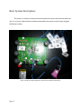
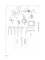
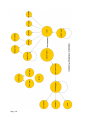
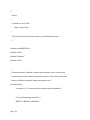
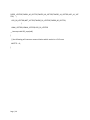
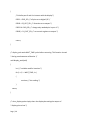
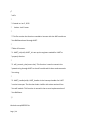
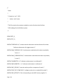
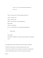
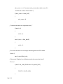
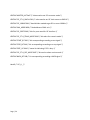
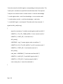
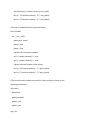
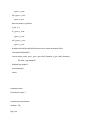
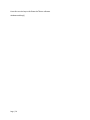
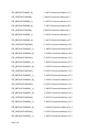
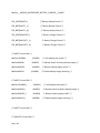
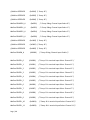
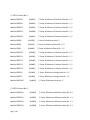
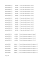
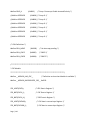
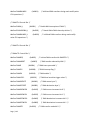
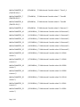
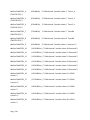
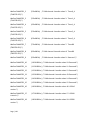
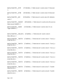
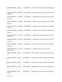
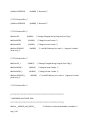
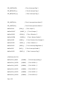
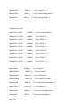
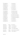
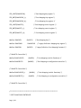
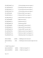
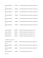
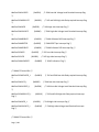
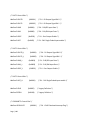
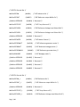
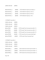
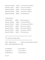
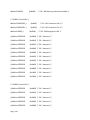
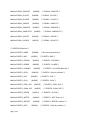
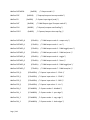
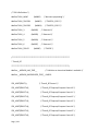
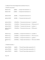
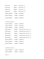
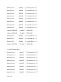
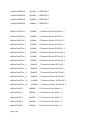
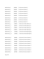
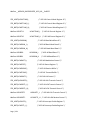
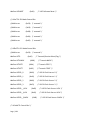
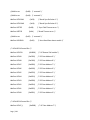
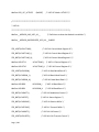
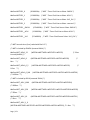
Figure 1: Birds-eye image of BioSleeve system with numbered components
Page | 3
User Manual:
Each of the numbered components in figure 1 are needed for the user to properly
interact with BioSleeve system and will be addressed individually.
1. The four LEDs labeled 1 indicate the status of the system’s wifi module. The user can
determine if a connection has been properly established by checking that the third LED
from the left is on (not blinking). The fourth LED from the left blinks whenever a data
transfer occurs via the wifi module. This allows the user to easily check to see if data is
being transmitted. The first two LEDs are less useful for normal use of the system.
2. The component labeled 2 is the system’s electrode array. For proper use, the user
should peel the electrodes off of the attached plastic and stick them to the user’s arm. It
should be noted that it is not necessary to use the electrode array when playing Ball
Blasters Infinity.
3. The component labeled 3 is the system’s wifi module. The user only needs to know that
it is important to keep loose wires or other conductive material away from the module
as it will interfere with data transmission.
4. The component labeled 4 is the system’s LED display. The display serves two distinct
purposes. The first is displaying the loading time of a calibration sequence. When a
calibration sequence is initiated, the LED display will clear and display a loading bar
sequence over the next few seconds. During this time, the user should not move the
accelerometer glove or calibration will be unsuccessful. When the system is not
calibrating, the LED display samples the data read from the electrodes and displays a
magnitude form of it. This allows the user to see how much muscle action is being
measured through the electrode array (component 2).
5. The components labeled 5 are the system’s charging jacks. The left charging jack accepts
a standard barrel jack. When using a barrel jack, the system will be able to both charge
the battery and run off the jack power. The right jack is a USB 3.0 jack. It should be
noted that the USB jack will only charge the battery, it does not supply power to the
system, and therefore it is recommended to use a barrel jack if both options are
available.
6. The component labeled 6 is the system’s charging LED. It quite simply turns on when the
battery is charging. If the system is plugged in and the LED is not on, then the battery is
fully charged.
7. Component 7 is the system’s power switch.
8. Component 8 is the system’s calibration and reset button. When playing Ball Blasters
Infinity, the user may find that the accelerometer glove is not properly centered. If this
Page | 4
is the case, the user can press component 8 to trigger a recalibration sequence. During
this period, which is displayed on the LED display, the user should hold the
accelerometer glove in the position that the user desires to be the zero position (when
the glove is in the zero position, the blue ball in Ball Blasters Infinity will not move). If
the system experiences an unknown error, the user is recommended to press the
recalibration button as it also resets the CPU.
9. Component 9 is the system’s rechargeable battery. Should the battery ever wear out, it
can be easily replaced by the user by simply plugging a new battery to the onboard jack.
10. Component 10 is the system’s accelerometer glove. The glove is used to control the
blue ball in Ball Blasters Infinity. It is recommended that the user put the glove on
his/her index finger with the blue wires facing upwards when the user’s finger is parallel
to the ground. When this is done, tilting the user’s finger upwards will cause the blue
ball to move up, tilting downwards will cause the blue ball to move down, tilting left will
move the blue ball left, and tilting right will move the blue ball right. It should also be
noted that any combination of two directions will cause diagonal movement. If
directional movement is not satisfactory, a recalibration is recommended.
11. Component 11 is a jumper which determines whether the wifi module is in adhoc or
standard mode. If the wifi module has been configured for the user’s wireless network,
standard mode is highly recommended, and the jumper should be taken out. However,
if the wifi module has not been configured, it must be set to adhoc mode by putting the
jumper into place. In adhoc mode, the wifi module will create its own network which
must be connected to by the computer that the user wishes to play Ball Blasters Infinity
on.
To play Ball Blasters Infinity, the user should first optionally attach the electrode array to his or
her arm. Next the user is recommended to put on the accelerometer glove and hold his/her
finger in the desired zero position. Next the user should turn the system on via the power
switch. The display will then enter calibration mode and begin displaying a loading bar. During
this period the user should not move his/her finger. Once the loading bar has cleared the user
should boot up Ball Blasters Infinity by double clicking on the desktop icon. This will cause the
game to be loaded. It should be noted that the computer running Ball Blasters Infinity must be
on the same wireless network as the wifi module on the board or the computer must be
connected to the adhoc network generated by the wifi module depending on the whether the
jumper (component 11) is in place or not.
Once loaded, Ball Blasters Infinity is quite simple to play. The game will start with a blue ball in
the center of the playing environment. This is the user’s ball and can be controlled by tilting the
Page | 5
accelerometer glove. Every few seconds a red ball and green ball will simultaneously enter the
playing environment. The goal of Ball Blasters Infinity is for the user ball to collide with as many
green balls as possible before colliding with a red ball. Each collision with a green ball will
increment the score count in the top left of the play environment. When the user’s blue ball
collides with a red ball, all red and green balls on the field disappear and the score resets. It
should be noted that the user cannot move the blue ball beyond the bounds of the playing
environment and that red and green balls will bounce off of the boundaries. If the user initiates
a recalibration sequence while playing Ball Blasters Infinity, the game will pause until the
calibration finishes. Also, if the wifi connection is temporarily interrupted, the game will pause
until data is being properly transferred again.
Page | 6
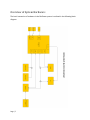
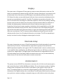
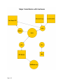
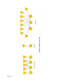
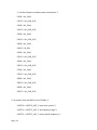
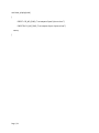
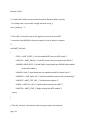
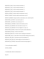
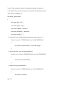
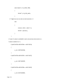
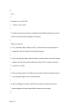
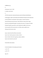
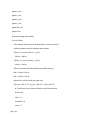
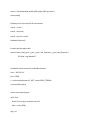
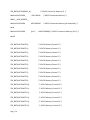
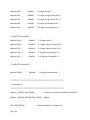
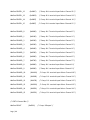
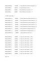
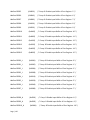
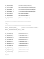
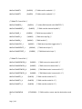
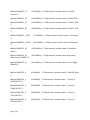
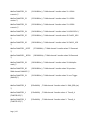
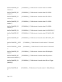
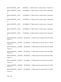
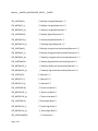
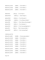
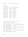
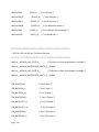
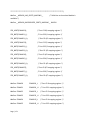
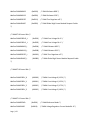
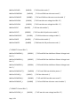
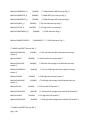
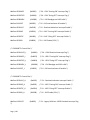
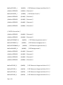
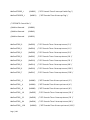
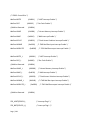
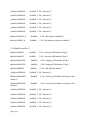
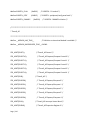
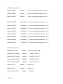
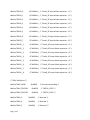
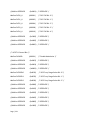
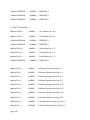
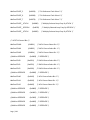
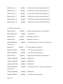
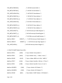
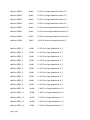
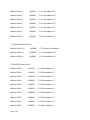
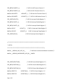
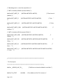
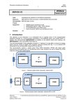
Overview of System Hardware:
The basic interaction of hardware in the BioSleeve system is outlined in the following block
diagram.
Page | 7
Explanation of Each Block:
CPU: The system uses an MSP430F5335 processor. The CPU is the core of the system; all other
block interacts directly with the CPU. The CPU is designed to interact with peripherals through
separate ports which can be configured to have a wide range of functions. Ports are either
configured as non-distinct I/O or to specific functions, such as ADC and UART. It should be
noted that this CPU contains internal flash memory and SRAM, so external memory is not
needed.
JTAG: The JTAG block allows debuggers to interface with the CPU.
Clock Logic: The clock logic block is used to source a 32 KHz external clock which can then be
internally multiplied to generate the master clock of the system.
Reset Logic: Reset logic allows the user to reset the system and trigger calibration sequences on
demand.
Display: The display block is used to convey information to the user.
IMU: although unused in the current implementation of the BioSleeve, the IMU can be used to
determine angular offset of the system.
Electrode Array: The electrode array measures electrical activity in the user’s arm, which is
converted to a digital signal in the CPU then sent to the display.
Accelerometer: The accelerometer is used to detect position changes in the accelerometer
glove which is used to control the Ball Blasters Infinity game.
Wifi Module: The wifi module is used to send and receive data to /from the client running Ball
Blasters Infinity.
Ball Blasters Infinity Client: This block runs the game and receives data from the BioSleeve
board.
Page | 8
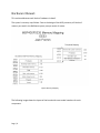
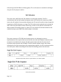
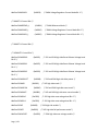
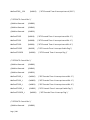
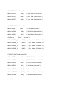
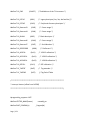
Hardware Manual:
This section addresses each block of hardware in detail.
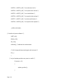
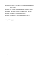
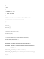
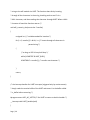
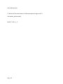
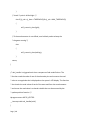
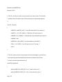
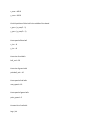
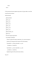
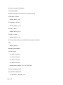
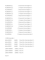
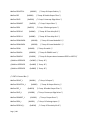
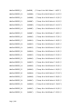
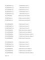
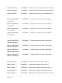
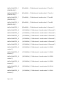
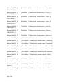
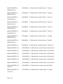
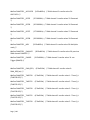
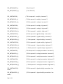
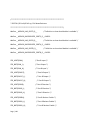
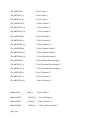
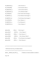
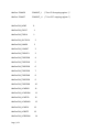
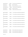
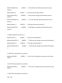
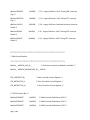
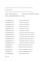
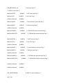
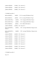
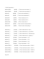
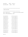
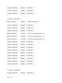
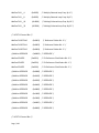
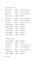
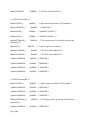
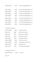
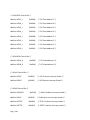
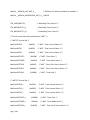
The system’s memory map follows. Due to the design of the MSP processor, all blocks of
memory are used in the BioSleeve system, except vacant of course.
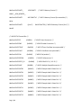
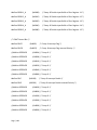
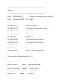
System Memory Mapping
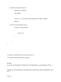
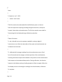
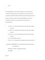
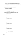
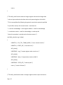
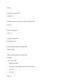
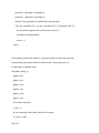
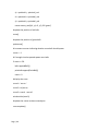
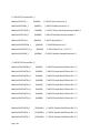
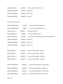
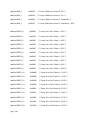
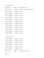
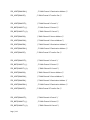
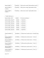
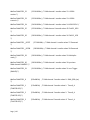
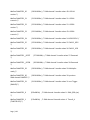
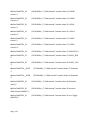
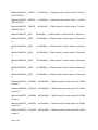
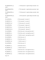
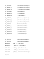
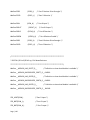
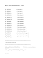
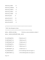
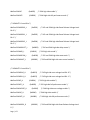
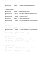
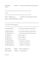
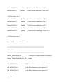
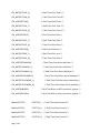
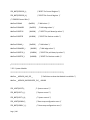
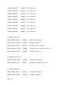
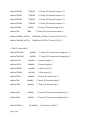
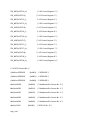
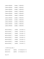
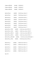
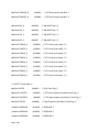
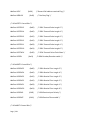
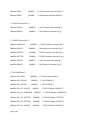
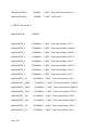
The following image shows the layout of the board with exact model numbers for each
component.
Page | 9
Page | 10
CPU, Clock Logic, Reset Logic, and Power:
This subsection covers the interactions of the CPU, clock logic, reset logic, and power setup
used in the BioSleeve system.
CPU:
The system uses an MSP430F5335 CPU. The CPU is designed to have many multifunctional,
separate ports which interact with peripherals. The CPU of the system has its JTAG pins
extended to a header which allows a JTAG debugger to connect to the CPU.
Clock Logic:
The system’s clock logic is handled primarily inside the CPU, which uses an adjustable PLL to
control the system’s clock frequency. The system uses an external 32 kilohertz crystal as
reference for the PLL, which can be seen on the board layout. The internal PLL of the system is
set up via code to generate a 2.15 megahertz master clock.
Reset Logic:
The system uses a MAX809S chip and normally closed single pole single throw switch to handle
resets. When the MAX809S detects a drop in voltage passed a preset threshold (2.93 V), it sets
the reset signal low (active). This means that the system will be held in reset if the battery runs
too low. The VCC pin of the MAX809S is connected to a normally closed switch which is
connected to VCC. The pin is also connected to a large resistor to ground. When the switch is
pressed, the connection to VCC is lost and the voltage of the reset chip drops enough to trigger
the reset signal, which is connected to the nRST pin on the CPU. Releasing the switch returns
voltage to the reset chips pin and causes the reset signal to go inactive.
Power:
The system uses a barrel jack, USB3.0 jack, LP-063450 lithium ion rechargeable battery,
MAX1555 battery management chip, and a MAX1927R switching regulator to establish a system
voltage of 3.3 Volts. The power from either or both of the two power jacks is fed into MAX1555
which monitors the voltage of the rechargeable battery and sets the voltage on the BAT pin to
maximize the batteries charging. The BAT pin is directly connected to both the positive terminal
of the battery and the input of the MAX1927R switching regulator. This allows the switching
regulator to get power from either the MAX1555 when a power jack is plugged in, or the
battery when no jack is plugged in. The switching regulator converts the input voltage to an
output voltage of 3.3 Volts, which is supplied to the rest of the system. The MAX1927R can
source a total of 800mA; the system uses around 600 mA at maximum capacity.
Page | 11
Display:
The system uses a 10 segment LED bar graph as a way to convey information to the user. The
display is connected to the board through a 470 Ohm resistor network that is connected to a 14
pin dip socket. Each of the bars on the LED display is controlled by a different I/O pin of the
CPU. Eight of the bars are controlled by port 9 (all port 9 pins are used on the display) and the
last two are controlled by the pins P4.3 and P4.4. The display has two distinct functions. The
first is to show the time remaining for a calibration sequence. It does this by showing a loading
bar that moves across the display over the course of several seconds. When the calibration is
finished, the display pauses momentarily with all bars lit before returning to its normal
functioning. During normal system operation, the display is fed a magnitude form of the data
read from the electrode array by the CPU. Due to the refresh rate on the display being quite
high and the electrodes having extreme variation in signal, the displaying of electrode signals is
often not very luminous. The CPU interacts with the display by setting all of port 9 and the
relevant portion of port 4 to I/O mode with direction set to output. The LED corresponding to
each pin can then be set by changing the output signal on the pin.
Electrode Array:
The system incorporates an array of 9 EasyTrode brand silver chloride electrodes for measuring
muscle activity of the user. The electrodes are separated into groups of two and fed into
INA331 operational amplifiers with a gain of 100. The odd electrode is used as a reference and
is not amplified. After amplification, the differential signal is fed to an ADC12 pin on the CPU for
conversion to a digital signal. The digital signal is then converted to a magnitude form by the
CPU before being sent to the display. When connected to the user’s arm, the electrode array
allows the user to see electrical activity due to muscle contractions.
Accelerometer:
The system uses an ADXL335 accelerometer to measure the tilt of the accelerometer glove
and control the player’s ball in Ball Blasters Infinity. The accelerometer produces 3 analog
voltages that correspond to the tilt of the accelerometer (one signal for each of the 3D
axes). The analog signals are converted to digital signals by ADC12 pins. The CPU then
determines if the signals indicate the accelerometer is sufficiently tilted from the calculated
zero position to warrant sending a command string over wifi (which results in the player
Page | 12
ball moving in the Ball Blasters Infinity game). The accelerometer is attached to the finger
of a glove for the players comfort.
Wifi Module:
The system uses a WiFly RN-131C wifi module to transfer data wirelessly. The CPU
communicates with the wifi module through two wire UART interface at a baud rate of 9600
(set by the wifi module). Communication between the CPU and wifi module is done through the
transmission of ASCII characters or strings. The CPU is able to both send and receive strings via
UART. When the wifi module receives a full string, it sends it to any devices connected to its
adhoc network (if the adhoc jumper is in place) or to any devices on the same network as the
module listening to port 2000 (if the adhoc jumper is removed).
IMU:
The system contains an ITG-3200 inertial measurement unit. Although the current
implementation of the system does not use the IMU, the code and hardware needed for IMU
interaction is included in this manual. The IMU communicates with the CPU over the I2C
interface at a data transfer rate of 100Khz. The IMU contains registers which store values
indicating the tilt of the internal gyros. By accessing these registers, the CPU can determine the
tilt of the system. When interacting with the IMU, the following protocol must be used.
Read Protocol for IMU, with RA = register address, AD = address of IMU
Write protocol for IMU
Page | 13
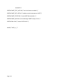
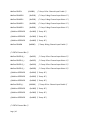
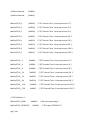
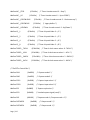
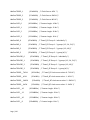
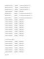
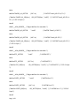
Software Manual:
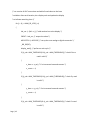
This section details how the software run by the system works.
The following image is a diagram of how each of the functions of the software interacts with
each other and the hardware.
For more detailed explanations on how the software works, see the software section at the end
of this manual.
Page | 14
Page | 15
Explanation of Files:
main.c:
main.c is the code that is run immediately after a system reset or power up. main.c immediately
sets up all ports of the CPU to minimize power consumption and then moves on to set up the
universal clock system to generate a master clock of 2.15 megahertz. Main.c then calls all the
initialization functions needed for the system to interact with the hardware. Once fully
initialized, the code enters the main loop, which performs analog to digital conversions and
checks whether command characters need to be sent to the wifi module. This loop continues
indefinitely.
display.c:
display.c contains the functions needed to initialize the pins used to control the display and
clear the display when necessary. This is accomplished through direct output control of the pins
used to interact with the display.
adc.c:
adc.c is the code used to regulate all analog to digital conversions in the system. adc.c controls
the CPU’s interaction with both the electrode array and accelerometer. The code contains the
basic adc initialization code as well as the calibration code needed to calculate a zero point for
the accelerometer. The code also sets up an interrupt that is generated each time an adc
conversion cycle finish. One adc conversion cycle is set to make many adc readings (one for
each pin of ADC12 used). When an adc interrupt occurs, the adc handler reads from the
electrode array, converts the read data to a magnitude, and displays one of the converted
values on the display. The electrode displayed is determined by a shared counter variable that
iterates through the number of electrodes before resetting. The handler also stores the
accelerometer values read in a shared variable that is used by the update position function to
determine if the accelerometer is sufficiently shifted to warrant the transmission of a command
string.
Page | 16
wifi.c:
wifi.c contains the code used to initialize and run the UART controller of the system. The code is
used to establish the appropriate baud rate to interact with the wifi module and also contains
the code needed to send strings via wifi. The code also includes UART receive interrupts. The
interrupt handler stores the received character in a buffer that is not used in the current system
implementation.
I2C.c:
I2C.c contains the code needed to initialize the I2C controller of the system, send data to any of
the registers of the system’s IMU and read data from any of the registers of the system’s IMU.
This code is not used in the system’s current implementation.
BallBlasters.py:
BallBlasters.py controls the flow of wireless data on the client computer and controls the game
environment of Ball Blasters Infinity. When BallBlasters.py is run, it first connects to the wifi
module on the BIoSleeve system, note that it can only do this if the host computer is either
connected to the adhoc network generated by the wifi module, or on the same wireless
network as the wifi module. The program then creates a TkInter graphical environment that is
used to play the game in. Each time data is received via wifi, the game updates the graphical
interface and occasionally adds balls. Balls are generated with a random velocity that
determines how much each update changes their position, causing them to appear to move.
Each update, the program checks if the players blue ball has collided with any of the other balls
and reacts accordingly. Whenever a command string is received, the game updates the position
of the players blue ball.
Page | 17
Page | 18
Page | 19
Explanation of Function Diagrams:
The system is initialized during the non-loop portion of main.c. In the initialization code, the
master clock is established, all ports are set to use minimal power, and the peripheral
initialization code is called. main.c then proceeds to enter the main loop and run the system by
continually reactivating adc reads and occasionally checking if a command string should be
sent. Each time an adc read finishes, an adc interrupt triggers the adc_handler function, which
displays the magnitude of electrical activity being measured in the electrode array and updates
the shared variables indicating what position the accelerometer is in. When update_position is
called it checks if the accelerometer is shifted sufficiently from its zero position to warrant the
transfer of a command character. If a command character should be sent, wifi_transmit_char is
passed the appropriate command string which is then sent out over UART to the wifi module
before being transmitted to the client running Ball Blasters Infinity for processing. If a character
is ever received by the wifi module, it triggers UART_handler, which stores the character in
in_buffer for potential further handling.
Page | 20
System Code:
Note that code is written in c except for BallBlasters.py which is written in python. C files are of
type .c, c headers are of type .h, and python files of type .py. Also note that it is almost certainly
easier to view the following files directly in the attached .zip containing all system code.
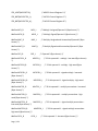
Table of Contents:
1. main.c
2. display.h
3. display.c
4. wifi.h
5. wifi.c
6. adc.h
7. adc.c
8. I2C.h
9. I2C.c
10. BallBlasters.py
11. msp430f5335.h
Page | 21
/*
* main.c
*
* Created on: Jun 4, 2012
*
Author: Josh Fromm
*
* This file contains the main loop used to run the BioSleeve system.
*/
#include <msp430f5335.h>
#include "wifi.h"
#include "display.h"
#include "adc.h"
/* the main function initializes all major system registers, the universal clock
* system and runs all the coded initialization functions. The main function then
* enters an infinite loop which allows the system to run */
void main(void) {
int counter = 0; /* counter used to space out position updates */
/* turn off watch dog controller */
WDTCTL = WDTPW + WDTHOLD;
Page | 22
/* initialize all ports to reduce power consumption */
P1DIR = ALL_PINS;
P1OUT = ALL_PINS_OUT;
P2DIR = ALL_PINS;
P2OUT = ALL_PINS_OUT;
P3DIR = ALL_PINS;
P3OUT = ALL_PINS_OUT;
P4DIR = ALL_PINS;
P4OUT = P4_DIR;
P5DIR = ALL_PINS;
P5OUT = ALL_PINS_OUT;
P6DIR = ALL_PINS;
P6OUT = ALL_PINS_OUT;
P7DIR = ALL_PINS;
P7OUT = ALL_PINS_OUT;
P8DIR = ALL_PINS;
P8OUT = ALL_PINS_OUT;
P9DIR = ALL_PINS;
P9OUT = ALL_PINS_OUT;
/* set master clock and SMCLK to be 2.15Mhz */
UCSCTL0 = UCSCTL0_INIT; /* reset clock system */
UCSCTL1 = UCSCTL1_INIT; /* set frequency range */
UCSCTL2 = UCSCTL2_INIT; /* select specific frequency */
Page | 23
UCSCTL3 = UCSCTL3_INIT; /* set reference clock */
UCSCTL4 = UCSCTL4_INIT; /* set system clock sources */
UCSCTL5 = UCSCTL5_INIT; /* set clock dividers */
UCSCTL6 = UCSCTL6_INIT; /* set special clock settings */
UCSCTL7 = UCSCTL7_INIT; /* set fault notifications */
UCSCTL8 = UCSCTL8_INIT; /* set special clock requests */
_enable_interrupt();
/* initialize all system software */
UART_init();
display_init();
adc_init();
calibrate(); /* calibrate the accelerometer
/* chill in loop and keep resetting the adc interrupts */
for (;;)
{
/* only call update position every once in a while */
if (counter == 0)
{
update_position();
}
Page | 24
/* prepare for another adc cycle */
ADC12CTL0 |= ADC12SC;
_BIS_SR(GIE);
counter += 1; /* increment counter keeping track of when to update
* position */
/* check if counter should be reset */
if (counter == MAX_COUNT)
{
counter = 0;
}
}
}
/* Initialize non-used ISR vectors with a trap function */
/* currently all interrupt vectors are unused */
#pragma
vector=RTC_VECTOR,PORT2_VECTOR,PORT1_VECTOR,TIMER1_A1_VECTOR,DMA_VECTOR, \
TIMER0_A1_VECTOR,TIMER0_A0_VECTOR,COMP_B_VECTOR,LDO_PWR_VECTOR,PORT3_VECT
OR, \
Page | 25
PORT4_VECTOR,TIMER1_A0_VECTOR,TIMER2_A0_VECTOR,TIMER2_A1_VECTOR,USCI_A1_VEC
TOR, \
USCI_B0_VECTOR,WDT_VECTOR,TIMER0_B1_VECTOR,TIMER0_B0_VECTOR,
\
UNMI_VECTOR,SYSNMI_VECTOR,USCI_B1_VECTOR
__interrupt void ISR_trap(void)
{
// the following will cause an access violation which results in a PUC reset
WDTCTL = 0;
}
Page | 26
/*
* display.h
*
* Created on: Jun 4, 2012
*
Author: Josh Fromm
*
* This file contains the constants used to initialze the LED display for the
* BioSleeve system.
*/
#ifndef DISPLAY_H_
#define DISPLAY_H_
/* initialize pins used to interact with display */
void display_init(void);
/* wait for a while */
void display_wait(void);
/* turn off all LEDs on the display */
void clear_display(void);
#DEFINE P9IO_SEL 0x0 /* value used to select I/O for all pins of port 9 */
#DEFINE P9_OUT_SEL 0xFF /* value used to set all port 9 pins to output */
Page | 27
#DEFINE P4IO_SEL 0xFFE9 /* value used to set bits corresponding to needed port
4 pins to I/O */
#DEFINE P4_OUT_SEL 0x16 /* value used to set needed port 4 pins to output */
#DEFINE WAIT_TIME 0xF000 /* number of cycles before display_wait ends */
#DEFINE P9_NO_PINS 0x0 /* clear all display pins in port 9 */
#DEFINE P4_NO_PINS 0xFFE7 /* use to clear all display pins in port 4 */
#endif /* DISPLAY_H_ */
Page | 28
/*
* display.c
*
* Created on: Jun 4, 2012
*
Author: Josh Fromm
*
* This file contains the function used to initialize the bar panel LED display
* used in the BioSleeve system.
*
* Table of Contents:
* 1. display_init(void): display_init sets up the registers needed for the CPU
* to interact with the system's LED display.
* 2. display_wait(void): display_wait holds for a set amount of time and is
* used for calibration.
* 3. clear_display(void): clears the display */
*/
#include "display.h"
#include <msp430f5335.h>
/* display_init takes no inputs and has no outputs. The function sets up the
* the ports needed to interact with the display by appropriately selecting
* their function and direction. */
void display_init(void)
Page | 29
{
/*initialize port 9 and 4 to interact with the display*/
P9SEL = P9IO_SEL; /* all pins set to digital I/O */
P9DIR = P9_OUT_SEL; /* direction set to output */
P4SEL &= P4IO_SEL; /* change only needed pins in port 4 */
P4DIR |= P4_OUT_SEL; /* set control registers to output */
return;
}
/* display_wait waits WAIT_TIME cycles before returning. This function is used
* during accelerometer calibration */
void display_wait(void)
{
int i; /* variable used for iteration */
for (i = 0; i < WAIT_TIME; i++)
{
continue; /* do nothing */
}
return;
}
/* clear_display quite simply clears the display be setting the output of
* display pins to low */
Page | 30
void clear_display(void)
{
P9OUT = P9_NO_PINS; /* set output of port 9 pins to low */
P4OUT &= P4_NO_PINS; /* set output of port 4 pins to low */
return;
}
Page | 31
/*
* wifi.h
*
* Created on: Jun 6, 2012
*
Author: Josh Fromm
*
* This file contains the constants needed to establish a UART connection
* to the wifi module and transmit characters via wifi.
*/
#ifndef WIFI_H_
#define WIFI_H_
/* Initialize the UART module on CPU */
void UART_init(void);
/* Transmit the passed string to the wifi module for transmission */
void wifi_transmit_char(const char *);
#DEFINE UART_PORTS 0x30 /* value to set UART ports to UART mode */
#DEFINE BAUD_RATE 0xD0 /* divisor giving a baud rate of 9600 from a clock source
of 2.15 MHz */
#DEFINE UART_SMCLK 0xC0 /* sets UART to use SMCLK */
#DEFINE UART_MOD_SEL 0x44 /* sets a modulation pattern and leaves oversampling
Page | 32
turned off */
#DEFINE UART_STAT_INIT 0x0 /* sets initial status variables */
#DEFINE UART_REC_INT 0x1 /* enables receive interrupts on UART */
#DEFINE UART_START 0x0 /* starts UART data transfers */
#DEFINE UART_BUSY 0x1 /* bit indicating if UART is busy or free */
#DEFINE NULL 0x0 /* value of ASCII NULL */
#endif /* WIFI_H_ */
Page | 33
/*
* wifi.c
*
* Created on: Jun 5, 2012
*
Author: Josh Fromm
*
* This file contains the functions needed to interact with the Wifi module on
* the BioSleeve board through UART.
*
* Table of Contents:
* 1. UART_init(void): UART_init sets up the registers needed for UART to
* properly function.
*
* 2. wifi_transmit_char(const char): This function is used to transmit the
* passed string through UART to the wifi module which then sends transmits
* the string.
*
* 3. UART_handler(void): UART_handler is the interrupt handler for UART
* receive interrupts. The function loads a buffer with value received from
* the wifi module. This function is unused in the current implementation of
* the BioSleeve.
*/
#include <msp430f5335.h>
Page | 34
#include "wifi.h"
/* Create buffer used to store received characters. Because buffer currently
* isn't being used, it can contain a single character string. */
char in_buffer[] = '?';
/* The UART_init function sets up the registers necesarry for the UART
* controller of the MSP430 to function properly. It has no inputs or outputs.
*/
void UART_init(void)
{
P2SEL |= UART_PORTS; /* set the needed UART ports to UART mode */
UCA0CTL1 = UART_SMCLK; /* set UART source clock to be equal to the MCLK */
UCA0BR0 = BAUD_RATE; /* divide SMCLK to give baud rate of 9600 (value needed
by the wifi module */
UCA0BR1 = 0x0; /* upper baud rate not needed since MCLK relatively low */
UCA0MCTL = UART_MOD_SEL; /* pick bit modulation and turn off oversampling */
UCA0STAT = UART_STAT_INIT; /* initialize status register */
UCA0IE = UART_REC_INT; /* enable receive interrupts on UART */
UCA0CTL0 = UART_START; /* Begin running the UART module */
return;
}
/* The wifi_transmit_char function takes a string as input and sends that
Page | 35
* string to the wifi module via UART. The function does this by iterating
* through all the characters in the string, checking each to see if it is a
* NULL character, and then sending that character through UART. When a NULL
* character is found the function returns */
void wifi_transmit_char(const char *transfer)
{
unsigned int i; /* variable needed for iteration */
for (i = 0; transfer[i] != NULL; i++) /* iterate through all characters in
passed string */
{
/* as long as USCI is busy hold loop */
while (UCA0STAT & UART_BUSY);
UCA0TXBUF = transfer[i]; /* transfer next character */
}
return;
}
/* the interrupt handler for UART interrupts (triggered only by receive events)
* simply reads the receive buffer of the UART and stores it in the buffer called
* in_buffer before returning */
#pragma vector=USCI_A0_VECTOR /* Set UART int vector to be this handler */
__interrupt void UART_handler(void)
{
Page | 36
in_buffer = UCA0RXBUF; /* read receive buffer */
return;
}
Page | 37
/*
* adc.h
*
* Created on: Jun 7, 2012
*
Author: Josh Fromm
*
* This file contains the constants needed to run the functions that facilitate
* ADC readings for the BioSleeve system.
*/
#ifndef ADC_H_
#define ADC_H_
#DEFINE THRESHOLD 4 /* constant used to determine minimum distance from base
* before accelerometer tilt triggers output */
#DEFINE MIN_THRESHOLD 20 /* accelerometer reads below this value are probably
* errors */
#DEFINE MAX_THRESHOLD 240 /* accelerometer reads above this value are probably
* errors */
#DEFINE CALIBRATED = 0 /* indicates accelerometer is uncalibrated */
#DEFINE UNCALIBRATED = 1 /* indicates accelerometer is calibrated */
#DEFINE ADC_SEQ 0X2 /* sets adc reads to perform a sequence of reads */
#DEFINE EIGHT_BIT_STAND 0X0 /* configures adc to be in standard 8 bit mode */
#DEFINE ADC_BITS 0X7F /* bits corresponding to used ADC memory registers */
Page | 38
#DEFINE ELEC_0 0X0 /* adc port used for electrode 0 */
#DEFINE ELEC_1 0X1 /* adc port used for electrode 1 */
#DEFINE ELEC_2 0X2 /* adc port used for electrode 2 */
#DEFINE ELEC_3 0X3 /* adc port used for electrode 3 */
#DEFINE X_AXIS 0X5 /* adc port used for accelerometer x axis */
#DEFINE Y_AXIS 0X7 /* adc port used for accelerometer y axis */
#DEFINE Z_AXIS 0X8E /* adc port used for accelerometer z axis + end of seq bit */
#DEFINE PORT_6_ADC 0XFF /* pins used on port 6 */
#DEFINE PORT_7_ADC 0XF0 /* pins used on port 7 */
#DEFINE NUM_P9_LEDS 0X8 /* number of leds used on port 9 */
#DEFINE P4_LED_LOW 0X8 /* bit for the lower bar on port 4 */
#DEFINE P4_LED_HIGH 0X10 /* bit for the higher bar on port 4 */
#DEFINE PAUSE_DUR 0X4 /* number of wait cycles at end of calibration */
#DEFINE NUM_ELEC 0X4 /* number of electrodes */
#DEFINE RAIL_NOISE 255 /* common incorrect reading from electrodes */
#DEFINE CONV_VAL 25 /* value used to convert electrode reading into bar values */
#DEFINE P4_LOW_TRIG 9 /* indicates low port 4 led should be lit */
#DEFINE P4_HIGH_TRIG 10 /* indicates high port 4 led should be lit */
#DEFINE ADC_INT_RST 0X0 /* value used to reset adc interrupt register */
/* sets up adc registers needed */
void adc_init(void);
/* calculates base values for accelerometer */
Page | 39
void calibrate(void);
/* determines if accelerometer is shifted and outputs strings to wifi */
void update_position(void);
#endif /* ADC_H_ */
Page | 40
/*
* adc.c
*
* Created on: Jun 7, 2012
*
Author: Josh Fromm
*
* This file contains the code needed for the BioSleeve system to interact
* with all components requiring an analog to digital conversion, namely the
* system's electrodes and accelerometer. The file also contains some code for
* interacting with the display during a calibration procedure
*
* Table of Contents:
* 1. adc_init(void): sets up the registers needed for analog to digital \
* conversions to run. Both the electrodes of the system and accelerometer are
* initialzed in this function.
*
* 2. calibrate(void): averages readings from the accelerometer over a fixed
* set of time and sets the average as the base position of the accelerometer,
* meaning directional outputs will be based on the position of the accelerometer
* with respect to the calculated base position. During calibration, the function
* outputs to the display causing a loading sequence of bars to appear. When the
* the display returns to showing the readings from the electrodes, calibration
* is complete.
*
Page | 41
* 3. update_position(void): checks the values of the acelerometer and transmits
* directional outputs via UART if the the x or y axes are sufficiently shifted
* from their base positions.
*
* 4. adc_handler(void): handles a read of the adc ports on the CPU. Outputs
* an electrode pattern to the display and updates the values read from the
* accelerometer.
*/
#include <msp430f5335.h>
#include "adc.h"
#include "display.h"
#include "wifi.h"
/* shared variables */
int elec_count = 0; /* counter used to keep track of which electrode should be
output to the display */
int x_val; /* value used for most recent x-axis accelerometer read */
int y_val; /* value used for most recent y-axis acceleromter read */
int z_val; /* value used for most recent z-axis accelerometer read */
int x_base = 0; /* calculated zero position of accelerometer along x-axis */
int y_base = 0; /* calculated zero position of accelerometer along y-axis */
int z_base = 0; /* calculated zero position of accelerometer along z-axis */
int uncalibrated = UNCALIBRATED; /* variable indicating whether a calibration
has occurred */
Page | 42
/* adc_init sets up the registers needed for analog to digital conversions to
* take place. The function takes no inputs and has no outputs */
void adc_init(void)
{
ADC12CTL0 = ADC12SHT02 + ADC12ON + ADC12MSC; /* set a sample and hold time
* of 16 cycles, turn on analog
* to digital conversion and
* set rising edges to trigger
* sampling */
ADC12CTL1 = ADC12SHP + ADC_SEQ; /* use sampling timer for sequence of reads */
ADC12CTL2 = EIGHT_BIT_STAND; /* use 8 bit mode with standard settings */
ADC12IE = ADC_BITS; /* enable electrode and accelerometer interrupts */
ADC12MCTL0 = ELEC_0; /* set first ADC memory register to adc port 0 */
ADC12MCTL1 = ELEC_1; /* set second ADC memory register to adc port 1 */
ADC12MCTL2 = ELEC_2; /* set third ADC memory register to adc port 2 */
ADC12MCTL3 = ELEC_3; /* set fourth ADC memory register to adc port 3 */
ADC12MCTL4 = X_AXIS; /* set fifth ADC memory register to adc port 5 */
ADC12MCTL5 = Y_AXIS; /* set sixth ADC memory register to adc port 7 */
ADC12MCTL6 = Z_AXIS; /* indicate seventh ADC memory register is last of sequence
and set it to read from adc port 15 */
ADC12CTL0 |= ADC12ENC; /* enable ADC */
P6SEL |= PORT_6_ADC; /* set port 6 entirely to ADC mode */
P7SEL |= PORT_7_ADC; /* set adc pins of port 7 to ADC mode */
Page | 43
return;
}
/* The calibrate function uses a series of readings from the accelerometer to
* compute an average position. This average position is then stored for future
* comparisons to determime offsets from the base position. During the calibration
* process, this function outputs an incrementing loading bar to the system's
* LED display. calibrate has no inputs and does not return anything. */
void calibrate(void)
{
int x_count = 0; /* counter used to determine how many valid x readings
occured */
int y_count = 0;/* counter used to determine how many valid y readings
occured */
int z_count = 0;/* counter used to determine how many valid z readings
occured */
int j; /* variable used for iteration */
int led_var = 0; /* variable used for changing output of display iteratively */
uncalibrated = UNCALIBRATED; /* set uncalibrated variable to indicate system
is not calibrated */
ADC12CTL0 |= ADC12SC; /* trigger an ADC read */
_BIS_SR(GIE);
Page | 44
/* run a series of ADC conversions and add all read values to the base
* variables. after each iteration, do a display wait and update the display
* to indicate remaining time */
for (j = 0; j < NUM_P9_LEDS; j++)
{
led_var |= (0x1 << j); /* add another bar to the display */
P9OUT = led_var; /* output the value */
ADC12CTL0 |= ADC12SC; /* set up the next analog to digital conversion */
_BIS_SR(GIE);
display_wait(); /* perform a wait cycle */
if ((x_val > MIN_THRESHOLD) & (x_val < MAX_THRESHOLD)) /* check if the x
read is valid */
{
x_base += x_val; /* if so increment base and counter */
x_count += 1;
}
if ((y_val > MIN_THRESHOLD) & (y_val < MAX_THRESHOLD)) /* check if y read
is valid */
{
y_base += y_val; /* if so increment base and counter */
y_count += 1;
}
if ((z_val > MIN_THRESHOLD) & (z_val < MAX_THRESHOLD)) /* check if z read
is valid */
Page | 45
{
z_base += z_val; /* if so increment base and counter */
z_count += 1;
}
}
z_base = z_base/z_count; /* take the average of the bases */
y_base = y_base/y_count;
x_base = x_base/x_count;
P4OUT |= P4_LED_LOW; /* finish loading display */
display_wait();
P4OUT |= P4_LED_HIGH;
for (j = 0; j < PAUSE_DUR; j++) /* pause before clearing display */
{
display_wait();
}
clear_display()
uncalibrated = CALIBRATED; /* indicate that the accelerometer is calibrated */
return;
}
/* the update_position function determines if the accelerometer is sufficiently
* shifted from its base position to warrant sending a character via wifi.
* The function accomplishes this by comparing the reading from the accelerometer
* with the calculated base position for the axis in question plus a threshold
Page | 46
* value. If the read value is above or below the thresholds, a character is
* sent. Because the system currently uses a two dimensional implementation,
* the z axis is not updated. */
void update_position(void)
{
const char left[] = "left ";
const char right[] = "right ";
const char forward[] = "forward ";
const char backward[] = "backward ";
const char nothing[] = " ";
/* check if the x axis is shifted forward enough to send a character */
if ((x_val < (x_base - THRESHOLD)) & (x_val > MIN_THRESHOLD))
{
wifi_transmit_char(forward); /* if so send a string */
}
/* then check if the x axis is shifted backwards */
else if ((x_val > (x_base + THRESHOLD)) & (x_val < MAX_THRESHOLD))
{
wifi_transmit_char(backward);
}
/* check if the y axis is shifted left */
if ((y_val < (y_base - THRESHOLD)) & (y_val > MIN_THRESHOLD))
{
wifi_transmit_char(left);
Page | 47
}
/* check if y axis is shifted right */
else if ((y_val > (y_base + THRESHOLD)) & (y_val < MAX_THRESHOLD))
{
wifi_transmit_char(right);
}
/* if the accelerometer is not shifted, send a blank packet to keep the
* the game running */
else
{
wifi_transmit_char(nothing);
}
return;
}
/* adc_handler is triggered each time a sequence of adc reads finshes. The
* function reads the value of one of the electrode pins and converts the read
* value to a magnitude that is displayed on the system's LED display. The function
* also checks the read values of each of the axes read from the accelerometer
* and stores the read value in a shared variable that can be accessed by the
* update position function */
#pragma vector=ADC12_VECTOR
__interrupt void adc_handler(void)
{
Page | 48
int elec1; /* variable containing the selected electrode reading */
int elec2; /* variable containing the magnitude conversion of elec1 */
int elecout; /* value that is output to the display */
/* only process electrodes if the system is calibrated */
if (uncalibrated == CALIBRATED)
{
clear_display(); /* clear the display */
/* read from one of the electrodes depending on elec_count */
if ( elec_count == 0)
{
elec1 = ADC12MEM0;
}
else if ( elec_count == 1)
{
elec1 = ADC12MEM1;
}
else if ( elec_count == 2)
{
elec1 = ADC12MEM2;
}
else if ( elec_count == 3)
{
elec1 = ADC12MEM3;
}
Page | 49
elec_count += 1; /* increment elec_count and set back to zero if it
exceeds the number of electrodes */
if (elec_count >= NUM_ELEC)
{
elec_count = 0;
}
/* convert read value to a magnitude form */
if (elec1 < 0)
{
elec1 = 0;
}
else if ( elec1 == RAIL_NOISE)
{
elec1 = 0;
}
/* turn the read value into an integer indicating which bar LEDs should
* be set */
elec2 = elec1/CONV_VAL;
/* determine if highest bars of display need to be set and set them if
* if so. */
if (elec2 > P4_LOW_TRIG & elec2 < P4_HIGH_TRIG)
{
P4OUT |= P4_LED_LOW;
}
Page | 50
else if (elec2 >= P4_HIGH_TRIG)
{
P4OUT |= P4_LED_HIGH;
}
/* if high bars not set, then set the lower bars */
else
{
elecout = (0x1 << elec2 - 1);
P9OUT = (elecout);
}
}
/* check if a value is available for each axis and store that value in a
* shared variable if so */
if (ADC12IFG & ADC12IFG4 == ADC12IFG4)
{
x_val = ADC12MEM4;
}
if (ADC12IFG & ADC12IFG5 == ADC12IFG5)
{
y_val = ADC12MEM5;
}
if (ADC12IFG & ADC12IFG6 == ADC12IFG6)
{
z_val = ADC12MEM6;
Page | 51
}
ADC12IFG = ADC_INT_RST; /* reset the interrupt register and return */
return;
}
Page | 52
/*
* I2C.h
*
* Created on: Jun 18, 2012
*
Author: Josh Fromm
*
* This file contains the function declarations and constants needed for the
* the BioSleeve's I2C module to properly interact with the on board IMU.
*/
#ifndef I2C_H_
#define I2C_H_
/* initialize the I2C controller */
void I2C_init(void);
/* wait until I2C bus is ready for further data transfer */
void ACK_check(void);
/* write a value to an IMU register */
void IMU_write(int reg, int data);
/* read a value from an IMU register */
signed int IMU_read(int reg);
Page | 53
#DEFINE MASTER_INIT 0x0F /* Value used to set I2C to master mode */
#DEFINE I2C_CTL1_SMCLK 0X10 /* value used to set I2C clock source to SMCLK */
#DEFINE I2C_100KHZ 0X4 /* baud divider needed to get I2C to run at 100KHz */
#DEFINE IMU_ADDR 0X68 /* fixed address of IMU unit */
#DEFINE I2C_PORTS 0X6 /* bits for ports used for I2C interface */
#DEFINE I2C_CTL1_TRANS_MODE 0X10 /* bit select for transmit mode */
#DEFINE START_BIT 0X2 /* bit corresponding to sending a start signal */
#DEFINE STOP_BIT 0X4 /* bit corresponding to sending to a stop signal */
#DEFINE FREE_I2C 0X10 /* status bit indicating if I2C is busy */
#DEFINE I2C_CTL1_REC_MODE 0XEF /* bit used to select receive mode */
#DEFINE NACK_BIT 0X8 /* bit corresponding to sending a NACK signal */
#endif /* I2C_H_ */
Page | 54
/*
* I2C.c
*
* Created on: Jun 18, 2012
*
Author: Josh Fromm
*
* This file contains the functions needed for the BioSleeve board to interact
* with the on board IMU through I2C interface.
*
* Table of contents:
* 1. I2C_init(void): When called, the I2C_init function sets up the registers
* needed for the I2C interface to function properly.
*
* 2. ACK_check(void): When called, the ACK_check function checks the status
* registers of the I2C module and holds until the I2C is ready for another
* transmit or receive.
*
* 3. IMU_write(reg, data): The IMU_write function writes the passed data to
* to the passed register of the on board IMU.
*
* 4. IMU_read(reg): The IMU_read function reads the data stored in the
* passed register of the on board IMU and returns that value.
*/
Page | 55
#include <msp430f5335.h>
#include "I2C.h"
/* The I2C_init function takes no inputs and has no return value. The function
* initializes the I2C module of the CPU by setting up the associated registers
*/
void I2C_init(void)
{
UCB0CTL0 = MASTER_INIT; /* set to SPI mode with CPU as master */
UCB0CTL1 = I2C_CTL1_SMCLK; /* SMCLK as USCI clock source */
UCB0BR0 = I2C_100KHZ; /* set baud rate to give desired data transfer */
UCB0BR1 = 0x0;
UCB0I2CSA = IMU_ADDR; /* set slave address to the IMU */
P2SEL |= I2C_PORTS; /* set I2C ports to be in I2C mode */
return;
}
/* The ACK_check function simply holds until an acknowledge is received from
* the slave being interacted with and continues to hold until the I2C bus
* is free for further data transmission */
void ACK_check(void)
{
while (UCB0CTL1 & START_BIT != 0); /* wait for first ack */
while (UCB0STAT & FREE_I2C != 0); /* wait until bus is free */
Page | 56
return;
}
/* The IMU_write function takes an integer register value and an integer data
* value as input and writes the data value to the passed register of the IMU.
* This is accomplished by following the general transmission protocol specified
* by the IMU, namely: Set transmit mode -> send start bit
* -> wait for acknowledge -> send register address -> wait for acknowledge
* -> send data to write -> wait for acknowledge -> send stop bit.
* after this procedure is carried out the function returns. */
void IMU_write(int reg, int data)
{
UCB0CTL1 |= I2C_CTL1_TRANS_MODE; /* set to transmit mode */
UCB0CTL1 |= START_BIT; /* send start bit */
ACK_check();
UCB0TXBUF = reg; /* output register value to write to */
ACK_check();
UCB0TXBUF = data; /* output data to write to IMU */
ACK_check();
UCB0TXBUF = STOP_BIT; /* send stop bit */
return; /* write is finished */
}
/* The IMU_read function takes an integer register value as input and returns
Page | 57
* the value stored in the IMU register corresponding to the input number. The
* read cycle is carried out as specified in the IMU data sheet. The required
* steps are: set transmit mode -> send a start bit -> wait for acknowledge
* -> send register value -> wait for acknowledge -> set to receive mode
* -> send another start bit -> wait for acknowledge -> read value
* -> send NACK signal -> send stop bit. The value red is then returned. */
signed int IMU_read(int reg)
{
signed int read_data; /* variable containing data read from IMU */
UCB0CTL1 |= I2C_CTL1_TRANS_MODE; /* set to transmit mode */
UCB0CTL1 |= START_BIT; /* send start bit */
ACK_check();
UCB0TXBUF = reg; /* output register value to read from */
UCB0CTL1 &= I2C_CTL1_REC_MODE; /* set I2C to receive mode */
UCB0CTL1 |= START_BIT; /* send another start bit */
ACK_check();
read_data = UCB0RXBUF; /* load value read from IMU */
UCB0CTL1 |= NACK_BIT; /* send NACK signal to IMU */
UCB0CTL1 |= STOP_BIT; /* send stop signal to IMU */
return read_data; /* return the read value */
}
Page | 58
# BallBlasters.py
#
# Created on: Jun 11, 2012
# Author: Josh Fromm
#
# This file contains the code and functions used to facilitate the ball blasters
# infinity game, which communicates with a BioSleeve board over wifi. Movements
# of the BioSleeve's accelerometer allow a player to move a blue dot in
# the ball blasters play environment. Every fixed time interval, both a large
# red and small green ball spawn in the play environment. If th player controlled
# blue ball impacts a green ball, a point is gained and added to the score at
# at the top left of the environment. If a collision with a red ball occurs,
# the game and score are reset.
import socket # used for wifi data transmission
import time # used to generate random numbers
import random # also used to generate random numbers
import math # used for math stuff
# boundaries and constants
# create boundaries for the playing environment
x_min = 0.0
y_min = 0.0
Page | 59
x_max = 400.0
y_max = 300.0
# initial position of blue ball is the middle of the board
x_pos = (x_max/2 - 2)
y_pos = (y_max/2 + 2)
# set speed of blue ball
x_inc = 8
y_inc = 8
# set size of red balls
ball_rad = 20
# set size of green balls
pointball_rad = 10
# set speed of red balls
max_speed = 10
# set speed of green balls
point_speed = 5
# create list of red balls
Page | 60
balls = []
# create list of green balls
pointballs = []
# create count used to determine when to add new balls
count = 0
# keep track of score
score = 0
# set size of player ball
ball_diameter = 15
# allow random numbers to be generated
random.seed()
# The class Ball describes a red ball object.
class Ball:
def __init__(self):
global max_speed
# red balls always spawn at the top left of the board
self.x = 0
self.y = 0
Page | 61
# initial velocity is random and set by max_speed
self.yv = (2*(random.random() - .5) * max_speed)
self.xv = (2*(random.random() - .5) * max_speed)
# The class PointBall describes a green ball object.
class PointBall:
def __init__(self):
global point_speed
global x_max
global y_max
# green balls can spawn anywhere
self.x = random.random() * x_max
self.y = random.random() * y_max
# green balls have random initial velocity
self.yv = (2*random.random() - .5) * point_speed
self.xv = (2*random.random() - .5) * point_speed
# The move function updates the position of every red ball currently on the
# playing environment.
def move():
global balls
global pointballs
global x_pos
global y_pos
Page | 62
global x_max
global x_min
global y_max
global y_min
global ball_rad
global score
# iterate through each red ball
for ball in balls:
# if a red ball reaches one of the boundaries, reverse its partial
# velocity based on which boundary was reached
if (ball.x > x_max) or (ball.x < x_min):
ball.xv = -ball.xv
if (ball.y > y_max) or (ball.y < y_min):
ball.yv = -ball.yv
# Then increment the balls position by the balls velocity
ball.x = ball.x + ball.xv
ball.y = ball.y + ball.yv
#check for a collision with the player ball
if ((x_pos - ball.x)**2 + (y_pos - ball.y)**2 < ball_rad**2):
# if a collision occurs, delete all balls on the field and reset
# the score
balls = []
pointballs = []
score = 0
Page | 63
return
return
# The pointmove function updates the position of all green balls on the field
# and checks for collisions
def pointmove():
global pointballs
global x_pos
global y_pos
global x_max
global x_min
global y_max
global y_min
global pointball_rad
global score
# iterate through all green balls
for pointball in pointballs:
# check if a green ball reached a boundary. If so, reverse the partial
# velocity to cause green ball to bounce off of the boundary
if (pointball.x > x_max) or (pointball.x < x_min):
pointball.xv = -pointball.xv
if (pointball.y > y_max) or (pointball.y < y_min):
pointball.yv = -pointball.yv
# update the green ball's position by its velocity
Page | 64
pointball.x = pointball.x + pointball.xv
pointball.y = pointball.y + pointball.yv
# check if the green ball has collided with the player ball
if ((x_pos - pointball.x)**2 + (y_pos - pointball.y)**2 < 2*pointball_rad**2):
# if so, delete the green ball and increment score by 1
pointballs.remove(pointball)
score += 1
return
# The update_ball function takes an x value and y value as input and moves the
# player ball by the passed values in each direction. If the player ball is at
# a boundary, no update occurs.
def update_ball(x, y):
global x_pos
global y_pos
global x_max
global x_min
global y_max
global y_min
# increment x position
x_pos += x
# if at a boundary, dont allow x position to increate
if x_pos > x_max:
Page | 65
x_pos = x_max
elif x_pos < x_min:
x_pos = x_min
# do the same for y position
y_pos += y
if y_pos > y_max:
y_pos = y_max
elif y_pos < y_min:
y_pos = y_min
# replace the old blue ball with the new one to cause movement effect
canvas.delete('blueball')
canvas.create_oval(x_pos, y_pos, x_pos + ball_diameter, y_pos + ball_diameter,\
fill='blue', tag='blueball')
# update the graphics
canvas.update()
return
# prepare tkinter
from tkinter import *
# create play environment
window = Tk()
Page | 66
canvas = Canvas(window, width=400, height=300, bg='white')
canvas.pack()
# display score at the top left of environment
score1 = 'score ='
score2 = str(score)
score3 = score1 + score2
window.title(score3)
# create the blue player ball
canvas.create_oval(x_pos, y_pos, x_pos + ball_diameter, y_pos + ball_diameter,\
fill='blue', tag='blueball')
# establish socket connection to BioSleeve board
host = '169.254.1.1'
port = 2000
s = socket.socket(socket.AF_INET, socket.SOCK_STREAM)
s.connect((host,port))
# enter main loop of game
while True:
# wait for a string to received over wifi
data = s.recv(1024)
Page | 67
# clear the canvas of all objects
canvas.delete(ALL)
# update the player ball based on the received string
if b'forward ' in data:
update_ball(0, y_inc)
if b'backward ' in data:
update_ball(0, -y_inc)
if b'left ' in data:
update_ball(-x_inc, 0)
if b'right ' in data:
update_ball(x_inc, 0)
# if only the blank string is received leave the player ball alone
else:
update_ball(0, 0)
# draw all the red balls
for ball in balls:
x1 = ball.x - ball_rad
y1 = ball.y - ball_rad
x2 = ball.x + ball_rad
y2 = ball.y + ball_rad
canvas.create_oval((x1, y1, x2, y2), fill='red')
# draw all the green balls
for pointball in pointballs:
x1 = pointball.x - pointball_rad
Page | 68
y1 = pointball.y - pointball_rad
x2 = pointball.x + pointball_rad
y2 = pointball.y + pointball_rad
canvas.create_oval((x1, y1, x2, y2), fill='green')
# update the position of red balls
move()
# update the position of green balls
pointmove()
# increment counter indicating whether more balls should spawn
count += 1
# if enough time has passed spawn more balls
if count == 50:
balls.append(Ball())
pointballs.append(PointBall())
count = 0
# display the score
score1 = 'score ='
score2 = str(score)
score3 = score1 + score2
window.title(score3)
# update the canvas to draw new objects
canvas.update()
Page | 69
# set this to main loop to facilitate the TkInter software
window.mainloop()
Page | 70
/********************************************************************
*
* Standard register and bit definitions for the Texas Instruments
* MSP430 microcontroller.
*
* This file supports assembler and C development for
* MSP430F5335 devices.
*
* Texas Instruments, Version 1.3
*
* Rev. 1.0, Setup
* Rev. 1.1 Changed access type of TimerA/B registers to word only
* Rev. 1.2 Fixed definition of RTCTEV__0000 and RTCTEV__1200
*
Removed not availabe bits RTCMODE and RTCSSELx
* Rev. 1.2 Fixed wrong definitions in DMA Trigger 7 and 8
*
*
********************************************************************/
#ifndef __MSP430F5335
#define __MSP430F5335
#define __MSP430_HEADER_VERSION__ 1063
Page | 71
#ifdef __cplusplus
extern "C" {
#endif
/*----------------------------------------------------------------------------*/
/* PERIPHERAL FILE MAP
*/
/*----------------------------------------------------------------------------*/
/* External references resolved by a device-specific linker command file */
#define SFR_8BIT(address) extern volatile unsigned char address
#define SFR_16BIT(address) extern volatile unsigned int address
//#define SFR_20BIT(address) extern volatile unsigned int address
typedef void (* __SFR_FARPTR)();
#define SFR_20BIT(address) extern __SFR_FARPTR address
#define SFR_32BIT(address) extern volatile unsigned long address
/************************************************************
* STANDARD BITS
************************************************************/
#define BIT0
Page | 72
(0x0001)
#define BIT1
(0x0002)
#define BIT2
(0x0004)
#define BIT3
(0x0008)
#define BIT4
(0x0010)
#define BIT5
(0x0020)
#define BIT6
(0x0040)
#define BIT7
(0x0080)
#define BIT8
(0x0100)
#define BIT9
(0x0200)
#define BITA
(0x0400)
#define BITB
(0x0800)
#define BITC
(0x1000)
#define BITD
(0x2000)
#define BITE
(0x4000)
#define BITF
(0x8000)
/************************************************************
* STATUS REGISTER BITS
************************************************************/
#define C
(0x0001)
#define Z
(0x0002)
#define N
(0x0004)
#define V
(0x0100)
Page | 73
#define GIE
(0x0008)
#define CPUOFF
(0x0010)
#define OSCOFF
(0x0020)
#define SCG0
(0x0040)
#define SCG1
(0x0080)
/* Low Power Modes coded with Bits 4-7 in SR */
#ifdef __ASM_HEADER__ /* Begin #defines for assembler */
#define LPM0
(CPUOFF)
#define LPM1
(SCG0+CPUOFF)
#define LPM2
(SCG1+CPUOFF)
#define LPM3
(SCG1+SCG0+CPUOFF)
#define LPM4
(SCG1+SCG0+OSCOFF+CPUOFF)
/* End #defines for assembler */
#else /* Begin #defines for C */
#define LPM0_bits
(CPUOFF)
#define LPM1_bits
(SCG0+CPUOFF)
#define LPM2_bits
(SCG1+CPUOFF)
#define LPM3_bits
(SCG1+SCG0+CPUOFF)
#define LPM4_bits
(SCG1+SCG0+OSCOFF+CPUOFF)
#include "in430.h"
Page | 74
#define LPM0
_bis_SR_register(LPM0_bits)
/* Enter Low Power Mode 0 */
#define LPM0_EXIT _bic_SR_register_on_exit(LPM0_bits) /* Exit Low Power Mode 0 */
#define LPM1
_bis_SR_register(LPM1_bits)
/* Enter Low Power Mode 1 */
#define LPM1_EXIT _bic_SR_register_on_exit(LPM1_bits) /* Exit Low Power Mode 1 */
#define LPM2
_bis_SR_register(LPM2_bits)
/* Enter Low Power Mode 2 */
#define LPM2_EXIT _bic_SR_register_on_exit(LPM2_bits) /* Exit Low Power Mode 2 */
#define LPM3
_bis_SR_register(LPM3_bits)
/* Enter Low Power Mode 3 */
#define LPM3_EXIT _bic_SR_register_on_exit(LPM3_bits) /* Exit Low Power Mode 3 */
#define LPM4
_bis_SR_register(LPM4_bits)
/* Enter Low Power Mode 4 */
#define LPM4_EXIT _bic_SR_register_on_exit(LPM4_bits) /* Exit Low Power Mode 4 */
#endif /* End #defines for C */
/************************************************************
* CPU
************************************************************/
#define __MSP430_HAS_MSP430XV2_CPU__
MSP430XV2 CPU */
/* Definition to show that it has
/************************************************************
* PERIPHERAL FILE MAP
************************************************************/
/************************************************************
Page | 75
* ADC12 PLUS
************************************************************/
#define __MSP430_HAS_ADC12_PLUS__
*/
/* Definition to show that Module is available
#define __MSP430_BASEADDRESS_ADC12_PLUS__ 0x0700
SFR_16BIT(ADC12CTL0);
/* ADC12+ Control 0 */
SFR_8BIT(ADC12CTL0_L);
/* ADC12+ Control 0 */
SFR_8BIT(ADC12CTL0_H);
/* ADC12+ Control 0 */
SFR_16BIT(ADC12CTL1);
/* ADC12+ Control 1 */
SFR_8BIT(ADC12CTL1_L);
/* ADC12+ Control 1 */
SFR_8BIT(ADC12CTL1_H);
/* ADC12+ Control 1 */
SFR_16BIT(ADC12CTL2);
/* ADC12+ Control 2 */
SFR_8BIT(ADC12CTL2_L);
/* ADC12+ Control 2 */
SFR_8BIT(ADC12CTL2_H);
/* ADC12+ Control 2 */
SFR_16BIT(ADC12IFG);
/* ADC12+ Interrupt Flag */
SFR_8BIT(ADC12IFG_L);
/* ADC12+ Interrupt Flag */
SFR_8BIT(ADC12IFG_H);
/* ADC12+ Interrupt Flag */
SFR_16BIT(ADC12IE);
/* ADC12+ Interrupt Enable */
SFR_8BIT(ADC12IE_L);
/* ADC12+ Interrupt Enable */
SFR_8BIT(ADC12IE_H);
/* ADC12+ Interrupt Enable */
SFR_16BIT(ADC12IV);
/* ADC12+ Interrupt Vector Word */
SFR_8BIT(ADC12IV_L);
/* ADC12+ Interrupt Vector Word */
SFR_8BIT(ADC12IV_H);
/* ADC12+ Interrupt Vector Word */
Page | 76
SFR_16BIT(ADC12MEM0);
/* ADC12 Conversion Memory 0 */
SFR_8BIT(ADC12MEM0_L);
/* ADC12 Conversion Memory 0 */
SFR_8BIT(ADC12MEM0_H);
/* ADC12 Conversion Memory 0 */
SFR_16BIT(ADC12MEM1);
/* ADC12 Conversion Memory 1 */
SFR_8BIT(ADC12MEM1_L);
/* ADC12 Conversion Memory 1 */
SFR_8BIT(ADC12MEM1_H);
/* ADC12 Conversion Memory 1 */
SFR_16BIT(ADC12MEM2);
/* ADC12 Conversion Memory 2 */
SFR_8BIT(ADC12MEM2_L);
/* ADC12 Conversion Memory 2 */
SFR_8BIT(ADC12MEM2_H);
/* ADC12 Conversion Memory 2 */
SFR_16BIT(ADC12MEM3);
/* ADC12 Conversion Memory 3 */
SFR_8BIT(ADC12MEM3_L);
/* ADC12 Conversion Memory 3 */
SFR_8BIT(ADC12MEM3_H);
/* ADC12 Conversion Memory 3 */
SFR_16BIT(ADC12MEM4);
/* ADC12 Conversion Memory 4 */
SFR_8BIT(ADC12MEM4_L);
/* ADC12 Conversion Memory 4 */
SFR_8BIT(ADC12MEM4_H);
/* ADC12 Conversion Memory 4 */
SFR_16BIT(ADC12MEM5);
/* ADC12 Conversion Memory 5 */
SFR_8BIT(ADC12MEM5_L);
/* ADC12 Conversion Memory 5 */
SFR_8BIT(ADC12MEM5_H);
/* ADC12 Conversion Memory 5 */
SFR_16BIT(ADC12MEM6);
/* ADC12 Conversion Memory 6 */
SFR_8BIT(ADC12MEM6_L);
/* ADC12 Conversion Memory 6 */
SFR_8BIT(ADC12MEM6_H);
/* ADC12 Conversion Memory 6 */
SFR_16BIT(ADC12MEM7);
/* ADC12 Conversion Memory 7 */
SFR_8BIT(ADC12MEM7_L);
/* ADC12 Conversion Memory 7 */
Page | 77
SFR_8BIT(ADC12MEM7_H);
/* ADC12 Conversion Memory 7 */
SFR_16BIT(ADC12MEM8);
/* ADC12 Conversion Memory 8 */
SFR_8BIT(ADC12MEM8_L);
/* ADC12 Conversion Memory 8 */
SFR_8BIT(ADC12MEM8_H);
/* ADC12 Conversion Memory 8 */
SFR_16BIT(ADC12MEM9);
/* ADC12 Conversion Memory 9 */
SFR_8BIT(ADC12MEM9_L);
/* ADC12 Conversion Memory 9 */
SFR_8BIT(ADC12MEM9_H);
/* ADC12 Conversion Memory 9 */
SFR_16BIT(ADC12MEM10);
/* ADC12 Conversion Memory 10 */
SFR_8BIT(ADC12MEM10_L);
/* ADC12 Conversion Memory 10 */
SFR_8BIT(ADC12MEM10_H);
/* ADC12 Conversion Memory 10 */
SFR_16BIT(ADC12MEM11);
/* ADC12 Conversion Memory 11 */
SFR_8BIT(ADC12MEM11_L);
/* ADC12 Conversion Memory 11 */
SFR_8BIT(ADC12MEM11_H);
/* ADC12 Conversion Memory 11 */
SFR_16BIT(ADC12MEM12);
/* ADC12 Conversion Memory 12 */
SFR_8BIT(ADC12MEM12_L);
/* ADC12 Conversion Memory 12 */
SFR_8BIT(ADC12MEM12_H);
/* ADC12 Conversion Memory 12 */
SFR_16BIT(ADC12MEM13);
/* ADC12 Conversion Memory 13 */
SFR_8BIT(ADC12MEM13_L);
/* ADC12 Conversion Memory 13 */
SFR_8BIT(ADC12MEM13_H);
/* ADC12 Conversion Memory 13 */
SFR_16BIT(ADC12MEM14);
/* ADC12 Conversion Memory 14 */
SFR_8BIT(ADC12MEM14_L);
/* ADC12 Conversion Memory 14 */
SFR_8BIT(ADC12MEM14_H);
/* ADC12 Conversion Memory 14 */
SFR_16BIT(ADC12MEM15);
/* ADC12 Conversion Memory 15 */
SFR_8BIT(ADC12MEM15_L);
/* ADC12 Conversion Memory 15 */
Page | 78
SFR_8BIT(ADC12MEM15_H);
#define ADC12MEM_
/* ADC12 Conversion Memory 15 */
ADC12MEM
/* ADC12 Conversion Memory */
ADC12MEM0
/* ADC12 Conversion Memory (for assembler) */
#ifdef __ASM_HEADER__
#define ADC12MEM
#else
#define ADC12MEM
((int*)
&ADC12MEM0) /* ADC12 Conversion Memory (for C) */
#endif
SFR_8BIT(ADC12MCTL0);
/* ADC12 Memory Control 0 */
SFR_8BIT(ADC12MCTL1);
/* ADC12 Memory Control 1 */
SFR_8BIT(ADC12MCTL2);
/* ADC12 Memory Control 2 */
SFR_8BIT(ADC12MCTL3);
/* ADC12 Memory Control 3 */
SFR_8BIT(ADC12MCTL4);
/* ADC12 Memory Control 4 */
SFR_8BIT(ADC12MCTL5);
/* ADC12 Memory Control 5 */
SFR_8BIT(ADC12MCTL6);
/* ADC12 Memory Control 6 */
SFR_8BIT(ADC12MCTL7);
/* ADC12 Memory Control 7 */
SFR_8BIT(ADC12MCTL8);
/* ADC12 Memory Control 8 */
SFR_8BIT(ADC12MCTL9);
/* ADC12 Memory Control 9 */
SFR_8BIT(ADC12MCTL10);
/* ADC12 Memory Control 10 */
SFR_8BIT(ADC12MCTL11);
/* ADC12 Memory Control 11 */
SFR_8BIT(ADC12MCTL12);
/* ADC12 Memory Control 12 */
SFR_8BIT(ADC12MCTL13);
/* ADC12 Memory Control 13 */
SFR_8BIT(ADC12MCTL14);
/* ADC12 Memory Control 14 */
SFR_8BIT(ADC12MCTL15);
/* ADC12 Memory Control 15 */
Page | 79
#define ADC12MCTL_
ADC12MCTL
/* ADC12 Memory Control */
ADC12MCTL0
/* ADC12 Memory Control (for assembler) */
#ifdef __ASM_HEADER__
#define ADC12MCTL
#else
#define ADC12MCTL
((char*)
&ADC12MCTL0) /* ADC12 Memory Control (for C) */
#endif
/* ADC12CTL0 Control Bits */
#define ADC12SC
#define ADC12ENC
(0x0001)
(0x0002)
/* ADC12 Start Conversion */
/* ADC12 Enable Conversion */
#define ADC12TOVIE
(0x0004)
/* ADC12 Timer Overflow interrupt enable */
#define ADC12OVIE
(0x0008)
/* ADC12 Overflow interrupt enable */
#define ADC12ON
(0x0010)
/* ADC12 On/enable */
#define ADC12REFON
#define ADC12REF2_5V
(0x0020)
(0x0040)
/* ADC12 Reference on */
/* ADC12 Ref 0:1.5V / 1:2.5V */
#define ADC12MSC
(0x0080)
/* ADC12 Multiple SampleConversion */
#define ADC12SHT00
(0x0100)
/* ADC12 Sample Hold 0 Select Bit: 0 */
#define ADC12SHT01
(0x0200)
/* ADC12 Sample Hold 0 Select Bit: 1 */
#define ADC12SHT02
(0x0400)
/* ADC12 Sample Hold 0 Select Bit: 2 */
#define ADC12SHT03
(0x0800)
/* ADC12 Sample Hold 0 Select Bit: 3 */
#define ADC12SHT10
(0x1000)
/* ADC12 Sample Hold 1 Select Bit: 0 */
#define ADC12SHT11
(0x2000)
/* ADC12 Sample Hold 1 Select Bit: 1 */
#define ADC12SHT12
(0x4000)
/* ADC12 Sample Hold 1 Select Bit: 2 */
#define ADC12SHT13
(0x8000)
/* ADC12 Sample Hold 1 Select Bit: 3 */
Page | 80
/* ADC12CTL0 Control Bits */
#define ADC12SC_L
#define ADC12ENC_L
(0x0001)
/* ADC12 Start Conversion */
(0x0002)
/* ADC12 Enable Conversion */
#define ADC12TOVIE_L
(0x0004)
/* ADC12 Timer Overflow interrupt enable */
#define ADC12OVIE_L
(0x0008)
/* ADC12 Overflow interrupt enable */
#define ADC12ON_L
(0x0010)
/* ADC12 On/enable */
#define ADC12REFON_L
(0x0020)
#define ADC12REF2_5V_L
#define ADC12MSC_L
(0x0040)
(0x0080)
/* ADC12 Reference on */
/* ADC12 Ref 0:1.5V / 1:2.5V */
/* ADC12 Multiple SampleConversion */
/* ADC12CTL0 Control Bits */
#define ADC12SHT00_H
(0x0001)
/* ADC12 Sample Hold 0 Select Bit: 0 */
#define ADC12SHT01_H
(0x0002)
/* ADC12 Sample Hold 0 Select Bit: 1 */
#define ADC12SHT02_H
(0x0004)
/* ADC12 Sample Hold 0 Select Bit: 2 */
#define ADC12SHT03_H
(0x0008)
/* ADC12 Sample Hold 0 Select Bit: 3 */
#define ADC12SHT10_H
(0x0010)
/* ADC12 Sample Hold 1 Select Bit: 0 */
#define ADC12SHT11_H
(0x0020)
/* ADC12 Sample Hold 1 Select Bit: 1 */
#define ADC12SHT12_H
(0x0040)
/* ADC12 Sample Hold 1 Select Bit: 2 */
#define ADC12SHT13_H
(0x0080)
/* ADC12 Sample Hold 1 Select Bit: 3 */
#define ADC12SHT0_0
(0*0x100u)
/* ADC12 Sample Hold 0 Select Bit: 0 */
#define ADC12SHT0_1
(1*0x100u)
/* ADC12 Sample Hold 0 Select Bit: 1 */
#define ADC12SHT0_2
(2*0x100u)
/* ADC12 Sample Hold 0 Select Bit: 2 */
Page | 81
#define ADC12SHT0_3
(3*0x100u)
/* ADC12 Sample Hold 0 Select Bit: 3 */
#define ADC12SHT0_4
(4*0x100u)
/* ADC12 Sample Hold 0 Select Bit: 4 */
#define ADC12SHT0_5
(5*0x100u)
/* ADC12 Sample Hold 0 Select Bit: 5 */
#define ADC12SHT0_6
(6*0x100u)
/* ADC12 Sample Hold 0 Select Bit: 6 */
#define ADC12SHT0_7
(7*0x100u)
/* ADC12 Sample Hold 0 Select Bit: 7 */
#define ADC12SHT0_8
(8*0x100u)
/* ADC12 Sample Hold 0 Select Bit: 8 */
#define ADC12SHT0_9
(9*0x100u)
/* ADC12 Sample Hold 0 Select Bit: 9 */
#define ADC12SHT0_10
(10*0x100u) /* ADC12 Sample Hold 0 Select Bit: 10 */
#define ADC12SHT0_11
(11*0x100u) /* ADC12 Sample Hold 0 Select Bit: 11 */
#define ADC12SHT0_12
(12*0x100u) /* ADC12 Sample Hold 0 Select Bit: 12 */
#define ADC12SHT0_13
(13*0x100u) /* ADC12 Sample Hold 0 Select Bit: 13 */
#define ADC12SHT0_14
(14*0x100u) /* ADC12 Sample Hold 0 Select Bit: 14 */
#define ADC12SHT0_15
(15*0x100u) /* ADC12 Sample Hold 0 Select Bit: 15 */
#define ADC12SHT1_0
(0*0x1000u) /* ADC12 Sample Hold 1 Select Bit: 0 */
#define ADC12SHT1_1
(1*0x1000u) /* ADC12 Sample Hold 1 Select Bit: 1 */
#define ADC12SHT1_2
(2*0x1000u) /* ADC12 Sample Hold 1 Select Bit: 2 */
#define ADC12SHT1_3
(3*0x1000u) /* ADC12 Sample Hold 1 Select Bit: 3 */
#define ADC12SHT1_4
(4*0x1000u) /* ADC12 Sample Hold 1 Select Bit: 4 */
#define ADC12SHT1_5
(5*0x1000u) /* ADC12 Sample Hold 1 Select Bit: 5 */
#define ADC12SHT1_6
(6*0x1000u) /* ADC12 Sample Hold 1 Select Bit: 6 */
#define ADC12SHT1_7
(7*0x1000u) /* ADC12 Sample Hold 1 Select Bit: 7 */
#define ADC12SHT1_8
(8*0x1000u) /* ADC12 Sample Hold 1 Select Bit: 8 */
#define ADC12SHT1_9
(9*0x1000u) /* ADC12 Sample Hold 1 Select Bit: 9 */
Page | 82
#define ADC12SHT1_10
(10*0x1000u) /* ADC12 Sample Hold 1 Select Bit: 10 */
#define ADC12SHT1_11
(11*0x1000u) /* ADC12 Sample Hold 1 Select Bit: 11 */
#define ADC12SHT1_12
(12*0x1000u) /* ADC12 Sample Hold 1 Select Bit: 12 */
#define ADC12SHT1_13
(13*0x1000u) /* ADC12 Sample Hold 1 Select Bit: 13 */
#define ADC12SHT1_14
(14*0x1000u) /* ADC12 Sample Hold 1 Select Bit: 14 */
#define ADC12SHT1_15
(15*0x1000u) /* ADC12 Sample Hold 1 Select Bit: 15 */
/* ADC12CTL1 Control Bits */
#define ADC12BUSY
(0x0001)
/* ADC12 Busy */
#define ADC12CONSEQ0
(0x0002)
/* ADC12 Conversion Sequence Select Bit: 0 */
#define ADC12CONSEQ1
(0x0004)
/* ADC12 Conversion Sequence Select Bit: 1 */
#define ADC12SSEL0
(0x0008)
/* ADC12 Clock Source Select Bit: 0 */
#define ADC12SSEL1
(0x0010)
/* ADC12 Clock Source Select Bit: 1 */
#define ADC12DIV0
(0x0020)
/* ADC12 Clock Divider Select Bit: 0 */
#define ADC12DIV1
(0x0040)
/* ADC12 Clock Divider Select Bit: 1 */
#define ADC12DIV2
(0x0080)
/* ADC12 Clock Divider Select Bit: 2 */
#define ADC12ISSH
(0x0100)
/* ADC12 Invert Sample Hold Signal */
#define ADC12SHP
(0x0200)
/* ADC12 Sample/Hold Pulse Mode */
#define ADC12SHS0
(0x0400)
/* ADC12 Sample/Hold Source Bit: 0 */
#define ADC12SHS1
(0x0800)
/* ADC12 Sample/Hold Source Bit: 1 */
#define ADC12CSTARTADD0
(0x1000)
/* ADC12 Conversion Start Address Bit: 0 */
#define ADC12CSTARTADD1
(0x2000)
/* ADC12 Conversion Start Address Bit: 1 */
#define ADC12CSTARTADD2
(0x4000)
/* ADC12 Conversion Start Address Bit: 2 */
#define ADC12CSTARTADD3
(0x8000)
/* ADC12 Conversion Start Address Bit: 3 */
Page | 83
/* ADC12CTL1 Control Bits */
#define ADC12BUSY_L
(0x0001)
/* ADC12 Busy */
#define ADC12CONSEQ0_L
(0x0002)
/* ADC12 Conversion Sequence Select Bit: 0 */
#define ADC12CONSEQ1_L
(0x0004)
/* ADC12 Conversion Sequence Select Bit: 1 */
#define ADC12SSEL0_L
(0x0008)
/* ADC12 Clock Source Select Bit: 0 */
#define ADC12SSEL1_L
(0x0010)
/* ADC12 Clock Source Select Bit: 1 */
#define ADC12DIV0_L
(0x0020)
/* ADC12 Clock Divider Select Bit: 0 */
#define ADC12DIV1_L
(0x0040)
/* ADC12 Clock Divider Select Bit: 1 */
#define ADC12DIV2_L
(0x0080)
/* ADC12 Clock Divider Select Bit: 2 */
/* ADC12CTL1 Control Bits */
#define ADC12ISSH_H
(0x0001)
/* ADC12 Invert Sample Hold Signal */
#define ADC12SHP_H
(0x0002)
/* ADC12 Sample/Hold Pulse Mode */
#define ADC12SHS0_H
(0x0004)
/* ADC12 Sample/Hold Source Bit: 0 */
#define ADC12SHS1_H
(0x0008)
/* ADC12 Sample/Hold Source Bit: 1 */
#define ADC12CSTARTADD0_H
(0x0010)
/* ADC12 Conversion Start Address Bit: 0 */
#define ADC12CSTARTADD1_H
(0x0020)
/* ADC12 Conversion Start Address Bit: 1 */
#define ADC12CSTARTADD2_H
(0x0040)
/* ADC12 Conversion Start Address Bit: 2 */
#define ADC12CSTARTADD3_H
(0x0080)
/* ADC12 Conversion Start Address Bit: 3 */
#define ADC12CONSEQ_0
(0*2u)
/* ADC12 Conversion Sequence Select: 0 */
#define ADC12CONSEQ_1
(1*2u)
/* ADC12 Conversion Sequence Select: 1 */
#define ADC12CONSEQ_2
(2*2u)
/* ADC12 Conversion Sequence Select: 2 */
Page | 84
#define ADC12CONSEQ_3
(3*2u)
/* ADC12 Conversion Sequence Select: 3 */
#define ADC12SSEL_0
(0*8u)
/* ADC12 Clock Source Select: 0 */
#define ADC12SSEL_1
(1*8u)
/* ADC12 Clock Source Select: 1 */
#define ADC12SSEL_2
(2*8u)
/* ADC12 Clock Source Select: 2 */
#define ADC12SSEL_3
(3*8u)
/* ADC12 Clock Source Select: 3 */
#define ADC12DIV_0
(0*0x20u)
/* ADC12 Clock Divider Select: 0 */
#define ADC12DIV_1
(1*0x20u)
/* ADC12 Clock Divider Select: 1 */
#define ADC12DIV_2
(2*0x20u)
/* ADC12 Clock Divider Select: 2 */
#define ADC12DIV_3
(3*0x20u)
/* ADC12 Clock Divider Select: 3 */
#define ADC12DIV_4
(4*0x20u)
/* ADC12 Clock Divider Select: 4 */
#define ADC12DIV_5
(5*0x20u)
/* ADC12 Clock Divider Select: 5 */
#define ADC12DIV_6
(6*0x20u)
/* ADC12 Clock Divider Select: 6 */
#define ADC12DIV_7
(7*0x20u)
/* ADC12 Clock Divider Select: 7 */
#define ADC12SHS_0
(0*0x400u)
/* ADC12 Sample/Hold Source: 0 */
#define ADC12SHS_1
(1*0x400u)
/* ADC12 Sample/Hold Source: 1 */
#define ADC12SHS_2
(2*0x400u)
/* ADC12 Sample/Hold Source: 2 */
#define ADC12SHS_3
(3*0x400u)
/* ADC12 Sample/Hold Source: 3 */
#define ADC12CSTARTADD_0
(0*0x1000u) /* ADC12 Conversion Start Address: 0 */
#define ADC12CSTARTADD_1
(1*0x1000u) /* ADC12 Conversion Start Address: 1 */
#define ADC12CSTARTADD_2
(2*0x1000u) /* ADC12 Conversion Start Address: 2 */
Page | 85
#define ADC12CSTARTADD_3
(3*0x1000u) /* ADC12 Conversion Start Address: 3 */
#define ADC12CSTARTADD_4
(4*0x1000u) /* ADC12 Conversion Start Address: 4 */
#define ADC12CSTARTADD_5
(5*0x1000u) /* ADC12 Conversion Start Address: 5 */
#define ADC12CSTARTADD_6
(6*0x1000u) /* ADC12 Conversion Start Address: 6 */
#define ADC12CSTARTADD_7
(7*0x1000u) /* ADC12 Conversion Start Address: 7 */
#define ADC12CSTARTADD_8
(8*0x1000u) /* ADC12 Conversion Start Address: 8 */
#define ADC12CSTARTADD_9
(9*0x1000u) /* ADC12 Conversion Start Address: 9 */
#define ADC12CSTARTADD_10
(10*0x1000u) /* ADC12 Conversion Start Address: 10 */
#define ADC12CSTARTADD_11
(11*0x1000u) /* ADC12 Conversion Start Address: 11 */
#define ADC12CSTARTADD_12
(12*0x1000u) /* ADC12 Conversion Start Address: 12 */
#define ADC12CSTARTADD_13
(13*0x1000u) /* ADC12 Conversion Start Address: 13 */
#define ADC12CSTARTADD_14
(14*0x1000u) /* ADC12 Conversion Start Address: 14 */
#define ADC12CSTARTADD_15
(15*0x1000u) /* ADC12 Conversion Start Address: 15 */
/* ADC12CTL2 Control Bits */
#define ADC12REFBURST
#define ADC12REFOUT
(0x0001)
(0x0002)
/* ADC12+ Reference Burst */
/* ADC12+ Reference Out */
#define ADC12SR
(0x0004)
/* ADC12+ Sampling Rate */
#define ADC12DF
(0x0008)
/* ADC12+ Data Format */
#define ADC12RES0
(0x0010)
/* ADC12+ Resolution Bit: 0 */
#define ADC12RES1
(0x0020)
/* ADC12+ Resolution Bit: 1 */
#define ADC12TCOFF
#define ADC12PDIV
Page | 86
(0x0080)
(0x0100)
/* ADC12+ Temperature Sensor Off */
/* ADC12+ predivider 0:/1 1:/4 */
/* ADC12CTL2 Control Bits */
#define ADC12REFBURST_L
(0x0001)
#define ADC12REFOUT_L
(0x0002)
/* ADC12+ Reference Burst */
/* ADC12+ Reference Out */
#define ADC12SR_L
(0x0004)
/* ADC12+ Sampling Rate */
#define ADC12DF_L
(0x0008)
/* ADC12+ Data Format */
#define ADC12RES0_L
(0x0010)
/* ADC12+ Resolution Bit: 0 */
#define ADC12RES1_L
(0x0020)
/* ADC12+ Resolution Bit: 1 */
#define ADC12TCOFF_L
(0x0080)
/* ADC12+ Temperature Sensor Off */
(0x0001)
/* ADC12+ predivider 0:/1 1:/4 */
/* ADC12CTL2 Control Bits */
#define ADC12PDIV_H
#define ADC12RES_0
(0x0000)
/* ADC12+ Resolution : 8 Bit */
#define ADC12RES_1
(0x0010)
/* ADC12+ Resolution : 10 Bit */
#define ADC12RES_2
(0x0020)
/* ADC12+ Resolution : 12 Bit */
#define ADC12RES_3
(0x0030)
/* ADC12+ Resolution : reserved */
/* ADC12MCTLx Control Bits */
#define ADC12INCH0
(0x0001)
/* ADC12 Input Channel Select Bit 0 */
#define ADC12INCH1
(0x0002)
/* ADC12 Input Channel Select Bit 1 */
#define ADC12INCH2
(0x0004)
/* ADC12 Input Channel Select Bit 2 */
#define ADC12INCH3
(0x0008)
/* ADC12 Input Channel Select Bit 3 */
#define ADC12SREF0
(0x0010)
/* ADC12 Select Reference Bit 0 */
#define ADC12SREF1
(0x0020)
/* ADC12 Select Reference Bit 1 */
Page | 87
#define ADC12SREF2
#define ADC12EOS
(0x0040)
(0x0080)
/* ADC12 Select Reference Bit 2 */
/* ADC12 End of Sequence */
#define ADC12INCH_0
(0x0000)
/* ADC12 Input Channel 0 */
#define ADC12INCH_1
(0x0001)
/* ADC12 Input Channel 1 */
#define ADC12INCH_2
(0x0002)
/* ADC12 Input Channel 2 */
#define ADC12INCH_3
(0x0003)
/* ADC12 Input Channel 3 */
#define ADC12INCH_4
(0x0004)
/* ADC12 Input Channel 4 */
#define ADC12INCH_5
(0x0005)
/* ADC12 Input Channel 5 */
#define ADC12INCH_6
(0x0006)
/* ADC12 Input Channel 6 */
#define ADC12INCH_7
(0x0007)
/* ADC12 Input Channel 7 */
#define ADC12INCH_8
(0x0008)
/* ADC12 Input Channel 8 */
#define ADC12INCH_9
(0x0009)
/* ADC12 Input Channel 9 */
#define ADC12INCH_10
(0x000A)
/* ADC12 Input Channel 10 */
#define ADC12INCH_11
(0x000B)
/* ADC12 Input Channel 11 */
#define ADC12INCH_12
(0x000C)
/* ADC12 Input Channel 12 */
#define ADC12INCH_13
(0x000D)
/* ADC12 Input Channel 13 */
#define ADC12INCH_14
(0x000E)
/* ADC12 Input Channel 14 */
#define ADC12INCH_15
(0x000F)
/* ADC12 Input Channel 15 */
#define ADC12SREF_0
(0*0x10u)
/* ADC12 Select Reference 0 */
#define ADC12SREF_1
(1*0x10u)
/* ADC12 Select Reference 1 */
#define ADC12SREF_2
(2*0x10u)
/* ADC12 Select Reference 2 */
#define ADC12SREF_3
(3*0x10u)
/* ADC12 Select Reference 3 */
Page | 88
#define ADC12SREF_4
(4*0x10u)
/* ADC12 Select Reference 4 */
#define ADC12SREF_5
(5*0x10u)
/* ADC12 Select Reference 5 */
#define ADC12SREF_6
(6*0x10u)
/* ADC12 Select Reference 6 */
#define ADC12SREF_7
(7*0x10u)
/* ADC12 Select Reference 7 */
#define ADC12IE0
(0x0001)
/* ADC12 Memory 0
Interrupt Enable */
#define ADC12IE1
(0x0002)
/* ADC12 Memory 1
Interrupt Enable */
#define ADC12IE2
(0x0004)
/* ADC12 Memory 2
Interrupt Enable */
#define ADC12IE3
(0x0008)
/* ADC12 Memory 3
Interrupt Enable */
#define ADC12IE4
(0x0010)
/* ADC12 Memory 4
Interrupt Enable */
#define ADC12IE5
(0x0020)
/* ADC12 Memory 5
Interrupt Enable */
#define ADC12IE6
(0x0040)
/* ADC12 Memory 6
Interrupt Enable */
#define ADC12IE7
(0x0080)
/* ADC12 Memory 7
Interrupt Enable */
#define ADC12IE8
(0x0100)
/* ADC12 Memory 8
Interrupt Enable */
#define ADC12IE9
(0x0200)
/* ADC12 Memory 9
Interrupt Enable */
#define ADC12IE10
(0x0400)
/* ADC12 Memory 10
Interrupt Enable */
#define ADC12IE11
(0x0800)
/* ADC12 Memory 11
Interrupt Enable */
#define ADC12IE12
(0x1000)
/* ADC12 Memory 12
Interrupt Enable */
#define ADC12IE13
(0x2000)
/* ADC12 Memory 13
Interrupt Enable */
#define ADC12IE14
(0x4000)
/* ADC12 Memory 14
Interrupt Enable */
#define ADC12IE15
(0x8000)
/* ADC12 Memory 15
Interrupt Enable */
#define ADC12IE0_L
(0x0001)
/* ADC12 Memory 0
Interrupt Enable */
#define ADC12IE1_L
(0x0002)
/* ADC12 Memory 1
Interrupt Enable */
Page | 89
#define ADC12IE2_L
(0x0004)
/* ADC12 Memory 2
Interrupt Enable */
#define ADC12IE3_L
(0x0008)
/* ADC12 Memory 3
Interrupt Enable */
#define ADC12IE4_L
(0x0010)
/* ADC12 Memory 4
Interrupt Enable */
#define ADC12IE5_L
(0x0020)
/* ADC12 Memory 5
Interrupt Enable */
#define ADC12IE6_L
(0x0040)
/* ADC12 Memory 6
Interrupt Enable */
#define ADC12IE7_L
(0x0080)
/* ADC12 Memory 7
Interrupt Enable */
#define ADC12IE8_H
(0x0001)
/* ADC12 Memory 8
Interrupt Enable */
#define ADC12IE9_H
(0x0002)
/* ADC12 Memory 9
Interrupt Enable */
#define ADC12IE10_H
(0x0004)
/* ADC12 Memory 10
Interrupt Enable */
#define ADC12IE11_H
(0x0008)
/* ADC12 Memory 11
Interrupt Enable */
#define ADC12IE12_H
(0x0010)
/* ADC12 Memory 12
Interrupt Enable */
#define ADC12IE13_H
(0x0020)
/* ADC12 Memory 13
Interrupt Enable */
#define ADC12IE14_H
(0x0040)
/* ADC12 Memory 14
Interrupt Enable */
#define ADC12IE15_H
(0x0080)
/* ADC12 Memory 15
Interrupt Enable */
#define ADC12IFG0
(0x0001)
/* ADC12 Memory 0
Interrupt Flag */
#define ADC12IFG1
(0x0002)
/* ADC12 Memory 1
Interrupt Flag */
#define ADC12IFG2
(0x0004)
/* ADC12 Memory 2
Interrupt Flag */
#define ADC12IFG3
(0x0008)
/* ADC12 Memory 3
Interrupt Flag */
#define ADC12IFG4
(0x0010)
/* ADC12 Memory 4
Interrupt Flag */
#define ADC12IFG5
(0x0020)
/* ADC12 Memory 5
Interrupt Flag */
#define ADC12IFG6
(0x0040)
/* ADC12 Memory 6
Interrupt Flag */
#define ADC12IFG7
(0x0080)
/* ADC12 Memory 7
Interrupt Flag */
Page | 90
#define ADC12IFG8
(0x0100)
/* ADC12 Memory 8
Interrupt Flag */
#define ADC12IFG9
(0x0200)
/* ADC12 Memory 9
Interrupt Flag */
#define ADC12IFG10
(0x0400)
/* ADC12 Memory 10
Interrupt Flag */
#define ADC12IFG11
(0x0800)
/* ADC12 Memory 11
Interrupt Flag */
#define ADC12IFG12
(0x1000)
/* ADC12 Memory 12
Interrupt Flag */
#define ADC12IFG13
(0x2000)
/* ADC12 Memory 13
Interrupt Flag */
#define ADC12IFG14
(0x4000)
/* ADC12 Memory 14
Interrupt Flag */
#define ADC12IFG15
(0x8000)
/* ADC12 Memory 15
Interrupt Flag */
#define ADC12IFG0_L
(0x0001)
/* ADC12 Memory 0
Interrupt Flag */
#define ADC12IFG1_L
(0x0002)
/* ADC12 Memory 1
Interrupt Flag */
#define ADC12IFG2_L
(0x0004)
/* ADC12 Memory 2
Interrupt Flag */
#define ADC12IFG3_L
(0x0008)
/* ADC12 Memory 3
Interrupt Flag */
#define ADC12IFG4_L
(0x0010)
/* ADC12 Memory 4
Interrupt Flag */
#define ADC12IFG5_L
(0x0020)
/* ADC12 Memory 5
Interrupt Flag */
#define ADC12IFG6_L
(0x0040)
/* ADC12 Memory 6
Interrupt Flag */
#define ADC12IFG7_L
(0x0080)
/* ADC12 Memory 7
Interrupt Flag */
#define ADC12IFG8_H
(0x0001)
/* ADC12 Memory 8
Interrupt Flag */
#define ADC12IFG9_H
(0x0002)
/* ADC12 Memory 9
Interrupt Flag */
#define ADC12IFG10_H
(0x0004)
/* ADC12 Memory 10
Interrupt Flag */
#define ADC12IFG11_H
(0x0008)
/* ADC12 Memory 11
Interrupt Flag */
#define ADC12IFG12_H
(0x0010)
/* ADC12 Memory 12
Interrupt Flag */
#define ADC12IFG13_H
(0x0020)
/* ADC12 Memory 13
Interrupt Flag */
Page | 91
#define ADC12IFG14_H
(0x0040)
/* ADC12 Memory 14
Interrupt Flag */
#define ADC12IFG15_H
(0x0080)
/* ADC12 Memory 15
Interrupt Flag */
(0x0000)
/* No Interrupt pending */
/* ADC12IV Definitions */
#define ADC12IV_NONE
#define ADC12IV_ADC12OVIFG
(0x0002)
#define ADC12IV_ADC12TOVIFG (0x0004)
/* ADC12OVIFG */
/* ADC12TOVIFG */
#define ADC12IV_ADC12IFG0
(0x0006)
/* ADC12IFG0 */
#define ADC12IV_ADC12IFG1
(0x0008)
/* ADC12IFG1 */
#define ADC12IV_ADC12IFG2
(0x000A)
/* ADC12IFG2 */
#define ADC12IV_ADC12IFG3
(0x000C)
/* ADC12IFG3 */
#define ADC12IV_ADC12IFG4
(0x000E)
/* ADC12IFG4 */
#define ADC12IV_ADC12IFG5
(0x0010)
/* ADC12IFG5 */
#define ADC12IV_ADC12IFG6
(0x0012)
/* ADC12IFG6 */
#define ADC12IV_ADC12IFG7
(0x0014)
/* ADC12IFG7 */
#define ADC12IV_ADC12IFG8
(0x0016)
/* ADC12IFG8 */
#define ADC12IV_ADC12IFG9
(0x0018)
/* ADC12IFG9 */
#define ADC12IV_ADC12IFG10
(0x001A)
/* ADC12IFG10 */
#define ADC12IV_ADC12IFG11
(0x001C)
/* ADC12IFG11 */
#define ADC12IV_ADC12IFG12
(0x001E)
/* ADC12IFG12 */
#define ADC12IV_ADC12IFG13
(0x0020)
/* ADC12IFG13 */
#define ADC12IV_ADC12IFG14
(0x0022)
/* ADC12IFG14 */
#define ADC12IV_ADC12IFG15
(0x0024)
/* ADC12IFG15 */
Page | 92
/*************************************************************
* Backup RAM Module
*************************************************************/
#define __MSP430_HAS_BACKUP_RAM__
available */
/* Definition to show that Module is
#define __MSP430_BASEADDRESS_BACKUP_RAM__ 0x0480
SFR_16BIT(BAKMEM0);
/* Battery Backup Memory 0 */
SFR_8BIT(BAKMEM0_L);
/* Battery Backup Memory 0 */
SFR_8BIT(BAKMEM0_H);
/* Battery Backup Memory 0 */
SFR_16BIT(BAKMEM1);
/* Battery Backup Memory 0 */
SFR_8BIT(BAKMEM1_L);
/* Battery Backup Memory 0 */
SFR_8BIT(BAKMEM1_H);
/* Battery Backup Memory 0 */
SFR_16BIT(BAKMEM2);
/* Battery Backup Memory 0 */
SFR_8BIT(BAKMEM2_L);
/* Battery Backup Memory 0 */
SFR_8BIT(BAKMEM2_H);
/* Battery Backup Memory 0 */
SFR_16BIT(BAKMEM3);
/* Battery Backup Memory 0 */
SFR_8BIT(BAKMEM3_L);
/* Battery Backup Memory 0 */
SFR_8BIT(BAKMEM3_H);
/* Battery Backup Memory 0 */
/*************************************************************
* Battery Charger Module
*************************************************************/
#define __MSP430_HAS_BATTERY_CHARGER__
available */
Page | 93
/* Definition to show that Module is
#define __MSP430_BASEADDRESS_BATTERY_CHARGER__ 0x049C
SFR_16BIT(BAKCTL);
/* Battery Backup Control */
SFR_8BIT(BAKCTL_L);
/* Battery Backup Control */
SFR_8BIT(BAKCTL_H);
/* Battery Backup Control */
SFR_16BIT(BAKCHCTL);
/* Battery Charger Control */
SFR_8BIT(BAKCHCTL_L);
/* Battery Charger Control */
SFR_8BIT(BAKCHCTL_H);
/* Battery Charger Control */
/* BAKCTL Control Bits */
#define LOCKBAK
(0x0001)
/* Lock backup sub-system */
#define BAKSW
(0x0002)
/* Manual switch to battery backup supply */
#define BAKADC
(0x0004)
/* Battery backup supply to ADC. */
#define BAKDIS
(0x0008)
/* Disable backup supply switching. */
/* BAKCTL Control Bits */
#define LOCKBAK_L
(0x0001)
/* Lock backup sub-system */
#define BAKSW_L
(0x0002)
/* Manual switch to battery backup supply */
#define BAKADC_L
(0x0004)
/* Battery backup supply to ADC. */
#define BAKDIS_L
(0x0008)
/* BAKCTL Control Bits */
/* BAKCHCTL Control Bits */
Page | 94
/* Disable backup supply switching. */
#define CHEN
(0x0001)
/* Charger enable */
#define CHC0
(0x0002)
/* Charger charge current Bit 0 */
#define CHC1
(0x0004)
/* Charger charge current Bit 1 */
#define CHV0
(0x0010)
/* Charger end voltage Bit 0 */
#define CHV1
(0x0020)
/* Charger end voltage Bit 1 */
/* BAKCHCTL Control Bits */
#define CHEN_L
(0x0001)
/* Charger enable */
#define CHC0_L
(0x0002)
/* Charger charge current Bit 0 */
#define CHC1_L
(0x0004)
/* Charger charge current Bit 1 */
#define CHV0_L
(0x0010)
/* Charger end voltage Bit 0 */
#define CHV1_L
(0x0020)
/* Charger end voltage Bit 1 */
/* BAKCHCTL Control Bits */
#define CHPWD
(0x6900)
/* Charger write password. */
/************************************************************
* Comparator B
************************************************************/
#define __MSP430_HAS_COMPB__
/* Definition to show that Module is available */
#define __MSP430_BASEADDRESS_COMPB__ 0x08C0
SFR_16BIT(CBCTL0);
Page | 95
/* Comparator B Control Register 0 */
SFR_8BIT(CBCTL0_L);
/* Comparator B Control Register 0 */
SFR_8BIT(CBCTL0_H);
/* Comparator B Control Register 0 */
SFR_16BIT(CBCTL1);
/* Comparator B Control Register 1 */
SFR_8BIT(CBCTL1_L);
/* Comparator B Control Register 1 */
SFR_8BIT(CBCTL1_H);
/* Comparator B Control Register 1 */
SFR_16BIT(CBCTL2);
/* Comparator B Control Register 2 */
SFR_8BIT(CBCTL2_L);
/* Comparator B Control Register 2 */
SFR_8BIT(CBCTL2_H);
/* Comparator B Control Register 2 */
SFR_16BIT(CBCTL3);
/* Comparator B Control Register 3 */
SFR_8BIT(CBCTL3_L);
/* Comparator B Control Register 3 */
SFR_8BIT(CBCTL3_H);
/* Comparator B Control Register 3 */
SFR_16BIT(CBINT);
/* Comparator B Interrupt Register */
SFR_8BIT(CBINT_L);
/* Comparator B Interrupt Register */
SFR_8BIT(CBINT_H);
/* Comparator B Interrupt Register */
SFR_16BIT(CBIV);
/* Comparator B Interrupt Vector Word */
/* CBCTL0 Control Bits */
#define CBIPSEL0
(0x0001)
/* Comp. B Pos. Channel Input Select 0 */
#define CBIPSEL1
(0x0002)
/* Comp. B Pos. Channel Input Select 1 */
#define CBIPSEL2
(0x0004)
/* Comp. B Pos. Channel Input Select 2 */
#define CBIPSEL3
(0x0008)
/* Comp. B Pos. Channel Input Select 3 */
//#define RESERVED
(0x0010) /* Comp. B */
//#define RESERVED
(0x0020) /* Comp. B */
//#define RESERVED
(0x0040) /* Comp. B */
Page | 96
#define CBIPEN
(0x0080)
/* Comp. B Pos. Channel Input Enable */
#define CBIMSEL0
(0x0100)
/* Comp. B Neg. Channel Input Select 0 */
#define CBIMSEL1
(0x0200)
/* Comp. B Neg. Channel Input Select 1 */
#define CBIMSEL2
(0x0400)
/* Comp. B Neg. Channel Input Select 2 */
#define CBIMSEL3
(0x0800)
/* Comp. B Neg. Channel Input Select 3 */
//#define RESERVED
(0x1000) /* Comp. B */
//#define RESERVED
(0x2000) /* Comp. B */
//#define RESERVED
(0x4000) /* Comp. B */
#define CBIMEN
(0x8000)
/* Comp. B Neg. Channel Input Enable */
/* CBCTL0 Control Bits */
#define CBIPSEL0_L
(0x0001)
/* Comp. B Pos. Channel Input Select 0 */
#define CBIPSEL1_L
(0x0002)
/* Comp. B Pos. Channel Input Select 1 */
#define CBIPSEL2_L
(0x0004)
/* Comp. B Pos. Channel Input Select 2 */
#define CBIPSEL3_L
(0x0008)
/* Comp. B Pos. Channel Input Select 3 */
//#define RESERVED
(0x0010) /* Comp. B */
//#define RESERVED
(0x0020) /* Comp. B */
//#define RESERVED
(0x0040) /* Comp. B */
#define CBIPEN_L
(0x0080)
/* Comp. B Pos. Channel Input Enable */
//#define RESERVED
(0x1000) /* Comp. B */
//#define RESERVED
(0x2000) /* Comp. B */
//#define RESERVED
(0x4000) /* Comp. B */
/* CBCTL0 Control Bits */
Page | 97
//#define RESERVED
(0x0010) /* Comp. B */
//#define RESERVED
(0x0020) /* Comp. B */
//#define RESERVED
(0x0040) /* Comp. B */
#define CBIMSEL0_H
(0x0001)
/* Comp. B Neg. Channel Input Select 0 */
#define CBIMSEL1_H
(0x0002)
/* Comp. B Neg. Channel Input Select 1 */
#define CBIMSEL2_H
(0x0004)
/* Comp. B Neg. Channel Input Select 2 */
#define CBIMSEL3_H
(0x0008)
/* Comp. B Neg. Channel Input Select 3 */
//#define RESERVED
(0x1000) /* Comp. B */
//#define RESERVED
(0x2000) /* Comp. B */
//#define RESERVED
(0x4000) /* Comp. B */
#define CBIMEN_H
(0x0080)
/* Comp. B Neg. Channel Input Enable */
#define CBIPSEL_0
(0x0000)
/* Comp. B V+ terminal Input Select: Channel 0 */
#define CBIPSEL_1
(0x0001)
/* Comp. B V+ terminal Input Select: Channel 1 */
#define CBIPSEL_2
(0x0002)
/* Comp. B V+ terminal Input Select: Channel 2 */
#define CBIPSEL_3
(0x0003)
/* Comp. B V+ terminal Input Select: Channel 3 */
#define CBIPSEL_4
(0x0004)
/* Comp. B V+ terminal Input Select: Channel 4 */
#define CBIPSEL_5
(0x0005)
/* Comp. B V+ terminal Input Select: Channel 5 */
#define CBIPSEL_6
(0x0006)
/* Comp. B V+ terminal Input Select: Channel 6 */
#define CBIPSEL_7
(0x0007)
/* Comp. B V+ terminal Input Select: Channel 7 */
#define CBIPSEL_8
(0x0008)
/* Comp. B V+ terminal Input Select: Channel 8 */
#define CBIPSEL_9
(0x0009)
/* Comp. B V+ terminal Input Select: Channel 9 */
#define CBIPSEL_10
(0x000A)
/* Comp. B V+ terminal Input Select: Channel 10 */
#define CBIPSEL_11
(0x000B)
/* Comp. B V+ terminal Input Select: Channel 11 */
Page | 98
#define CBIPSEL_12
(0x000C)
/* Comp. B V+ terminal Input Select: Channel 12 */
#define CBIPSEL_13
(0x000D)
/* Comp. B V+ terminal Input Select: Channel 13 */
#define CBIPSEL_14
(0x000E)
/* Comp. B V+ terminal Input Select: Channel 14 */
#define CBIPSEL_15
(0x000F)
/* Comp. B V+ terminal Input Select: Channel 15 */
#define CBIMSEL_0
(0x0000)
/* Comp. B V- Terminal Input Select: Channel 0 */
#define CBIMSEL_1
(0x0100)
/* Comp. B V- Terminal Input Select: Channel 1 */
#define CBIMSEL_2
(0x0200)
/* Comp. B V- Terminal Input Select: Channel 2 */
#define CBIMSEL_3
(0x0300)
/* Comp. B V- Terminal Input Select: Channel 3 */
#define CBIMSEL_4
(0x0400)
/* Comp. B V- Terminal Input Select: Channel 4 */
#define CBIMSEL_5
(0x0500)
/* Comp. B V- Terminal Input Select: Channel 5 */
#define CBIMSEL_6
(0x0600)
/* Comp. B V- Terminal Input Select: Channel 6 */
#define CBIMSEL_7
(0x0700)
/* Comp. B V- Terminal Input Select: Channel 7 */
#define CBIMSEL_8
(0x0800)
/* Comp. B V- terminal Input Select: Channel 8 */
#define CBIMSEL_9
(0x0900)
/* Comp. B V- terminal Input Select: Channel 9 */
#define CBIMSEL_10
(0x0A00)
/* Comp. B V- terminal Input Select: Channel 10 */
#define CBIMSEL_11
(0x0B00)
/* Comp. B V- terminal Input Select: Channel 11 */
#define CBIMSEL_12
(0x0C00)
/* Comp. B V- terminal Input Select: Channel 12 */
#define CBIMSEL_13
(0x0D00)
/* Comp. B V- terminal Input Select: Channel 13 */
#define CBIMSEL_14
(0x0E00)
/* Comp. B V- terminal Input Select: Channel 14 */
#define CBIMSEL_15
(0x0F00)
/* Comp. B V- terminal Input Select: Channel 15 */
/* CBCTL1 Control Bits */
#define CBOUT
Page | 99
(0x0001)
/* Comp. B Output */
#define CBOUTPOL
#define CBF
#define CBIES
(0x0002)
(0x0004)
#define CBEX
/* Comp. B Enable Output Filter */
(0x0008)
#define CBSHORT
/* Comp. B Output Polarity */
/* Comp. B Interrupt Edge Select */
(0x0010)
(0x0020)
/* Comp. B Input Short */
/* Comp. B Exchange Inputs */
#define CBFDLY0
(0x0040)
/* Comp. B Filter delay Bit 0 */
#define CBFDLY1
(0x0080)
/* Comp. B Filter delay Bit 1 */
#define CBPWRMD0
(0x0100)
/* Comp. B Power Mode Bit 0 */
#define CBPWRMD1
(0x0200)
/* Comp. B Power Mode Bit 1 */
#define CBON
(0x0400)
/* Comp. B enable */
#define CBMRVL
(0x0800)
/* Comp. B CBMRV Level */
#define CBMRVS
(0x1000)
/* Comp. B Output selects between VREF0 or VREF1*/
//#define RESERVED
(0x2000) /* Comp. B */
//#define RESERVED
(0x4000) /* Comp. B */
//#define RESERVED
(0x8000) /* Comp. B */
/* CBCTL1 Control Bits */
#define CBOUT_L
#define CBOUTPOL_L
(0x0001)
/* Comp. B Output */
(0x0002)
/* Comp. B Output Polarity */
#define CBF_L
(0x0004)
/* Comp. B Enable Output Filter */
#define CBIES_L
(0x0008)
/* Comp. B Interrupt Edge Select */
#define CBSHORT_L
#define CBEX_L
#define CBFDLY0_L
Page | 100
(0x0010)
(0x0020)
(0x0040)
/* Comp. B Input Short */
/* Comp. B Exchange Inputs */
/* Comp. B Filter delay Bit 0 */
#define CBFDLY1_L
(0x0080)
/* Comp. B Filter delay Bit 1 */
//#define RESERVED
(0x2000) /* Comp. B */
//#define RESERVED
(0x4000) /* Comp. B */
//#define RESERVED
(0x8000) /* Comp. B */
/* CBCTL1 Control Bits */
#define CBPWRMD0_H
(0x0001)
/* Comp. B Power Mode Bit 0 */
#define CBPWRMD1_H
(0x0002)
/* Comp. B Power Mode Bit 1 */
#define CBON_H
(0x0004)
/* Comp. B enable */
#define CBMRVL_H
(0x0008)
/* Comp. B CBMRV Level */
#define CBMRVS_H
(0x0010)
/* Comp. B Output selects between VREF0 or VREF1*/
//#define RESERVED
(0x2000) /* Comp. B */
//#define RESERVED
(0x4000) /* Comp. B */
//#define RESERVED
(0x8000) /* Comp. B */
#define CBFDLY_0
(0x0000)
/* Comp. B Filter delay 0 : 450ns */
#define CBFDLY_1
(0x0040)
/* Comp. B Filter delay 1 : 900ns */
#define CBFDLY_2
(0x0080)
/* Comp. B Filter delay 2 : 1800ns */
#define CBFDLY_3
(0x00C0)
/* Comp. B Filter delay 3 : 3600ns */
#define CBPWRMD_0
(0x0000)
/* Comp. B Power Mode 0 : High speed */
#define CBPWRMD_1
(0x0100)
/* Comp. B Power Mode 1 : Normal */
#define CBPWRMD_2
(0x0200)
/* Comp. B Power Mode 2 : Ultra-Low*/
#define CBPWRMD_3
(0x0300)
/* Comp. B Power Mode 3 : Reserved */
Page | 101
/* CBCTL2 Control Bits */
#define CBREF00
(0x0001)
/* Comp. B Reference 0 Resistor Select Bit : 0 */
#define CBREF01
(0x0002)
/* Comp. B Reference 0 Resistor Select Bit : 1 */
#define CBREF02
(0x0004)
/* Comp. B Reference 0 Resistor Select Bit : 2 */
#define CBREF03
(0x0008)
/* Comp. B Reference 0 Resistor Select Bit : 3 */
#define CBREF04
(0x0010)
/* Comp. B Reference 0 Resistor Select Bit : 4 */
#define CBRSEL
(0x0020)
/* Comp. B Reference select */
#define CBRS0
(0x0040)
/* Comp. B Reference Source Bit : 0 */
#define CBRS1
(0x0080)
/* Comp. B Reference Source Bit : 1 */
#define CBREF10
(0x0100)
/* Comp. B Reference 1 Resistor Select Bit : 0 */
#define CBREF11
(0x0200)
/* Comp. B Reference 1 Resistor Select Bit : 1 */
#define CBREF12
(0x0400)
/* Comp. B Reference 1 Resistor Select Bit : 2 */
#define CBREF13
(0x0800)
/* Comp. B Reference 1 Resistor Select Bit : 3 */
#define CBREF14
(0x1000)
/* Comp. B Reference 1 Resistor Select Bit : 4 */
#define CBREFL0
(0x2000)
/* Comp. B Reference voltage level Bit : 0 */
#define CBREFL1
(0x4000)
/* Comp. B Reference voltage level Bit : 1 */
#define CBREFACC
(0x8000)
/* Comp. B Reference Accuracy */
#define CBREF00_L
(0x0001)
/* Comp. B Reference 0 Resistor Select Bit : 0 */
#define CBREF01_L
(0x0002)
/* Comp. B Reference 0 Resistor Select Bit : 1 */
#define CBREF02_L
(0x0004)
/* Comp. B Reference 0 Resistor Select Bit : 2 */
#define CBREF03_L
(0x0008)
/* Comp. B Reference 0 Resistor Select Bit : 3 */
/* CBCTL2 Control Bits */
Page | 102
#define CBREF04_L
(0x0010)
/* Comp. B Reference 0 Resistor Select Bit : 4 */
#define CBRSEL_L
(0x0020)
/* Comp. B Reference select */
#define CBRS0_L
(0x0040)
/* Comp. B Reference Source Bit : 0 */
#define CBRS1_L
(0x0080)
/* Comp. B Reference Source Bit : 1 */
/* CBCTL2 Control Bits */
#define CBREF10_H
(0x0001)
/* Comp. B Reference 1 Resistor Select Bit : 0 */
#define CBREF11_H
(0x0002)
/* Comp. B Reference 1 Resistor Select Bit : 1 */
#define CBREF12_H
(0x0004)
/* Comp. B Reference 1 Resistor Select Bit : 2 */
#define CBREF13_H
(0x0008)
/* Comp. B Reference 1 Resistor Select Bit : 3 */
#define CBREF14_H
(0x0010)
/* Comp. B Reference 1 Resistor Select Bit : 4 */
#define CBREFL0_H
(0x0020)
/* Comp. B Reference voltage level Bit : 0 */
#define CBREFL1_H
(0x0040)
/* Comp. B Reference voltage level Bit : 1 */
#define CBREFACC_H
(0x0080)
/* Comp. B Reference Accuracy */
#define CBREF0_0
(0x0000)
/* Comp. B Int. Ref.0 Select 0 : 1/32 */
#define CBREF0_1
(0x0001)
/* Comp. B Int. Ref.0 Select 1 : 2/32 */
#define CBREF0_2
(0x0002)
/* Comp. B Int. Ref.0 Select 2 : 3/32 */
#define CBREF0_3
(0x0003)
/* Comp. B Int. Ref.0 Select 3 : 4/32 */
#define CBREF0_4
(0x0004)
/* Comp. B Int. Ref.0 Select 4 : 5/32 */
#define CBREF0_5
(0x0005)
/* Comp. B Int. Ref.0 Select 5 : 6/32 */
#define CBREF0_6
(0x0006)
/* Comp. B Int. Ref.0 Select 6 : 7/32 */
#define CBREF0_7
(0x0007)
/* Comp. B Int. Ref.0 Select 7 : 8/32 */
#define CBREF0_8
(0x0008)
/* Comp. B Int. Ref.0 Select 0 : 9/32 */
Page | 103
#define CBREF0_9
(0x0009)
#define CBREF0_10
(0x000A)
/* Comp. B Int. Ref.0 Select 2 : 11/32 */
#define CBREF0_11
(0x000B)
/* Comp. B Int. Ref.0 Select 3 : 12/32 */
#define CBREF0_12
(0x000C)
/* Comp. B Int. Ref.0 Select 4 : 13/32 */
#define CBREF0_13
(0x000D)
/* Comp. B Int. Ref.0 Select 5 : 14/32 */
#define CBREF0_14
(0x000E)
/* Comp. B Int. Ref.0 Select 6 : 15/32 */
#define CBREF0_15
(0x000F)
/* Comp. B Int. Ref.0 Select 7 : 16/32 */
#define CBREF0_16
(0x0010)
/* Comp. B Int. Ref.0 Select 0 : 17/32 */
#define CBREF0_17
(0x0011)
/* Comp. B Int. Ref.0 Select 1 : 18/32 */
#define CBREF0_18
(0x0012)
/* Comp. B Int. Ref.0 Select 2 : 19/32 */
#define CBREF0_19
(0x0013)
/* Comp. B Int. Ref.0 Select 3 : 20/32 */
#define CBREF0_20
(0x0014)
/* Comp. B Int. Ref.0 Select 4 : 21/32 */
#define CBREF0_21
(0x0015)
/* Comp. B Int. Ref.0 Select 5 : 22/32 */
#define CBREF0_22
(0x0016)
/* Comp. B Int. Ref.0 Select 6 : 23/32 */
#define CBREF0_23
(0x0017)
/* Comp. B Int. Ref.0 Select 7 : 24/32 */
#define CBREF0_24
(0x0018)
/* Comp. B Int. Ref.0 Select 0 : 25/32 */
#define CBREF0_25
(0x0019)
/* Comp. B Int. Ref.0 Select 1 : 26/32 */
#define CBREF0_26
(0x001A)
/* Comp. B Int. Ref.0 Select 2 : 27/32 */
#define CBREF0_27
(0x001B)
/* Comp. B Int. Ref.0 Select 3 : 28/32 */
#define CBREF0_28
(0x001C)
/* Comp. B Int. Ref.0 Select 4 : 29/32 */
#define CBREF0_29
(0x001D)
/* Comp. B Int. Ref.0 Select 5 : 30/32 */
#define CBREF0_30
(0x001E)
/* Comp. B Int. Ref.0 Select 6 : 31/32 */
#define CBREF0_31
(0x001F)
/* Comp. B Int. Ref.0 Select 7 : 32/32 */
Page | 104
/* Comp. B Int. Ref.0 Select 1 : 10/32 */
#define CBRS_0
(0x0000)
/* Comp. B Reference Source 0 : Off */
#define CBRS_1
(0x0040)
/* Comp. B Reference Source 1 : Vcc */
#define CBRS_2
(0x0080)
/* Comp. B Reference Source 2 : Shared Ref. */
#define CBRS_3
(0x00C0)
/* Comp. B Reference Source 3 : Shared Ref. / Off */
#define CBREF1_0
(0x0000)
/* Comp. B Int. Ref.1 Select 0 : 1/32 */
#define CBREF1_1
(0x0100)
/* Comp. B Int. Ref.1 Select 1 : 2/32 */
#define CBREF1_2
(0x0200)
/* Comp. B Int. Ref.1 Select 2 : 3/32 */
#define CBREF1_3
(0x0300)
/* Comp. B Int. Ref.1 Select 3 : 4/32 */
#define CBREF1_4
(0x0400)
/* Comp. B Int. Ref.1 Select 4 : 5/32 */
#define CBREF1_5
(0x0500)
/* Comp. B Int. Ref.1 Select 5 : 6/32 */
#define CBREF1_6
(0x0600)
/* Comp. B Int. Ref.1 Select 6 : 7/32 */
#define CBREF1_7
(0x0700)
/* Comp. B Int. Ref.1 Select 7 : 8/32 */
#define CBREF1_8
(0x0800)
/* Comp. B Int. Ref.1 Select 0 : 9/32 */
#define CBREF1_9
(0x0900)
/* Comp. B Int. Ref.1 Select 1 : 10/32 */
#define CBREF1_10
(0x0A00)
/* Comp. B Int. Ref.1 Select 2 : 11/32 */
#define CBREF1_11
(0x0B00)
/* Comp. B Int. Ref.1 Select 3 : 12/32 */
#define CBREF1_12
(0x0C00)
/* Comp. B Int. Ref.1 Select 4 : 13/32 */
#define CBREF1_13
(0x0D00)
/* Comp. B Int. Ref.1 Select 5 : 14/32 */
#define CBREF1_14
(0x0E00)
/* Comp. B Int. Ref.1 Select 6 : 15/32 */
#define CBREF1_15
(0x0F00)
/* Comp. B Int. Ref.1 Select 7 : 16/32 */
#define CBREF1_16
(0x1000)
/* Comp. B Int. Ref.1 Select 0 : 17/32 */
#define CBREF1_17
(0x1100)
/* Comp. B Int. Ref.1 Select 1 : 18/32 */
#define CBREF1_18
(0x1200)
/* Comp. B Int. Ref.1 Select 2 : 19/32 */
Page | 105
#define CBREF1_19
(0x1300)
/* Comp. B Int. Ref.1 Select 3 : 20/32 */
#define CBREF1_20
(0x1400)
/* Comp. B Int. Ref.1 Select 4 : 21/32 */
#define CBREF1_21
(0x1500)
/* Comp. B Int. Ref.1 Select 5 : 22/32 */
#define CBREF1_22
(0x1600)
/* Comp. B Int. Ref.1 Select 6 : 23/32 */
#define CBREF1_23
(0x1700)
/* Comp. B Int. Ref.1 Select 7 : 24/32 */
#define CBREF1_24
(0x1800)
/* Comp. B Int. Ref.1 Select 0 : 25/32 */
#define CBREF1_25
(0x1900)
/* Comp. B Int. Ref.1 Select 1 : 26/32 */
#define CBREF1_26
(0x1A00)
/* Comp. B Int. Ref.1 Select 2 : 27/32 */
#define CBREF1_27
(0x1B00)
/* Comp. B Int. Ref.1 Select 3 : 28/32 */
#define CBREF1_28
(0x1C00)
/* Comp. B Int. Ref.1 Select 4 : 29/32 */
#define CBREF1_29
(0x1D00)
/* Comp. B Int. Ref.1 Select 5 : 30/32 */
#define CBREF1_30
(0x1E00)
/* Comp. B Int. Ref.1 Select 6 : 31/32 */
#define CBREF1_31
(0x1F00)
/* Comp. B Int. Ref.1 Select 7 : 32/32 */
#define CBREFL_0
(0x0000)
/* Comp. B Reference voltage level 0 : None */
#define CBREFL_1
(0x2000)
/* Comp. B Reference voltage level 1 : 1.5V */
#define CBREFL_2
(0x4000)
/* Comp. B Reference voltage level 2 : 2.0V */
#define CBREFL_3
(0x6000)
/* Comp. B Reference voltage level 3 : 2.5V */
#define CBPD0
(0x0001)
/* Comp. B Disable Input Buffer of Port Register .0 */
#define CBPD1
(0x0002)
/* Comp. B Disable Input Buffer of Port Register .1 */
#define CBPD2
(0x0004)
/* Comp. B Disable Input Buffer of Port Register .2 */
#define CBPD3
(0x0008)
/* Comp. B Disable Input Buffer of Port Register .3 */
#define CBPD4
(0x0010)
/* Comp. B Disable Input Buffer of Port Register .4 */
Page | 106
#define CBPD5
(0x0020)
/* Comp. B Disable Input Buffer of Port Register .5 */
#define CBPD6
(0x0040)
/* Comp. B Disable Input Buffer of Port Register .6 */
#define CBPD7
(0x0080)
/* Comp. B Disable Input Buffer of Port Register .7 */
#define CBPD8
(0x0100)
/* Comp. B Disable Input Buffer of Port Register .8 */
#define CBPD9
(0x0200)
/* Comp. B Disable Input Buffer of Port Register .9 */
#define CBPD10
(0x0400)
/* Comp. B Disable Input Buffer of Port Register .10 */
#define CBPD11
(0x0800)
/* Comp. B Disable Input Buffer of Port Register .11 */
#define CBPD12
(0x1000)
/* Comp. B Disable Input Buffer of Port Register .12 */
#define CBPD13
(0x2000)
/* Comp. B Disable Input Buffer of Port Register .13 */
#define CBPD14
(0x4000)
/* Comp. B Disable Input Buffer of Port Register .14 */
#define CBPD15
(0x8000)
/* Comp. B Disable Input Buffer of Port Register .15 */
#define CBPD0_L
(0x0001)
/* Comp. B Disable Input Buffer of Port Register .0 */
#define CBPD1_L
(0x0002)
/* Comp. B Disable Input Buffer of Port Register .1 */
#define CBPD2_L
(0x0004)
/* Comp. B Disable Input Buffer of Port Register .2 */
#define CBPD3_L
(0x0008)
/* Comp. B Disable Input Buffer of Port Register .3 */
#define CBPD4_L
(0x0010)
/* Comp. B Disable Input Buffer of Port Register .4 */
#define CBPD5_L
(0x0020)
/* Comp. B Disable Input Buffer of Port Register .5 */
#define CBPD6_L
(0x0040)
/* Comp. B Disable Input Buffer of Port Register .6 */
#define CBPD7_L
(0x0080)
/* Comp. B Disable Input Buffer of Port Register .7 */
#define CBPD8_H
(0x0001)
/* Comp. B Disable Input Buffer of Port Register .8 */
#define CBPD9_H
(0x0002)
/* Comp. B Disable Input Buffer of Port Register .9 */
#define CBPD10_H
(0x0004)
/* Comp. B Disable Input Buffer of Port Register .10 */
Page | 107
#define CBPD11_H
(0x0008)
/* Comp. B Disable Input Buffer of Port Register .11 */
#define CBPD12_H
(0x0010)
/* Comp. B Disable Input Buffer of Port Register .12 */
#define CBPD13_H
(0x0020)
/* Comp. B Disable Input Buffer of Port Register .13 */
#define CBPD14_H
(0x0040)
/* Comp. B Disable Input Buffer of Port Register .14 */
#define CBPD15_H
(0x0080)
/* Comp. B Disable Input Buffer of Port Register .15 */
/* CBINT Control Bits */
#define CBIFG
(0x0001)
/* Comp. B Interrupt Flag */
#define CBIIFG
(0x0002)
/* Comp. B Interrupt Flag Inverted Polarity */
//#define RESERVED
(0x0004) /* Comp. B */
//#define RESERVED
(0x0008) /* Comp. B */
//#define RESERVED
(0x0010) /* Comp. B */
//#define RESERVED
(0x0020) /* Comp. B */
//#define RESERVED
(0x0040) /* Comp. B */
//#define RESERVED
(0x0080) /* Comp. B */
#define CBIE
(0x0100)
/* Comp. B Interrupt Enable */
#define CBIIE
(0x0200)
/* Comp. B Interrupt Enable Inverted Polarity */
//#define RESERVED
(0x0400) /* Comp. B */
//#define RESERVED
(0x0800) /* Comp. B */
//#define RESERVED
(0x1000) /* Comp. B */
//#define RESERVED
(0x2000) /* Comp. B */
//#define RESERVED
(0x4000) /* Comp. B */
//#define RESERVED
(0x8000) /* Comp. B */
Page | 108
/* CBINT Control Bits */
#define CBIFG_L
(0x0001)
/* Comp. B Interrupt Flag */
#define CBIIFG_L
(0x0002)
/* Comp. B Interrupt Flag Inverted Polarity */
//#define RESERVED
(0x0004) /* Comp. B */
//#define RESERVED
(0x0008) /* Comp. B */
//#define RESERVED
(0x0010) /* Comp. B */
//#define RESERVED
(0x0020) /* Comp. B */
//#define RESERVED
(0x0040) /* Comp. B */
//#define RESERVED
(0x0080) /* Comp. B */
//#define RESERVED
(0x0400) /* Comp. B */
//#define RESERVED
(0x0800) /* Comp. B */
//#define RESERVED
(0x1000) /* Comp. B */
//#define RESERVED
(0x2000) /* Comp. B */
//#define RESERVED
(0x4000) /* Comp. B */
//#define RESERVED
(0x8000) /* Comp. B */
/* CBINT Control Bits */
//#define RESERVED
(0x0004) /* Comp. B */
//#define RESERVED
(0x0008) /* Comp. B */
//#define RESERVED
(0x0010) /* Comp. B */
//#define RESERVED
(0x0020) /* Comp. B */
//#define RESERVED
(0x0040) /* Comp. B */
//#define RESERVED
(0x0080) /* Comp. B */
#define CBIE_H
Page | 109
(0x0001)
/* Comp. B Interrupt Enable */
#define CBIIE_H
(0x0002)
/* Comp. B Interrupt Enable Inverted Polarity */
//#define RESERVED
(0x0400) /* Comp. B */
//#define RESERVED
(0x0800) /* Comp. B */
//#define RESERVED
(0x1000) /* Comp. B */
//#define RESERVED
(0x2000) /* Comp. B */
//#define RESERVED
(0x4000) /* Comp. B */
//#define RESERVED
(0x8000) /* Comp. B */
/* CBIV Definitions */
#define CBIV_NONE
(0x0000)
/* No Interrupt pending */
#define CBIV_CBIFG
(0x0002)
/* CBIFG */
#define CBIV_CBIIFG
(0x0004)
/* CBIIFG */
/*************************************************************
* CRC Module
*************************************************************/
#define __MSP430_HAS_CRC__
/* Definition to show that Module is available */
#define __MSP430_BASEADDRESS_CRC__ 0x0150
SFR_16BIT(CRCDI);
/* CRC Data In Register */
SFR_8BIT(CRCDI_L);
/* CRC Data In Register */
SFR_8BIT(CRCDI_H);
/* CRC Data In Register */
SFR_16BIT(CRCDIRB);
/* CRC data in reverse byte Register */
SFR_8BIT(CRCDIRB_L);
/* CRC data in reverse byte Register */
Page | 110
SFR_8BIT(CRCDIRB_H);
/* CRC data in reverse byte Register */
SFR_16BIT(CRCINIRES);
/* CRC Initialisation Register and Result Register */
SFR_8BIT(CRCINIRES_L);
/* CRC Initialisation Register and Result Register */
SFR_8BIT(CRCINIRES_H);
/* CRC Initialisation Register and Result Register */
SFR_16BIT(CRCRESR);
/* CRC reverse result Register */
SFR_8BIT(CRCRESR_L);
/* CRC reverse result Register */
SFR_8BIT(CRCRESR_H);
/* CRC reverse result Register */
/************************************************************
* DMA_X
************************************************************/
#define __MSP430_HAS_DMAX_6__
/* Definition to show that Module is available */
#define __MSP430_BASEADDRESS_DMAX_6__ 0x0500
SFR_16BIT(DMACTL0);
/* DMA Module Control 0 */
SFR_8BIT(DMACTL0_L);
/* DMA Module Control 0 */
SFR_8BIT(DMACTL0_H);
/* DMA Module Control 0 */
SFR_16BIT(DMACTL1);
/* DMA Module Control 1 */
SFR_8BIT(DMACTL1_L);
/* DMA Module Control 1 */
SFR_8BIT(DMACTL1_H);
/* DMA Module Control 1 */
SFR_16BIT(DMACTL2);
/* DMA Module Control 2 */
SFR_8BIT(DMACTL2_L);
/* DMA Module Control 2 */
SFR_8BIT(DMACTL2_H);
/* DMA Module Control 2 */
SFR_16BIT(DMACTL3);
Page | 111
/* DMA Module Control 3 */
SFR_8BIT(DMACTL3_L);
/* DMA Module Control 3 */
SFR_8BIT(DMACTL3_H);
/* DMA Module Control 3 */
SFR_16BIT(DMACTL4);
/* DMA Module Control 4 */
SFR_8BIT(DMACTL4_L);
/* DMA Module Control 4 */
SFR_8BIT(DMACTL4_H);
/* DMA Module Control 4 */
SFR_16BIT(DMAIV);
/* DMA Interrupt Vector Word */
SFR_8BIT(DMAIV_L);
/* DMA Interrupt Vector Word */
SFR_8BIT(DMAIV_H);
/* DMA Interrupt Vector Word */
SFR_16BIT(DMA0CTL);
/* DMA Channel 0 Control */
SFR_8BIT(DMA0CTL_L);
/* DMA Channel 0 Control */
SFR_8BIT(DMA0CTL_H);
/* DMA Channel 0 Control */
SFR_20BIT(DMA0SA);
/* DMA Channel 0 Source Address */
SFR_16BIT(DMA0SAL);
/* DMA Channel 0 Source Address */
SFR_20BIT(DMA0DA);
/* DMA Channel 0 Destination Address */
SFR_16BIT(DMA0DAL);
/* DMA Channel 0 Destination Address */
SFR_16BIT(DMA0SZ);
/* DMA Channel 0 Transfer Size */
SFR_16BIT(DMA1CTL);
/* DMA Channel 1 Control */
SFR_8BIT(DMA1CTL_L);
/* DMA Channel 1 Control */
SFR_8BIT(DMA1CTL_H);
/* DMA Channel 1 Control */
SFR_20BIT(DMA1SA);
/* DMA Channel 1 Source Address */
SFR_16BIT(DMA1SAL);
/* DMA Channel 1 Source Address */
SFR_20BIT(DMA1DA);
/* DMA Channel 1 Destination Address */
Page | 112
SFR_16BIT(DMA1DAL);
/* DMA Channel 1 Destination Address */
SFR_16BIT(DMA1SZ);
/* DMA Channel 1 Transfer Size */
SFR_16BIT(DMA2CTL);
/* DMA Channel 2 Control */
SFR_8BIT(DMA2CTL_L);
/* DMA Channel 2 Control */
SFR_8BIT(DMA2CTL_H);
/* DMA Channel 2 Control */
SFR_20BIT(DMA2SA);
/* DMA Channel 2 Source Address */
SFR_16BIT(DMA2SAL);
/* DMA Channel 2 Source Address */
SFR_20BIT(DMA2DA);
/* DMA Channel 2 Destination Address */
SFR_16BIT(DMA2DAL);
/* DMA Channel 2 Destination Address */
SFR_16BIT(DMA2SZ);
/* DMA Channel 2 Transfer Size */
SFR_16BIT(DMA3CTL);
/* DMA Channel 3 Control */
SFR_8BIT(DMA3CTL_L);
/* DMA Channel 3 Control */
SFR_8BIT(DMA3CTL_H);
/* DMA Channel 3 Control */
SFR_20BIT(DMA3SA);
/* DMA Channel 3 Source Address */
SFR_16BIT(DMA3SAL);
/* DMA Channel 3 Source Address */
SFR_20BIT(DMA3DA);
/* DMA Channel 3 Destination Address */
SFR_16BIT(DMA3DAL);
/* DMA Channel 3 Destination Address */
SFR_16BIT(DMA3SZ);
/* DMA Channel 3 Transfer Size */
SFR_16BIT(DMA4CTL);
/* DMA Channel 4 Control */
SFR_8BIT(DMA4CTL_L);
/* DMA Channel 4 Control */
SFR_8BIT(DMA4CTL_H);
/* DMA Channel 4 Control */
Page | 113
SFR_20BIT(DMA4SA);
/* DMA Channel 4 Source Address */
SFR_16BIT(DMA4SAL);
/* DMA Channel 4 Source Address */
SFR_20BIT(DMA4DA);
/* DMA Channel 4 Destination Address */
SFR_16BIT(DMA4DAL);
/* DMA Channel 4 Destination Address */
SFR_16BIT(DMA4SZ);
/* DMA Channel 4 Transfer Size */
SFR_16BIT(DMA5CTL);
/* DMA Channel 5 Control */
SFR_8BIT(DMA5CTL_L);
/* DMA Channel 5 Control */
SFR_8BIT(DMA5CTL_H);
/* DMA Channel 5 Control */
SFR_20BIT(DMA5SA);
/* DMA Channel 5 Source Address */
SFR_16BIT(DMA5SAL);
/* DMA Channel 5 Source Address */
SFR_20BIT(DMA5DA);
/* DMA Channel 5 Destination Address */
SFR_16BIT(DMA5DAL);
/* DMA Channel 5 Destination Address */
SFR_16BIT(DMA5SZ);
/* DMA Channel 5 Transfer Size */
/* DMACTL0 Control Bits */
#define DMA0TSEL0
(0x0001)
/* DMA channel 0 transfer select bit 0 */
#define DMA0TSEL1
(0x0002)
/* DMA channel 0 transfer select bit 1 */
#define DMA0TSEL2
(0x0004)
/* DMA channel 0 transfer select bit 2 */
#define DMA0TSEL3
(0x0008)
/* DMA channel 0 transfer select bit 3 */
#define DMA0TSEL4
(0x0010)
/* DMA channel 0 transfer select bit 4 */
#define DMA1TSEL0
(0x0100)
/* DMA channel 1 transfer select bit 0 */
#define DMA1TSEL1
(0x0200)
/* DMA channel 1 transfer select bit 1 */
#define DMA1TSEL2
(0x0400)
/* DMA channel 1 transfer select bit 2 */
Page | 114
#define DMA1TSEL3
(0x0800)
/* DMA channel 1 transfer select bit 3 */
#define DMA1TSEL4
(0x1000)
/* DMA channel 1 transfer select bit 4 */
/* DMACTL0 Control Bits */
#define DMA0TSEL0_L
(0x0001)
/* DMA channel 0 transfer select bit 0 */
#define DMA0TSEL1_L
(0x0002)
/* DMA channel 0 transfer select bit 1 */
#define DMA0TSEL2_L
(0x0004)
/* DMA channel 0 transfer select bit 2 */
#define DMA0TSEL3_L
(0x0008)
/* DMA channel 0 transfer select bit 3 */
#define DMA0TSEL4_L
(0x0010)
/* DMA channel 0 transfer select bit 4 */
#define DMA1TSEL0_H
(0x0001)
/* DMA channel 1 transfer select bit 0 */
#define DMA1TSEL1_H
(0x0002)
/* DMA channel 1 transfer select bit 1 */
#define DMA1TSEL2_H
(0x0004)
/* DMA channel 1 transfer select bit 2 */
#define DMA1TSEL3_H
(0x0008)
/* DMA channel 1 transfer select bit 3 */
#define DMA1TSEL4_H
(0x0010)
/* DMA channel 1 transfer select bit 4 */
/* DMACTL0 Control Bits */
/* DMACTL01 Control Bits */
#define DMA2TSEL0
(0x0001)
/* DMA channel 2 transfer select bit 0 */
#define DMA2TSEL1
(0x0002)
/* DMA channel 2 transfer select bit 1 */
#define DMA2TSEL2
(0x0004)
/* DMA channel 2 transfer select bit 2 */
#define DMA2TSEL3
(0x0008)
/* DMA channel 2 transfer select bit 3 */
#define DMA2TSEL4
(0x0010)
/* DMA channel 2 transfer select bit 4 */
#define DMA3TSEL0
(0x0100)
/* DMA channel 3 transfer select bit 0 */
Page | 115
#define DMA3TSEL1
(0x0200)
/* DMA channel 3 transfer select bit 1 */
#define DMA3TSEL2
(0x0400)
/* DMA channel 3 transfer select bit 2 */
#define DMA3TSEL3
(0x0800)
/* DMA channel 3 transfer select bit 3 */
#define DMA3TSEL4
(0x1000)
/* DMA channel 3 transfer select bit 4 */
/* DMACTL01 Control Bits */
#define DMA2TSEL0_L
(0x0001)
/* DMA channel 2 transfer select bit 0 */
#define DMA2TSEL1_L
(0x0002)
/* DMA channel 2 transfer select bit 1 */
#define DMA2TSEL2_L
(0x0004)
/* DMA channel 2 transfer select bit 2 */
#define DMA2TSEL3_L
(0x0008)
/* DMA channel 2 transfer select bit 3 */
#define DMA2TSEL4_L
(0x0010)
/* DMA channel 2 transfer select bit 4 */
#define DMA3TSEL0_H
(0x0001)
/* DMA channel 3 transfer select bit 0 */
#define DMA3TSEL1_H
(0x0002)
/* DMA channel 3 transfer select bit 1 */
#define DMA3TSEL2_H
(0x0004)
/* DMA channel 3 transfer select bit 2 */
#define DMA3TSEL3_H
(0x0008)
/* DMA channel 3 transfer select bit 3 */
#define DMA3TSEL4_H
(0x0010)
/* DMA channel 3 transfer select bit 4 */
/* DMACTL01 Control Bits */
/* DMACTL0 Control Bits */
#define DMA4TSEL0
(0x0001)
/* DMA channel 4 transfer select bit 0 */
#define DMA4TSEL1
(0x0002)
/* DMA channel 4 transfer select bit 1 */
#define DMA4TSEL2
(0x0004)
/* DMA channel 4 transfer select bit 2 */
#define DMA4TSEL3
(0x0008)
/* DMA channel 4 transfer select bit 3 */
Page | 116
#define DMA4TSEL4
(0x0010)
/* DMA channel 4 transfer select bit 4 */
#define DMA5TSEL0
(0x0100)
/* DMA channel 5 transfer select bit 0 */
#define DMA5TSEL1
(0x0200)
/* DMA channel 5 transfer select bit 1 */
#define DMA5TSEL2
(0x0400)
/* DMA channel 5 transfer select bit 2 */
#define DMA5TSEL3
(0x0800)
/* DMA channel 5 transfer select bit 3 */
#define DMA5TSEL4
(0x1000)
/* DMA channel 5 transfer select bit 4 */
/* DMACTL0 Control Bits */
#define DMA4TSEL0_L
(0x0001)
/* DMA channel 4 transfer select bit 0 */
#define DMA4TSEL1_L
(0x0002)
/* DMA channel 4 transfer select bit 1 */
#define DMA4TSEL2_L
(0x0004)
/* DMA channel 4 transfer select bit 2 */
#define DMA4TSEL3_L
(0x0008)
/* DMA channel 4 transfer select bit 3 */
#define DMA4TSEL4_L
(0x0010)
/* DMA channel 4 transfer select bit 4 */
#define DMA5TSEL0_H
(0x0001)
/* DMA channel 5 transfer select bit 0 */
#define DMA5TSEL1_H
(0x0002)
/* DMA channel 5 transfer select bit 1 */
#define DMA5TSEL2_H
(0x0004)
/* DMA channel 5 transfer select bit 2 */
#define DMA5TSEL3_H
(0x0008)
/* DMA channel 5 transfer select bit 3 */
#define DMA5TSEL4_H
(0x0010)
/* DMA channel 5 transfer select bit 4 */
/* DMACTL0 Control Bits */
/* DMACTL4 Control Bits */
#define ENNMI
#define ROUNDROBIN
Page | 117
(0x0001)
/* Enable NMI interruption of DMA */
(0x0002)
/* Round-Robin DMA channel priorities */
#define DMARMWDIS
CPU operations */
(0x0004)
/* Inhibited DMA transfers during read-modify-write
/* DMACTL4 Control Bits */
#define ENNMI_L
(0x0001)
/* Enable NMI interruption of DMA */
#define ROUNDROBIN_L
(0x0002)
/* Round-Robin DMA channel priorities */
#define DMARMWDIS_L
write CPU operations */
(0x0004)
/* Inhibited DMA transfers during read-modify-
/* DMACTL4 Control Bits */
/* DMAxCTL Control Bits */
#define DMAREQ
#define DMAABORT
#define DMAIE
(0x0001)
/* Initiate DMA transfer with DMATSEL */
(0x0002)
(0x0004)
/* DMA transfer aborted by NMI */
/* DMA interrupt enable */
#define DMAIFG
(0x0008)
/* DMA interrupt flag */
#define DMAEN
(0x0010)
/* DMA enable */
#define DMALEVEL
(0x0020)
/* DMA level sensitive trigger select */
#define DMASRCBYTE
(0x0040)
/* DMA source byte */
#define DMADSTBYTE
(0x0080)
/* DMA destination byte */
#define DMASRCINCR0
(0x0100)
/* DMA source increment bit 0 */
#define DMASRCINCR1
(0x0200)
/* DMA source increment bit 1 */
#define DMADSTINCR0
(0x0400)
/* DMA destination increment bit 0 */
#define DMADSTINCR1
(0x0800)
/* DMA destination increment bit 1 */
#define DMADT0
Page | 118
(0x1000)
/* DMA transfer mode bit 0 */
#define DMADT1
(0x2000)
/* DMA transfer mode bit 1 */
#define DMADT2
(0x4000)
/* DMA transfer mode bit 2 */
/* DMAxCTL Control Bits */
#define DMAREQ_L
(0x0001)
#define DMAABORT_L
#define DMAIE_L
/* Initiate DMA transfer with DMATSEL */
(0x0002)
(0x0004)
/* DMA transfer aborted by NMI */
/* DMA interrupt enable */
#define DMAIFG_L
(0x0008)
/* DMA interrupt flag */
#define DMAEN_L
(0x0010)
/* DMA enable */
#define DMALEVEL_L
(0x0020)
/* DMA level sensitive trigger select */
#define DMASRCBYTE_L
(0x0040)
/* DMA source byte */
#define DMADSTBYTE_L
(0x0080)
/* DMA destination byte */
/* DMAxCTL Control Bits */
#define DMASRCINCR0_H
(0x0001)
/* DMA source increment bit 0 */
#define DMASRCINCR1_H
(0x0002)
/* DMA source increment bit 1 */
#define DMADSTINCR0_H
(0x0004)
/* DMA destination increment bit 0 */
#define DMADSTINCR1_H
(0x0008)
/* DMA destination increment bit 1 */
#define DMADT0_H
(0x0010)
/* DMA transfer mode bit 0 */
#define DMADT1_H
(0x0020)
/* DMA transfer mode bit 1 */
#define DMADT2_H
(0x0040)
/* DMA transfer mode bit 2 */
#define DMASWDW
*/
Page | 119
(0*0x0040u) /* DMA transfer: source word to destination word
#define DMASBDW
(1*0x0040u) /* DMA transfer: source byte to destination word */
#define DMASWDB
(2*0x0040u) /* DMA transfer: source word to destination byte */
#define DMASBDB
(3*0x0040u) /* DMA transfer: source byte to destination byte */
#define DMASRCINCR_0
unchanged */
(0*0x0100u) /* DMA source increment 0: source address
#define DMASRCINCR_1
unchanged */
(1*0x0100u) /* DMA source increment 1: source address
#define DMASRCINCR_2
decremented */
(2*0x0100u) /* DMA source increment 2: source address
#define DMASRCINCR_3
incremented */
(3*0x0100u) /* DMA source increment 3: source address
#define DMADSTINCR_0
address unchanged */
(0*0x0400u) /* DMA destination increment 0: destination
#define DMADSTINCR_1
address unchanged */
(1*0x0400u) /* DMA destination increment 1: destination
#define DMADSTINCR_2
address decremented */
(2*0x0400u) /* DMA destination increment 2: destination
#define DMADSTINCR_3
address incremented */
(3*0x0400u) /* DMA destination increment 3: destination
#define DMADT_0
(0*0x1000u) /* DMA transfer mode 0: Single transfer */
#define DMADT_1
(1*0x1000u) /* DMA transfer mode 1: Block transfer */
#define DMADT_2
(2*0x1000u) /* DMA transfer mode 2: Burst-Block transfer */
#define DMADT_3
(3*0x1000u) /* DMA transfer mode 3: Burst-Block transfer */
#define DMADT_4
(4*0x1000u) /* DMA transfer mode 4: Repeated Single transfer */
Page | 120
#define DMADT_5
(5*0x1000u) /* DMA transfer mode 5: Repeated Block transfer */
#define DMADT_6
transfer */
(6*0x1000u) /* DMA transfer mode 6: Repeated Burst-Block
#define DMADT_7
transfer */
(7*0x1000u) /* DMA transfer mode 7: Repeated Burst-Block
/* DMAIV Definitions */
#define DMAIV_NONE
(0x0000)
/* No Interrupt pending */
#define DMAIV_DMA0IFG
(0x0002)
/* DMA0IFG*/
#define DMAIV_DMA1IFG
(0x0004)
/* DMA1IFG*/
#define DMAIV_DMA2IFG
(0x0006)
/* DMA2IFG*/
#define DMAIV_DMA3IFG
(0x0008)
/* DMA3IFG*/
#define DMAIV_DMA4IFG
(0x000A)
/* DMA4IFG*/
#define DMAIV_DMA5IFG
(0x000C)
/* DMA5IFG*/
#define DMA0TSEL_0
*/
(0*0x0001u) /* DMA channel 0 transfer select 0: DMA_REQ (sw)
#define DMA0TSEL_1
(TA0CCR0.IFG) */
(1*0x0001u) /* DMA channel 0 transfer select 1: Timer0_A
#define DMA0TSEL_2
(TA0CCR2.IFG) */
(2*0x0001u) /* DMA channel 0 transfer select 2: Timer0_A
#define DMA0TSEL_3
(TA1CCR0.IFG) */
(3*0x0001u) /* DMA channel 0 transfer select 3: Timer1_A
#define DMA0TSEL_4
(TA1CCR2.IFG) */
(4*0x0001u) /* DMA channel 0 transfer select 4: Timer1_A
#define DMA0TSEL_5
(TA2CCR0.IFG) */
(5*0x0001u) /* DMA channel 0 transfer select 5: Timer2_A
Page | 121
#define DMA0TSEL_6
(TA2CCR2.IFG) */
(6*0x0001u) /* DMA channel 0 transfer select 6: Timer2_A
#define DMA0TSEL_7
(TB0CCR0.IFG) */
(7*0x0001u) /* DMA channel 0 transfer select 7: TimerB0
#define DMA0TSEL_8
(TB0CCR2.IFG) */
(8*0x0001u) /* DMA channel 0 transfer select 8: TimerB0
#define DMA0TSEL_9
(9*0x0001u) /* DMA channel 0 transfer select 9: Reserved */
#define DMA0TSEL_10
(10*0x0001u) /* DMA channel 0 transfer select 10: Reserved */
#define DMA0TSEL_11
(11*0x0001u) /* DMA channel 0 transfer select 11: Reserved */
#define DMA0TSEL_12
(12*0x0001u) /* DMA channel 0 transfer select 12: Reserved */
#define DMA0TSEL_13
(13*0x0001u) /* DMA channel 0 transfer select 13: Reserved */
#define DMA0TSEL_14
(14*0x0001u) /* DMA channel 0 transfer select 14: Reserved */
#define DMA0TSEL_15
(15*0x0001u) /* DMA channel 0 transfer select 15: Reserved */
#define DMA0TSEL_16
receive */
(16*0x0001u) /* DMA channel 0 transfer select 16: USCIA0
#define DMA0TSEL_17
transmit */
(17*0x0001u) /* DMA channel 0 transfer select 17: USCIA0
#define DMA0TSEL_18
receive */
(18*0x0001u) /* DMA channel 0 transfer select 18: USCIB0
#define DMA0TSEL_19
transmit */
(19*0x0001u) /* DMA channel 0 transfer select 19: USCIB0
#define DMA0TSEL_20
receive */
(20*0x0001u) /* DMA channel 0 transfer select 20: USCIA1
#define DMA0TSEL_21
transmit */
(21*0x0001u) /* DMA channel 0 transfer select 21: USCIA1
#define DMA0TSEL_22
receive */
(22*0x0001u) /* DMA channel 0 transfer select 22: USCIB1
Page | 122
#define DMA0TSEL_23
transmit */
(23*0x0001u) /* DMA channel 0 transfer select 23: USCIB1
#define DMA0TSEL_24
(24*0x0001u) /* DMA channel 0 transfer select 24: ADC12IFGx */
#define DMA0TSEL_25
*/
(25*0x0001u) /* DMA channel 0 transfer select 25: DAC12_0IFG
#define DMA0TSEL_26
*/
(26*0x0001u) /* DMA channel 0 transfer select 26: DAC12_1IFG
#define DMA0TSEL__RES27
*/
(27*0x0001u) /* DMA channel 0 transfer select 27: Reserved
#define DMA0TSEL__RES28
*/
(28*0x0001u) /* DMA channel 0 transfer select 28: Reserved
#define DMA0TSEL_29
ready */
(29*0x0001u) /* DMA channel 0 transfer select 29: Multiplier
#define DMA0TSEL_30
DMA channel DMA5IFG */
(30*0x0001u) /* DMA channel 0 transfer select 30: previous
#define DMA0TSEL_31
(DMAE0) */
(31*0x0001u) /* DMA channel 0 transfer select 31: ext. Trigger
#define DMA1TSEL_0
*/
(0*0x0100u) /* DMA channel 1 transfer select 0: DMA_REQ (sw)
#define DMA1TSEL_1
(TA0CCR0.IFG) */
(1*0x0100u) /* DMA channel 1 transfer select 1: Timer0_A
#define DMA1TSEL_2
(TA0CCR2.IFG) */
(2*0x0100u) /* DMA channel 1 transfer select 2: Timer0_A
#define DMA1TSEL_3
(TA1CCR0.IFG) */
(3*0x0100u) /* DMA channel 1 transfer select 3: Timer1_A
#define DMA1TSEL_4
(TA1CCR2.IFG) */
(4*0x0100u) /* DMA channel 1 transfer select 4: Timer1_A
Page | 123
#define DMA1TSEL_5
(TA2CCR0.IFG) */
(5*0x0100u) /* DMA channel 1 transfer select 5: Timer2_A
#define DMA1TSEL_6
(TA2CCR2.IFG) */
(6*0x0100u) /* DMA channel 1 transfer select 6: Timer2_A
#define DMA1TSEL_7
(TB0CCR0.IFG) */
(7*0x0100u) /* DMA channel 1 transfer select 7: TimerB0
#define DMA1TSEL_8
(TB0CCR2.IFG) */
(8*0x0100u) /* DMA channel 1 transfer select 8: TimerB0
#define DMA1TSEL_9
(9*0x0100u) /* DMA channel 1 transfer select 9: Reserved */
#define DMA1TSEL_10
(10*0x0100u) /* DMA channel 1 transfer select 10: Reserved */
#define DMA1TSEL_11
(11*0x0100u) /* DMA channel 1 transfer select 11: Reserved */
#define DMA1TSEL_12
(12*0x0100u) /* DMA channel 1 transfer select 12: Reserved */
#define DMA1TSEL_13
(13*0x0100u) /* DMA channel 1 transfer select 13: Reserved */
#define DMA1TSEL_14
(14*0x0100u) /* DMA channel 1 transfer select 14: Reserved */
#define DMA1TSEL_15
(15*0x0100u) /* DMA channel 1 transfer select 15: Reserved */
#define DMA1TSEL_16
receive */
(16*0x0100u) /* DMA channel 1 transfer select 16: USCIA0
#define DMA1TSEL_17
transmit */
(17*0x0100u) /* DMA channel 1 transfer select 17: USCIA0
#define DMA1TSEL_18
receive */
(18*0x0100u) /* DMA channel 1 transfer select 18: USCIB0
#define DMA1TSEL_19
transmit */
(19*0x0100u) /* DMA channel 1 transfer select 19: USCIB0
#define DMA1TSEL_20
receive */
(20*0x0100u) /* DMA channel 1 transfer select 20: USCIA1
#define DMA1TSEL_21
transmit */
(21*0x0100u) /* DMA channel 1 transfer select 21: USCIA1
Page | 124
#define DMA1TSEL_22
receive */
(22*0x0100u) /* DMA channel 1 transfer select 22: USCIB1
#define DMA1TSEL_23
transmit */
(23*0x0100u) /* DMA channel 1 transfer select 23: USCIB1
#define DMA1TSEL_24
(24*0x0100u) /* DMA channel 1 transfer select 24: ADC12IFGx */
#define DMA1TSEL_25
*/
(25*0x0100u) /* DMA channel 1 transfer select 25: DAC12_0IFG
#define DMA1TSEL_26
*/
(26*0x0100u) /* DMA channel 1 transfer select 26: DAC12_1IFG
#define DMA1TSEL__RES27
*/
(27*0x0100u) /* DMA channel 1 transfer select 27: Reserved
#define DMA1TSEL__RES28
*/
(28*0x0100u) /* DMA channel 1 transfer select 28: Reserved
#define DMA1TSEL_29
ready */
(29*0x0100u) /* DMA channel 1 transfer select 29: Multiplier
#define DMA1TSEL_30
DMA channel DMA0IFG */
(30*0x0100u) /* DMA channel 1 transfer select 30: previous
#define DMA1TSEL_31
(DMAE0) */
(31*0x0100u) /* DMA channel 1 transfer select 31: ext. Trigger
#define DMA2TSEL_0
*/
(0*0x0001u) /* DMA channel 2 transfer select 0: DMA_REQ (sw)
#define DMA2TSEL_1
(TA0CCR0.IFG) */
(1*0x0001u) /* DMA channel 2 transfer select 1: Timer0_A
#define DMA2TSEL_2
(TA0CCR2.IFG) */
(2*0x0001u) /* DMA channel 2 transfer select 2: Timer0_A
#define DMA2TSEL_3
(TA1CCR0.IFG) */
(3*0x0001u) /* DMA channel 2 transfer select 3: Timer1_A
Page | 125
#define DMA2TSEL_4
(TA1CCR2.IFG) */
(4*0x0001u) /* DMA channel 2 transfer select 4: Timer1_A
#define DMA2TSEL_5
(TA2CCR0.IFG) */
(5*0x0001u) /* DMA channel 2 transfer select 5: Timer2_A
#define DMA2TSEL_6
(TA2CCR2.IFG) */
(6*0x0001u) /* DMA channel 2 transfer select 6: Timer2_A
#define DMA2TSEL_7
(TB0CCR0.IFG) */
(7*0x0001u) /* DMA channel 2 transfer select 7: TimerB0
#define DMA2TSEL_8
(TB0CCR2.IFG) */
(8*0x0001u) /* DMA channel 2 transfer select 8: TimerB0
#define DMA2TSEL_9
(9*0x0001u) /* DMA channel 2 transfer select 9: Reserved */
#define DMA2TSEL_10
(10*0x0001u) /* DMA channel 2 transfer select 10: Reserved */
#define DMA2TSEL_11
(11*0x0001u) /* DMA channel 2 transfer select 11: Reserved */
#define DMA2TSEL_12
(12*0x0001u) /* DMA channel 2 transfer select 12: Reserved */
#define DMA2TSEL_13
(13*0x0001u) /* DMA channel 2 transfer select 13: Reserved */
#define DMA2TSEL_14
(14*0x0001u) /* DMA channel 2 transfer select 14: Reserved */
#define DMA2TSEL_15
(15*0x0001u) /* DMA channel 2 transfer select 15: Reserved */
#define DMA2TSEL_16
receive */
(16*0x0001u) /* DMA channel 2 transfer select 16: USCIA0
#define DMA2TSEL_17
transmit */
(17*0x0001u) /* DMA channel 2 transfer select 17: USCIA0
#define DMA2TSEL_18
receive */
(18*0x0001u) /* DMA channel 2 transfer select 18: USCIB0
#define DMA2TSEL_19
transmit */
(19*0x0001u) /* DMA channel 2 transfer select 19: USCIB0
#define DMA2TSEL_20
receive */
(20*0x0001u) /* DMA channel 2 transfer select 20: USCIA1
Page | 126
#define DMA2TSEL_21
transmit */
(21*0x0001u) /* DMA channel 2 transfer select 21: USCIA1
#define DMA2TSEL_22
receive */
(22*0x0001u) /* DMA channel 2 transfer select 22: USCIB1
#define DMA2TSEL_23
transmit */
(23*0x0001u) /* DMA channel 2 transfer select 23: USCIB1
#define DMA2TSEL_24
(24*0x0001u) /* DMA channel 2 transfer select 24: ADC12IFGx */
#define DMA2TSEL_25
*/
(25*0x0001u) /* DMA channel 2 transfer select 25: DAC12_0IFG
#define DMA2TSEL_26
*/
(26*0x0001u) /* DMA channel 2 transfer select 26: DAC12_1IFG
#define DMA2TSEL__RES27
*/
(27*0x0001u) /* DMA channel 2 transfer select 27: Reserved
#define DMA52SEL__RES28
*/
(28*0x0001u) /* DMA channel 2 transfer select 28: Reserved
#define DMA2TSEL_29
ready */
(29*0x0001u) /* DMA channel 2 transfer select 29: Multiplier
#define DMA2TSEL_30
DMA channel DMA1IFG */
(30*0x0001u) /* DMA channel 2 transfer select 30: previous
#define DMA2TSEL_31
(DMAE0) */
(31*0x0001u) /* DMA channel 2 transfer select 31: ext. Trigger
#define DMA3TSEL_0
*/
(0*0x0100u) /* DMA channel 3 transfer select 0: DMA_REQ (sw)
#define DMA3TSEL_1
(TA0CCR0.IFG) */
(1*0x0100u) /* DMA channel 3 transfer select 1: Timer0_A
#define DMA3TSEL_2
(TA0CCR2.IFG) */
(2*0x0100u) /* DMA channel 3 transfer select 2: Timer0_A
Page | 127
#define DMA3TSEL_3
(TA1CCR0.IFG) */
(3*0x0100u) /* DMA channel 3 transfer select 3: Timer1_A
#define DMA3TSEL_4
(TA1CCR2.IFG) */
(4*0x0100u) /* DMA channel 3 transfer select 4: Timer1_A
#define DMA3TSEL_5
(TA2CCR0.IFG) */
(5*0x0100u) /* DMA channel 3 transfer select 5: Timer2_A
#define DMA3TSEL_6
(TA2CCR2.IFG) */
(6*0x0100u) /* DMA channel 3 transfer select 6: Timer2_A
#define DMA3TSEL_7
(TB0CCR0.IFG) */
(7*0x0100u) /* DMA channel 3 transfer select 7: TimerB0
#define DMA3TSEL_8
(TB0CCR2.IFG) */
(8*0x0100u) /* DMA channel 3 transfer select 8: TimerB0
#define DMA3TSEL_9
(9*0x0100u) /* DMA channel 3 transfer select 9: Reserved */
#define DMA3TSEL_10
(10*0x0100u) /* DMA channel 3 transfer select 10: Reserved */
#define DMA3TSEL_11
(11*0x0100u) /* DMA channel 3 transfer select 11: Reserved */
#define DMA3TSEL_12
(12*0x0100u) /* DMA channel 3 transfer select 12: Reserved */
#define DMA3TSEL_13
(13*0x0100u) /* DMA channel 3 transfer select 13: Reserved */
#define DMA3TSEL_14
(14*0x0100u) /* DMA channel 3 transfer select 14: Reserved */
#define DMA3TSEL_15
(15*0x0100u) /* DMA channel 3 transfer select 15: Reserved */
#define DMA3TSEL_16
receive */
(16*0x0100u) /* DMA channel 3 transfer select 16: USCIA0
#define DMA3TSEL_17
transmit */
(17*0x0100u) /* DMA channel 3 transfer select 17: USCIA0
#define DMA3TSEL_18
receive */
(18*0x0100u) /* DMA channel 3 transfer select 18: USCIB0
#define DMA3TSEL_19
transmit */
(19*0x0100u) /* DMA channel 3 transfer select 19: USCIB0
Page | 128
#define DMA3TSEL_20
receive */
(20*0x0100u) /* DMA channel 3 transfer select 20: USCIA1
#define DMA3TSEL_21
transmit */
(21*0x0100u) /* DMA channel 3 transfer select 21: USCIA1
#define DMA3TSEL_22
receive */
(22*0x0100u) /* DMA channel 3 transfer select 22: USCIB1
#define DMA3TSEL_23
transmit */
(23*0x0100u) /* DMA channel 3 transfer select 23: USCIB1
#define DMA3TSEL_24
(24*0x0100u) /* DMA channel 3 transfer select 24: ADC12IFGx */
#define DMA3TSEL_25
*/
(25*0x0100u) /* DMA channel 3 transfer select 25: DAC12_0IFG
#define DMA3TSEL_26
*/
(26*0x0100u) /* DMA channel 3 transfer select 26: DAC12_1IFG
#define DMA3TSEL__RES27
*/
(27*0x0100u) /* DMA channel 3 transfer select 27: Reserved
#define DMA3TSEL__RES28
*/
(28*0x0100u) /* DMA channel 3 transfer select 28: Reserved
#define DMA3TSEL_29
ready */
(29*0x0100u) /* DMA channel 3 transfer select 29: Multiplier
#define DMA3TSEL_30
DMA channel DMA2IFG */
(30*0x0100u) /* DMA channel 3 transfer select 30: previous
#define DMA3TSEL_31
(DMAE0) */
(31*0x0100u) /* DMA channel 3 transfer select 31: ext. Trigger
#define DMA4TSEL_0
*/
(0*0x0001u) /* DMA channel 4 transfer select 0: DMA_REQ (sw)
#define DMA4TSEL_1
(TA0CCR0.IFG) */
(1*0x0001u) /* DMA channel 4 transfer select 1: Timer0_A
Page | 129
#define DMA4TSEL_2
(TA0CCR2.IFG) */
(2*0x0001u) /* DMA channel 4 transfer select 2: Timer0_A
#define DMA4TSEL_3
(TA1CCR0.IFG) */
(3*0x0001u) /* DMA channel 4 transfer select 3: Timer1_A
#define DMA4TSEL_4
(TA1CCR2.IFG) */
(4*0x0001u) /* DMA channel 4 transfer select 4: Timer1_A
#define DMA4TSEL_5
(TA2CCR0.IFG) */
(5*0x0001u) /* DMA channel 4 transfer select 5: Timer2_A
#define DMA4TSEL_6
(TA2CCR2.IFG) */
(6*0x0001u) /* DMA channel 4 transfer select 6: Timer2_A
#define DMA4TSEL_7
(TB0CCR0.IFG) */
(7*0x0001u) /* DMA channel 4 transfer select 7: TimerB0
#define DMA4TSEL_8
(TB0CCR2.IFG) */
(8*0x0001u) /* DMA channel 4 transfer select 8: TimerB0
#define DMA4TSEL_9
(9*0x0001u) /* DMA channel 4 transfer select 9: Reserved */
#define DMA4TSEL_10
(10*0x0001u) /* DMA channel 4 transfer select 10: Reserved */
#define DMA4TSEL_11
(11*0x0001u) /* DMA channel 4 transfer select 11: Reserved */
#define DMA4TSEL_12
(12*0x0001u) /* DMA channel 4 transfer select 12: Reserved */
#define DMA4TSEL_13
(13*0x0001u) /* DMA channel 4 transfer select 13: Reserved */
#define DMA4TSEL_14
(14*0x0001u) /* DMA channel 4 transfer select 14: Reserved */
#define DMA4TSEL_15
(15*0x0001u) /* DMA channel 4 transfer select 15: Reserved */
#define DMA4TSEL_16
receive */
(16*0x0001u) /* DMA channel 4 transfer select 16: USCIA0
#define DMA4TSEL_17
transmit */
(17*0x0001u) /* DMA channel 4 transfer select 17: USCIA0
#define DMA4TSEL_18
receive */
(18*0x0001u) /* DMA channel 4 transfer select 18: USCIB0
Page | 130
#define DMA4TSEL_19
transmit */
(19*0x0001u) /* DMA channel 4 transfer select 19: USCIB0
#define DMA4TSEL_20
receive */
(20*0x0001u) /* DMA channel 4 transfer select 20: USCIA1
#define DMA4TSEL_21
transmit */
(21*0x0001u) /* DMA channel 4 transfer select 21: USCIA1
#define DMA4TSEL_22
receive */
(22*0x0001u) /* DMA channel 4 transfer select 22: USCIB1
#define DMA4TSEL_23
transmit */
(23*0x0001u) /* DMA channel 4 transfer select 23: USCIB1
#define DMA4TSEL_24
(24*0x0001u) /* DMA channel 4 transfer select 24: ADC12IFGx */
#define DMA4TSEL_25
*/
(25*0x0001u) /* DMA channel 4 transfer select 25: DAC12_0IFG
#define DMA4TSEL_26
*/
(26*0x0001u) /* DMA channel 4 transfer select 26: DAC12_1IFG
#define DMA4TSEL__RES27
*/
(27*0x0001u) /* DMA channel 4 transfer select 27: Reserved
#define DMA4TSEL__RES28
*/
(28*0x0001u) /* DMA channel 4 transfer select 28: Reserved
#define DMA4TSEL_29
ready */
(29*0x0001u) /* DMA channel 4 transfer select 29: Multiplier
#define DMA4TSEL_30
DMA channel DMA3IFG */
(30*0x0001u) /* DMA channel 4 transfer select 30: previous
#define DMA4TSEL_31
(DMAE0) */
(31*0x0001u) /* DMA channel 4 transfer select 31: ext. Trigger
#define DMA5TSEL_0
*/
(0*0x0100u) /* DMA channel 5 transfer select 0: DMA_REQ (sw)
Page | 131
#define DMA5TSEL_1
(TA0CCR0.IFG) */
(1*0x0100u) /* DMA channel 5 transfer select 1: Timer0_A
#define DMA5TSEL_2
(TA0CCR2.IFG) */
(2*0x0100u) /* DMA channel 5 transfer select 2: Timer0_A
#define DMA5TSEL_3
(TA1CCR0.IFG) */
(3*0x0100u) /* DMA channel 5 transfer select 3: Timer1_A
#define DMA5TSEL_4
(TA1CCR2.IFG) */
(4*0x0100u) /* DMA channel 5 transfer select 4: Timer1_A
#define DMA5TSEL_5
(TA2CCR0.IFG) */
(5*0x0100u) /* DMA channel 5 transfer select 5: Timer2_A
#define DMA5TSEL_6
(TA2CCR2.IFG) */
(6*0x0100u) /* DMA channel 5 transfer select 6: Timer2_A
#define DMA5TSEL_7
(TB0CCR0.IFG) */
(7*0x0100u) /* DMA channel 5 transfer select 7: TimerB0
#define DMA5TSEL_8
(TB0CCR2.IFG) */
(8*0x0100u) /* DMA channel 5 transfer select 8: TimerB0
#define DMA5TSEL_9
(9*0x0100u) /* DMA channel 5 transfer select 9: Reserved */
#define DMA5TSEL_10
(10*0x0100u) /* DMA channel 5 transfer select 10: Reserved */
#define DMA5TSEL_11
(11*0x0100u) /* DMA channel 5 transfer select 11: Reserved */
#define DMA5TSEL_12
(12*0x0100u) /* DMA channel 5 transfer select 12: Reserved */
#define DMA5TSEL_13
(13*0x0100u) /* DMA channel 5 transfer select 13: Reserved */
#define DMA5TSEL_14
(14*0x0100u) /* DMA channel 5 transfer select 14: Reserved */
#define DMA5TSEL_15
(15*0x0100u) /* DMA channel 5 transfer select 15: Reserved */
#define DMA5TSEL_16
receive */
(16*0x0100u) /* DMA channel 5 transfer select 16: USCIA0
#define DMA5TSEL_17
transmit */
(17*0x0100u) /* DMA channel 5 transfer select 17: USCIA0
Page | 132
#define DMA5TSEL_18
receive */
(18*0x0100u) /* DMA channel 5 transfer select 18: USCIB0
#define DMA5TSEL_19
transmit */
(19*0x0100u) /* DMA channel 5 transfer select 19: USCIB0
#define DMA5TSEL_20
receive */
(20*0x0100u) /* DMA channel 5 transfer select 20: USCIA1
#define DMA5TSEL_21
transmit */
(21*0x0100u) /* DMA channel 5 transfer select 21: USCIA1
#define DMA5TSEL_22
receive */
(22*0x0100u) /* DMA channel 5 transfer select 22: USCIB1
#define DMA5TSEL_23
transmit */
(23*0x0100u) /* DMA channel 5 transfer select 23: USCIB1
#define DMA5TSEL_24
(24*0x0100u) /* DMA channel 5 transfer select 24: ADC12IFGx */
#define DMA5TSEL_25
*/
(25*0x0100u) /* DMA channel 5 transfer select 25: DAC12_0IFG
#define DMA5TSEL_26
*/
(26*0x0100u) /* DMA channel 5 transfer select 26: DAC12_1IFG
#define DMA5TSEL__RES27
*/
(27*0x0100u) /* DMA channel 5 transfer select 27: Reserved
#define DMA5TSEL__RES28
*/
(28*0x0100u) /* DMA channel 5 transfer select 28: Reserved
#define DMA5TSEL_29
ready */
(29*0x0100u) /* DMA channel 5 transfer select 29: Multiplier
#define DMA5TSEL_30
DMA channel DMA4IFG */
(30*0x0100u) /* DMA channel 5 transfer select 30: previous
#define DMA5TSEL_31
(DMAE0) */
(31*0x0100u) /* DMA channel 5 transfer select 31: ext. Trigger
Page | 133
#define DMA0TSEL__DMA_REQ
DMA_REQ (sw) */
(0*0x0001u) /* DMA channel 0 transfer select 0:
#define DMA0TSEL__TA0CCR0
(TA0CCR0.IFG) */
(1*0x0001u) /* DMA channel 0 transfer select 1: Timer0_A
#define DMA0TSEL__TA0CCR2
(TA0CCR2.IFG) */
(2*0x0001u) /* DMA channel 0 transfer select 2: Timer0_A
#define DMA0TSEL__TA1CCR0
(TA1CCR0.IFG) */
(3*0x0001u) /* DMA channel 0 transfer select 3: Timer1_A
#define DMA0TSEL__TA1CCR2
(TA1CCR2.IFG) */
(4*0x0001u) /* DMA channel 0 transfer select 4: Timer1_A
#define DMA0TSEL__TA2CCR0
(TA2CCR0.IFG) */
(5*0x0001u) /* DMA channel 0 transfer select 5: Timer2_A
#define DMA0TSEL__TA2CCR2
(TA2CCR2.IFG) */
(6*0x0001u) /* DMA channel 0 transfer select 6: Timer2_A
#define DMA0TSEL__TB0CCR0
(TB0CCR0.IFG) */
(7*0x0001u) /* DMA channel 0 transfer select 7: TimerB0
#define DMA0TSEL__TB0CCR2
(TB0CCR2.IFG) */
(8*0x0001u) /* DMA channel 0 transfer select 8: TimerB0
#define DMA0TSEL__RES9
(9*0x0001u) /* DMA channel 0 transfer select 9: Reserved */
#define DMA0TSEL__RES10
*/
(10*0x0001u) /* DMA channel 0 transfer select 10: Reserved
#define DMA0TSEL__RES11
*/
(11*0x0001u) /* DMA channel 0 transfer select 11: Reserved
#define DMA0TSEL__RES12
*/
(12*0x0001u) /* DMA channel 0 transfer select 12: Reserved
#define DMA0TSEL__RES13
*/
(13*0x0001u) /* DMA channel 0 transfer select 13: Reserved
#define DMA0TSEL__RES14
*/
(14*0x0001u) /* DMA channel 0 transfer select 14: Reserved
Page | 134
#define DMA0TSEL__RES15
*/
(15*0x0001u) /* DMA channel 0 transfer select 15: Reserved
#define DMA0TSEL__USCIA0RX
receive */
(16*0x0001u) /* DMA channel 0 transfer select 16: USCIA0
#define DMA0TSEL__USCIA0TX
transmit */
(17*0x0001u) /* DMA channel 0 transfer select 17: USCIA0
#define DMA0TSEL__USCIB0RX
receive */
(18*0x0001u) /* DMA channel 0 transfer select 18: USCIB0
#define DMA0TSEL__USCIB0TX
transmit */
(19*0x0001u) /* DMA channel 0 transfer select 19: USCIB0
#define DMA0TSEL__USCIA1RX
receive */
(20*0x0001u) /* DMA channel 0 transfer select 20: USCIA1
#define DMA0TSEL__USCIA1TX
transmit */
(21*0x0001u) /* DMA channel 0 transfer select 21: USCIA1
#define DMA0TSEL__USCIB1RX
receive */
(22*0x0001u) /* DMA channel 0 transfer select 22: USCIB1
#define DMA0TSEL__USCIB1TX
transmit */
(23*0x0001u) /* DMA channel 0 transfer select 23: USCIB1
#define DMA0TSEL__ADC12IFG
ADC12IFGx */
(24*0x0001u) /* DMA channel 0 transfer select 24:
#define DMA0TSEL__RES25
*/
(25*0x0001u) /* DMA channel 0 transfer select 25: Reserved
#define DMA0TSEL__RES26
*/
(26*0x0001u) /* DMA channel 0 transfer select 26: Reserved
#define DMA0TSEL__USB_FNRXD (27*0x0001u) /* DMA channel 0 transfer select 27: USB
FNRXD */
#define DMA0TSEL__USB_READY (28*0x0001u) /* DMA channel 0 transfer select 28: USB
ready */
#define DMA0TSEL__MPY
ready */
Page | 135
(29*0x0001u) /* DMA channel 0 transfer select 29: Multiplier
#define DMA0TSEL__DMA5IFG
DMA channel DMA5IFG */
(30*0x0001u) /* DMA channel 0 transfer select 30: previous
#define DMA0TSEL__DMAE0
Trigger (DMAE0) */
(31*0x0001u) /* DMA channel 0 transfer select 31: ext.
#define DMA1TSEL__DMA_REQ
DMA_REQ (sw) */
(0*0x0100u) /* DMA channel 1 transfer select 0:
#define DMA1TSEL__TA0CCR0
(TA0CCR0.IFG) */
(1*0x0100u) /* DMA channel 1 transfer select 1: Timer0_A
#define DMA1TSEL__TA0CCR2
(TA0CCR2.IFG) */
(2*0x0100u) /* DMA channel 1 transfer select 2: Timer0_A
#define DMA1TSEL__TA1CCR0
(TA1CCR0.IFG) */
(3*0x0100u) /* DMA channel 1 transfer select 3: Timer1_A
#define DMA1TSEL__TA1CCR2
(TA1CCR2.IFG) */
(4*0x0100u) /* DMA channel 1 transfer select 4: Timer1_A
#define DMA1TSEL__TA2CCR0
(TA2CCR0.IFG) */
(5*0x0100u) /* DMA channel 1 transfer select 5: Timer2_A
#define DMA1TSEL__TA2CCR2
(TA2CCR2.IFG) */
(6*0x0100u) /* DMA channel 1 transfer select 6: Timer2_A
#define DMA1TSEL__TB0CCR0
(TB0CCR0.IFG) */
(7*0x0100u) /* DMA channel 1 transfer select 7: TimerB0
#define DMA1TSEL__TB0CCR2
(TB0CCR2.IFG) */
(8*0x0100u) /* DMA channel 1 transfer select 8: TimerB0
#define DMA1TSEL__RES9
(9*0x0100u) /* DMA channel 1 transfer select 9: Reserved */
#define DMA1TSEL__RES10
*/
(10*0x0100u) /* DMA channel 1 transfer select 10: Reserved
#define DMA1TSEL__RES11
*/
(11*0x0100u) /* DMA channel 1 transfer select 11: Reserved
Page | 136
#define DMA1TSEL__RES12
*/
(12*0x0100u) /* DMA channel 1 transfer select 12: Reserved
#define DMA1TSEL__RES13
*/
(13*0x0100u) /* DMA channel 1 transfer select 13: Reserved
#define DMA1TSEL__RES14
*/
(14*0x0100u) /* DMA channel 1 transfer select 14: Reserved
#define DMA1TSEL__RES15
*/
(15*0x0100u) /* DMA channel 1 transfer select 15: Reserved
#define DMA1TSEL__USCIA0RX
receive */
(16*0x0100u) /* DMA channel 1 transfer select 16: USCIA0
#define DMA1TSEL__USCIA0TX
transmit */
(17*0x0100u) /* DMA channel 1 transfer select 17: USCIA0
#define DMA1TSEL__USCIB0RX
receive */
(18*0x0100u) /* DMA channel 1 transfer select 18: USCIB0
#define DMA1TSEL__USCIB0TX
transmit */
(19*0x0100u) /* DMA channel 1 transfer select 19: USCIB0
#define DMA1TSEL__USCIA1RX
receive */
(20*0x0100u) /* DMA channel 1 transfer select 20: USCIA1
#define DMA1TSEL__USCIA1TX
transmit */
(21*0x0100u) /* DMA channel 1 transfer select 21: USCIA1
#define DMA1TSEL__USCIB1RX
receive */
(22*0x0100u) /* DMA channel 1 transfer select 22: USCIB1
#define DMA1TSEL__USCIB1TX
transmit */
(23*0x0100u) /* DMA channel 1 transfer select 23: USCIB1
#define DMA1TSEL__ADC12IFG
ADC12IFGx */
(24*0x0100u) /* DMA channel 1 transfer select 24:
#define DMA1TSEL__RES25
*/
(25*0x0100u) /* DMA channel 1 transfer select 25: Reserved
#define DMA1TSEL__RES26
*/
(26*0x0100u) /* DMA channel 1 transfer select 26: Reserved
Page | 137
#define DMA1TSEL__RES27
*/
(27*0x0100u) /* DMA channel 1 transfer select 27: Reserved
#define DMA1TSEL__RES28
*/
(28*0x0100u) /* DMA channel 1 transfer select 28: Reserved
#define DMA1TSEL__MPY
ready */
(29*0x0100u) /* DMA channel 1 transfer select 29: Multiplier
#define DMA1TSEL__DMA0IFG
DMA channel DMA0IFG */
#define DMA1TSEL__DMAE0
Trigger (DMAE0) */
#define DMA2TSEL__DMA_REQ
DMA_REQ (sw) */
(30*0x0100u) /* DMA channel 1 transfer select 30: previous
(31*0x0100u) /* DMA channel 1 transfer select 31: ext.
(0*0x0001u) /* DMA channel 2 transfer select 0:
#define DMA2TSEL__TA0CCR0
(TA0CCR0.IFG) */
(1*0x0001u) /* DMA channel 2 transfer select 1: Timer0_A
#define DMA2TSEL__TA0CCR2
(TA0CCR2.IFG) */
(2*0x0001u) /* DMA channel 2 transfer select 2: Timer0_A
#define DMA2TSEL__TA1CCR0
(TA1CCR0.IFG) */
(3*0x0001u) /* DMA channel 2 transfer select 3: Timer1_A
#define DMA2TSEL__TA1CCR2
(TA1CCR2.IFG) */
(4*0x0001u) /* DMA channel 2 transfer select 4: Timer1_A
#define DMA2TSEL__TA2CCR0
(TA2CCR0.IFG) */
(5*0x0001u) /* DMA channel 2 transfer select 5: Timer2_A
#define DMA2TSEL__TA2CCR2
(TA2CCR2.IFG) */
(6*0x0001u) /* DMA channel 2 transfer select 6: Timer2_A
#define DMA2TSEL__TB0CCR0
(TB0CCR0.IFG) */
(7*0x0001u) /* DMA channel 2 transfer select 7: TimerB0
#define DMA2TSEL__TB0CCR2
(TB0CCR2.IFG) */
(8*0x0001u) /* DMA channel 2 transfer select 8: TimerB0
Page | 138
#define DMA2TSEL__RES9
(9*0x0001u) /* DMA channel 2 transfer select 9: Reserved */
#define DMA2TSEL__RES10
*/
(10*0x0001u) /* DMA channel 2 transfer select 10: Reserved
#define DMA2TSEL__RES11
*/
(11*0x0001u) /* DMA channel 2 transfer select 11: Reserved
#define DMA2TSEL__RES12
*/
(12*0x0001u) /* DMA channel 2 transfer select 12: Reserved
#define DMA2TSEL__RES13
*/
(13*0x0001u) /* DMA channel 2 transfer select 13: Reserved
#define DMA2TSEL__RES14
*/
(14*0x0001u) /* DMA channel 2 transfer select 14: Reserved
#define DMA2TSEL__RES15
*/
(15*0x0001u) /* DMA channel 2 transfer select 15: Reserved
#define DMA2TSEL__USCIA0RX
receive */
(16*0x0001u) /* DMA channel 2 transfer select 16: USCIA0
#define DMA2TSEL__USCIA0TX
transmit */
(17*0x0001u) /* DMA channel 2 transfer select 17: USCIA0
#define DMA2TSEL__USCIB0RX
receive */
(18*0x0001u) /* DMA channel 2 transfer select 18: USCIB0
#define DMA2TSEL__USCIB0TX
transmit */
(19*0x0001u) /* DMA channel 2 transfer select 19: USCIB0
#define DMA2TSEL__USCIA1RX
receive */
(20*0x0001u) /* DMA channel 2 transfer select 20: USCIA1
#define DMA2TSEL__USCIA1TX
transmit */
(21*0x0001u) /* DMA channel 2 transfer select 21: USCIA1
#define DMA2TSEL__USCIB1RX
receive */
(22*0x0001u) /* DMA channel 2 transfer select 22: USCIB1
#define DMA2TSEL__USCIB1TX
transmit */
(23*0x0001u) /* DMA channel 2 transfer select 23: USCIB1
Page | 139
#define DMA2TSEL__ADC12IFG
ADC12IFGx */
(24*0x0001u) /* DMA channel 2 transfer select 24:
#define DMA2TSEL__RES25
*/
(25*0x0001u) /* DMA channel 2 transfer select 25: Reserved
#define DMA2TSEL__RES26
*/
(26*0x0001u) /* DMA channel 2 transfer select 26: Reserved
#define DMA2TSEL__RES27
*/
(27*0x0001u) /* DMA channel 2 transfer select 27: Reserved
#define DMA2TSEL__RES28
*/
(28*0x0001u) /* DMA channel 2 transfer select 28: Reserved
#define DMA2TSEL__MPY
ready */
(29*0x0001u) /* DMA channel 2 transfer select 29: Multiplier
#define DMA2TSEL__DMA1IFG
DMA channel DMA1IFG */
#define DMA2TSEL__DMAE0
Trigger (DMAE0) */
#define DMA3TSEL__DMA_REQ
DMA_REQ (sw) */
(30*0x0001u) /* DMA channel 2 transfer select 30: previous
(31*0x0001u) /* DMA channel 2 transfer select 31: ext.
(0*0x0100u) /* DMA channel 3 transfer select 0:
#define DMA3TSEL__TA0CCR0
(TA0CCR0.IFG) */
(1*0x0100u) /* DMA channel 3 transfer select 1: Timer0_A
#define DMA3TSEL__TA0CCR2
(TA0CCR2.IFG) */
(2*0x0100u) /* DMA channel 3 transfer select 2: Timer0_A
#define DMA3TSEL__TA1CCR0
(TA1CCR0.IFG) */
(3*0x0100u) /* DMA channel 3 transfer select 3: Timer1_A
#define DMA3TSEL__TA1CCR2
(TA1CCR2.IFG) */
(4*0x0100u) /* DMA channel 3 transfer select 4: Timer1_A
#define DMA3TSEL__TA2CCR0
(TA2CCR0.IFG) */
(5*0x0100u) /* DMA channel 3 transfer select 5: Timer2_A
Page | 140
#define DMA3TSEL__TA2CCR2
(TA2CCR2.IFG) */
(6*0x0100u) /* DMA channel 3 transfer select 6: Timer2_A
#define DMA3TSEL__TB0CCR0
(TB0CCR0.IFG) */
(7*0x0100u) /* DMA channel 3 transfer select 7: TimerB0
#define DMA3TSEL__TB0CCR2
(TB0CCR2.IFG) */
(8*0x0100u) /* DMA channel 3 transfer select 8: TimerB0
#define DMA3TSEL__RES9
(9*0x0100u) /* DMA channel 3 transfer select 9: Reserved */
#define DMA3TSEL__RES10
*/
(10*0x0100u) /* DMA channel 3 transfer select 10: Reserved
#define DMA3TSEL__RES11
*/
(11*0x0100u) /* DMA channel 3 transfer select 11: Reserved
#define DMA3TSEL__RES12
*/
(12*0x0100u) /* DMA channel 3 transfer select 12: Reserved
#define DMA3TSEL__RES13
*/
(13*0x0100u) /* DMA channel 3 transfer select 13: Reserved
#define DMA3TSEL__RES14
*/
(14*0x0100u) /* DMA channel 3 transfer select 14: Reserved
#define DMA3TSEL__RES15
*/
(15*0x0100u) /* DMA channel 3 transfer select 15: Reserved
#define DMA3TSEL__USCIA0RX
receive */
(16*0x0100u) /* DMA channel 3 transfer select 16: USCIA0
#define DMA3TSEL__USCIA0TX
transmit */
(17*0x0100u) /* DMA channel 3 transfer select 17: USCIA0
#define DMA3TSEL__USCIB0RX
receive */
(18*0x0100u) /* DMA channel 3 transfer select 18: USCIB0
#define DMA3TSEL__USCIB0TX
transmit */
(19*0x0100u) /* DMA channel 3 transfer select 19: USCIB0
#define DMA3TSEL__USCIA1RX
receive */
(20*0x0100u) /* DMA channel 3 transfer select 20: USCIA1
Page | 141
#define DMA3TSEL__USCIA1TX
transmit */
(21*0x0100u) /* DMA channel 3 transfer select 21: USCIA1
#define DMA3TSEL__USCIB1RX
receive */
(22*0x0100u) /* DMA channel 3 transfer select 22: USCIB1
#define DMA3TSEL__USCIB1TX
transmit */
(23*0x0100u) /* DMA channel 3 transfer select 23: USCIB1
#define DMA3TSEL__ADC12IFG
ADC12IFGx */
(24*0x0100u) /* DMA channel 3 transfer select 24:
#define DMA3TSEL__RES25
*/
(25*0x0100u) /* DMA channel 3 transfer select 25: Reserved
#define DMA3TSEL__RES26
*/
(26*0x0100u) /* DMA channel 3 transfer select 26: Reserved
#define DMA3TSEL__RES27
*/
(27*0x0100u) /* DMA channel 3 transfer select 27: Reserved
#define DMA3TSEL__RES28
*/
(28*0x0100u) /* DMA channel 3 transfer select 28: Reserved
#define DMA3TSEL__MPY
ready */
(29*0x0100u) /* DMA channel 3 transfer select 29: Multiplier
#define DMA3TSEL__DMA2IFG
DMA channel DMA2IFG */
#define DMA3TSEL__DMAE0
Trigger (DMAE0) */
#define DMA4TSEL__DMA_REQ
DMA_REQ (sw) */
(30*0x0100u) /* DMA channel 3 transfer select 30: previous
(31*0x0100u) /* DMA channel 3 transfer select 31: ext.
(0*0x0001u) /* DMA channel 4 transfer select 0:
#define DMA4TSEL__TA0CCR0
(TA0CCR0.IFG) */
(1*0x0001u) /* DMA channel 4 transfer select 1: Timer0_A
#define DMA4TSEL__TA0CCR2
(TA0CCR2.IFG) */
(2*0x0001u) /* DMA channel 4 transfer select 2: Timer0_A
Page | 142
#define DMA4TSEL__TA1CCR0
(TA1CCR0.IFG) */
(3*0x0001u) /* DMA channel 4 transfer select 3: Timer1_A
#define DMA4TSEL__TA1CCR2
(TA1CCR2.IFG) */
(4*0x0001u) /* DMA channel 4 transfer select 4: Timer1_A
#define DMA4TSEL__TA2CCR0
(TA2CCR0.IFG) */
(5*0x0001u) /* DMA channel 4 transfer select 5: Timer2_A
#define DMA4TSEL__TA2CCR2
(TA2CCR2.IFG) */
(6*0x0001u) /* DMA channel 4 transfer select 6: Timer2_A
#define DMA4TSEL__TB0CCR0
(TB0CCR0.IFG) */
(7*0x0001u) /* DMA channel 4 transfer select 7: TimerB0
#define DMA4TSEL__TB0CCR2
(TB0CCR2.IFG) */
(8*0x0001u) /* DMA channel 4 transfer select 8: TimerB0
#define DMA4TSEL__RES9
(9*0x0001u) /* DMA channel 4 transfer select 9: Reserved */
#define DMA4TSEL__RES10
*/
(10*0x0001u) /* DMA channel 4 transfer select 10: Reserved
#define DMA4TSEL__RES11
*/
(11*0x0001u) /* DMA channel 4 transfer select 11: Reserved
#define DMA4TSEL__RES12
*/
(12*0x0001u) /* DMA channel 4 transfer select 12: Reserved
#define DMA4TSEL__RES13
*/
(13*0x0001u) /* DMA channel 4 transfer select 13: Reserved
#define DMA4TSEL__RES14
*/
(14*0x0001u) /* DMA channel 4 transfer select 14: Reserved
#define DMA4TSEL__RES15
*/
(15*0x0001u) /* DMA channel 4 transfer select 15: Reserved
#define DMA4TSEL__USCIA0RX
receive */
(16*0x0001u) /* DMA channel 4 transfer select 16: USCIA0
#define DMA4TSEL__USCIA0TX
transmit */
(17*0x0001u) /* DMA channel 4 transfer select 17: USCIA0
Page | 143
#define DMA4TSEL__USCIB0RX
receive */
(18*0x0001u) /* DMA channel 4 transfer select 18: USCIB0
#define DMA4TSEL__USCIB0TX
transmit */
(19*0x0001u) /* DMA channel 4 transfer select 19: USCIB0
#define DMA4TSEL__USCIA1RX
receive */
(20*0x0001u) /* DMA channel 4 transfer select 20: USCIA1
#define DMA4TSEL__USCIA1TX
transmit */
(21*0x0001u) /* DMA channel 4 transfer select 21: USCIA1
#define DMA4TSEL__USCIB1RX
receive */
(22*0x0001u) /* DMA channel 4 transfer select 22: USCIB1
#define DMA4TSEL__USCIB1TX
transmit */
(23*0x0001u) /* DMA channel 4 transfer select 23: USCIB1
#define DMA4TSEL__ADC12IFG
ADC12IFGx */
(24*0x0001u) /* DMA channel 4 transfer select 24:
#define DMA4TSEL__RES25
*/
(25*0x0001u) /* DMA channel 4 transfer select 25: Reserved
#define DMA4TSEL__RES26
*/
(26*0x0001u) /* DMA channel 4 transfer select 26: Reserved
#define DMA4TSEL__USB_FNRXD (27*0x0001u) /* DMA channel 4 transfer select 27: USB
FNRXD */
#define DMA4TSEL__USB_READY (28*0x0001u) /* DMA channel 4 transfer select 28: USB
ready */
#define DMA4TSEL__MPY
ready */
#define DMA4TSEL__DMA3IFG
DMA channel DMA3IFG */
#define DMA4TSEL__DMAE0
Trigger (DMAE0) */
Page | 144
(29*0x0001u) /* DMA channel 4 transfer select 29: Multiplier
(30*0x0001u) /* DMA channel 4 transfer select 30: previous
(31*0x0001u) /* DMA channel 4 transfer select 31: ext.
#define DMA5TSEL__DMA_REQ
DMA_REQ (sw) */
(0*0x0100u) /* DMA channel 5 transfer select 0:
#define DMA5TSEL__TA0CCR0
(TA0CCR0.IFG) */
(1*0x0100u) /* DMA channel 5 transfer select 1: Timer0_A
#define DMA5TSEL__TA0CCR2
(TA0CCR2.IFG) */
(2*0x0100u) /* DMA channel 5 transfer select 2: Timer0_A
#define DMA5TSEL__TA1CCR0
(TA1CCR0.IFG) */
(3*0x0100u) /* DMA channel 5 transfer select 3: Timer1_A
#define DMA5TSEL__TA1CCR2
(TA1CCR2.IFG) */
(4*0x0100u) /* DMA channel 5 transfer select 4: Timer1_A
#define DMA5TSEL__TA2CCR0
(TA2CCR0.IFG) */
(5*0x0100u) /* DMA channel 5 transfer select 5: Timer2_A
#define DMA5TSEL__TA2CCR2
(TA2CCR2.IFG) */
(6*0x0100u) /* DMA channel 5 transfer select 6: Timer2_A
#define DMA5TSEL__TB0CCR0
(TB0CCR0.IFG) */
(7*0x0100u) /* DMA channel 5 transfer select 7: TimerB0
#define DMA5TSEL__TB0CCR2
(TB0CCR2.IFG) */
(8*0x0100u) /* DMA channel 5 transfer select 8: TimerB0
#define DMA5TSEL__RES9
(9*0x0100u) /* DMA channel 5 transfer select 9: Reserved */
#define DMA5TSEL__RES10
*/
(10*0x0100u) /* DMA channel 5 transfer select 10: Reserved
#define DMA5TSEL__RES11
*/
(11*0x0100u) /* DMA channel 5 transfer select 11: Reserved
#define DMA5TSEL__RES12
*/
(12*0x0100u) /* DMA channel 5 transfer select 12: Reserved
#define DMA5TSEL__RES13
*/
(13*0x0100u) /* DMA channel 5 transfer select 13: Reserved
#define DMA5TSEL__RES14
*/
(14*0x0100u) /* DMA channel 5 transfer select 14: Reserved
Page | 145
#define DMA5TSEL__RES15
*/
(15*0x0100u) /* DMA channel 5 transfer select 15: Reserved
#define DMA5TSEL__USCIA0RX
receive */
(16*0x0100u) /* DMA channel 5 transfer select 16: USCIA0
#define DMA5TSEL__USCIA0TX
transmit */
(17*0x0100u) /* DMA channel 5 transfer select 17: USCIA0
#define DMA5TSEL__USCIB0RX
receive */
(18*0x0100u) /* DMA channel 5 transfer select 18: USCIB0
#define DMA5TSEL__USCIB0TX
transmit */
(19*0x0100u) /* DMA channel 5 transfer select 19: USCIB0
#define DMA5TSEL__USCIA1RX
receive */
(20*0x0100u) /* DMA channel 5 transfer select 20: USCIA1
#define DMA5TSEL__USCIA1TX
transmit */
(21*0x0100u) /* DMA channel 5 transfer select 21: USCIA1
#define DMA5TSEL__USCIB1RX
receive */
(22*0x0100u) /* DMA channel 5 transfer select 22: USCIB1
#define DMA5TSEL__USCIB1TX
transmit */
(23*0x0100u) /* DMA channel 5 transfer select 23: USCIB1
#define DMA5TSEL__ADC12IFG
ADC12IFGx */
(24*0x0100u) /* DMA channel 5 transfer select 24:
#define DMA5TSEL__RES25
*/
(25*0x0100u) /* DMA channel 5 transfer select 25: Reserved
#define DMA5TSEL__RES26
*/
(26*0x0100u) /* DMA channel 5 transfer select 26: Reserved
#define DMA5TSEL__RES27
*/
(27*0x0100u) /* DMA channel 5 transfer select 27: Reserved
#define DMA5TSEL__RES28
*/
(28*0x0100u) /* DMA channel 5 transfer select 28: Reserved
#define DMA5TSEL__MPY
ready */
(29*0x0100u) /* DMA channel 5 transfer select 29: Multiplier
Page | 146
#define DMA5TSEL__DMA4IFG
DMA channel DMA4IFG */
#define DMA5TSEL__DMAE0
Trigger (DMAE0) */
(30*0x0100u) /* DMA channel 5 transfer select 30: previous
(31*0x0100u) /* DMA channel 5 transfer select 31: ext.
/*************************************************************
* Flash Memory
*************************************************************/
#define __MSP430_HAS_FLASH__
/* Definition to show that Module is available */
#define __MSP430_BASEADDRESS_FLASH__ 0x0140
SFR_16BIT(FCTL1);
/* FLASH Control 1 */
SFR_8BIT(FCTL1_L);
/* FLASH Control 1 */
SFR_8BIT(FCTL1_H);
/* FLASH Control 1 */
//sfrbw FCTL2
(0x0142) /* FLASH Control 2 */
SFR_16BIT(FCTL3);
/* FLASH Control 3 */
SFR_8BIT(FCTL3_L);
/* FLASH Control 3 */
SFR_8BIT(FCTL3_H);
/* FLASH Control 3 */
SFR_16BIT(FCTL4);
/* FLASH Control 4 */
SFR_8BIT(FCTL4_L);
/* FLASH Control 4 */
SFR_8BIT(FCTL4_H);
/* FLASH Control 4 */
#define FRPW
#define FWPW
#define FXPW
Page | 147
(0x9600)
(0xA500)
(0x3300)
/* Flash password returned by read */
/* Flash password for write */
/* for use with XOR instruction */
#define FRKEY
#define FWKEY
#define FXKEY
(0x9600)
(0xA500)
(0x3300)
/* (legacy definition) Flash key returned by read */
/* (legacy definition) Flash key for write */
/* (legacy definition) for use with XOR instruction */
/* FCTL1 Control Bits */
//#define RESERVED
#define ERASE
#define MERAS
(0x0001) /* Reserved */
(0x0002)
(0x0004)
/* Enable bit for Flash segment erase */
/* Enable bit for Flash mass erase */
//#define RESERVED
(0x0008) /* Reserved */
//#define RESERVED
(0x0010) /* Reserved */
#define SWRT
(0x0020)
/* Smart Write enable */
#define WRT
(0x0040)
/* Enable bit for Flash write */
#define BLKWRT
(0x0080)
/* Enable bit for Flash segment write */
/* FCTL1 Control Bits */
//#define RESERVED
#define ERASE_L
(0x0001) /* Reserved */
(0x0002)
/* Enable bit for Flash segment erase */
#define MERAS_L
(0x0004)
/* Enable bit for Flash mass erase */
//#define RESERVED
(0x0008) /* Reserved */
//#define RESERVED
(0x0010) /* Reserved */
#define SWRT_L
(0x0020)
/* Smart Write enable */
#define WRT_L
(0x0040)
/* Enable bit for Flash write */
#define BLKWRT_L
Page | 148
(0x0080)
/* Enable bit for Flash segment write */
/* FCTL1 Control Bits */
//#define RESERVED
(0x0001) /* Reserved */
//#define RESERVED
(0x0008) /* Reserved */
//#define RESERVED
(0x0010) /* Reserved */
/* FCTL3 Control Bits */
#define BUSY
(0x0001)
/* Flash busy: 1 */
#define KEYV
(0x0002)
/* Flash Key violation flag */
#define ACCVIFG
(0x0004)
/* Flash Access violation flag */
#define WAIT
(0x0008)
/* Wait flag for segment write */
#define LOCK
(0x0010)
/* Lock bit: 1 - Flash is locked (read only) */
#define EMEX
(0x0020)
/* Flash Emergency Exit */
#define LOCKA
only) */
(0x0040)
/* Segment A Lock bit: read = 1 - Segment is locked (read
//#define RESERVED
(0x0080) /* Reserved */
/* FCTL3 Control Bits */
#define BUSY_L
(0x0001)
/* Flash busy: 1 */
#define KEYV_L
(0x0002)
/* Flash Key violation flag */
#define ACCVIFG_L
(0x0004)
/* Flash Access violation flag */
#define WAIT_L
(0x0008)
/* Wait flag for segment write */
#define LOCK_L
(0x0010)
/* Lock bit: 1 - Flash is locked (read only) */
#define EMEX_L
(0x0020)
/* Flash Emergency Exit */
#define LOCKA_L
only) */
(0x0040)
/* Segment A Lock bit: read = 1 - Segment is locked (read
Page | 149
//#define RESERVED
(0x0080) /* Reserved */
/* FCTL3 Control Bits */
//#define RESERVED
(0x0080) /* Reserved */
/* FCTL4 Control Bits */
#define VPE
(0x0001)
/* Voltage Changed during Program Error Flag */
#define MGR0
(0x0010)
/* Marginal read 0 mode. */
#define MGR1
(0x0020)
/* Marginal read 1 mode. */
#define LOCKINFO
(read only) */
(0x0080)
/* Lock INFO Memory bit: read = 1 - Segment is locked
/* FCTL4 Control Bits */
#define VPE_L
(0x0001)
/* Voltage Changed during Program Error Flag */
#define MGR0_L
(0x0010)
/* Marginal read 0 mode. */
#define MGR1_L
(0x0020)
/* Marginal read 1 mode. */
#define LOCKINFO_L
(read only) */
(0x0080)
/* Lock INFO Memory bit: read = 1 - Segment is locked
/* FCTL4 Control Bits */
/************************************************************
* HARDWARE MULTIPLIER 32Bit
************************************************************/
#define __MSP430_HAS_MPY32__
Page | 150
/* Definition to show that Module is available */
#define __MSP430_BASEADDRESS_MPY32__ 0x04C0
SFR_16BIT(MPY);
/* Multiply Unsigned/Operand 1 */
SFR_8BIT(MPY_L);
/* Multiply Unsigned/Operand 1 */
SFR_8BIT(MPY_H);
/* Multiply Unsigned/Operand 1 */
SFR_16BIT(MPYS);
/* Multiply Signed/Operand 1 */
SFR_8BIT(MPYS_L);
/* Multiply Signed/Operand 1 */
SFR_8BIT(MPYS_H);
/* Multiply Signed/Operand 1 */
SFR_16BIT(MAC);
/* Multiply Unsigned and Accumulate/Operand 1 */
SFR_8BIT(MAC_L);
/* Multiply Unsigned and Accumulate/Operand 1 */
SFR_8BIT(MAC_H);
/* Multiply Unsigned and Accumulate/Operand 1 */
SFR_16BIT(MACS);
/* Multiply Signed and Accumulate/Operand 1 */
SFR_8BIT(MACS_L);
/* Multiply Signed and Accumulate/Operand 1 */
SFR_8BIT(MACS_H);
/* Multiply Signed and Accumulate/Operand 1 */
SFR_16BIT(OP2);
/* Operand 2 */
SFR_8BIT(OP2_L);
/* Operand 2 */
SFR_8BIT(OP2_H);
/* Operand 2 */
SFR_16BIT(RESLO);
/* Result Low Word */
SFR_8BIT(RESLO_L);
/* Result Low Word */
SFR_8BIT(RESLO_H);
/* Result Low Word */
SFR_16BIT(RESHI);
/* Result High Word */
SFR_8BIT(RESHI_L);
/* Result High Word */
SFR_8BIT(RESHI_H);
/* Result High Word */
SFR_16BIT(SUMEXT);
Page | 151
/* Sum Extend */
SFR_8BIT(SUMEXT_L);
/* Sum Extend */
SFR_8BIT(SUMEXT_H);
/* Sum Extend */
SFR_16BIT(MPY32L);
/* 32-bit operand 1 - multiply - low word */
SFR_8BIT(MPY32L_L);
/* 32-bit operand 1 - multiply - low word */
SFR_8BIT(MPY32L_H);
/* 32-bit operand 1 - multiply - low word */
SFR_16BIT(MPY32H);
/* 32-bit operand 1 - multiply - high word */
SFR_8BIT(MPY32H_L);
/* 32-bit operand 1 - multiply - high word */
SFR_8BIT(MPY32H_H);
/* 32-bit operand 1 - multiply - high word */
SFR_16BIT(MPYS32L);
/* 32-bit operand 1 - signed multiply - low word */
SFR_8BIT(MPYS32L_L);
/* 32-bit operand 1 - signed multiply - low word */
SFR_8BIT(MPYS32L_H);
/* 32-bit operand 1 - signed multiply - low word */
SFR_16BIT(MPYS32H);
/* 32-bit operand 1 - signed multiply - high word */
SFR_8BIT(MPYS32H_L);
/* 32-bit operand 1 - signed multiply - high word */
SFR_8BIT(MPYS32H_H);
/* 32-bit operand 1 - signed multiply - high word */
SFR_16BIT(MAC32L);
/* 32-bit operand 1 - multiply accumulate - low word */
SFR_8BIT(MAC32L_L);
/* 32-bit operand 1 - multiply accumulate - low word */
SFR_8BIT(MAC32L_H);
/* 32-bit operand 1 - multiply accumulate - low word */
SFR_16BIT(MAC32H);
/* 32-bit operand 1 - multiply accumulate - high word */
SFR_8BIT(MAC32H_L);
/* 32-bit operand 1 - multiply accumulate - high word */
SFR_8BIT(MAC32H_H);
/* 32-bit operand 1 - multiply accumulate - high word */
SFR_16BIT(MACS32L);
word */
/* 32-bit operand 1 - signed multiply accumulate - low
SFR_8BIT(MACS32L_L);
word */
/* 32-bit operand 1 - signed multiply accumulate - low
Page | 152
SFR_8BIT(MACS32L_H);
word */
/* 32-bit operand 1 - signed multiply accumulate - low
SFR_16BIT(MACS32H);
word */
/* 32-bit operand 1 - signed multiply accumulate - high
SFR_8BIT(MACS32H_L);
word */
/* 32-bit operand 1 - signed multiply accumulate - high
SFR_8BIT(MACS32H_H);
word */
/* 32-bit operand 1 - signed multiply accumulate - high
SFR_16BIT(OP2L);
/* 32-bit operand 2 - low word */
SFR_8BIT(OP2L_L);
/* 32-bit operand 2 - low word */
SFR_8BIT(OP2L_H);
/* 32-bit operand 2 - low word */
SFR_16BIT(OP2H);
/* 32-bit operand 2 - high word */
SFR_8BIT(OP2H_L);
/* 32-bit operand 2 - high word */
SFR_8BIT(OP2H_H);
/* 32-bit operand 2 - high word */
SFR_16BIT(RES0);
/* 32x32-bit result 0 - least significant word */
SFR_8BIT(RES0_L);
/* 32x32-bit result 0 - least significant word */
SFR_8BIT(RES0_H);
/* 32x32-bit result 0 - least significant word */
SFR_16BIT(RES1);
/* 32x32-bit result 1 */
SFR_8BIT(RES1_L);
/* 32x32-bit result 1 */
SFR_8BIT(RES1_H);
/* 32x32-bit result 1 */
SFR_16BIT(RES2);
/* 32x32-bit result 2 */
SFR_8BIT(RES2_L);
/* 32x32-bit result 2 */
SFR_8BIT(RES2_H);
/* 32x32-bit result 2 */
SFR_16BIT(RES3);
/* 32x32-bit result 3 - most significant word */
SFR_8BIT(RES3_L);
/* 32x32-bit result 3 - most significant word */
SFR_8BIT(RES3_H);
/* 32x32-bit result 3 - most significant word */
Page | 153
SFR_16BIT(MPY32CTL0);
/* MPY32 Control Register 0 */
SFR_8BIT(MPY32CTL0_L);
/* MPY32 Control Register 0 */
SFR_8BIT(MPY32CTL0_H);
/* MPY32 Control Register 0 */
#define MPY_B
MPY_L
#define MPYS_B
MPYS_L
/* Multiply Signed/Operand 1 (Byte Access) */
#define MAC_B
Access) */
MAC_L
/* Multiply Unsigned and Accumulate/Operand 1 (Byte
#define MACS_B
Access) */
MACS_L
#define OP2_B
OP2_L
/* Multiply Unsigned/Operand 1 (Byte Access) */
/* Multiply Signed and Accumulate/Operand 1 (Byte
/* Operand 2 (Byte Access) */
#define MPY32L_B
*/
MPY32L_L
/* 32-bit operand 1 - multiply - low word (Byte Access)
#define MPY32H_B
Access) */
MPY32H_L
/* 32-bit operand 1 - multiply - high word (Byte
#define MPYS32L_B
(Byte Access) */
MPYS32L_L
/* 32-bit operand 1 - signed multiply - low word
#define MPYS32H_B
(Byte Access) */
MPYS32H_L
#define MAC32L_B
(Byte Access) */
MAC32L_L
#define MAC32H_B
word (Byte Access) */
MAC32H_L
#define MACS32L_B
MACS32L_L
low word (Byte Access) */
#define MACS32H_B
MACS32H_L
high word (Byte Access) */
#define OP2L_B
Page | 154
OP2L_L
/* 32-bit operand 1 - signed multiply - high word
/* 32-bit operand 1 - multiply accumulate - low word
/* 32-bit operand 1 - multiply accumulate - high
/* 32-bit operand 1 - signed multiply accumulate -
/* 32-bit operand 1 - signed multiply accumulate -
/* 32-bit operand 2 - low word (Byte Access) */
#define OP2H_B
OP2H_L
/* 32-bit operand 2 - high word (Byte Access) */
/* MPY32CTL0 Control Bits */
#define MPYC
(0x0001)
/* Carry of the multiplier */
//#define RESERVED
(0x0002) /* Reserved */
#define MPYFRAC
(0x0004)
/* Fractional mode */
#define MPYSAT
(0x0008)
/* Saturation mode */
#define MPYM0
(0x0010)
/* Multiplier mode Bit:0 */
#define MPYM1
(0x0020)
/* Multiplier mode Bit:1 */
#define OP1_32
(0x0040)
/* Bit-width of operand 1 0:16Bit / 1:32Bit */
#define OP2_32
(0x0080)
/* Bit-width of operand 2 0:16Bit / 1:32Bit */
#define MPYDLYWRTEN
#define MPYDLY32
(0x0100)
(0x0200)
/* Delayed write enable */
/* Delayed write mode */
/* MPY32CTL0 Control Bits */
#define MPYC_L
//#define RESERVED
#define MPYFRAC_L
(0x0001)
/* Carry of the multiplier */
(0x0002) /* Reserved */
(0x0004)
/* Fractional mode */
#define MPYSAT_L
(0x0008)
/* Saturation mode */
#define MPYM0_L
(0x0010)
/* Multiplier mode Bit:0 */
#define MPYM1_L
(0x0020)
/* Multiplier mode Bit:1 */
#define OP1_32_L
(0x0040)
/* Bit-width of operand 1 0:16Bit / 1:32Bit */
#define OP2_32_L
(0x0080)
/* Bit-width of operand 2 0:16Bit / 1:32Bit */
Page | 155
/* MPY32CTL0 Control Bits */
//#define RESERVED
#define MPYDLYWRTEN_H
#define MPYDLY32_H
(0x0002) /* Reserved */
(0x0001)
(0x0002)
/* Delayed write enable */
/* Delayed write mode */
#define MPYM_0
(0x0000)
/* Multiplier mode: MPY */
#define MPYM_1
(0x0010)
/* Multiplier mode: MPYS */
#define MPYM_2
(0x0020)
/* Multiplier mode: MAC */
#define MPYM_3
(0x0030)
/* Multiplier mode: MACS */
#define MPYM__MPY
(0x0000)
/* Multiplier mode: MPY */
#define MPYM__MPYS
(0x0010)
/* Multiplier mode: MPYS */
#define MPYM__MAC
(0x0020)
/* Multiplier mode: MAC */
#define MPYM__MACS
(0x0030)
/* Multiplier mode: MACS */
/************************************************************
* DIGITAL I/O Port1/2 Pull up / Pull down Resistors
************************************************************/
#define __MSP430_HAS_PORT1_R__
/* Definition to show that Module is available */
#define __MSP430_BASEADDRESS_PORT1_R__ 0x0200
#define __MSP430_HAS_PORT2_R__
/* Definition to show that Module is available */
#define __MSP430_BASEADDRESS_PORT2_R__ 0x0200
#define __MSP430_HAS_PORTA_R__
/* Definition to show that Module is available */
#define __MSP430_BASEADDRESS_PORTA_R__ 0x0200
Page | 156
SFR_16BIT(PAIN);
/* Port A Input */
SFR_8BIT(PAIN_L);
/* Port A Input */
SFR_8BIT(PAIN_H);
/* Port A Input */
SFR_16BIT(PAOUT);
/* Port A Output */
SFR_8BIT(PAOUT_L);
/* Port A Output */
SFR_8BIT(PAOUT_H);
/* Port A Output */
SFR_16BIT(PADIR);
/* Port A Direction */
SFR_8BIT(PADIR_L);
/* Port A Direction */
SFR_8BIT(PADIR_H);
/* Port A Direction */
SFR_16BIT(PAREN);
/* Port A Resistor Enable */
SFR_8BIT(PAREN_L);
/* Port A Resistor Enable */
SFR_8BIT(PAREN_H);
/* Port A Resistor Enable */
SFR_16BIT(PADS);
/* Port A Resistor Drive Strenght */
SFR_8BIT(PADS_L);
/* Port A Resistor Drive Strenght */
SFR_8BIT(PADS_H);
/* Port A Resistor Drive Strenght */
SFR_16BIT(PASEL);
/* Port A Selection */
SFR_8BIT(PASEL_L);
/* Port A Selection */
SFR_8BIT(PASEL_H);
/* Port A Selection */
SFR_16BIT(PAIES);
/* Port A Interrupt Edge Select */
SFR_8BIT(PAIES_L);
/* Port A Interrupt Edge Select */
SFR_8BIT(PAIES_H);
/* Port A Interrupt Edge Select */
SFR_16BIT(PAIE);
/* Port A Interrupt Enable */
SFR_8BIT(PAIE_L);
/* Port A Interrupt Enable */
SFR_8BIT(PAIE_H);
/* Port A Interrupt Enable */
Page | 157
SFR_16BIT(PAIFG);
/* Port A Interrupt Flag */
SFR_8BIT(PAIFG_L);
/* Port A Interrupt Flag */
SFR_8BIT(PAIFG_H);
/* Port A Interrupt Flag */
SFR_16BIT(P1IV);
/* Port 1 Interrupt Vector Word */
SFR_16BIT(P2IV);
/* Port 2 Interrupt Vector Word */
#define P1IN
#define P1OUT
(PAIN_L)
/* Port 1 Input */
(PAOUT_L)
#define P1DIR
(PADIR_L)
#define P1REN
(PAREN_L)
/* Port 1 Output */
/* Port 1 Direction */
/* Port 1 Resistor Enable */
#define P1DS
(PADS_L)
/* Port 1 Resistor Drive Strenght */
#define P1SEL
(PASEL_L)
/* Port 1 Selection */
#define P1IES
(PAIES_L)
#define P1IE
(PAIE_L)
#define P1IFG
/* Port 1 Interrupt Edge Select */
/* Port 1 Interrupt Enable */
(PAIFG_L)
/* Port 1 Interrupt Flag */
//Definitions for P1IV
#define P1IV_NONE
(0x0000)
/* No Interrupt pending */
#define P1IV_P1IFG0
(0x0002)
/* P1IV P1IFG.0 */
#define P1IV_P1IFG1
(0x0004)
/* P1IV P1IFG.1 */
#define P1IV_P1IFG2
(0x0006)
/* P1IV P1IFG.2 */
#define P1IV_P1IFG3
(0x0008)
/* P1IV P1IFG.3 */
#define P1IV_P1IFG4
(0x000A)
/* P1IV P1IFG.4 */
Page | 158
#define P1IV_P1IFG5
(0x000C)
/* P1IV P1IFG.5 */
#define P1IV_P1IFG6
(0x000E)
/* P1IV P1IFG.6 */
#define P1IV_P1IFG7
(0x0010)
/* P1IV P1IFG.7 */
#define P2IN
#define P2OUT
(PAIN_H)
/* Port 2 Input */
(PAOUT_H)
#define P2DIR
(PADIR_H)
#define P2REN
(PAREN_H)
/* Port 2 Output */
/* Port 2 Direction */
/* Port 2 Resistor Enable */
#define P2DS
(PADS_H)
/* Port 2 Resistor Drive Strenght */
#define P2SEL
(PASEL_H)
/* Port 2 Selection */
#define P2IES
(PAIES_H)
#define P2IE
(PAIE_H)
#define P2IFG
/* Port 2 Interrupt Edge Select */
/* Port 2 Interrupt Enable */
(PAIFG_H)
/* Port 2 Interrupt Flag */
//Definitions for P2IV
#define P2IV_NONE
(0x0000)
/* No Interrupt pending */
#define P2IV_P2IFG0
(0x0002)
/* P2IV P2IFG.0 */
#define P2IV_P2IFG1
(0x0004)
/* P2IV P2IFG.1 */
#define P2IV_P2IFG2
(0x0006)
/* P2IV P2IFG.2 */
#define P2IV_P2IFG3
(0x0008)
/* P2IV P2IFG.3 */
#define P2IV_P2IFG4
(0x000A)
/* P2IV P2IFG.4 */
#define P2IV_P2IFG5
(0x000C)
/* P2IV P2IFG.5 */
#define P2IV_P2IFG6
(0x000E)
/* P2IV P2IFG.6 */
#define P2IV_P2IFG7
(0x0010)
/* P2IV P2IFG.7 */
Page | 159
/************************************************************
* DIGITAL I/O Port3/4 Pull up / Pull down Resistors
************************************************************/
#define __MSP430_HAS_PORT3_R__
/* Definition to show that Module is available */
#define __MSP430_BASEADDRESS_PORT3_R__ 0x0220
#define __MSP430_HAS_PORT4_R__
/* Definition to show that Module is available */
#define __MSP430_BASEADDRESS_PORT4_R__ 0x0220
#define __MSP430_HAS_PORTB_R__
/* Definition to show that Module is available */
#define __MSP430_BASEADDRESS_PORTB_R__ 0x0220
SFR_16BIT(PBIN);
/* Port B Input */
SFR_8BIT(PBIN_L);
/* Port B Input */
SFR_8BIT(PBIN_H);
/* Port B Input */
SFR_16BIT(PBOUT);
/* Port B Output */
SFR_8BIT(PBOUT_L);
/* Port B Output */
SFR_8BIT(PBOUT_H);
/* Port B Output */
SFR_16BIT(PBDIR);
/* Port B Direction */
SFR_8BIT(PBDIR_L);
/* Port B Direction */
SFR_8BIT(PBDIR_H);
/* Port B Direction */
SFR_16BIT(PBREN);
/* Port B Resistor Enable */
SFR_8BIT(PBREN_L);
/* Port B Resistor Enable */
SFR_8BIT(PBREN_H);
/* Port B Resistor Enable */
Page | 160
SFR_16BIT(PBDS);
/* Port B Resistor Drive Strenght */
SFR_8BIT(PBDS_L);
/* Port B Resistor Drive Strenght */
SFR_8BIT(PBDS_H);
/* Port B Resistor Drive Strenght */
SFR_16BIT(PBSEL);
/* Port B Selection */
SFR_8BIT(PBSEL_L);
/* Port B Selection */
SFR_8BIT(PBSEL_H);
/* Port B Selection */
SFR_16BIT(PBIES);
/* Port B Interrupt Edge Select */
SFR_8BIT(PBIES_L);
/* Port B Interrupt Edge Select */
SFR_8BIT(PBIES_H);
/* Port B Interrupt Edge Select */
SFR_16BIT(PBIE);
/* Port B Interrupt Enable */
SFR_8BIT(PBIE_L);
/* Port B Interrupt Enable */
SFR_8BIT(PBIE_H);
/* Port B Interrupt Enable */
SFR_16BIT(PBIFG);
/* Port B Interrupt Flag */
SFR_8BIT(PBIFG_L);
/* Port B Interrupt Flag */
SFR_8BIT(PBIFG_H);
/* Port B Interrupt Flag */
SFR_16BIT(P3IV);
/* Port 3 Interrupt Vector Word */
SFR_16BIT(P4IV);
/* Port 4 Interrupt Vector Word */
#define P3IN
#define P3OUT
(PBIN_L)
(PBOUT_L)
#define P3DIR
(PBDIR_L)
#define P3REN
(PBREN_L)
#define P3DS
Page | 161
(PBDS_L)
/* Port 3 Input */
/* Port 3 Output */
/* Port 3 Direction */
/* Port 3 Resistor Enable */
/* Port 3 Resistor Drive Strenght */
#define P3SEL
(PBSEL_L)
#define P3IES
(PBIES_L)
#define P3IE
(PBIE_L)
#define P3IFG
/* Port 3 Selection */
/* Port 3 Interrupt Edge Select */
/* Port 3 Interrupt Enable */
(PBIFG_L)
/* Port 3 Interrupt Flag */
//Definitions for P3IV
#define P3IV_NONE
(0x0000)
/* No Interrupt pending */
#define P3IV_P3IFG0
(0x0002)
/* P3IV P3IFG.0 */
#define P3IV_P3IFG1
(0x0004)
/* P3IV P3IFG.1 */
#define P3IV_P3IFG2
(0x0006)
/* P3IV P3IFG.2 */
#define P3IV_P3IFG3
(0x0008)
/* P3IV P3IFG.3 */
#define P3IV_P3IFG4
(0x000A)
/* P3IV P3IFG.4 */
#define P3IV_P3IFG5
(0x000C)
/* P3IV P3IFG.5 */
#define P3IV_P3IFG6
(0x000E)
/* P3IV P3IFG.6 */
#define P3IV_P3IFG7
(0x0010)
/* P3IV P3IFG.7 */
#define P4IN
#define P4OUT
(PBIN_H)
/* Port 4 Input */
(PBOUT_H)
#define P4DIR
(PBDIR_H)
#define P4REN
(PBREN_H)
/* Port 4 Output */
/* Port 4 Direction */
/* Port 4 Resistor Enable */
#define P4DS
(PBDS_H)
/* Port 4 Resistor Drive Strenght */
#define P4SEL
(PBSEL_H)
/* Port 4 Selection */
#define P4IES
(PBIES_H)
#define P4IE
(PBIE_H)
Page | 162
/* Port 4 Interrupt Edge Select */
/* Port 4 Interrupt Enable */
#define P4IFG
(PBIFG_H)
/* Port 4 Interrupt Flag */
//Definitions for P4IV
#define P4IV_NONE
(0x0000)
/* No Interrupt pending */
#define P4IV_P4IFG0
(0x0002)
/* P4IV P4IFG.0 */
#define P4IV_P4IFG1
(0x0004)
/* P4IV P4IFG.1 */
#define P4IV_P4IFG2
(0x0006)
/* P4IV P4IFG.2 */
#define P4IV_P4IFG3
(0x0008)
/* P4IV P4IFG.3 */
#define P4IV_P4IFG4
(0x000A)
/* P4IV P4IFG.4 */
#define P4IV_P4IFG5
(0x000C)
/* P4IV P4IFG.5 */
#define P4IV_P4IFG6
(0x000E)
/* P4IV P4IFG.6 */
#define P4IV_P4IFG7
(0x0010)
/* P4IV P4IFG.7 */
/************************************************************
* DIGITAL I/O Port5/6 Pull up / Pull down Resistors
************************************************************/
#define __MSP430_HAS_PORT5_R__
/* Definition to show that Module is available */
#define __MSP430_BASEADDRESS_PORT5_R__ 0x0240
#define __MSP430_HAS_PORT6_R__
/* Definition to show that Module is available */
#define __MSP430_BASEADDRESS_PORT6_R__ 0x0240
#define __MSP430_HAS_PORTC_R__
/* Definition to show that Module is available */
#define __MSP430_BASEADDRESS_PORTC_R__ 0x0240
Page | 163
SFR_16BIT(PCIN);
/* Port C Input */
SFR_8BIT(PCIN_L);
/* Port C Input */
SFR_8BIT(PCIN_H);
/* Port C Input */
SFR_16BIT(PCOUT);
/* Port C Output */
SFR_8BIT(PCOUT_L);
/* Port C Output */
SFR_8BIT(PCOUT_H);
/* Port C Output */
SFR_16BIT(PCDIR);
/* Port C Direction */
SFR_8BIT(PCDIR_L);
/* Port C Direction */
SFR_8BIT(PCDIR_H);
/* Port C Direction */
SFR_16BIT(PCREN);
/* Port C Resistor Enable */
SFR_8BIT(PCREN_L);
/* Port C Resistor Enable */
SFR_8BIT(PCREN_H);
/* Port C Resistor Enable */
SFR_16BIT(PCDS);
/* Port C Resistor Drive Strenght */
SFR_8BIT(PCDS_L);
/* Port C Resistor Drive Strenght */
SFR_8BIT(PCDS_H);
/* Port C Resistor Drive Strenght */
SFR_16BIT(PCSEL);
/* Port C Selection */
SFR_8BIT(PCSEL_L);
/* Port C Selection */
SFR_8BIT(PCSEL_H);
/* Port C Selection */
#define P5IN
#define P5OUT
(PCIN_L)
(PCOUT_L)
#define P5DIR
(PCDIR_L)
#define P5REN
(PCREN_L)
Page | 164
/* Port 5 Input */
/* Port 5 Output */
/* Port 5 Direction */
/* Port 5 Resistor Enable */
#define P5DS
(PCDS_L)
/* Port 5 Resistor Drive Strenght */
#define P5SEL
(PCSEL_L)
/* Port 5 Selection */
#define P6IN
(PCIN_H)
/* Port 6 Input */
#define P6OUT
(PCOUT_H)
#define P6DIR
(PCDIR_H)
#define P6REN
(PCREN_H)
/* Port 6 Output */
/* Port 6 Direction */
/* Port 6 Resistor Enable */
#define P6DS
(PCDS_H)
/* Port 6 Resistor Drive Strenght */
#define P6SEL
(PCSEL_H)
/* Port 6 Selection */
/************************************************************
* DIGITAL I/O Port7/8 Pull up / Pull down Resistors
************************************************************/
#define __MSP430_HAS_PORT7_R__
/* Definition to show that Module is available */
#define __MSP430_BASEADDRESS_PORT7_R__ 0x0260
#define __MSP430_HAS_PORT8_R__
/* Definition to show that Module is available */
#define __MSP430_BASEADDRESS_PORT8_R__ 0x0260
#define __MSP430_HAS_PORTD_R__
/* Definition to show that Module is available */
#define __MSP430_BASEADDRESS_PORTD_R__ 0x0260
SFR_16BIT(PDIN);
/* Port D Input */
SFR_8BIT(PDIN_L);
/* Port D Input */
SFR_8BIT(PDIN_H);
/* Port D Input */
Page | 165
SFR_16BIT(PDOUT);
/* Port D Output */
SFR_8BIT(PDOUT_L);
/* Port D Output */
SFR_8BIT(PDOUT_H);
/* Port D Output */
SFR_16BIT(PDDIR);
/* Port D Direction */
SFR_8BIT(PDDIR_L);
/* Port D Direction */
SFR_8BIT(PDDIR_H);
/* Port D Direction */
SFR_16BIT(PDREN);
/* Port D Resistor Enable */
SFR_8BIT(PDREN_L);
/* Port D Resistor Enable */
SFR_8BIT(PDREN_H);
/* Port D Resistor Enable */
SFR_16BIT(PDDS);
/* Port D Resistor Drive Strenght */
SFR_8BIT(PDDS_L);
/* Port D Resistor Drive Strenght */
SFR_8BIT(PDDS_H);
/* Port D Resistor Drive Strenght */
SFR_16BIT(PDSEL);
/* Port D Selection */
SFR_8BIT(PDSEL_L);
/* Port D Selection */
SFR_8BIT(PDSEL_H);
/* Port D Selection */
#define P7IN
#define P7OUT
(PDIN_L)
(PDOUT_L)
#define P7DIR
(PDDIR_L)
#define P7REN
(PDREN_L)
/* Port 7 Input */
/* Port 7 Output */
/* Port 7 Direction */
/* Port 7 Resistor Enable */
#define P7DS
(PDDS_L)
/* Port 7 Resistor Drive Strenght */
#define P7SEL
(PDSEL_L)
/* Port 7 Selection */
Page | 166
#define P8IN
#define P8OUT
(PDIN_H)
/* Port 8 Input */
(PDOUT_H)
#define P8DIR
(PDDIR_H)
#define P8REN
(PDREN_H)
/* Port 8 Output */
/* Port 8 Direction */
/* Port 8 Resistor Enable */
#define P8DS
(PDDS_H)
/* Port 8 Resistor Drive Strenght */
#define P8SEL
(PDSEL_H)
/* Port 8 Selection */
/************************************************************
* DIGITAL I/O Port9 Pull up / Pull down Resistors
************************************************************/
#define __MSP430_HAS_PORT9_R__
/* Definition to show that Module is available */
#define __MSP430_BASEADDRESS_PORT9_R__ 0x0280
#define __MSP430_HAS_PORTE_R__
/* Definition to show that Module is available */
#define __MSP430_BASEADDRESS_PORTE_R__ 0x0280
SFR_16BIT(PEIN);
/* Port E Input */
SFR_8BIT(PEIN_L);
/* Port E Input */
SFR_8BIT(PEIN_H);
/* Port E Input */
SFR_16BIT(PEOUT);
/* Port E Output */
SFR_8BIT(PEOUT_L);
/* Port E Output */
SFR_8BIT(PEOUT_H);
/* Port E Output */
SFR_16BIT(PEDIR);
/* Port E Direction */
SFR_8BIT(PEDIR_L);
/* Port E Direction */
Page | 167
SFR_8BIT(PEDIR_H);
/* Port E Direction */
SFR_16BIT(PEREN);
/* Port E Resistor Enable */
SFR_8BIT(PEREN_L);
/* Port E Resistor Enable */
SFR_8BIT(PEREN_H);
/* Port E Resistor Enable */
SFR_16BIT(PEDS);
/* Port E Resistor Drive Strenght */
SFR_8BIT(PEDS_L);
/* Port E Resistor Drive Strenght */
SFR_8BIT(PEDS_H);
/* Port E Resistor Drive Strenght */
SFR_16BIT(PESEL);
/* Port E Selection */
SFR_8BIT(PESEL_L);
/* Port E Selection */
SFR_8BIT(PESEL_H);
/* Port E Selection */
#define P9IN
#define P9OUT
(PEIN_L)
/* Port 9 Input */
(PEOUT_L)
#define P9DIR
(PEDIR_L)
#define P9REN
(PEREN_L)
/* Port 9 Output */
/* Port 9 Direction */
/* Port 9 Resistor Enable */
#define P9DS
(PEDS_L)
/* Port 9 Resistor Drive Strenght */
#define P9SEL
(PESEL_L)
/* Port 9 Selection */
/************************************************************
* DIGITAL I/O PortJ Pull up / Pull down Resistors
************************************************************/
#define __MSP430_HAS_PORTJ_R__
Page | 168
/* Definition to show that Module is available */
#define __MSP430_BASEADDRESS_PORTJ_R__ 0x0320
SFR_16BIT(PJIN);
/* Port J Input */
SFR_8BIT(PJIN_L);
/* Port J Input */
SFR_8BIT(PJIN_H);
/* Port J Input */
SFR_16BIT(PJOUT);
/* Port J Output */
SFR_8BIT(PJOUT_L);
/* Port J Output */
SFR_8BIT(PJOUT_H);
/* Port J Output */
SFR_16BIT(PJDIR);
/* Port J Direction */
SFR_8BIT(PJDIR_L);
/* Port J Direction */
SFR_8BIT(PJDIR_H);
/* Port J Direction */
SFR_16BIT(PJREN);
/* Port J Resistor Enable */
SFR_8BIT(PJREN_L);
/* Port J Resistor Enable */
SFR_8BIT(PJREN_H);
/* Port J Resistor Enable */
SFR_16BIT(PJDS);
/* Port J Resistor Drive Strenght */
SFR_8BIT(PJDS_L);
/* Port J Resistor Drive Strenght */
SFR_8BIT(PJDS_H);
/* Port J Resistor Drive Strenght */
/************************************************************
* PORT MAPPING CONTROLLER
************************************************************/
#define __MSP430_HAS_PORT_MAPPING__
available */
/* Definition to show that Module is
#define __MSP430_BASEADDRESS_PORT_MAPPING__ 0x01C0
Page | 169
SFR_16BIT(PMAPKEYID);
/* Port Mapping Key register */
SFR_8BIT(PMAPKEYID_L);
/* Port Mapping Key register */
SFR_8BIT(PMAPKEYID_H);
/* Port Mapping Key register */
SFR_16BIT(PMAPCTL);
/* Port Mapping control register */
SFR_8BIT(PMAPCTL_L);
/* Port Mapping control register */
SFR_8BIT(PMAPCTL_H);
/* Port Mapping control register */
#define PMAPKEY
(0x2D52)
#define PMAPPWD
#define PMAPPW
/* Port Mapping Key */
PMAPKEYID
(0x2D52)
/* Legacy Definition: Mapping Key register */
/* Legacy Definition: Port Mapping Password */
/* PMAPCTL Control Bits */
#define PMAPLOCKED
#define PMAPRECFG
(0x0001)
(0x0002)
/* Port Mapping Lock bit. Read only */
/* Port Mapping re-configuration control bit */
/* PMAPCTL Control Bits */
#define PMAPLOCKED_L
#define PMAPRECFG_L
(0x0001)
(0x0002)
/* Port Mapping Lock bit. Read only */
/* Port Mapping re-configuration control bit */
/* PMAPCTL Control Bits */
/************************************************************
* PORT 2 MAPPING CONTROLLER
Page | 170
************************************************************/
#define __MSP430_HAS_PORT2_MAPPING__
available */
/* Definition to show that Module is
#define __MSP430_BASEADDRESS_PORT2_MAPPING__ 0x01D0
SFR_16BIT(P2MAP01);
/* Port P2.0/1 mapping register */
SFR_8BIT(P2MAP01_L);
/* Port P2.0/1 mapping register */
SFR_8BIT(P2MAP01_H);
/* Port P2.0/1 mapping register */
SFR_16BIT(P2MAP23);
/* Port P2.2/3 mapping register */
SFR_8BIT(P2MAP23_L);
/* Port P2.2/3 mapping register */
SFR_8BIT(P2MAP23_H);
/* Port P2.2/3 mapping register */
SFR_16BIT(P2MAP45);
/* Port P2.4/5 mapping register */
SFR_8BIT(P2MAP45_L);
/* Port P2.4/5 mapping register */
SFR_8BIT(P2MAP45_H);
/* Port P2.4/5 mapping register */
SFR_16BIT(P2MAP67);
/* Port P2.6/7 mapping register */
SFR_8BIT(P2MAP67_L);
/* Port P2.6/7 mapping register */
SFR_8BIT(P2MAP67_H);
/* Port P2.6/7 mapping register */
#define P2MAP0
P2MAP01_L
/* Port P2.0 mapping register */
#define P2MAP1
P2MAP01_H
/* Port P2.1 mapping register */
#define P2MAP2
P2MAP23_L
/* Port P2.2 mapping register */
#define P2MAP3
P2MAP23_H
/* Port P2.3 mapping register */
#define P2MAP4
P2MAP45_L
/* Port P2.4 mapping register */
#define P2MAP5
P2MAP45_H
/* Port P2.5 mapping register */
Page | 171
#define P2MAP6
P2MAP67_L
/* Port P2.6 mapping register */
#define P2MAP7
P2MAP67_H
/* Port P2.7 mapping register */
#define PM_NONE
0
#define PM_CBOUT
1
#define PM_TB0CLK
1
#define PM_ADC12CLK
#define PM_DMAE0
2
2
#define PM_SVMOUT
3
#define PM_TB0OUTH
3
#define PM_TB0CCR0B
4
#define PM_TB0CCR1B
5
#define PM_TB0CCR2B
6
#define PM_TB0CCR3B
7
#define PM_TB0CCR4B
8
#define PM_TB0CCR5B
9
#define PM_TB0CCR6B
10
#define PM_UCA0RXD
11
#define PM_UCA0SOMI
#define PM_UCA0TXD
#define PM_UCA0SIMO
11
12
12
#define PM_UCA0CLK
13
#define PM_UCB0STE
13
#define PM_UCB0SOMI
Page | 172
14
#define PM_UCB0SCL
14
#define PM_UCB0SIMO
15
#define PM_UCB0SDA
15
#define PM_UCB0CLK
16
#define PM_UCA0STE
16
#define PM_MCLK
17
#define PM_PM_E0
18
#define PM_PM_E1
19
#define PM_ANALOG
31
/************************************************************
* PMM - Power Management System
************************************************************/
#define __MSP430_HAS_PMM__
/* Definition to show that Module is available */
#define __MSP430_BASEADDRESS_PMM__ 0x0120
SFR_16BIT(PMMCTL0);
/* PMM Control 0 */
SFR_8BIT(PMMCTL0_L);
/* PMM Control 0 */
SFR_8BIT(PMMCTL0_H);
/* PMM Control 0 */
SFR_16BIT(PMMCTL1);
/* PMM Control 1 */
SFR_8BIT(PMMCTL1_L);
/* PMM Control 1 */
SFR_8BIT(PMMCTL1_H);
/* PMM Control 1 */
SFR_16BIT(SVSMHCTL);
/* SVS and SVM high side control register */
SFR_8BIT(SVSMHCTL_L);
/* SVS and SVM high side control register */
Page | 173
SFR_8BIT(SVSMHCTL_H);
/* SVS and SVM high side control register */
SFR_16BIT(SVSMLCTL);
/* SVS and SVM low side control register */
SFR_8BIT(SVSMLCTL_L);
/* SVS and SVM low side control register */
SFR_8BIT(SVSMLCTL_H);
/* SVS and SVM low side control register */
SFR_16BIT(SVSMIO);
/* SVSIN and SVSOUT control register */
SFR_8BIT(SVSMIO_L);
/* SVSIN and SVSOUT control register */
SFR_8BIT(SVSMIO_H);
/* SVSIN and SVSOUT control register */
SFR_16BIT(PMMIFG);
/* PMM Interrupt Flag */
SFR_8BIT(PMMIFG_L);
/* PMM Interrupt Flag */
SFR_8BIT(PMMIFG_H);
/* PMM Interrupt Flag */
SFR_16BIT(PMMRIE);
/* PMM and RESET Interrupt Enable */
SFR_8BIT(PMMRIE_L);
/* PMM and RESET Interrupt Enable */
SFR_8BIT(PMMRIE_H);
/* PMM and RESET Interrupt Enable */
SFR_16BIT(PM5CTL0);
/* PMM Power Mode 5 Control Register 0 */
SFR_8BIT(PM5CTL0_L);
/* PMM Power Mode 5 Control Register 0 */
SFR_8BIT(PM5CTL0_H);
/* PMM Power Mode 5 Control Register 0 */
#define PMMPW
(0xA500)
#define PMMPW_H
*/
(0xA5)
/* PMM Register Write Password */
/* PMM Register Write Password for high word access
/* PMMCTL0 Control Bits */
#define PMMCOREV0
(0x0001)
/* PMM Core Voltage Bit: 0 */
#define PMMCOREV1
(0x0002)
/* PMM Core Voltage Bit: 1 */
Page | 174
#define PMMSWBOR
(0x0004)
/* PMM Software BOR */
#define PMMSWPOR
(0x0008)
/* PMM Software POR */
#define PMMREGOFF
(0x0010)
/* PMM Turn Regulator off */
#define PMMHPMRE
*/
(0x0080)
/* PMM Global High Power Module Request Enable
/* PMMCTL0 Control Bits */
#define PMMCOREV0_L
(0x0001)
/* PMM Core Voltage Bit: 0 */
#define PMMCOREV1_L
(0x0002)
/* PMM Core Voltage Bit: 1 */
#define PMMSWBOR_L
(0x0004)
/* PMM Software BOR */
#define PMMSWPOR_L
(0x0008)
/* PMM Software POR */
#define PMMREGOFF_L
(0x0010)
/* PMM Turn Regulator off */
#define PMMHPMRE_L
*/
(0x0080)
/* PMM Global High Power Module Request Enable
#define PMMCOREV_0
(0x0000)
/* PMM Core Voltage 0 (1.35V) */
#define PMMCOREV_1
(0x0001)
/* PMM Core Voltage 1 (1.55V) */
#define PMMCOREV_2
(0x0002)
/* PMM Core Voltage 2 (1.75V) */
#define PMMCOREV_3
(0x0003)
/* PMM Core Voltage 3 (1.85V) */
/* PMMCTL0 Control Bits */
/* PMMCTL1 Control Bits */
#define PMMREFMD
(0x0001)
/* PMM Reference Mode */
#define PMMCMD0
(0x0010)
/* PMM Voltage Regulator Current Mode Bit: 0 */
Page | 175
#define PMMCMD1
(0x0020)
/* PMM Voltage Regulator Current Mode Bit: 1 */
/* PMMCTL1 Control Bits */
#define PMMREFMD_L
(0x0001)
/* PMM Reference Mode */
#define PMMCMD0_L
(0x0010)
/* PMM Voltage Regulator Current Mode Bit: 0 */
#define PMMCMD1_L
(0x0020)
/* PMM Voltage Regulator Current Mode Bit: 1 */
/* PMMCTL1 Control Bits */
/* SVSMHCTL Control Bits */
#define SVSMHRRL0
Bit: 0 */
(0x0001)
/* SVS and SVM high side Reset Release Voltage Level
#define SVSMHRRL1
Bit: 1 */
(0x0002)
/* SVS and SVM high side Reset Release Voltage Level
#define SVSMHRRL2
Bit: 2 */
(0x0004)
/* SVS and SVM high side Reset Release Voltage Level
#define SVSMHDLYST
(0x0008)
/* SVS and SVM high side delay status */
#define SVSHMD
(0x0010)
/* SVS high side mode */
#define SVSMHEVM
(0x0040)
#define SVSMHACE
(0x0080)
/* SVS and SVM high side event mask */
/* SVS and SVM high side auto control enable */
#define SVSHRVL0
(0x0100)
/* SVS high side reset voltage level Bit: 0 */
#define SVSHRVL1
(0x0200)
/* SVS high side reset voltage level Bit: 1 */
#define SVSHE
(0x0400)
/* SVS high side enable */
#define SVSHFP
(0x0800)
/* SVS high side full performace mode */
#define SVMHOVPE
Page | 176
(0x1000)
/* SVM high side over-voltage enable */
#define SVMHE
(0x4000)
/* SVM high side enable */
#define SVMHFP
(0x8000)
/* SVM high side full performace mode */
/* SVSMHCTL Control Bits */
#define SVSMHRRL0_L
Bit: 0 */
(0x0001)
/* SVS and SVM high side Reset Release Voltage Level
#define SVSMHRRL1_L
Bit: 1 */
(0x0002)
/* SVS and SVM high side Reset Release Voltage Level
#define SVSMHRRL2_L
Bit: 2 */
(0x0004)
/* SVS and SVM high side Reset Release Voltage Level
#define SVSMHDLYST_L
(0x0008)
/* SVS and SVM high side delay status */
#define SVSHMD_L
(0x0010)
#define SVSMHEVM_L
(0x0040)
#define SVSMHACE_L
/* SVS high side mode */
/* SVS and SVM high side event mask */
(0x0080)
/* SVS and SVM high side auto control enable */
#define SVSHRVL0_H
(0x0001)
/* SVS high side reset voltage level Bit: 0 */
#define SVSHRVL1_H
(0x0002)
/* SVS high side reset voltage level Bit: 1 */
/* SVSMHCTL Control Bits */
#define SVSHE_H
(0x0004)
/* SVS high side enable */
#define SVSHFP_H
(0x0008)
/* SVS high side full performace mode */
#define SVMHOVPE_H
(0x0010)
/* SVM high side over-voltage enable */
#define SVMHE_H
(0x0040)
/* SVM high side enable */
#define SVMHFP_H
(0x0080)
/* SVM high side full performace mode */
#define SVSMHRRL_0
0 */
Page | 177
(0x0000)
/* SVS and SVM high side Reset Release Voltage Level
#define SVSMHRRL_1
1 */
(0x0001)
/* SVS and SVM high side Reset Release Voltage Level
#define SVSMHRRL_2
2 */
(0x0002)
/* SVS and SVM high side Reset Release Voltage Level
#define SVSMHRRL_3
3 */
(0x0003)
/* SVS and SVM high side Reset Release Voltage Level
#define SVSMHRRL_4
4 */
(0x0004)
/* SVS and SVM high side Reset Release Voltage Level
#define SVSMHRRL_5
5 */
(0x0005)
/* SVS and SVM high side Reset Release Voltage Level
#define SVSMHRRL_6
6 */
(0x0006)
/* SVS and SVM high side Reset Release Voltage Level
#define SVSMHRRL_7
7 */
(0x0007)
/* SVS and SVM high side Reset Release Voltage Level
#define SVSHRVL_0
(0x0000)
/* SVS high side Reset Release Voltage Level 0 */
#define SVSHRVL_1
(0x0100)
/* SVS high side Reset Release Voltage Level 1 */
#define SVSHRVL_2
(0x0200)
/* SVS high side Reset Release Voltage Level 2 */
#define SVSHRVL_3
(0x0300)
/* SVS high side Reset Release Voltage Level 3 */
/* SVSMLCTL Control Bits */
#define SVSMLRRL0
Bit: 0 */
(0x0001)
/* SVS and SVM low side Reset Release Voltage Level
#define SVSMLRRL1
Bit: 1 */
(0x0002)
/* SVS and SVM low side Reset Release Voltage Level
#define SVSMLRRL2
Bit: 2 */
(0x0004)
/* SVS and SVM low side Reset Release Voltage Level
#define SVSMLDLYST
(0x0008)
/* SVS and SVM low side delay status */
Page | 178
#define SVSLMD
#define SVSMLEVM
#define SVSMLACE
(0x0010)
/* SVS low side mode */
(0x0040)
/* SVS and SVM low side event mask */
(0x0080)
/* SVS and SVM low side auto control enable */
#define SVSLRVL0
(0x0100)
/* SVS low side reset voltage level Bit: 0 */
#define SVSLRVL1
(0x0200)
/* SVS low side reset voltage level Bit: 1 */
#define SVSLE
(0x0400)
/* SVS low side enable */
#define SVSLFP
(0x0800)
/* SVS low side full performace mode */
#define SVMLOVPE
(0x1000)
/* SVM low side over-voltage enable */
#define SVMLE
(0x4000)
/* SVM low side enable */
#define SVMLFP
(0x8000)
/* SVM low side full performace mode */
/* SVSMLCTL Control Bits */
#define SVSMLRRL0_L
Bit: 0 */
(0x0001)
/* SVS and SVM low side Reset Release Voltage Level
#define SVSMLRRL1_L
Bit: 1 */
(0x0002)
/* SVS and SVM low side Reset Release Voltage Level
#define SVSMLRRL2_L
Bit: 2 */
(0x0004)
/* SVS and SVM low side Reset Release Voltage Level
#define SVSMLDLYST_L
(0x0008)
/* SVS and SVM low side delay status */
#define SVSLMD_L
(0x0010)
#define SVSMLEVM_L
(0x0040)
#define SVSMLACE_L
/* SVS low side mode */
/* SVS and SVM low side event mask */
(0x0080)
/* SVS and SVM low side auto control enable */
(0x0001)
/* SVS low side reset voltage level Bit: 0 */
/* SVSMLCTL Control Bits */
#define SVSLRVL0_H
Page | 179
#define SVSLRVL1_H
(0x0002)
/* SVS low side reset voltage level Bit: 1 */
#define SVSLE_H
(0x0004)
/* SVS low side enable */
#define SVSLFP_H
(0x0008)
/* SVS low side full performace mode */
#define SVMLOVPE_H
(0x0010)
/* SVM low side over-voltage enable */
#define SVMLE_H
(0x0040)
/* SVM low side enable */
#define SVMLFP_H
(0x0080)
/* SVM low side full performace mode */
#define SVSMLRRL_0
*/
(0x0000)
/* SVS and SVM low side Reset Release Voltage Level 0
#define SVSMLRRL_1
*/
(0x0001)
/* SVS and SVM low side Reset Release Voltage Level 1
#define SVSMLRRL_2
*/
(0x0002)
/* SVS and SVM low side Reset Release Voltage Level 2
#define SVSMLRRL_3
*/
(0x0003)
/* SVS and SVM low side Reset Release Voltage Level 3
#define SVSMLRRL_4
*/
(0x0004)
/* SVS and SVM low side Reset Release Voltage Level 4
#define SVSMLRRL_5
*/
(0x0005)
/* SVS and SVM low side Reset Release Voltage Level 5
#define SVSMLRRL_6
*/
(0x0006)
/* SVS and SVM low side Reset Release Voltage Level 6
#define SVSMLRRL_7
*/
(0x0007)
/* SVS and SVM low side Reset Release Voltage Level 7
#define SVSLRVL_0
(0x0000)
/* SVS low side Reset Release Voltage Level 0 */
#define SVSLRVL_1
(0x0100)
/* SVS low side Reset Release Voltage Level 1 */
#define SVSLRVL_2
(0x0200)
/* SVS low side Reset Release Voltage Level 2 */
Page | 180
#define SVSLRVL_3
(0x0300)
/* SVS low side Reset Release Voltage Level 3 */
/* SVSMIO Control Bits */
#define SVMLOE
(0x0008)
/* SVM low side output enable */
#define SVMLVLROE
*/
(0x0010)
/* SVM low side voltage level reached output enable
#define SVMOUTPOL
(0x0020)
/* SVMOUT pin polarity */
#define SVMHOE
(0x0800)
#define SVMHVLROE
*/
/* SVM high side output enable */
(0x1000)
/* SVM high side voltage level reached output enable
/* SVSMIO Control Bits */
#define SVMLOE_L
(0x0008)
/* SVM low side output enable */
#define SVMLVLROE_L
*/
(0x0010)
/* SVM low side voltage level reached output enable
#define SVMOUTPOL_L
(0x0020)
/* SVMOUT pin polarity */
/* SVSMIO Control Bits */
#define SVMHOE_H
(0x0008)
#define SVMHVLROE_H
enable */
/* SVM high side output enable */
(0x0010)
/* SVM high side voltage level reached output
/* PMMIFG Control Bits */
#define SVSMLDLYIFG
*/
#define SVMLIFG
Page | 181
(0x0001)
(0x0002)
/* SVS and SVM low side Delay expired interrupt flag
/* SVM low side interrupt flag */
#define SVMLVLRIFG
*/
(0x0004)
#define SVSMHDLYIFG
*/
/* SVM low side Voltage Level Reached interrupt flag
(0x0010)
#define SVMHIFG
/* SVS and SVM high side Delay expired interrupt flag
(0x0020)
/* SVM high side interrupt flag */
#define SVMHVLRIFG
*/
(0x0040)
/* SVM high side Voltage Level Reached interrupt flag
#define PMMBORIFG
(0x0100)
/* PMM Software BOR interrupt flag */
#define PMMRSTIFG
(0x0200)
/* PMM RESET pin interrupt flag */
#define PMMPORIFG
(0x0400)
/* PMM Software POR interrupt flag */
#define SVSHIFG
(0x1000)
/* SVS low side interrupt flag */
#define SVSLIFG
(0x2000)
/* SVS high side interrupt flag */
#define PMMLPM5IFG
(0x8000)
/* LPM5 indication Flag */
(0x0001)
/* SVS and SVM low side Delay expired interrupt flag
/* PMMIFG Control Bits */
#define SVSMLDLYIFG_L
*/
#define SVMLIFG_L
#define SVMLVLRIFG_L
*/
#define SVSMHDLYIFG_L
flag */
#define SVMHIFG_L
#define SVMHVLRIFG_L
flag */
/* PMMIFG Control Bits */
Page | 182
(0x0002)
(0x0004)
(0x0010)
(0x0020)
(0x0040)
/* SVM low side interrupt flag */
/* SVM low side Voltage Level Reached interrupt flag
/* SVS and SVM high side Delay expired interrupt
/* SVM high side interrupt flag */
/* SVM high side Voltage Level Reached interrupt
#define PMMBORIFG_H
(0x0001)
/* PMM Software BOR interrupt flag */
#define PMMRSTIFG_H
(0x0002)
/* PMM RESET pin interrupt flag */
#define PMMPORIFG_H
(0x0004)
/* PMM Software POR interrupt flag */
#define SVSHIFG_H
(0x0010)
/* SVS low side interrupt flag */
#define SVSLIFG_H
(0x0020)
/* SVS high side interrupt flag */
#define PMMLPM5IFG_H
(0x0080)
/* LPM5 indication Flag */
#define PMMRSTLPM5IFG
PMMLPM5IFG
/* LPM5 indication Flag */
/* PMMIE and RESET Control Bits */
#define SVSMLDLYIE
enable */
#define SVMLIE
#define SVMLVLRIE
enable */
#define SVSMHDLYIE
enable */
#define SVMHIE
#define SVMHVLRIE
enable */
#define SVSLPE
#define SVMLVLRPE
#define SVSHPE
#define SVMHVLRPE
(0x0001)
(0x0002)
(0x0004)
(0x0010)
(0x0020)
(0x0040)
(0x0100)
(0x0200)
(0x1000)
(0x2000)
/* PMMIE and RESET Control Bits */
Page | 183
/* SVS and SVM low side Delay expired interrupt
/* SVM low side interrupt enable */
/* SVM low side Voltage Level Reached interrupt
/* SVS and SVM high side Delay expired interrupt
/* SVM high side interrupt enable */
/* SVM high side Voltage Level Reached interrupt
/* SVS low side POR enable */
/* SVM low side Voltage Level reached POR enable */
/* SVS high side POR enable */
/* SVM high side Voltage Level reached POR enable */
#define SVSMLDLYIE_L
enable */
#define SVMLIE_L
#define SVMLVLRIE_L
enable */
#define SVSMHDLYIE_L
enable */
#define SVMHIE_L
#define SVMHVLRIE_L
enable */
(0x0001)
(0x0002)
(0x0004)
(0x0010)
(0x0020)
(0x0040)
/* SVS and SVM low side Delay expired interrupt
/* SVM low side interrupt enable */
/* SVM low side Voltage Level Reached interrupt
/* SVS and SVM high side Delay expired interrupt
/* SVM high side interrupt enable */
/* SVM high side Voltage Level Reached interrupt
/* PMMIE and RESET Control Bits */
#define SVSLPE_H
#define SVMLVLRPE_H
#define SVSHPE_H
#define SVMHVLRPE_H
*/
(0x0001)
(0x0002)
(0x0010)
/* SVS low side POR enable */
/* SVM low side Voltage Level reached POR enable */
/* SVS high side POR enable */
(0x0020)
/* SVM high side Voltage Level reached POR enable
/* PM5CTL0 Power Mode 5 Control Bits */
#define LOCKLPM5
LPM5 */
(0x0001)
/* Lock I/O pin configuration upon entry/exit to/from
/* PM5CTL0 Power Mode 5 Control Bits */
#define LOCKLPM5_L
LPM5 */
(0x0001)
/* Lock I/O pin configuration upon entry/exit to/from
/* PM5CTL0 Power Mode 5 Control Bits */
Page | 184
#define LOCKIO
LPM5 */
LOCKLPM5
/* Lock I/O pin configuration upon entry/exit to/from
/************************************************************
* Port U
************************************************************/
#define __MSP430_HAS_PU__
/* Definition to show that Module is available */
#define __MSP430_BASEADDRESS_PU__ 0x0900
/* ========================================================================= */
/* Port U and LDO Control Registers */
/* ========================================================================= */
SFR_16BIT(LDOKEYPID);
/* LDO Controller peripheral ID and key register */
SFR_8BIT(LDOKEYPID_L);
/* LDO Controller peripheral ID and key register */
SFR_8BIT(LDOKEYPID_H);
/* LDO Controller peripheral ID and key register */
SFR_16BIT(PUCTL);
/* PU Control register */
SFR_8BIT(PUCTL_L);
/* PU Control register */
SFR_8BIT(PUCTL_H);
/* PU Control register */
SFR_16BIT(LDOPWRCTL);
/* LDO Power control register */
SFR_8BIT(LDOPWRCTL_L);
/* LDO Power control register */
SFR_8BIT(LDOPWRCTL_H);
/* LDO Power control register */
#define LDOKEY
#define LDOKEYID
Page | 185
(0x9628)
LDOKEYPID
/* LDO Control Register key */
/* Legacy Definiton */
/* PUCTL Control Bits */
#define PUOUT0
(0x0001)
/* PU - PU Output Signal Bit 0 */
#define PUOUT1
(0x0002)
/* PU - PU Output Signal Bit 1 */
#define PUIN0
(0x0004)
/* PU - PU0/DP Input Data */
#define PUIN1
(0x0008)
/* PU - PU1/DM Input Data */
#define PUOPE
(0x0020)
/* PU - Port Output Enable */
#define PUIPE
(0x0100)
/* PU - PHY Single Ended Input enable */
/* PUCTL Control Bits */
#define PUOUT0_L
(0x0001)
/* PU - PU Output Signal Bit 0 */
#define PUOUT1_L
(0x0002)
/* PU - PU Output Signal Bit 1 */
#define PUIN0_L
(0x0004)
/* PU - PU0/DP Input Data */
#define PUIN1_L
(0x0008)
/* PU - PU1/DM Input Data */
#define PUOPE_L
(0x0020)
/* PU - Port Output Enable */
(0x0001)
/* PU - PHY Single Ended Input enable */
/* PUCTL Control Bits */
#define PUIPE_H
#define PUDIR
(0x0020)
/* Legacy Definiton */
#define PSEIEN
(0x0100)
/* Legacy Definiton */
/* LDOPWRCTL Control Bits */
#define LDOOVLIFG
Page | 186
(0x0001)
/* PU - LDOO Overload Interrupt Flag */
#define LDOONIFG
(0x0002)
/* PU - LDOI "Coming ON" Interrupt Flag */
#define LDOOFFIFG
(0x0004)
/* PU - LDOI "Going OFF" Interrupt Flag */
#define LDOBGVBV
(0x0008)
/* PU - LDO Bandgap and LDOI valid */
#define OVLAOFF
(0x0020)
/* PU - LDO overload auto off enable */
#define LDOOVLIE
(0x0100)
/* PU - Overload indication Interrupt Enable */
#define LDOONIE
(0x0200)
/* PU - LDOI "Coming ON" Interrupt Enable */
#define LDOOFFIE
(0x0400)
/* PU - LDOI "Going OFF" Interrupt Enable */
#define LDOOEN
(0x0800)
/* PU - LDO Enable (3.3V) */
/* LDOPWRCTL Control Bits */
#define LDOOVLIFG_L
(0x0001)
/* PU - LDOO Overload Interrupt Flag */
#define LDOONIFG_L
(0x0002)
/* PU - LDOI "Coming ON" Interrupt Flag */
#define LDOOFFIFG_L
(0x0004)
/* PU - LDOI "Going OFF" Interrupt Flag */
#define LDOBGVBV_L
(0x0008)
/* PU - LDO Bandgap and LDOI valid */
#define OVLAOFF_L
(0x0020)
/* PU - LDO overload auto off enable */
/* LDOPWRCTL Control Bits */
#define LDOOVLIE_H
(0x0001)
/* PU - Overload indication Interrupt Enable */
#define LDOONIE_H
(0x0002)
/* PU - LDOI "Coming ON" Interrupt Enable */
#define LDOOFFIE_H
(0x0004)
/* PU - LDOI "Going OFF" Interrupt Enable */
#define LDOOEN_H
(0x0008)
/* PU - LDO Enable (3.3V) */
#define VUOVLIFG
*/
Page | 187
(0x0001)
/* PU - Legacy Definiton: LDOO Overload Interrupt Flag
#define VBONIFG
Flag */
(0x0002)
/* PU - Legacy Definiton: LDOI "Coming ON" Interrupt
#define VBOFFIFG
Flag */
(0x0004)
/* PU - Legacy Definiton: LDOI "Going OFF" Interrupt
#define VUOVLIE
Enable */
(0x0100)
/* PU - Legacy Definiton: Overload indication Interrupt
#define VBONIE
Enable */
(0x0200)
/* PU - Legacy Definiton: LDOI "Coming ON" Interrupt
#define VBOFFIE
Enable */
(0x0400)
/* PU - Legacy Definiton: LDOI "Going OFF" Interrupt
/*************************************************************
* RAM Control Module
*************************************************************/
#define __MSP430_HAS_RC__
/* Definition to show that Module is available */
#define __MSP430_BASEADDRESS_RC__ 0x0158
SFR_16BIT(RCCTL0);
/* Ram Controller Control Register */
SFR_8BIT(RCCTL0_L);
/* Ram Controller Control Register */
SFR_8BIT(RCCTL0_H);
/* Ram Controller Control Register */
/* RCCTL0 Control Bits */
#define RCRS0OFF
(0x0001)
/* RAM Controller RAM Sector 0 Off */
#define RCRS1OFF
(0x0002)
/* RAM Controller RAM Sector 1 Off */
#define RCRS2OFF
(0x0004)
/* RAM Controller RAM Sector 2 Off */
Page | 188
#define RCRS3OFF
(0x0008)
/* RAM Controller RAM Sector 3 Off */
#define RCRS7OFF
(0x0080)
/* RAM Controller RAM Sector 7 (USB) Off */
/* RCCTL0 Control Bits */
#define RCRS0OFF_L
(0x0001)
/* RAM Controller RAM Sector 0 Off */
#define RCRS1OFF_L
(0x0002)
/* RAM Controller RAM Sector 1 Off */
#define RCRS2OFF_L
(0x0004)
/* RAM Controller RAM Sector 2 Off */
#define RCRS3OFF_L
(0x0008)
/* RAM Controller RAM Sector 3 Off */
#define RCRS7OFF_L
(0x0080)
/* RAM Controller RAM Sector 7 (USB) Off */
/* RCCTL0 Control Bits */
#define RCKEY
(0x5A00)
/************************************************************
* Shared Reference
************************************************************/
#define __MSP430_HAS_REF__
/* Definition to show that Module is available */
#define __MSP430_BASEADDRESS_REF__ 0x01B0
SFR_16BIT(REFCTL0);
/* REF Shared Reference control register 0 */
SFR_8BIT(REFCTL0_L);
/* REF Shared Reference control register 0 */
SFR_8BIT(REFCTL0_H);
/* REF Shared Reference control register 0 */
Page | 189
/* REFCTL0 Control Bits */
#define REFON
(0x0001)
/* REF Reference On */
#define REFOUT
(0x0002)
/* REF Reference output Buffer On */
//#define RESERVED
(0x0004) /* Reserved */
#define REFTCOFF
(0x0008)
/* REF Temp.Sensor off */
#define REFVSEL0
(0x0010)
/* REF Reference Voltage Level Select Bit:0 */
#define REFVSEL1
(0x0020)
/* REF Reference Voltage Level Select Bit:1 */
//#define RESERVED
(0x0040) /* Reserved */
#define REFMSTR
(0x0080)
#define REFGENACT
#define REFBGACT
#define REFGENBUSY
(0x0100)
(0x0200)
(0x0400)
/* REF Master Control */
/* REF Reference generator active */
/* REF Reference bandgap active */
/* REF Reference generator busy */
#define BGMODE
(0x0800)
/* REF Bandgap mode */
//#define RESERVED
(0x1000) /* Reserved */
//#define RESERVED
(0x2000) /* Reserved */
//#define RESERVED
(0x4000) /* Reserved */
//#define RESERVED
(0x8000) /* Reserved */
/* REFCTL0 Control Bits */
#define REFON_L
(0x0001)
/* REF Reference On */
#define REFOUT_L
(0x0002)
/* REF Reference output Buffer On */
//#define RESERVED
(0x0004) /* Reserved */
#define REFTCOFF_L
(0x0008)
/* REF Temp.Sensor off */
#define REFVSEL0_L
(0x0010)
/* REF Reference Voltage Level Select Bit:0 */
Page | 190
#define REFVSEL1_L
(0x0020)
/* REF Reference Voltage Level Select Bit:1 */
//#define RESERVED
(0x0040) /* Reserved */
#define REFMSTR_L
(0x0080)
//#define RESERVED
(0x1000) /* Reserved */
//#define RESERVED
(0x2000) /* Reserved */
//#define RESERVED
(0x4000) /* Reserved */
//#define RESERVED
(0x8000) /* Reserved */
/* REF Master Control */
/* REFCTL0 Control Bits */
//#define RESERVED
(0x0004) /* Reserved */
//#define RESERVED
(0x0040) /* Reserved */
#define REFGENACT_H
#define REFBGACT_H
#define REFGENBUSY_H
#define BGMODE_H
(0x0001)
(0x0002)
(0x0004)
(0x0008)
/* REF Reference generator active */
/* REF Reference bandgap active */
/* REF Reference generator busy */
/* REF Bandgap mode */
//#define RESERVED
(0x1000) /* Reserved */
//#define RESERVED
(0x2000) /* Reserved */
//#define RESERVED
(0x4000) /* Reserved */
//#define RESERVED
(0x8000) /* Reserved */
#define REFVSEL_0
(0x0000)
/* REF Reference Voltage Level Select 1.5V */
#define REFVSEL_1
(0x0010)
/* REF Reference Voltage Level Select 2.0V */
#define REFVSEL_2
(0x0020)
/* REF Reference Voltage Level Select 2.5V */
#define REFVSEL_3
(0x0030)
/* REF Reference Voltage Level Select 2.5V */
Page | 191
/************************************************************
* Real Time Clock
************************************************************/
#define __MSP430_HAS_RTC_B__
/* Definition to show that Module is available */
#define __MSP430_BASEADDRESS_RTC_B__ 0x04A0
SFR_16BIT(RTCCTL01);
/* Real Timer Control 0/1 */
SFR_8BIT(RTCCTL01_L);
/* Real Timer Control 0/1 */
SFR_8BIT(RTCCTL01_H);
/* Real Timer Control 0/1 */
SFR_16BIT(RTCCTL23);
/* Real Timer Control 2/3 */
SFR_8BIT(RTCCTL23_L);
/* Real Timer Control 2/3 */
SFR_8BIT(RTCCTL23_H);
/* Real Timer Control 2/3 */
SFR_16BIT(RTCPS0CTL);
/* Real Timer Prescale Timer 0 Control */
SFR_8BIT(RTCPS0CTL_L);
/* Real Timer Prescale Timer 0 Control */
SFR_8BIT(RTCPS0CTL_H);
/* Real Timer Prescale Timer 0 Control */
SFR_16BIT(RTCPS1CTL);
/* Real Timer Prescale Timer 1 Control */
SFR_8BIT(RTCPS1CTL_L);
/* Real Timer Prescale Timer 1 Control */
SFR_8BIT(RTCPS1CTL_H);
/* Real Timer Prescale Timer 1 Control */
SFR_16BIT(RTCPS);
/* Real Timer Prescale Timer Control */
SFR_8BIT(RTCPS_L);
/* Real Timer Prescale Timer Control */
SFR_8BIT(RTCPS_H);
/* Real Timer Prescale Timer Control */
SFR_16BIT(RTCIV);
SFR_16BIT(RTCTIM0);
Page | 192
/* Real Time Clock Interrupt Vector */
/* Real Time Clock Time 0 */
SFR_8BIT(RTCTIM0_L);
/* Real Time Clock Time 0 */
SFR_8BIT(RTCTIM0_H);
/* Real Time Clock Time 0 */
SFR_16BIT(RTCTIM1);
/* Real Time Clock Time 1 */
SFR_8BIT(RTCTIM1_L);
/* Real Time Clock Time 1 */
SFR_8BIT(RTCTIM1_H);
/* Real Time Clock Time 1 */
SFR_16BIT(RTCDATE);
/* Real Time Clock Date */
SFR_8BIT(RTCDATE_L);
/* Real Time Clock Date */
SFR_8BIT(RTCDATE_H);
/* Real Time Clock Date */
SFR_16BIT(RTCYEAR);
/* Real Time Clock Year */
SFR_8BIT(RTCYEAR_L);
/* Real Time Clock Year */
SFR_8BIT(RTCYEAR_H);
/* Real Time Clock Year */
SFR_16BIT(RTCAMINHR);
/* Real Time Clock Alarm Min/Hour */
SFR_8BIT(RTCAMINHR_L);
/* Real Time Clock Alarm Min/Hour */
SFR_8BIT(RTCAMINHR_H);
/* Real Time Clock Alarm Min/Hour */
SFR_16BIT(RTCADOWDAY);
/* Real Time Clock Alarm day of week/day */
SFR_8BIT(RTCADOWDAY_L);
/* Real Time Clock Alarm day of week/day */
SFR_8BIT(RTCADOWDAY_H);
/* Real Time Clock Alarm day of week/day */
SFR_16BIT(BIN2BCD);
/* Real Time Binary-to-BCD conversion register */
SFR_16BIT(BCD2BIN);
/* Real Time BCD-to-binary conversion register */
#define RTCCTL0
RTCCTL01_L
/* Real Time Clock Control 0 */
#define RTCCTL1
RTCCTL01_H
/* Real Time Clock Control 1 */
#define RTCCTL2
RTCCTL23_L
/* Real Time Clock Control 2 */
#define RTCCTL3
RTCCTL23_H
/* Real Time Clock Control 3 */
Page | 193
#define RTCNT12
RTCTIM0
#define RTCNT34
RTCTIM1
#define RTCNT1
RTCTIM0_L
#define RTCNT2
RTCTIM0_H
#define RTCNT3
RTCTIM1_L
#define RTCNT4
RTCTIM1_H
#define RTCSEC
RTCTIM0_L
#define RTCMIN
RTCTIM0_H
#define RTCHOUR
RTCTIM1_L
#define RTCDOW
RTCTIM1_H
#define RTCDAY
RTCDATE_L
#define RTCMON
RTCDATE_H
#define RTCYEARL
RTCYEAR_L
#define RTCYEARH
RTCYEAR_H
#define RT0PS
RTCPS_L
#define RT1PS
RTCPS_H
#define RTCAMIN
RTCAMINHR_L /* Real Time Clock Alarm Min */
#define RTCAHOUR
RTCAMINHR_H /* Real Time Clock Alarm Hour */
#define RTCADOW
RTCADOWDAY_L /* Real Time Clock Alarm day of week */
#define RTCADAY
RTCADOWDAY_H /* Real Time Clock Alarm day */
/* RTCCTL01 Control Bits */
#define RTCBCD
#define RTCHOLD
Page | 194
(0x8000)
(0x4000)
/* RTC BCD 0:Binary / 1:BCD */
/* RTC Hold */
//#define RESERVED
#define RTCRDY
(0x2000)
(0x1000)
/* RESERVED */
/* RTC Ready */
//#define RESERVED
(0x0800)
/* RESERVED */
//#define RESERVED
(0x0400)
/* RESERVED */
#define RTCTEV1
(0x0200)
/* RTC Time Event 1 */
#define RTCTEV0
(0x0100)
/* RTC Time Event 0 */
#define RTCOFIE
(0x0080)
/* RTC 32kHz cyrstal oscillator fault interrupt enable */
#define RTCTEVIE
(0x0040)
/* RTC Time Event Interrupt Enable Flag */
#define RTCAIE
(0x0020)
/* RTC Alarm Interrupt Enable Flag */
#define RTCRDYIE
(0x0010)
/* RTC Ready Interrupt Enable Flag */
#define RTCOFIFG
(0x0008)
/* RTC 32kHz cyrstal oscillator fault interrupt flag */
#define RTCTEVIFG
(0x0004)
/* RTC Time Event Interrupt Flag */
#define RTCAIFG
#define RTCRDYIFG
(0x0002)
(0x0001)
/* RTC Alarm Interrupt Flag */
/* RTC Ready Interrupt Flag */
/* RTCCTL01 Control Bits */
//#define RESERVED
(0x2000)
/* RESERVED */
//#define RESERVED
(0x0800)
/* RESERVED */
//#define RESERVED
(0x0400)
/* RESERVED */
#define RTCOFIE_L
(0x0080)
/* RTC 32kHz cyrstal oscillator fault interrupt enable */
#define RTCTEVIE_L
(0x0040)
/* RTC Time Event Interrupt Enable Flag */
#define RTCAIE_L
(0x0020)
/* RTC Alarm Interrupt Enable Flag */
#define RTCRDYIE_L
(0x0010)
/* RTC Ready Interrupt Enable Flag */
#define RTCOFIFG_L
(0x0008)
/* RTC 32kHz cyrstal oscillator fault interrupt flag */
Page | 195
#define RTCTEVIFG_L
#define RTCAIFG_L
(0x0004)
/* RTC Time Event Interrupt Flag */
(0x0002)
#define RTCRDYIFG_L
/* RTC Alarm Interrupt Flag */
(0x0001)
/* RTC Ready Interrupt Flag */
/* RTCCTL01 Control Bits */
#define RTCBCD_H
(0x0080)
#define RTCHOLD_H
/* RTC BCD 0:Binary / 1:BCD */
(0x0040)
/* RTC Hold */
//#define RESERVED
(0x2000)
/* RESERVED */
#define RTCRDY_H
(0x0010)
//#define RESERVED
(0x0800)
/* RESERVED */
//#define RESERVED
(0x0400)
/* RESERVED */
#define RTCTEV1_H
(0x0002)
/* RTC Time Event 1 */
#define RTCTEV0_H
(0x0001)
/* RTC Time Event 0 */
/* RTC Ready */
#define RTCTEV_0
(0x0000)
/* RTC Time Event: 0 (Min. changed) */
#define RTCTEV_1
(0x0100)
/* RTC Time Event: 1 (Hour changed) */
#define RTCTEV_2
(0x0200)
/* RTC Time Event: 2 (12:00 changed) */
#define RTCTEV_3
(0x0300)
/* RTC Time Event: 3 (00:00 changed) */
#define RTCTEV__MIN
#define RTCTEV__HOUR
(0x0000)
(0x0100)
/* RTC Time Event: 0 (Min. changed) */
/* RTC Time Event: 1 (Hour changed) */
#define RTCTEV__0000
(0x0200)
/* RTC Time Event: 2 (00:00 changed) */
#define RTCTEV__1200
(0x0300)
/* RTC Time Event: 3 (12:00 changed) */
/* RTCCTL23 Control Bits */
Page | 196
#define RTCCALF1
(0x0200)
/* RTC Calibration Frequency Bit 1 */
#define RTCCALF0
(0x0100)
/* RTC Calibration Frequency Bit 0 */
#define RTCCALS
(0x0080)
/* RTC Calibration Sign */
//#define Reserved
(0x0040)
#define RTCCAL5
(0x0020)
/* RTC Calibration Bit 5 */
#define RTCCAL4
(0x0010)
/* RTC Calibration Bit 4 */
#define RTCCAL3
(0x0008)
/* RTC Calibration Bit 3 */
#define RTCCAL2
(0x0004)
/* RTC Calibration Bit 2 */
#define RTCCAL1
(0x0002)
/* RTC Calibration Bit 1 */
#define RTCCAL0
(0x0001)
/* RTC Calibration Bit 0 */
/* RTCCTL23 Control Bits */
#define RTCCALS_L
//#define Reserved
(0x0080)
/* RTC Calibration Sign */
(0x0040)
#define RTCCAL5_L
(0x0020)
/* RTC Calibration Bit 5 */
#define RTCCAL4_L
(0x0010)
/* RTC Calibration Bit 4 */
#define RTCCAL3_L
(0x0008)
/* RTC Calibration Bit 3 */
#define RTCCAL2_L
(0x0004)
/* RTC Calibration Bit 2 */
#define RTCCAL1_L
(0x0002)
/* RTC Calibration Bit 1 */
#define RTCCAL0_L
(0x0001)
/* RTC Calibration Bit 0 */
/* RTCCTL23 Control Bits */
#define RTCCALF1_H
(0x0002)
/* RTC Calibration Frequency Bit 1 */
#define RTCCALF0_H
(0x0001)
/* RTC Calibration Frequency Bit 0 */
Page | 197
//#define Reserved
(0x0040)
#define RTCCALF_0
(0x0000)
/* RTC Calibration Frequency: No Output */
#define RTCCALF_1
(0x0100)
/* RTC Calibration Frequency: 512 Hz */
#define RTCCALF_2
(0x0200)
/* RTC Calibration Frequency: 256 Hz */
#define RTCCALF_3
(0x0300)
/* RTC Calibration Frequency: 1 Hz */
/* RTCPS0CTL Control Bits */
//#define Reserved
(0x0080)
//#define Reserved
(0x0040)
//#define Reserved
(0x0020)
#define RT0IP2
(0x0010)
/* RTC Prescale Timer 0 Interrupt Interval Bit: 2 */
#define RT0IP1
(0x0008)
/* RTC Prescale Timer 0 Interrupt Interval Bit: 1 */
#define RT0IP0
(0x0004)
/* RTC Prescale Timer 0 Interrupt Interval Bit: 0 */
#define RT0PSIE
(0x0002)
/* RTC Prescale Timer 0 Interrupt Enable Flag */
#define RT0PSIFG
(0x0001)
/* RTC Prescale Timer 0 Interrupt Flag */
/* RTCPS0CTL Control Bits */
//#define Reserved
(0x0080)
//#define Reserved
(0x0040)
//#define Reserved
(0x0020)
#define RT0IP2_L
(0x0010)
/* RTC Prescale Timer 0 Interrupt Interval Bit: 2 */
#define RT0IP1_L
(0x0008)
/* RTC Prescale Timer 0 Interrupt Interval Bit: 1 */
#define RT0IP0_L
(0x0004)
/* RTC Prescale Timer 0 Interrupt Interval Bit: 0 */
Page | 198
#define RT0PSIE_L
#define RT0PSIFG_L
(0x0002)
(0x0001)
/* RTC Prescale Timer 0 Interrupt Enable Flag */
/* RTC Prescale Timer 0 Interrupt Flag */
/* RTCPS0CTL Control Bits */
//#define Reserved
(0x0080)
//#define Reserved
(0x0040)
//#define Reserved
(0x0020)
#define RT0IP_0
(0x0000)
/* RTC Prescale Timer 0 Interrupt Interval /2 */
#define RT0IP_1
(0x0004)
/* RTC Prescale Timer 0 Interrupt Interval /4 */
#define RT0IP_2
(0x0008)
/* RTC Prescale Timer 0 Interrupt Interval /8 */
#define RT0IP_3
(0x000C)
/* RTC Prescale Timer 0 Interrupt Interval /16 */
#define RT0IP_4
(0x0010)
/* RTC Prescale Timer 0 Interrupt Interval /32 */
#define RT0IP_5
(0x0014)
/* RTC Prescale Timer 0 Interrupt Interval /64 */
#define RT0IP_6
(0x0018)
/* RTC Prescale Timer 0 Interrupt Interval /128 */
#define RT0IP_7
(0x001C)
/* RTC Prescale Timer 0 Interrupt Interval /256 */
#define RT0IP__2
(0x0000)
/* RTC Prescale Timer 0 Interrupt Interval /2 */
#define RT0IP__4
(0x0004)
/* RTC Prescale Timer 0 Interrupt Interval /4 */
#define RT0IP__8
(0x0008)
/* RTC Prescale Timer 0 Interrupt Interval /8 */
#define RT0IP__16
(0x000C)
/* RTC Prescale Timer 0 Interrupt Interval /16 */
#define RT0IP__32
(0x0010)
/* RTC Prescale Timer 0 Interrupt Interval /32 */
#define RT0IP__64
(0x0014)
/* RTC Prescale Timer 0 Interrupt Interval /64 */
#define RT0IP__128
(0x0018)
/* RTC Prescale Timer 0 Interrupt Interval /128 */
Page | 199
#define RT0IP__256
(0x001C)
/* RTC Prescale Timer 0 Interrupt Interval /256 */
/* RTCPS1CTL Control Bits */
//#define Reserved
(0x0080)
//#define Reserved
(0x0040)
//#define Reserved
(0x0020)
#define RT1IP2
(0x0010)
/* RTC Prescale Timer 1 Interrupt Interval Bit: 2 */
#define RT1IP1
(0x0008)
/* RTC Prescale Timer 1 Interrupt Interval Bit: 1 */
#define RT1IP0
(0x0004)
/* RTC Prescale Timer 1 Interrupt Interval Bit: 0 */
#define RT1PSIE
(0x0002)
/* RTC Prescale Timer 1 Interrupt Enable Flag */
#define RT1PSIFG
(0x0001)
/* RTC Prescale Timer 1 Interrupt Flag */
/* RTCPS1CTL Control Bits */
//#define Reserved
(0x0080)
//#define Reserved
(0x0040)
//#define Reserved
(0x0020)
#define RT1IP2_L
(0x0010)
/* RTC Prescale Timer 1 Interrupt Interval Bit: 2 */
#define RT1IP1_L
(0x0008)
/* RTC Prescale Timer 1 Interrupt Interval Bit: 1 */
#define RT1IP0_L
(0x0004)
/* RTC Prescale Timer 1 Interrupt Interval Bit: 0 */
#define RT1PSIE_L
(0x0002)
/* RTC Prescale Timer 1 Interrupt Enable Flag */
#define RT1PSIFG_L
(0x0001)
/* RTCPS1CTL Control Bits */
//#define Reserved
Page | 200
(0x0080)
/* RTC Prescale Timer 1 Interrupt Flag */
//#define Reserved
(0x0040)
//#define Reserved
(0x0020)
#define RT1IP_0
(0x0000)
/* RTC Prescale Timer 1 Interrupt Interval /2 */
#define RT1IP_1
(0x0004)
/* RTC Prescale Timer 1 Interrupt Interval /4 */
#define RT1IP_2
(0x0008)
/* RTC Prescale Timer 1 Interrupt Interval /8 */
#define RT1IP_3
(0x000C)
/* RTC Prescale Timer 1 Interrupt Interval /16 */
#define RT1IP_4
(0x0010)
/* RTC Prescale Timer 1 Interrupt Interval /32 */
#define RT1IP_5
(0x0014)
/* RTC Prescale Timer 1 Interrupt Interval /64 */
#define RT1IP_6
(0x0018)
/* RTC Prescale Timer 1 Interrupt Interval /128 */
#define RT1IP_7
(0x001C)
/* RTC Prescale Timer 1 Interrupt Interval /256 */
#define RT1IP__2
(0x0000)
/* RTC Prescale Timer 1 Interrupt Interval /2 */
#define RT1IP__4
(0x0004)
/* RTC Prescale Timer 1 Interrupt Interval /4 */
#define RT1IP__8
(0x0008)
/* RTC Prescale Timer 1 Interrupt Interval /8 */
#define RT1IP__16
(0x000C)
/* RTC Prescale Timer 1 Interrupt Interval /16 */
#define RT1IP__32
(0x0010)
/* RTC Prescale Timer 1 Interrupt Interval /32 */
#define RT1IP__64
(0x0014)
/* RTC Prescale Timer 1 Interrupt Interval /64 */
#define RT1IP__128
(0x0018)
/* RTC Prescale Timer 1 Interrupt Interval /128 */
#define RT1IP__256
(0x001C)
/* RTC Prescale Timer 1 Interrupt Interval /256 */
/* RTC Definitions */
#define RTCIV_NONE
#define RTCIV_RTCRDYIFG
Page | 201
(0x0000)
(0x0002)
/* No Interrupt pending */
/* RTC ready: RTCRDYIFG */
#define RTCIV_RTCTEVIFG
(0x0004)
/* RTC interval timer: RTCTEVIFG */
#define RTCIV_RTCAIFG
(0x0006)
/* RTC user alarm: RTCAIFG */
#define RTCIV_RT0PSIFG
(0x0008)
/* RTC prescaler 0: RT0PSIFG */
#define RTCIV_RT1PSIFG
(0x000A)
/* RTC prescaler 1: RT1PSIFG */
#define RTCIV_RTCOFIFG
(0x000C)
/* RTC Oscillator fault */
/* Legacy Definitions */
#define RTC_NONE
(0x0000)
/* No Interrupt pending */
#define RTC_RTCRDYIFG
(0x0002)
/* RTC ready: RTCRDYIFG */
#define RTC_RTCTEVIFG
(0x0004)
/* RTC interval timer: RTCTEVIFG */
#define RTC_RTCAIFG
(0x0006)
/* RTC user alarm: RTCAIFG */
#define RTC_RT0PSIFG
(0x0008)
/* RTC prescaler 0: RT0PSIFG */
#define RTC_RT1PSIFG
(0x000A)
/* RTC prescaler 1: RT1PSIFG */
#define RTC_RTCOFIFG
(0x000C)
/* RTC Oscillator fault */
/************************************************************
* SFR - Special Function Register Module
************************************************************/
#define __MSP430_HAS_SFR__
/* Definition to show that Module is available */
#define __MSP430_BASEADDRESS_SFR__ 0x0100
SFR_16BIT(SFRIE1);
/* Interrupt Enable 1 */
SFR_8BIT(SFRIE1_L);
/* Interrupt Enable 1 */
SFR_8BIT(SFRIE1_H);
/* Interrupt Enable 1 */
Page | 202
/* SFRIE1 Control Bits */
#define WDTIE
#define OFIE
(0x0001)
(0x0002)
/* WDT Interrupt Enable */
/* Osc Fault Enable */
//#define Reserved
(0x0004)
#define VMAIE
(0x0008)
/* Vacant Memory Interrupt Enable */
#define NMIIE
(0x0010)
/* NMI Interrupt Enable */
#define ACCVIE
(0x0020)
/* Flash Access Violation Interrupt Enable */
#define JMBINIE
(0x0040)
/* JTAG Mail Box input Interrupt Enable */
#define JMBOUTIE
#define WDTIE_L
(0x0080)
/* JTAG Mail Box output Interrupt Enable */
(0x0001)
#define OFIE_L
(0x0002)
//#define Reserved
(0x0004)
/* WDT Interrupt Enable */
/* Osc Fault Enable */
#define VMAIE_L
(0x0008)
/* Vacant Memory Interrupt Enable */
#define NMIIE_L
(0x0010)
/* NMI Interrupt Enable */
#define ACCVIE_L
(0x0020)
/* Flash Access Violation Interrupt Enable */
#define JMBINIE_L
(0x0040)
/* JTAG Mail Box input Interrupt Enable */
#define JMBOUTIE_L
//#define Reserved
(0x0080)
/* JTAG Mail Box output Interrupt Enable */
(0x0004)
SFR_16BIT(SFRIFG1);
/* Interrupt Flag 1 */
SFR_8BIT(SFRIFG1_L);
/* Interrupt Flag 1 */
Page | 203
SFR_8BIT(SFRIFG1_H);
/* Interrupt Flag 1 */
/* SFRIFG1 Control Bits */
#define WDTIFG
(0x0001)
#define OFIFG
(0x0002)
//#define Reserved
(0x0004)
/* WDT Interrupt Flag */
/* Osc Fault Flag */
#define VMAIFG
(0x0008)
/* Vacant Memory Interrupt Flag */
#define NMIIFG
(0x0010)
/* NMI Interrupt Flag */
//#define Reserved
(0x0020)
#define JMBINIFG
#define JMBOUTIFG
#define WDTIFG_L
(0x0040)
/* JTAG Mail Box input Interrupt Flag */
(0x0080)
(0x0001)
#define OFIFG_L
(0x0002)
//#define Reserved
(0x0004)
/* JTAG Mail Box output Interrupt Flag */
/* WDT Interrupt Flag */
/* Osc Fault Flag */
#define VMAIFG_L
(0x0008)
/* Vacant Memory Interrupt Flag */
#define NMIIFG_L
(0x0010)
/* NMI Interrupt Flag */
//#define Reserved
#define JMBINIFG_L
#define JMBOUTIFG_L
(0x0020)
(0x0040)
(0x0080)
//#define Reserved
(0x0004)
//#define Reserved
(0x0020)
SFR_16BIT(SFRRPCR);
Page | 204
/* JTAG Mail Box input Interrupt Flag */
/* JTAG Mail Box output Interrupt Flag */
/* RESET Pin Control Register */
SFR_8BIT(SFRRPCR_L);
/* RESET Pin Control Register */
SFR_8BIT(SFRRPCR_H);
/* RESET Pin Control Register */
/* SFRRPCR Control Bits */
#define SYSNMI
(0x0001)
/* NMI select */
#define SYSNMIIES
(0x0002)
/* NMI edge select */
#define SYSRSTUP
(0x0004)
/* RESET Pin pull down/up select */
#define SYSRSTRE
(0x0008)
/* RESET Pin Resistor enable */
#define SYSNMI_L
(0x0001)
/* NMI select */
#define SYSNMIIES_L
(0x0002)
/* NMI edge select */
#define SYSRSTUP_L
(0x0004)
/* RESET Pin pull down/up select */
#define SYSRSTRE_L
(0x0008)
/* RESET Pin Resistor enable */
/************************************************************
* SYS - System Module
************************************************************/
#define __MSP430_HAS_SYS__
/* Definition to show that Module is available */
#define __MSP430_BASEADDRESS_SYS__ 0x0180
SFR_16BIT(SYSCTL);
/* System control */
SFR_8BIT(SYSCTL_L);
/* System control */
SFR_8BIT(SYSCTL_H);
/* System control */
SFR_16BIT(SYSBSLC);
/* Boot strap configuration area */
SFR_8BIT(SYSBSLC_L);
/* Boot strap configuration area */
Page | 205
SFR_8BIT(SYSBSLC_H);
/* Boot strap configuration area */
SFR_16BIT(SYSJMBC);
/* JTAG mailbox control */
SFR_8BIT(SYSJMBC_L);
/* JTAG mailbox control */
SFR_8BIT(SYSJMBC_H);
/* JTAG mailbox control */
SFR_16BIT(SYSJMBI0);
/* JTAG mailbox input 0 */
SFR_8BIT(SYSJMBI0_L);
/* JTAG mailbox input 0 */
SFR_8BIT(SYSJMBI0_H);
/* JTAG mailbox input 0 */
SFR_16BIT(SYSJMBI1);
/* JTAG mailbox input 1 */
SFR_8BIT(SYSJMBI1_L);
/* JTAG mailbox input 1 */
SFR_8BIT(SYSJMBI1_H);
/* JTAG mailbox input 1 */
SFR_16BIT(SYSJMBO0);
/* JTAG mailbox output 0 */
SFR_8BIT(SYSJMBO0_L);
/* JTAG mailbox output 0 */
SFR_8BIT(SYSJMBO0_H);
/* JTAG mailbox output 0 */
SFR_16BIT(SYSJMBO1);
/* JTAG mailbox output 1 */
SFR_8BIT(SYSJMBO1_L);
/* JTAG mailbox output 1 */
SFR_8BIT(SYSJMBO1_H);
/* JTAG mailbox output 1 */
SFR_16BIT(SYSBERRIV);
/* Bus Error vector generator */
SFR_8BIT(SYSBERRIV_L);
/* Bus Error vector generator */
SFR_8BIT(SYSBERRIV_H);
/* Bus Error vector generator */
SFR_16BIT(SYSUNIV);
/* User NMI vector generator */
SFR_8BIT(SYSUNIV_L);
/* User NMI vector generator */
SFR_8BIT(SYSUNIV_H);
/* User NMI vector generator */
SFR_16BIT(SYSSNIV);
Page | 206
/* System NMI vector generator */
SFR_8BIT(SYSSNIV_L);
/* System NMI vector generator */
SFR_8BIT(SYSSNIV_H);
/* System NMI vector generator */
SFR_16BIT(SYSRSTIV);
/* Reset vector generator */
SFR_8BIT(SYSRSTIV_L);
/* Reset vector generator */
SFR_8BIT(SYSRSTIV_H);
/* Reset vector generator */
/* SYSCTL Control Bits */
#define SYSRIVECT
(0x0001)
//#define RESERVED
(0x0002) /* SYS - Reserved */
#define SYSPMMPE
(0x0004)
/* SYS - RAM based interrupt vectors */
/* SYS - PMM access protect */
//#define RESERVED
(0x0008) /* SYS - Reserved */
#define SYSBSLIND
(0x0010)
/* SYS - TCK/RST indication detected */
#define SYSJTAGPIN
(0x0020)
/* SYS - Dedicated JTAG pins enabled */
//#define RESERVED
(0x0040) /* SYS - Reserved */
//#define RESERVED
(0x0080) /* SYS - Reserved */
//#define RESERVED
(0x0100) /* SYS - Reserved */
//#define RESERVED
(0x0200) /* SYS - Reserved */
//#define RESERVED
(0x0400) /* SYS - Reserved */
//#define RESERVED
(0x0800) /* SYS - Reserved */
//#define RESERVED
(0x1000) /* SYS - Reserved */
//#define RESERVED
(0x2000) /* SYS - Reserved */
//#define RESERVED
(0x4000) /* SYS - Reserved */
//#define RESERVED
(0x8000) /* SYS - Reserved */
Page | 207
/* SYSCTL Control Bits */
#define SYSRIVECT_L
(0x0001)
//#define RESERVED
(0x0002) /* SYS - Reserved */
#define SYSPMMPE_L
//#define RESERVED
(0x0004)
/* SYS - RAM based interrupt vectors */
/* SYS - PMM access protect */
(0x0008) /* SYS - Reserved */
#define SYSBSLIND_L
(0x0010)
/* SYS - TCK/RST indication detected */
#define SYSJTAGPIN_L
(0x0020)
/* SYS - Dedicated JTAG pins enabled */
//#define RESERVED
(0x0040) /* SYS - Reserved */
//#define RESERVED
(0x0080) /* SYS - Reserved */
//#define RESERVED
(0x0100) /* SYS - Reserved */
//#define RESERVED
(0x0200) /* SYS - Reserved */
//#define RESERVED
(0x0400) /* SYS - Reserved */
//#define RESERVED
(0x0800) /* SYS - Reserved */
//#define RESERVED
(0x1000) /* SYS - Reserved */
//#define RESERVED
(0x2000) /* SYS - Reserved */
//#define RESERVED
(0x4000) /* SYS - Reserved */
//#define RESERVED
(0x8000) /* SYS - Reserved */
/* SYSCTL Control Bits */
//#define RESERVED
(0x0002) /* SYS - Reserved */
//#define RESERVED
(0x0008) /* SYS - Reserved */
//#define RESERVED
(0x0040) /* SYS - Reserved */
//#define RESERVED
(0x0080) /* SYS - Reserved */
//#define RESERVED
(0x0100) /* SYS - Reserved */
Page | 208
//#define RESERVED
(0x0200) /* SYS - Reserved */
//#define RESERVED
(0x0400) /* SYS - Reserved */
//#define RESERVED
(0x0800) /* SYS - Reserved */
//#define RESERVED
(0x1000) /* SYS - Reserved */
//#define RESERVED
(0x2000) /* SYS - Reserved */
//#define RESERVED
(0x4000) /* SYS - Reserved */
//#define RESERVED
(0x8000) /* SYS - Reserved */
/* SYSBSLC Control Bits */
#define SYSBSLSIZE0
(0x0001)
/* SYS - BSL Protection Size 0 */
#define SYSBSLSIZE1
(0x0002)
/* SYS - BSL Protection Size 1 */
#define SYSBSLR
(0x0004)
/* SYS - RAM assigned to BSL */
//#define RESERVED
(0x0008) /* SYS - Reserved */
//#define RESERVED
(0x0010) /* SYS - Reserved */
//#define RESERVED
(0x0020) /* SYS - Reserved */
//#define RESERVED
(0x0040) /* SYS - Reserved */
//#define RESERVED
(0x0080) /* SYS - Reserved */
//#define RESERVED
(0x0100) /* SYS - Reserved */
//#define RESERVED
(0x0200) /* SYS - Reserved */
//#define RESERVED
(0x0400) /* SYS - Reserved */
//#define RESERVED
(0x0800) /* SYS - Reserved */
//#define RESERVED
(0x1000) /* SYS - Reserved */
//#define RESERVED
(0x2000) /* SYS - Reserved */
#define SYSBSLOFF
(0x4000)
Page | 209
/* SYS - BSL Memeory disabled */
#define SYSBSLPE
(0x8000)
/* SYS - BSL Memory protection enabled */
/* SYSBSLC Control Bits */
#define SYSBSLSIZE0_L
(0x0001)
/* SYS - BSL Protection Size 0 */
#define SYSBSLSIZE1_L
(0x0002)
/* SYS - BSL Protection Size 1 */
#define SYSBSLR_L
(0x0004)
/* SYS - RAM assigned to BSL */
//#define RESERVED
(0x0008) /* SYS - Reserved */
//#define RESERVED
(0x0010) /* SYS - Reserved */
//#define RESERVED
(0x0020) /* SYS - Reserved */
//#define RESERVED
(0x0040) /* SYS - Reserved */
//#define RESERVED
(0x0080) /* SYS - Reserved */
//#define RESERVED
(0x0100) /* SYS - Reserved */
//#define RESERVED
(0x0200) /* SYS - Reserved */
//#define RESERVED
(0x0400) /* SYS - Reserved */
//#define RESERVED
(0x0800) /* SYS - Reserved */
//#define RESERVED
(0x1000) /* SYS - Reserved */
//#define RESERVED
(0x2000) /* SYS - Reserved */
/* SYSBSLC Control Bits */
//#define RESERVED
(0x0008) /* SYS - Reserved */
//#define RESERVED
(0x0010) /* SYS - Reserved */
//#define RESERVED
(0x0020) /* SYS - Reserved */
//#define RESERVED
(0x0040) /* SYS - Reserved */
//#define RESERVED
(0x0080) /* SYS - Reserved */
Page | 210
//#define RESERVED
(0x0100) /* SYS - Reserved */
//#define RESERVED
(0x0200) /* SYS - Reserved */
//#define RESERVED
(0x0400) /* SYS - Reserved */
//#define RESERVED
(0x0800) /* SYS - Reserved */
//#define RESERVED
(0x1000) /* SYS - Reserved */
//#define RESERVED
(0x2000) /* SYS - Reserved */
#define SYSBSLOFF_H
#define SYSBSLPE_H
(0x0040)
/* SYS - BSL Memeory disabled */
(0x0080)
/* SYS - BSL Memory protection enabled */
#define JMBIN0FG
(0x0001)
/* SYS - Incoming JTAG Mailbox 0 Flag */
#define JMBIN1FG
(0x0002)
/* SYS - Incoming JTAG Mailbox 1 Flag */
/* SYSJMBC Control Bits */
#define JMBOUT0FG
(0x0004)
/* SYS - Outgoing JTAG Mailbox 0 Flag */
#define JMBOUT1FG
(0x0008)
/* SYS - Outgoing JTAG Mailbox 1 Flag */
#define JMBMODE
(0x0010)
/* SYS - JMB 16/32 Bit Mode */
//#define RESERVED
(0x0020) /* SYS - Reserved */
#define JMBCLR0OFF
disalbe */
(0x0040)
/* SYS - Incoming JTAG Mailbox 0 Flag auto-clear
#define JMBCLR1OFF
disalbe */
(0x0080)
/* SYS - Incoming JTAG Mailbox 1 Flag auto-clear
//#define RESERVED
(0x0100) /* SYS - Reserved */
//#define RESERVED
(0x0200) /* SYS - Reserved */
//#define RESERVED
(0x0400) /* SYS - Reserved */
//#define RESERVED
(0x0800) /* SYS - Reserved */
//#define RESERVED
(0x1000) /* SYS - Reserved */
Page | 211
//#define RESERVED
(0x2000) /* SYS - Reserved */
//#define RESERVED
(0x4000) /* SYS - Reserved */
//#define RESERVED
(0x8000) /* SYS - Reserved */
/* SYSJMBC Control Bits */
#define JMBIN0FG_L
(0x0001)
/* SYS - Incoming JTAG Mailbox 0 Flag */
#define JMBIN1FG_L
(0x0002)
/* SYS - Incoming JTAG Mailbox 1 Flag */
#define JMBOUT0FG_L
(0x0004)
/* SYS - Outgoing JTAG Mailbox 0 Flag */
#define JMBOUT1FG_L
(0x0008)
/* SYS - Outgoing JTAG Mailbox 1 Flag */
#define JMBMODE_L
//#define RESERVED
(0x0010)
/* SYS - JMB 16/32 Bit Mode */
(0x0020) /* SYS - Reserved */
#define JMBCLR0OFF_L
disalbe */
(0x0040)
/* SYS - Incoming JTAG Mailbox 0 Flag auto-clear
#define JMBCLR1OFF_L
disalbe */
(0x0080)
/* SYS - Incoming JTAG Mailbox 1 Flag auto-clear
//#define RESERVED
(0x0100) /* SYS - Reserved */
//#define RESERVED
(0x0200) /* SYS - Reserved */
//#define RESERVED
(0x0400) /* SYS - Reserved */
//#define RESERVED
(0x0800) /* SYS - Reserved */
//#define RESERVED
(0x1000) /* SYS - Reserved */
//#define RESERVED
(0x2000) /* SYS - Reserved */
//#define RESERVED
(0x4000) /* SYS - Reserved */
//#define RESERVED
(0x8000) /* SYS - Reserved */
/* SYSJMBC Control Bits */
Page | 212
//#define RESERVED
(0x0020) /* SYS - Reserved */
//#define RESERVED
(0x0100) /* SYS - Reserved */
//#define RESERVED
(0x0200) /* SYS - Reserved */
//#define RESERVED
(0x0400) /* SYS - Reserved */
//#define RESERVED
(0x0800) /* SYS - Reserved */
//#define RESERVED
(0x1000) /* SYS - Reserved */
//#define RESERVED
(0x2000) /* SYS - Reserved */
//#define RESERVED
(0x4000) /* SYS - Reserved */
//#define RESERVED
(0x8000) /* SYS - Reserved */
/* SYSUNIV Definitions */
#define SYSUNIV_NONE
(0x0000)
/* No Interrupt pending */
#define SYSUNIV_NMIIFG
(0x0002)
/* SYSUNIV : NMIIFG */
#define SYSUNIV_OFIFG
#define SYSUNIV_ACCVIFG
#define SYSUNIV_BUSIFG
(0x0004)
(0x0006)
/* SYSUNIV : Osc. Fail - OFIFG */
/* SYSUNIV : Access Violation - ACCVIFG */
(0x0008)
/* SYSUNIV : Bus Error */
(0x0000)
/* No Interrupt pending */
/* SYSBERRIV Definitions */
#define SYSBERRIV_NONE
#define SYSBERRIV_USB
(0x0002)
/* SYSBERRIV : USB Waitstate Error */
(0x0000)
/* No Interrupt pending */
/* SYSSNIV Definitions */
#define SYSSNIV_NONE
#define SYSSNIV_SVMLIFG
Page | 213
(0x0002)
/* SYSSNIV : SVMLIFG */
#define SYSSNIV_SVMHIFG
(0x0004)
/* SYSSNIV : SVMHIFG */
#define SYSSNIV_DLYLIFG
(0x0006)
/* SYSSNIV : DLYLIFG */
#define SYSSNIV_DLYHIFG
(0x0008)
/* SYSSNIV : DLYHIFG */
#define SYSSNIV_VMAIFG
(0x000A)
/* SYSSNIV : VMAIFG */
#define SYSSNIV_JMBINIFG
(0x000C)
/* SYSSNIV : JMBINIFG */
#define SYSSNIV_JMBOUTIFG
(0x000E)
/* SYSSNIV : JMBOUTIFG */
#define SYSSNIV_VLRLIFG
(0x0010)
/* SYSSNIV : VLRLIFG */
#define SYSSNIV_VLRHIFG
(0x0012)
/* SYSSNIV : VLRHIFG */
(0x0000)
/* No Interrupt pending */
/* SYSRSTIV Definitions */
#define SYSRSTIV_NONE
#define SYSRSTIV_BOR
(0x0002)
/* SYSRSTIV : BOR */
#define SYSRSTIV_RSTNMI
(0x0004)
/* SYSRSTIV : RST/NMI */
#define SYSRSTIV_DOBOR
(0x0006)
/* SYSRSTIV : Do BOR */
#define SYSRSTIV_LPM5WU
(0x0008)
#define SYSRSTIV_SECYV
/* SYSRSTIV : Port LPM5 Wake Up */
(0x000A)
/* SYSRSTIV : Security violation */
#define SYSRSTIV_SVSL
(0x000C)
/* SYSRSTIV : SVSL */
#define SYSRSTIV_SVSH
(0x000E)
/* SYSRSTIV : SVSH */
#define SYSRSTIV_SVML_OVP
(0x0010)
/* SYSRSTIV : SVML_OVP */
#define SYSRSTIV_SVMH_OVP
(0x0012)
/* SYSRSTIV : SVMH_OVP */
#define SYSRSTIV_DOPOR
(0x0014)
/* SYSRSTIV : Do POR */
#define SYSRSTIV_WDTTO
(0x0016)
/* SYSRSTIV : WDT Time out */
#define SYSRSTIV_WDTKEY
(0x0018)
/* SYSRSTIV : WDTKEY violation */
#define SYSRSTIV_KEYV
Page | 214
(0x001A)
/* SYSRSTIV : Flash Key violation */
#define SYSRSTIV_FLLUL
(0x001C)
/* SYSRSTIV : FLL unlock */
#define SYSRSTIV_PERF
(0x001E)
/* SYSRSTIV : peripheral/config area fetch */
#define SYSRSTIV_PMMKEY
(0x0020)
/* SYSRSTIV : PMMKEY violation */
/************************************************************
* Timer0_A5
************************************************************/
#define __MSP430_HAS_T0A5__
/* Definition to show that Module is available */
#define __MSP430_BASEADDRESS_T0A5__ 0x0340
SFR_16BIT(TA0CTL);
/* Timer0_A5 Control */
SFR_16BIT(TA0CCTL0);
/* Timer0_A5 Capture/Compare Control 0 */
SFR_16BIT(TA0CCTL1);
/* Timer0_A5 Capture/Compare Control 1 */
SFR_16BIT(TA0CCTL2);
/* Timer0_A5 Capture/Compare Control 2 */
SFR_16BIT(TA0CCTL3);
/* Timer0_A5 Capture/Compare Control 3 */
SFR_16BIT(TA0CCTL4);
/* Timer0_A5 Capture/Compare Control 4 */
SFR_16BIT(TA0R);
/* Timer0_A5 */
SFR_16BIT(TA0CCR0);
/* Timer0_A5 Capture/Compare 0 */
SFR_16BIT(TA0CCR1);
/* Timer0_A5 Capture/Compare 1 */
SFR_16BIT(TA0CCR2);
/* Timer0_A5 Capture/Compare 2 */
SFR_16BIT(TA0CCR3);
/* Timer0_A5 Capture/Compare 3 */
SFR_16BIT(TA0CCR4);
/* Timer0_A5 Capture/Compare 4 */
SFR_16BIT(TA0IV);
SFR_16BIT(TA0EX0);
Page | 215
/* Timer0_A5 Interrupt Vector Word */
/* Timer0_A5 Expansion Register 0 */
/* TAxCTL Control Bits */
#define TASSEL1
(0x0200)
/* Timer A clock source select 1 */
#define TASSEL0
(0x0100)
/* Timer A clock source select 0 */
#define ID1
(0x0080)
/* Timer A clock input divider 1 */
#define ID0
(0x0040)
/* Timer A clock input divider 0 */
#define MC1
(0x0020)
/* Timer A mode control 1 */
#define MC0
(0x0010)
/* Timer A mode control 0 */
#define TACLR
(0x0004)
/* Timer A counter clear */
#define TAIE
(0x0002)
/* Timer A counter interrupt enable */
#define TAIFG
(0x0001)
/* Timer A counter interrupt flag */
#define MC_0
(0*0x10u)
/* Timer A mode control: 0 - Stop */
#define MC_1
(1*0x10u)
/* Timer A mode control: 1 - Up to CCR0 */
#define MC_2
(2*0x10u)
/* Timer A mode control: 2 - Continuous up */
#define MC_3
(3*0x10u)
/* Timer A mode control: 3 - Up/Down */
#define ID_0
(0*0x40u)
/* Timer A input divider: 0 - /1 */
#define ID_1
(1*0x40u)
/* Timer A input divider: 1 - /2 */
#define ID_2
(2*0x40u)
/* Timer A input divider: 2 - /4 */
#define ID_3
(3*0x40u)
/* Timer A input divider: 3 - /8 */
#define TASSEL_0
(0*0x100u)
/* Timer A clock source select: 0 - TACLK */
#define TASSEL_1
(1*0x100u)
/* Timer A clock source select: 1 - ACLK */
#define TASSEL_2
(2*0x100u)
/* Timer A clock source select: 2 - SMCLK */
#define TASSEL_3
(3*0x100u)
/* Timer A clock source select: 3 - INCLK */
Page | 216
#define MC__STOP
(0*0x10u)
#define MC__UP
(1*0x10u)
#define MC__CONTINUOUS
/* Timer A mode control: 1 - Up to CCR0 */
(2*0x10u)
#define MC__CONTINOUS
#define MC__UPDOWN
/* Timer A mode control: 0 - Stop */
(2*0x10u)
(3*0x10u)
/* Timer A mode control: 2 - Continuous up */
/* Legacy define */
/* Timer A mode control: 3 - Up/Down */
#define ID__1
(0*0x40u)
/* Timer A input divider: 0 - /1 */
#define ID__2
(1*0x40u)
/* Timer A input divider: 1 - /2 */
#define ID__4
(2*0x40u)
/* Timer A input divider: 2 - /4 */
#define ID__8
(3*0x40u)
/* Timer A input divider: 3 - /8 */
#define TASSEL__TACLK
(0*0x100u)
/* Timer A clock source select: 0 - TACLK */
#define TASSEL__ACLK
(1*0x100u)
/* Timer A clock source select: 1 - ACLK */
#define TASSEL__SMCLK
#define TASSEL__INCLK
(2*0x100u)
(3*0x100u)
/* Timer A clock source select: 2 - SMCLK */
/* Timer A clock source select: 3 - INCLK */
/* TAxCCTLx Control Bits */
#define CM1
(0x8000)
/* Capture mode 1 */
#define CM0
(0x4000)
/* Capture mode 0 */
#define CCIS1
(0x2000)
/* Capture input select 1 */
#define CCIS0
(0x1000)
/* Capture input select 0 */
#define SCS
(0x0800)
/* Capture sychronize */
#define SCCI
(0x0400)
/* Latched capture signal (read) */
#define CAP
(0x0100)
/* Capture mode: 1 /Compare mode : 0 */
#define OUTMOD2
(0x0080)
/* Output mode 2 */
#define OUTMOD1
(0x0040)
/* Output mode 1 */
Page | 217
#define OUTMOD0
(0x0020)
/* Output mode 0 */
#define CCIE
(0x0010)
/* Capture/compare interrupt enable */
#define CCI
(0x0008)
/* Capture input signal (read) */
#define OUT
(0x0004)
/* PWM Output signal if output mode 0 */
#define COV
(0x0002)
/* Capture/compare overflow flag */
#define CCIFG
(0x0001)
/* Capture/compare interrupt flag */
#define OUTMOD_0
(0*0x20u)
/* PWM output mode: 0 - output only */
#define OUTMOD_1
(1*0x20u)
/* PWM output mode: 1 - set */
#define OUTMOD_2
(2*0x20u)
/* PWM output mode: 2 - PWM toggle/reset */
#define OUTMOD_3
(3*0x20u)
/* PWM output mode: 3 - PWM set/reset */
#define OUTMOD_4
(4*0x20u)
/* PWM output mode: 4 - toggle */
#define OUTMOD_5
(5*0x20u)
/* PWM output mode: 5 - Reset */
#define OUTMOD_6
(6*0x20u)
/* PWM output mode: 6 - PWM toggle/set */
#define OUTMOD_7
(7*0x20u)
/* PWM output mode: 7 - PWM reset/set */
#define CCIS_0
(0*0x1000u) /* Capture input select: 0 - CCIxA */
#define CCIS_1
(1*0x1000u) /* Capture input select: 1 - CCIxB */
#define CCIS_2
(2*0x1000u) /* Capture input select: 2 - GND */
#define CCIS_3
(3*0x1000u) /* Capture input select: 3 - Vcc */
#define CM_0
(0*0x4000u) /* Capture mode: 0 - disabled */
#define CM_1
(1*0x4000u) /* Capture mode: 1 - pos. edge */
#define CM_2
(2*0x4000u) /* Capture mode: 1 - neg. edge */
#define CM_3
(3*0x4000u) /* Capture mode: 1 - both edges */
Page | 218
/* TAxEX0 Control Bits */
#define TAIDEX0
(0x0001)
/* Timer A Input divider expansion Bit: 0 */
#define TAIDEX1
(0x0002)
/* Timer A Input divider expansion Bit: 1 */
#define TAIDEX2
(0x0004)
/* Timer A Input divider expansion Bit: 2 */
#define TAIDEX_0
(0*0x0001u) /* Timer A Input divider expansion : /1 */
#define TAIDEX_1
(1*0x0001u) /* Timer A Input divider expansion : /2 */
#define TAIDEX_2
(2*0x0001u) /* Timer A Input divider expansion : /3 */
#define TAIDEX_3
(3*0x0001u) /* Timer A Input divider expansion : /4 */
#define TAIDEX_4
(4*0x0001u) /* Timer A Input divider expansion : /5 */
#define TAIDEX_5
(5*0x0001u) /* Timer A Input divider expansion : /6 */
#define TAIDEX_6
(6*0x0001u) /* Timer A Input divider expansion : /7 */
#define TAIDEX_7
(7*0x0001u) /* Timer A Input divider expansion : /8 */
/* T0A5IV Definitions */
#define TA0IV_NONE
(0x0000)
/* No Interrupt pending */
#define TA0IV_TA0CCR1
(0x0002)
/* TA0CCR1_CCIFG */
#define TA0IV_TA0CCR2
(0x0004)
/* TA0CCR2_CCIFG */
#define TA0IV_TA0CCR3
(0x0006)
/* TA0CCR3_CCIFG */
#define TA0IV_TA0CCR4
(0x0008)
/* TA0CCR4_CCIFG */
#define TA0IV_5
(0x000A)
/* Reserved */
#define TA0IV_6
(0x000C)
/* Reserved */
#define TA0IV_TA0IFG
Page | 219
(0x000E)
/* TA0IFG */
/************************************************************
* Timer1_A3
************************************************************/
#define __MSP430_HAS_T1A3__
/* Definition to show that Module is available */
#define __MSP430_BASEADDRESS_T1A3__ 0x0380
SFR_16BIT(TA1CTL);
/* Timer1_A3 Control */
SFR_16BIT(TA1CCTL0);
/* Timer1_A3 Capture/Compare Control 0 */
SFR_16BIT(TA1CCTL1);
/* Timer1_A3 Capture/Compare Control 1 */
SFR_16BIT(TA1CCTL2);
/* Timer1_A3 Capture/Compare Control 2 */
SFR_16BIT(TA1R);
/* Timer1_A3 */
SFR_16BIT(TA1CCR0);
/* Timer1_A3 Capture/Compare 0 */
SFR_16BIT(TA1CCR1);
/* Timer1_A3 Capture/Compare 1 */
SFR_16BIT(TA1CCR2);
/* Timer1_A3 Capture/Compare 2 */
SFR_16BIT(TA1IV);
/* Timer1_A3 Interrupt Vector Word */
SFR_16BIT(TA1EX0);
/* Timer1_A3 Expansion Register 0 */
/* Bits are already defined within the Timer0_Ax */
/* TA1IV Definitions */
#define TA1IV_NONE
(0x0000)
/* No Interrupt pending */
#define TA1IV_TA1CCR1
(0x0002)
/* TA1CCR1_CCIFG */
#define TA1IV_TA1CCR2
(0x0004)
/* TA1CCR2_CCIFG */
#define TA1IV_3
Page | 220
(0x0006)
/* Reserved */
#define TA1IV_4
(0x0008)
/* Reserved */
#define TA1IV_5
(0x000A)
/* Reserved */
#define TA1IV_6
(0x000C)
/* Reserved */
#define TA1IV_TA1IFG
(0x000E)
/* TA1IFG */
/************************************************************
* Timer2_A3
************************************************************/
#define __MSP430_HAS_T2A3__
/* Definition to show that Module is available */
#define __MSP430_BASEADDRESS_T2A3__ 0x0400
SFR_16BIT(TA2CTL);
/* Timer2_A3 Control */
SFR_16BIT(TA2CCTL0);
/* Timer2_A3 Capture/Compare Control 0 */
SFR_16BIT(TA2CCTL1);
/* Timer2_A3 Capture/Compare Control 1 */
SFR_16BIT(TA2CCTL2);
/* Timer2_A3 Capture/Compare Control 2 */
SFR_16BIT(TA2R);
/* Timer2_A3 */
SFR_16BIT(TA2CCR0);
/* Timer2_A3 Capture/Compare 0 */
SFR_16BIT(TA2CCR1);
/* Timer2_A3 Capture/Compare 1 */
SFR_16BIT(TA2CCR2);
/* Timer2_A3 Capture/Compare 2 */
SFR_16BIT(TA2IV);
SFR_16BIT(TA2EX0);
/* Timer2_A3 Interrupt Vector Word */
/* Timer2_A3 Expansion Register 0 */
/* Bits are already defined within the Timer0_Ax */
Page | 221
/* TA2IV Definitions */
#define TA2IV_NONE
(0x0000)
/* No Interrupt pending */
#define TA2IV_TA1CCR1
(0x0002)
/* TA2CCR1_CCIFG */
#define TA2IV_TA1CCR2
(0x0004)
/* TA2CCR2_CCIFG */
#define TA2IV_3
(0x0006)
/* Reserved */
#define TA2IV_4
(0x0008)
/* Reserved */
#define TA2IV_5
(0x000A)
/* Reserved */
#define TA2IV_6
(0x000C)
/* Reserved */
#define TA2IV_TA2IFG
(0x000E)
/* TA2IFG */
/************************************************************
* Timer0_B7
************************************************************/
#define __MSP430_HAS_T0B7__
/* Definition to show that Module is available */
#define __MSP430_BASEADDRESS_T0B7__ 0x03C0
SFR_16BIT(TB0CTL);
/* Timer0_B7 Control */
SFR_16BIT(TB0CCTL0);
/* Timer0_B7 Capture/Compare Control 0 */
SFR_16BIT(TB0CCTL1);
/* Timer0_B7 Capture/Compare Control 1 */
SFR_16BIT(TB0CCTL2);
/* Timer0_B7 Capture/Compare Control 2 */
SFR_16BIT(TB0CCTL3);
/* Timer0_B7 Capture/Compare Control 3 */
SFR_16BIT(TB0CCTL4);
/* Timer0_B7 Capture/Compare Control 4 */
SFR_16BIT(TB0CCTL5);
/* Timer0_B7 Capture/Compare Control 5 */
SFR_16BIT(TB0CCTL6);
/* Timer0_B7 Capture/Compare Control 6 */
Page | 222
SFR_16BIT(TB0R);
/* Timer0_B7 */
SFR_16BIT(TB0CCR0);
/* Timer0_B7 Capture/Compare 0 */
SFR_16BIT(TB0CCR1);
/* Timer0_B7 Capture/Compare 1 */
SFR_16BIT(TB0CCR2);
/* Timer0_B7 Capture/Compare 2 */
SFR_16BIT(TB0CCR3);
/* Timer0_B7 Capture/Compare 3 */
SFR_16BIT(TB0CCR4);
/* Timer0_B7 Capture/Compare 4 */
SFR_16BIT(TB0CCR5);
/* Timer0_B7 Capture/Compare 5 */
SFR_16BIT(TB0CCR6);
/* Timer0_B7 Capture/Compare 6 */
SFR_16BIT(TB0EX0);
/* Timer0_B7 Expansion Register 0 */
SFR_16BIT(TB0IV);
/* Timer0_B7 Interrupt Vector Word */
/* Legacy Type Definitions for TimerB */
#define TBCTL
TB0CTL
/* Timer0_B7 Control */
#define TBCCTL0
TB0CCTL0
/* Timer0_B7 Capture/Compare Control 0 */
#define TBCCTL1
TB0CCTL1
/* Timer0_B7 Capture/Compare Control 1 */
#define TBCCTL2
TB0CCTL2
/* Timer0_B7 Capture/Compare Control 2 */
#define TBCCTL3
TB0CCTL3
/* Timer0_B7 Capture/Compare Control 3 */
#define TBCCTL4
TB0CCTL4
/* Timer0_B7 Capture/Compare Control 4 */
#define TBCCTL5
TB0CCTL5
/* Timer0_B7 Capture/Compare Control 5 */
#define TBCCTL6
TB0CCTL6
/* Timer0_B7 Capture/Compare Control 6 */
#define TBR
TB0R
/* Timer0_B7 */
#define TBCCR0
TB0CCR0
/* Timer0_B7 Capture/Compare 0 */
#define TBCCR1
TB0CCR1
/* Timer0_B7 Capture/Compare 1 */
#define TBCCR2
TB0CCR2
/* Timer0_B7 Capture/Compare 2 */
Page | 223
#define TBCCR3
TB0CCR3
/* Timer0_B7 Capture/Compare 3 */
#define TBCCR4
TB0CCR4
/* Timer0_B7 Capture/Compare 4 */
#define TBCCR5
TB0CCR5
/* Timer0_B7 Capture/Compare 5 */
#define TBCCR6
TB0CCR6
/* Timer0_B7 Capture/Compare 6 */
#define TBEX0
#define TBIV
TB0EX0
TB0IV
/* Timer0_B7 Expansion Register 0 */
/* Timer0_B7 Interrupt Vector Word */
#define TIMERB1_VECTOR
TIMER0_B1_VECTOR /* Timer0_B7 CC1-6, TB */
#define TIMERB0_VECTOR
TIMER0_B0_VECTOR /* Timer0_B7 CC0 */
/* TBxCTL Control Bits */
#define TBCLGRP1
(0x4000)
/* Timer0_B7 Compare latch load group 1 */
#define TBCLGRP0
(0x2000)
/* Timer0_B7 Compare latch load group 0 */
#define CNTL1
(0x1000)
/* Counter lenght 1 */
#define CNTL0
(0x0800)
/* Counter lenght 0 */
#define TBSSEL1
(0x0200)
/* Clock source 1 */
#define TBSSEL0
(0x0100)
/* Clock source 0 */
#define TBCLR
#define TBIE
(0x0004)
(0x0002)
/* Timer0_B7 counter clear */
/* Timer0_B7 interrupt enable */
#define TBIFG
(0x0001)
/* Timer0_B7 interrupt flag */
#define SHR1
(0x4000)
/* Timer0_B7 Compare latch load group 1 */
#define SHR0
(0x2000)
/* Timer0_B7 Compare latch load group 0 */
#define TBSSEL_0
Page | 224
(0*0x0100u) /* Clock Source: TBCLK */
#define TBSSEL_1
(1*0x0100u) /* Clock Source: ACLK */
#define TBSSEL_2
(2*0x0100u) /* Clock Source: SMCLK */
#define TBSSEL_3
(3*0x0100u) /* Clock Source: INCLK */
#define CNTL_0
(0*0x0800u) /* Counter lenght: 16 bit */
#define CNTL_1
(1*0x0800u) /* Counter lenght: 12 bit */
#define CNTL_2
(2*0x0800u) /* Counter lenght: 10 bit */
#define CNTL_3
(3*0x0800u) /* Counter lenght: 8 bit */
#define SHR_0
(0*0x2000u) /* Timer0_B7 Group: 0 - individually */
#define SHR_1
(1*0x2000u) /* Timer0_B7 Group: 1 - 3 groups (1-2, 3-4, 5-6) */
#define SHR_2
(2*0x2000u) /* Timer0_B7 Group: 2 - 2 groups (1-3, 4-6)*/
#define SHR_3
(3*0x2000u) /* Timer0_B7 Group: 3 - 1 group (all) */
#define TBCLGRP_0
(0*0x2000u) /* Timer0_B7 Group: 0 - individually */
#define TBCLGRP_1
(1*0x2000u) /* Timer0_B7 Group: 1 - 3 groups (1-2, 3-4, 5-6) */
#define TBCLGRP_2
(2*0x2000u) /* Timer0_B7 Group: 2 - 2 groups (1-3, 4-6)*/
#define TBCLGRP_3
(3*0x2000u) /* Timer0_B7 Group: 3 - 1 group (all) */
#define TBSSEL__TACLK
(0*0x100u)
/* Timer0_B7 clock source select: 0 - TACLK */
#define TBSSEL__ACLK
(1*0x100u)
/* Timer0_B7 clock source select: 1 - ACLK */
#define TBSSEL__SMCLK
#define TBSSEL__INCLK
(2*0x100u)
(3*0x100u)
/* Timer0_B7 clock source select: 2 - SMCLK */
/* Timer0_B7 clock source select: 3 - INCLK */
#define CNTL__16
(0*0x0800u) /* Counter lenght: 16 bit */
#define CNTL__12
(1*0x0800u) /* Counter lenght: 12 bit */
#define CNTL__10
(2*0x0800u) /* Counter lenght: 10 bit */
#define CNTL__8
(3*0x0800u) /* Counter lenght: 8 bit */
Page | 225
/* Additional Timer B Control Register bits are defined in Timer A */
/* TBxCCTLx Control Bits */
#define CLLD1
(0x0400)
/* Compare latch load source 1 */
#define CLLD0
(0x0200)
/* Compare latch load source 0 */
#define SLSHR1
(0x0400)
/* Compare latch load source 1 */
#define SLSHR0
(0x0200)
/* Compare latch load source 0 */
#define SLSHR_0
(0*0x0200u) /* Compare latch load sourec : 0 - immediate */
#define SLSHR_1
(1*0x0200u) /* Compare latch load sourec : 1 - TBR counts to 0 */
#define SLSHR_2
(2*0x0200u) /* Compare latch load sourec : 2 - up/down */
#define SLSHR_3
TBCTL0 */
(3*0x0200u) /* Compare latch load sourec : 3 - TBR counts to
#define CLLD_0
(0*0x0200u) /* Compare latch load sourec : 0 - immediate */
#define CLLD_1
(1*0x0200u) /* Compare latch load sourec : 1 - TBR counts to 0 */
#define CLLD_2
(2*0x0200u) /* Compare latch load sourec : 2 - up/down */
#define CLLD_3
*/
(3*0x0200u) /* Compare latch load sourec : 3 - TBR counts to TBCTL0
/* TBxEX0 Control Bits */
#define TBIDEX0
(0x0001)
/* Timer0_B7 Input divider expansion Bit: 0 */
#define TBIDEX1
(0x0002)
/* Timer0_B7 Input divider expansion Bit: 1 */
#define TBIDEX2
(0x0004)
/* Timer0_B7 Input divider expansion Bit: 2 */
Page | 226
#define TBIDEX_0
(0*0x0001u) /* Timer0_B7 Input divider expansion : /1 */
#define TBIDEX_1
(1*0x0001u) /* Timer0_B7 Input divider expansion : /2 */
#define TBIDEX_2
(2*0x0001u) /* Timer0_B7 Input divider expansion : /3 */
#define TBIDEX_3
(3*0x0001u) /* Timer0_B7 Input divider expansion : /4 */
#define TBIDEX_4
(4*0x0001u) /* Timer0_B7 Input divider expansion : /5 */
#define TBIDEX_5
(5*0x0001u) /* Timer0_B7 Input divider expansion : /6 */
#define TBIDEX_6
(6*0x0001u) /* Timer0_B7 Input divider expansion : /7 */
#define TBIDEX_7
(7*0x0001u) /* Timer0_B7 Input divider expansion : /8 */
#define TBIDEX__1
(0*0x0001u) /* Timer0_B7 Input divider expansion : /1 */
#define TBIDEX__2
(1*0x0001u) /* Timer0_B7 Input divider expansion : /2 */
#define TBIDEX__3
(2*0x0001u) /* Timer0_B7 Input divider expansion : /3 */
#define TBIDEX__4
(3*0x0001u) /* Timer0_B7 Input divider expansion : /4 */
#define TBIDEX__5
(4*0x0001u) /* Timer0_B7 Input divider expansion : /5 */
#define TBIDEX__6
(5*0x0001u) /* Timer0_B7 Input divider expansion : /6 */
#define TBIDEX__7
(6*0x0001u) /* Timer0_B7 Input divider expansion : /7 */
#define TBIDEX__8
(7*0x0001u) /* Timer0_B7 Input divider expansion : /8 */
/* TB0IV Definitions */
#define TB0IV_NONE
(0x0000)
/* No Interrupt pending */
#define TB0IV_TB1CCR1
(0x0002)
/* TBCCR1_CCIFG */
#define TB0IV_TB1CCR2
(0x0004)
/* TBCCR2_CCIFG */
#define TB0IV_3
(0x0006)
/* Reserved */
#define TB0IV_4
(0x0008)
/* Reserved */
#define TB0IV_5
(0x000A)
/* Reserved */
Page | 227
#define TB0IV_6
(0x000C)
#define TB0IV_TB0IFG
/* Reserved */
(0x000E)
/* TBIFG */
/************************************************************
* UNIFIED CLOCK SYSTEM
************************************************************/
#define __MSP430_HAS_UCS__
/* Definition to show that Module is available */
#define __MSP430_BASEADDRESS_UCS__ 0x0160
SFR_16BIT(UCSCTL0);
/* UCS Control Register 0 */
SFR_8BIT(UCSCTL0_L);
/* UCS Control Register 0 */
SFR_8BIT(UCSCTL0_H);
/* UCS Control Register 0 */
SFR_16BIT(UCSCTL1);
/* UCS Control Register 1 */
SFR_8BIT(UCSCTL1_L);
/* UCS Control Register 1 */
SFR_8BIT(UCSCTL1_H);
/* UCS Control Register 1 */
SFR_16BIT(UCSCTL2);
/* UCS Control Register 2 */
SFR_8BIT(UCSCTL2_L);
/* UCS Control Register 2 */
SFR_8BIT(UCSCTL2_H);
/* UCS Control Register 2 */
SFR_16BIT(UCSCTL3);
/* UCS Control Register 3 */
SFR_8BIT(UCSCTL3_L);
/* UCS Control Register 3 */
SFR_8BIT(UCSCTL3_H);
/* UCS Control Register 3 */
SFR_16BIT(UCSCTL4);
/* UCS Control Register 4 */
SFR_8BIT(UCSCTL4_L);
/* UCS Control Register 4 */
Page | 228
SFR_8BIT(UCSCTL4_H);
/* UCS Control Register 4 */
SFR_16BIT(UCSCTL5);
/* UCS Control Register 5 */
SFR_8BIT(UCSCTL5_L);
/* UCS Control Register 5 */
SFR_8BIT(UCSCTL5_H);
/* UCS Control Register 5 */
SFR_16BIT(UCSCTL6);
/* UCS Control Register 6 */
SFR_8BIT(UCSCTL6_L);
/* UCS Control Register 6 */
SFR_8BIT(UCSCTL6_H);
/* UCS Control Register 6 */
SFR_16BIT(UCSCTL7);
/* UCS Control Register 7 */
SFR_8BIT(UCSCTL7_L);
/* UCS Control Register 7 */
SFR_8BIT(UCSCTL7_H);
/* UCS Control Register 7 */
SFR_16BIT(UCSCTL8);
/* UCS Control Register 8 */
SFR_8BIT(UCSCTL8_L);
/* UCS Control Register 8 */
SFR_8BIT(UCSCTL8_H);
/* UCS Control Register 8 */
/* UCSCTL0 Control Bits */
//#define RESERVED
(0x0001) /* RESERVED */
//#define RESERVED
(0x0002) /* RESERVED */
//#define RESERVED
(0x0004) /* RESERVED */
#define MOD0
(0x0008)
/* Modulation Bit Counter Bit : 0 */
#define MOD1
(0x0010)
/* Modulation Bit Counter Bit : 1 */
#define MOD2
(0x0020)
/* Modulation Bit Counter Bit : 2 */
#define MOD3
(0x0040)
/* Modulation Bit Counter Bit : 3 */
#define MOD4
(0x0080)
/* Modulation Bit Counter Bit : 4 */
#define DCO0
Page | 229
(0x0100)
/* DCO TAP Bit : 0 */
#define DCO1
(0x0200)
/* DCO TAP Bit : 1 */
#define DCO2
(0x0400)
/* DCO TAP Bit : 2 */
#define DCO3
(0x0800)
/* DCO TAP Bit : 3 */
#define DCO4
(0x1000)
/* DCO TAP Bit : 4 */
//#define RESERVED
(0x2000) /* RESERVED */
//#define RESERVED
(0x4000) /* RESERVED */
//#define RESERVED
(0x8000) /* RESERVED */
/* UCSCTL0 Control Bits */
//#define RESERVED
(0x0001) /* RESERVED */
//#define RESERVED
(0x0002) /* RESERVED */
//#define RESERVED
(0x0004) /* RESERVED */
#define MOD0_L
(0x0008)
/* Modulation Bit Counter Bit : 0 */
#define MOD1_L
(0x0010)
/* Modulation Bit Counter Bit : 1 */
#define MOD2_L
(0x0020)
/* Modulation Bit Counter Bit : 2 */
#define MOD3_L
(0x0040)
/* Modulation Bit Counter Bit : 3 */
#define MOD4_L
(0x0080)
/* Modulation Bit Counter Bit : 4 */
//#define RESERVED
(0x2000) /* RESERVED */
//#define RESERVED
(0x4000) /* RESERVED */
//#define RESERVED
(0x8000) /* RESERVED */
/* UCSCTL0 Control Bits */
//#define RESERVED
(0x0001) /* RESERVED */
//#define RESERVED
(0x0002) /* RESERVED */
Page | 230
//#define RESERVED
(0x0004) /* RESERVED */
#define DCO0_H
(0x0001)
/* DCO TAP Bit : 0 */
#define DCO1_H
(0x0002)
/* DCO TAP Bit : 1 */
#define DCO2_H
(0x0004)
/* DCO TAP Bit : 2 */
#define DCO3_H
(0x0008)
/* DCO TAP Bit : 3 */
#define DCO4_H
(0x0010)
/* DCO TAP Bit : 4 */
//#define RESERVED
(0x2000) /* RESERVED */
//#define RESERVED
(0x4000) /* RESERVED */
//#define RESERVED
(0x8000) /* RESERVED */
/* UCSCTL1 Control Bits */
#define DISMOD
(0x0001)
/* Disable Modulation */
//#define RESERVED
(0x0002) /* RESERVED */
//#define RESERVED
(0x0004) /* RESERVED */
//#define RESERVED
(0x0008) /* RESERVED */
#define DCORSEL0
(0x0010)
/* DCO Freq. Range Select Bit : 0 */
#define DCORSEL1
(0x0020)
/* DCO Freq. Range Select Bit : 1 */
#define DCORSEL2
(0x0040)
/* DCO Freq. Range Select Bit : 2 */
//#define RESERVED
(0x0080) /* RESERVED */
//#define RESERVED
(0x0100) /* RESERVED */
//#define RESERVED
(0x0200) /* RESERVED */
//#define RESERVED
(0x0400) /* RESERVED */
//#define RESERVED
(0x0800) /* RESERVED */
//#define RESERVED
(0x1000) /* RESERVED */
Page | 231
//#define RESERVED
(0x2000) /* RESERVED */
//#define RESERVED
(0x4000) /* RESERVED */
//#define RESERVED
(0x8000) /* RESERVED */
/* UCSCTL1 Control Bits */
#define DISMOD_L
(0x0001)
/* Disable Modulation */
//#define RESERVED
(0x0002) /* RESERVED */
//#define RESERVED
(0x0004) /* RESERVED */
//#define RESERVED
(0x0008) /* RESERVED */
#define DCORSEL0_L
(0x0010)
/* DCO Freq. Range Select Bit : 0 */
#define DCORSEL1_L
(0x0020)
/* DCO Freq. Range Select Bit : 1 */
#define DCORSEL2_L
(0x0040)
/* DCO Freq. Range Select Bit : 2 */
//#define RESERVED
(0x0080) /* RESERVED */
//#define RESERVED
(0x0100) /* RESERVED */
//#define RESERVED
(0x0200) /* RESERVED */
//#define RESERVED
(0x0400) /* RESERVED */
//#define RESERVED
(0x0800) /* RESERVED */
//#define RESERVED
(0x1000) /* RESERVED */
//#define RESERVED
(0x2000) /* RESERVED */
//#define RESERVED
(0x4000) /* RESERVED */
//#define RESERVED
(0x8000) /* RESERVED */
/* UCSCTL1 Control Bits */
//#define RESERVED
Page | 232
(0x0002) /* RESERVED */
//#define RESERVED
(0x0004) /* RESERVED */
//#define RESERVED
(0x0008) /* RESERVED */
//#define RESERVED
(0x0080) /* RESERVED */
//#define RESERVED
(0x0100) /* RESERVED */
//#define RESERVED
(0x0200) /* RESERVED */
//#define RESERVED
(0x0400) /* RESERVED */
//#define RESERVED
(0x0800) /* RESERVED */
//#define RESERVED
(0x1000) /* RESERVED */
//#define RESERVED
(0x2000) /* RESERVED */
//#define RESERVED
(0x4000) /* RESERVED */
//#define RESERVED
(0x8000) /* RESERVED */
#define DCORSEL_0
(0x0000)
/* DCO RSEL 0 */
#define DCORSEL_1
(0x0010)
/* DCO RSEL 1 */
#define DCORSEL_2
(0x0020)
/* DCO RSEL 2 */
#define DCORSEL_3
(0x0030)
/* DCO RSEL 3 */
#define DCORSEL_4
(0x0040)
/* DCO RSEL 4 */
#define DCORSEL_5
(0x0050)
/* DCO RSEL 5 */
#define DCORSEL_6
(0x0060)
/* DCO RSEL 6 */
#define DCORSEL_7
(0x0070)
/* DCO RSEL 7 */
/* UCSCTL2 Control Bits */
#define FLLN0
(0x0001)
/* FLL Multipier Bit : 0 */
#define FLLN1
(0x0002)
/* FLL Multipier Bit : 1 */
Page | 233
#define FLLN2
(0x0004)
/* FLL Multipier Bit : 2 */
#define FLLN3
(0x0008)
/* FLL Multipier Bit : 3 */
#define FLLN4
(0x0010)
/* FLL Multipier Bit : 4 */
#define FLLN5
(0x0020)
/* FLL Multipier Bit : 5 */
#define FLLN6
(0x0040)
/* FLL Multipier Bit : 6 */
#define FLLN7
(0x0080)
/* FLL Multipier Bit : 7 */
#define FLLN8
(0x0100)
/* FLL Multipier Bit : 8 */
#define FLLN9
(0x0200)
/* FLL Multipier Bit : 9 */
//#define RESERVED
(0x0400) /* RESERVED */
//#define RESERVED
(0x0800) /* RESERVED */
#define FLLD0
(0x1000)
/* Loop Divider Bit : 0 */
#define FLLD1
(0x2000)
/* Loop Divider Bit : 1 */
#define FLLD2
(0x4000)
/* Loop Divider Bit : 1 */
//#define RESERVED
(0x8000) /* RESERVED */
/* UCSCTL2 Control Bits */
#define FLLN0_L
(0x0001)
/* FLL Multipier Bit : 0 */
#define FLLN1_L
(0x0002)
/* FLL Multipier Bit : 1 */
#define FLLN2_L
(0x0004)
/* FLL Multipier Bit : 2 */
#define FLLN3_L
(0x0008)
/* FLL Multipier Bit : 3 */
#define FLLN4_L
(0x0010)
/* FLL Multipier Bit : 4 */
#define FLLN5_L
(0x0020)
/* FLL Multipier Bit : 5 */
#define FLLN6_L
(0x0040)
/* FLL Multipier Bit : 6 */
#define FLLN7_L
(0x0080)
/* FLL Multipier Bit : 7 */
Page | 234
//#define RESERVED
(0x0400) /* RESERVED */
//#define RESERVED
(0x0800) /* RESERVED */
//#define RESERVED
(0x8000) /* RESERVED */
/* UCSCTL2 Control Bits */
#define FLLN8_H
(0x0001)
/* FLL Multipier Bit : 8 */
#define FLLN9_H
(0x0002)
/* FLL Multipier Bit : 9 */
//#define RESERVED
(0x0400) /* RESERVED */
//#define RESERVED
(0x0800) /* RESERVED */
#define FLLD0_H
(0x0010)
/* Loop Divider Bit : 0 */
#define FLLD1_H
(0x0020)
/* Loop Divider Bit : 1 */
#define FLLD2_H
(0x0040)
/* Loop Divider Bit : 1 */
//#define RESERVED
(0x8000) /* RESERVED */
#define FLLD_0
(0x0000)
/* Multiply Selected Loop Freq. 1 */
#define FLLD_1
(0x1000)
/* Multiply Selected Loop Freq. 2 */
#define FLLD_2
(0x2000)
/* Multiply Selected Loop Freq. 4 */
#define FLLD_3
(0x3000)
/* Multiply Selected Loop Freq. 8 */
#define FLLD_4
(0x4000)
/* Multiply Selected Loop Freq. 16 */
#define FLLD_5
(0x5000)
/* Multiply Selected Loop Freq. 32 */
#define FLLD_6
(0x6000)
/* Multiply Selected Loop Freq. 32 */
#define FLLD_7
(0x7000)
/* Multiply Selected Loop Freq. 32 */
#define FLLD__1
(0x0000)
/* Multiply Selected Loop Freq. By 1 */
#define FLLD__2
(0x1000)
/* Multiply Selected Loop Freq. By 2 */
Page | 235
#define FLLD__4
(0x2000)
/* Multiply Selected Loop Freq. By 4 */
#define FLLD__8
(0x3000)
/* Multiply Selected Loop Freq. By 8 */
#define FLLD__16
(0x4000)
/* Multiply Selected Loop Freq. By 16 */
#define FLLD__32
(0x5000)
/* Multiply Selected Loop Freq. By 32 */
/* UCSCTL3 Control Bits */
#define FLLREFDIV0
(0x0001)
/* Reference Divider Bit : 0 */
#define FLLREFDIV1
(0x0002)
/* Reference Divider Bit : 1 */
#define FLLREFDIV2
(0x0004)
/* Reference Divider Bit : 2 */
//#define RESERVED
(0x0008) /* RESERVED */
#define SELREF0
(0x0010)
/* FLL Reference Clock Select Bit : 0 */
#define SELREF1
(0x0020)
/* FLL Reference Clock Select Bit : 1 */
#define SELREF2
(0x0040)
/* FLL Reference Clock Select Bit : 2 */
//#define RESERVED
(0x0080) /* RESERVED */
//#define RESERVED
(0x0100) /* RESERVED */
//#define RESERVED
(0x0200) /* RESERVED */
//#define RESERVED
(0x0400) /* RESERVED */
//#define RESERVED
(0x0800) /* RESERVED */
//#define RESERVED
(0x1000) /* RESERVED */
//#define RESERVED
(0x2000) /* RESERVED */
//#define RESERVED
(0x4000) /* RESERVED */
//#define RESERVED
(0x8000) /* RESERVED */
/* UCSCTL3 Control Bits */
Page | 236
#define FLLREFDIV0_L
(0x0001)
/* Reference Divider Bit : 0 */
#define FLLREFDIV1_L
(0x0002)
/* Reference Divider Bit : 1 */
#define FLLREFDIV2_L
(0x0004)
/* Reference Divider Bit : 2 */
//#define RESERVED
(0x0008) /* RESERVED */
#define SELREF0_L
(0x0010)
/* FLL Reference Clock Select Bit : 0 */
#define SELREF1_L
(0x0020)
/* FLL Reference Clock Select Bit : 1 */
#define SELREF2_L
(0x0040)
/* FLL Reference Clock Select Bit : 2 */
//#define RESERVED
(0x0080) /* RESERVED */
//#define RESERVED
(0x0100) /* RESERVED */
//#define RESERVED
(0x0200) /* RESERVED */
//#define RESERVED
(0x0400) /* RESERVED */
//#define RESERVED
(0x0800) /* RESERVED */
//#define RESERVED
(0x1000) /* RESERVED */
//#define RESERVED
(0x2000) /* RESERVED */
//#define RESERVED
(0x4000) /* RESERVED */
//#define RESERVED
(0x8000) /* RESERVED */
/* UCSCTL3 Control Bits */
//#define RESERVED
(0x0008) /* RESERVED */
//#define RESERVED
(0x0080) /* RESERVED */
//#define RESERVED
(0x0100) /* RESERVED */
//#define RESERVED
(0x0200) /* RESERVED */
//#define RESERVED
(0x0400) /* RESERVED */
//#define RESERVED
(0x0800) /* RESERVED */
Page | 237
//#define RESERVED
(0x1000) /* RESERVED */
//#define RESERVED
(0x2000) /* RESERVED */
//#define RESERVED
(0x4000) /* RESERVED */
//#define RESERVED
(0x8000) /* RESERVED */
#define FLLREFDIV_0
(0x0000)
/* Reference Divider: f(LFCLK)/1 */
#define FLLREFDIV_1
(0x0001)
/* Reference Divider: f(LFCLK)/2 */
#define FLLREFDIV_2
(0x0002)
/* Reference Divider: f(LFCLK)/4 */
#define FLLREFDIV_3
(0x0003)
/* Reference Divider: f(LFCLK)/8 */
#define FLLREFDIV_4
(0x0004)
/* Reference Divider: f(LFCLK)/12 */
#define FLLREFDIV_5
(0x0005)
/* Reference Divider: f(LFCLK)/16 */
#define FLLREFDIV_6
(0x0006)
/* Reference Divider: f(LFCLK)/16 */
#define FLLREFDIV_7
(0x0007)
/* Reference Divider: f(LFCLK)/16 */
#define FLLREFDIV__1
(0x0000)
/* Reference Divider: f(LFCLK)/1 */
#define FLLREFDIV__2
(0x0001)
/* Reference Divider: f(LFCLK)/2 */
#define FLLREFDIV__4
(0x0002)
/* Reference Divider: f(LFCLK)/4 */
#define FLLREFDIV__8
(0x0003)
/* Reference Divider: f(LFCLK)/8 */
#define FLLREFDIV__12
(0x0004)
/* Reference Divider: f(LFCLK)/12 */
#define FLLREFDIV__16
(0x0005)
/* Reference Divider: f(LFCLK)/16 */
#define SELREF_0
(0x0000)
/* FLL Reference Clock Select 0 */
#define SELREF_1
(0x0010)
/* FLL Reference Clock Select 1 */
#define SELREF_2
(0x0020)
/* FLL Reference Clock Select 2 */
#define SELREF_3
(0x0030)
/* FLL Reference Clock Select 3 */
#define SELREF_4
(0x0040)
/* FLL Reference Clock Select 4 */
Page | 238
#define SELREF_5
(0x0050)
/* FLL Reference Clock Select 5 */
#define SELREF_6
(0x0060)
/* FLL Reference Clock Select 6 */
#define SELREF_7
(0x0070)
/* FLL Reference Clock Select 7 */
#define SELREF__XT1CLK
#define SELREF__REFOCLK
#define SELREF__XT2CLK
(0x0000)
(0x0020)
(0x0050)
/* Multiply Selected Loop Freq. By XT1CLK */
/* Multiply Selected Loop Freq. By REFOCLK */
/* Multiply Selected Loop Freq. By XT2CLK */
/* UCSCTL4 Control Bits */
#define SELM0
(0x0001)
/* MCLK Source Select Bit: 0 */
#define SELM1
(0x0002)
/* MCLK Source Select Bit: 1 */
#define SELM2
(0x0004)
/* MCLK Source Select Bit: 2 */
//#define RESERVED
(0x0008) /* RESERVED */
#define SELS0
(0x0010)
/* SMCLK Source Select Bit: 0 */
#define SELS1
(0x0020)
/* SMCLK Source Select Bit: 1 */
#define SELS2
(0x0040)
/* SMCLK Source Select Bit: 2 */
//#define RESERVED
(0x0080) /* RESERVED */
#define SELA0
(0x0100)
/* ACLK Source Select Bit: 0 */
#define SELA1
(0x0200)
/* ACLK Source Select Bit: 1 */
#define SELA2
(0x0400)
/* ACLK Source Select Bit: 2 */
//#define RESERVED
(0x0800) /* RESERVED */
//#define RESERVED
(0x1000) /* RESERVED */
//#define RESERVED
(0x2000) /* RESERVED */
//#define RESERVED
(0x4000) /* RESERVED */
//#define RESERVED
(0x8000) /* RESERVED */
Page | 239
/* UCSCTL4 Control Bits */
#define SELM0_L
(0x0001)
/* MCLK Source Select Bit: 0 */
#define SELM1_L
(0x0002)
/* MCLK Source Select Bit: 1 */
#define SELM2_L
(0x0004)
/* MCLK Source Select Bit: 2 */
//#define RESERVED
(0x0008) /* RESERVED */
#define SELS0_L
(0x0010)
/* SMCLK Source Select Bit: 0 */
#define SELS1_L
(0x0020)
/* SMCLK Source Select Bit: 1 */
#define SELS2_L
(0x0040)
/* SMCLK Source Select Bit: 2 */
//#define RESERVED
(0x0080) /* RESERVED */
//#define RESERVED
(0x0800) /* RESERVED */
//#define RESERVED
(0x1000) /* RESERVED */
//#define RESERVED
(0x2000) /* RESERVED */
//#define RESERVED
(0x4000) /* RESERVED */
//#define RESERVED
(0x8000) /* RESERVED */
/* UCSCTL4 Control Bits */
//#define RESERVED
(0x0008) /* RESERVED */
//#define RESERVED
(0x0080) /* RESERVED */
#define SELA0_H
(0x0001)
/* ACLK Source Select Bit: 0 */
#define SELA1_H
(0x0002)
/* ACLK Source Select Bit: 1 */
#define SELA2_H
(0x0004)
/* ACLK Source Select Bit: 2 */
//#define RESERVED
(0x0800) /* RESERVED */
//#define RESERVED
(0x1000) /* RESERVED */
Page | 240
//#define RESERVED
(0x2000) /* RESERVED */
//#define RESERVED
(0x4000) /* RESERVED */
//#define RESERVED
(0x8000) /* RESERVED */
#define SELM_0
(0x0000)
/* MCLK Source Select 0 */
#define SELM_1
(0x0001)
/* MCLK Source Select 1 */
#define SELM_2
(0x0002)
/* MCLK Source Select 2 */
#define SELM_3
(0x0003)
/* MCLK Source Select 3 */
#define SELM_4
(0x0004)
/* MCLK Source Select 4 */
#define SELM_5
(0x0005)
/* MCLK Source Select 5 */
#define SELM_6
(0x0006)
/* MCLK Source Select 6 */
#define SELM_7
(0x0007)
/* MCLK Source Select 7 */
#define SELM__XT1CLK
(0x0000)
/* MCLK Source Select XT1CLK */
#define SELM__VLOCLK
(0x0001)
/* MCLK Source Select VLOCLK */
#define SELM__REFOCLK
(0x0002)
/* MCLK Source Select REFOCLK */
#define SELM__DCOCLK
(0x0003)
/* MCLK Source Select DCOCLK */
#define SELM__DCOCLKDIV
#define SELM__XT2CLK
(0x0004)
(0x0005)
/* MCLK Source Select DCOCLKDIV */
/* MCLK Source Select XT2CLK */
#define SELS_0
(0x0000)
/* SMCLK Source Select 0 */
#define SELS_1
(0x0010)
/* SMCLK Source Select 1 */
#define SELS_2
(0x0020)
/* SMCLK Source Select 2 */
#define SELS_3
(0x0030)
/* SMCLK Source Select 3 */
#define SELS_4
(0x0040)
/* SMCLK Source Select 4 */
Page | 241
#define SELS_5
(0x0050)
/* SMCLK Source Select 5 */
#define SELS_6
(0x0060)
/* SMCLK Source Select 6 */
#define SELS_7
(0x0070)
/* SMCLK Source Select 7 */
#define SELS__XT1CLK
(0x0000)
/* SMCLK Source Select XT1CLK */
#define SELS__VLOCLK
(0x0010)
/* SMCLK Source Select VLOCLK */
#define SELS__REFOCLK
(0x0020)
/* SMCLK Source Select REFOCLK */
#define SELS__DCOCLK
(0x0030)
/* SMCLK Source Select DCOCLK */
#define SELS__DCOCLKDIV
#define SELS__XT2CLK
(0x0040)
(0x0050)
/* SMCLK Source Select DCOCLKDIV */
/* SMCLK Source Select XT2CLK */
#define SELA_0
(0x0000)
/* ACLK Source Select 0 */
#define SELA_1
(0x0100)
/* ACLK Source Select 1 */
#define SELA_2
(0x0200)
/* ACLK Source Select 2 */
#define SELA_3
(0x0300)
/* ACLK Source Select 3 */
#define SELA_4
(0x0400)
/* ACLK Source Select 4 */
#define SELA_5
(0x0500)
/* ACLK Source Select 5 */
#define SELA_6
(0x0600)
/* ACLK Source Select 6 */
#define SELA_7
(0x0700)
/* ACLK Source Select 7 */
#define SELA__XT1CLK
(0x0000)
/* ACLK Source Select XT1CLK */
#define SELA__VLOCLK
(0x0100)
/* ACLK Source Select VLOCLK */
#define SELA__REFOCLK
(0x0200)
/* ACLK Source Select REFOCLK */
#define SELA__DCOCLK
(0x0300)
/* ACLK Source Select DCOCLK */
#define SELA__DCOCLKDIV
#define SELA__XT2CLK
Page | 242
(0x0400)
(0x0500)
/* ACLK Source Select DCOCLKDIV */
/* ACLK Source Select XT2CLK */
/* UCSCTL5 Control Bits */
#define DIVM0
(0x0001)
/* MCLK Divider Bit: 0 */
#define DIVM1
(0x0002)
/* MCLK Divider Bit: 1 */
#define DIVM2
(0x0004)
/* MCLK Divider Bit: 2 */
//#define RESERVED
(0x0008) /* RESERVED */
#define DIVS0
(0x0010)
/* SMCLK Divider Bit: 0 */
#define DIVS1
(0x0020)
/* SMCLK Divider Bit: 1 */
#define DIVS2
(0x0040)
/* SMCLK Divider Bit: 2 */
//#define RESERVED
(0x0080) /* RESERVED */
#define DIVA0
(0x0100)
/* ACLK Divider Bit: 0 */
#define DIVA1
(0x0200)
/* ACLK Divider Bit: 1 */
#define DIVA2
(0x0400)
/* ACLK Divider Bit: 2 */
//#define RESERVED
(0x0800) /* RESERVED */
#define DIVPA0
(0x1000)
/* ACLK from Pin Divider Bit: 0 */
#define DIVPA1
(0x2000)
/* ACLK from Pin Divider Bit: 1 */
#define DIVPA2
(0x4000)
/* ACLK from Pin Divider Bit: 2 */
//#define RESERVED
(0x8000) /* RESERVED */
/* UCSCTL5 Control Bits */
#define DIVM0_L
(0x0001)
/* MCLK Divider Bit: 0 */
#define DIVM1_L
(0x0002)
/* MCLK Divider Bit: 1 */
#define DIVM2_L
(0x0004)
/* MCLK Divider Bit: 2 */
//#define RESERVED
Page | 243
(0x0008) /* RESERVED */
#define DIVS0_L
(0x0010)
/* SMCLK Divider Bit: 0 */
#define DIVS1_L
(0x0020)
/* SMCLK Divider Bit: 1 */
#define DIVS2_L
(0x0040)
/* SMCLK Divider Bit: 2 */
//#define RESERVED
(0x0080) /* RESERVED */
//#define RESERVED
(0x0800) /* RESERVED */
//#define RESERVED
(0x8000) /* RESERVED */
/* UCSCTL5 Control Bits */
//#define RESERVED
(0x0008) /* RESERVED */
//#define RESERVED
(0x0080) /* RESERVED */
#define DIVA0_H
(0x0001)
/* ACLK Divider Bit: 0 */
#define DIVA1_H
(0x0002)
/* ACLK Divider Bit: 1 */
#define DIVA2_H
(0x0004)
/* ACLK Divider Bit: 2 */
//#define RESERVED
(0x0800) /* RESERVED */
#define DIVPA0_H
(0x0010)
/* ACLK from Pin Divider Bit: 0 */
#define DIVPA1_H
(0x0020)
/* ACLK from Pin Divider Bit: 1 */
#define DIVPA2_H
(0x0040)
/* ACLK from Pin Divider Bit: 2 */
//#define RESERVED
(0x8000) /* RESERVED */
#define DIVM_0
(0x0000)
/* MCLK Source Divider 0 */
#define DIVM_1
(0x0001)
/* MCLK Source Divider 1 */
#define DIVM_2
(0x0002)
/* MCLK Source Divider 2 */
#define DIVM_3
(0x0003)
/* MCLK Source Divider 3 */
#define DIVM_4
(0x0004)
/* MCLK Source Divider 4 */
Page | 244
#define DIVM_5
(0x0005)
/* MCLK Source Divider 5 */
#define DIVM_6
(0x0006)
/* MCLK Source Divider 6 */
#define DIVM_7
(0x0007)
/* MCLK Source Divider 7 */
#define DIVM__1
(0x0000)
/* MCLK Source Divider f(MCLK)/1 */
#define DIVM__2
(0x0001)
/* MCLK Source Divider f(MCLK)/2 */
#define DIVM__4
(0x0002)
/* MCLK Source Divider f(MCLK)/4 */
#define DIVM__8
(0x0003)
/* MCLK Source Divider f(MCLK)/8 */
#define DIVM__16
(0x0004)
/* MCLK Source Divider f(MCLK)/16 */
#define DIVM__32
(0x0005)
/* MCLK Source Divider f(MCLK)/32 */
#define DIVS_0
(0x0000)
/* SMCLK Source Divider 0 */
#define DIVS_1
(0x0010)
/* SMCLK Source Divider 1 */
#define DIVS_2
(0x0020)
/* SMCLK Source Divider 2 */
#define DIVS_3
(0x0030)
/* SMCLK Source Divider 3 */
#define DIVS_4
(0x0040)
/* SMCLK Source Divider 4 */
#define DIVS_5
(0x0050)
/* SMCLK Source Divider 5 */
#define DIVS_6
(0x0060)
/* SMCLK Source Divider 6 */
#define DIVS_7
(0x0070)
/* SMCLK Source Divider 7 */
#define DIVS__1
(0x0000)
/* SMCLK Source Divider f(SMCLK)/1 */
#define DIVS__2
(0x0010)
/* SMCLK Source Divider f(SMCLK)/2 */
#define DIVS__4
(0x0020)
/* SMCLK Source Divider f(SMCLK)/4 */
#define DIVS__8
(0x0030)
/* SMCLK Source Divider f(SMCLK)/8 */
#define DIVS__16
(0x0040)
/* SMCLK Source Divider f(SMCLK)/16 */
#define DIVS__32
(0x0050)
/* SMCLK Source Divider f(SMCLK)/32 */
Page | 245
#define DIVA_0
(0x0000)
/* ACLK Source Divider 0 */
#define DIVA_1
(0x0100)
/* ACLK Source Divider 1 */
#define DIVA_2
(0x0200)
/* ACLK Source Divider 2 */
#define DIVA_3
(0x0300)
/* ACLK Source Divider 3 */
#define DIVA_4
(0x0400)
/* ACLK Source Divider 4 */
#define DIVA_5
(0x0500)
/* ACLK Source Divider 5 */
#define DIVA_6
(0x0600)
/* ACLK Source Divider 6 */
#define DIVA_7
(0x0700)
/* ACLK Source Divider 7 */
#define DIVA__1
(0x0000)
/* ACLK Source Divider f(ACLK)/1 */
#define DIVA__2
(0x0100)
/* ACLK Source Divider f(ACLK)/2 */
#define DIVA__4
(0x0200)
/* ACLK Source Divider f(ACLK)/4 */
#define DIVA__8
(0x0300)
/* ACLK Source Divider f(ACLK)/8 */
#define DIVA__16
(0x0400)
/* ACLK Source Divider f(ACLK)/16 */
#define DIVA__32
(0x0500)
/* ACLK Source Divider f(ACLK)/32 */
#define DIVPA_0
(0x0000)
/* ACLK from Pin Source Divider 0 */
#define DIVPA_1
(0x1000)
/* ACLK from Pin Source Divider 1 */
#define DIVPA_2
(0x2000)
/* ACLK from Pin Source Divider 2 */
#define DIVPA_3
(0x3000)
/* ACLK from Pin Source Divider 3 */
#define DIVPA_4
(0x4000)
/* ACLK from Pin Source Divider 4 */
#define DIVPA_5
(0x5000)
/* ACLK from Pin Source Divider 5 */
#define DIVPA_6
(0x6000)
/* ACLK from Pin Source Divider 6 */
#define DIVPA_7
(0x7000)
/* ACLK from Pin Source Divider 7 */
Page | 246
#define DIVPA__1
(0x0000)
/* ACLK from Pin Source Divider f(ACLK)/1 */
#define DIVPA__2
(0x1000)
/* ACLK from Pin Source Divider f(ACLK)/2 */
#define DIVPA__4
(0x2000)
/* ACLK from Pin Source Divider f(ACLK)/4 */
#define DIVPA__8
(0x3000)
/* ACLK from Pin Source Divider f(ACLK)/8 */
#define DIVPA__16
(0x4000)
/* ACLK from Pin Source Divider f(ACLK)/16 */
#define DIVPA__32
(0x5000)
/* ACLK from Pin Source Divider f(ACLK)/32 */
/* UCSCTL6 Control Bits */
#define XT1OFF
#define SMCLKOFF
(0x0001)
/* High Frequency Oscillator 1 (XT1) disable */
(0x0002)
/* SMCLK Off */
#define XCAP0
(0x0004)
/* XIN/XOUT Cap Bit: 0 */
#define XCAP1
(0x0008)
/* XIN/XOUT Cap Bit: 1 */
#define XT1BYPASS
external pin */
#define XTS
(0x0010)
(0x0020)
/* XT1 bypass mode : 0: internal 1:sourced from
/* 1: Selects high-freq. oscillator */
#define XT1DRIVE0
(0x0040)
/* XT1 Drive Level mode Bit 0 */
#define XT1DRIVE1
(0x0080)
/* XT1 Drive Level mode Bit 1 */
#define XT2OFF
(0x0100)
/* High Frequency Oscillator 2 (XT2) disable */
//#define RESERVED
(0x0200) /* RESERVED */
//#define RESERVED
(0x0400) /* RESERVED */
//#define RESERVED
(0x0800) /* RESERVED */
#define XT2BYPASS
external pin */
(0x1000)
//#define RESERVED
(0x2000) /* RESERVED */
#define XT2DRIVE0
(0x4000)
Page | 247
/* XT2 bypass mode : 0: internal 1:sourced from
/* XT2 Drive Level mode Bit 0 */
#define XT2DRIVE1
(0x8000)
/* XT2 Drive Level mode Bit 1 */
(0x0001)
/* High Frequency Oscillator 1 (XT1) disable */
/* UCSCTL6 Control Bits */
#define XT1OFF_L
#define SMCLKOFF_L
(0x0002)
/* SMCLK Off */
#define XCAP0_L
(0x0004)
/* XIN/XOUT Cap Bit: 0 */
#define XCAP1_L
(0x0008)
/* XIN/XOUT Cap Bit: 1 */
#define XT1BYPASS_L
external pin */
#define XTS_L
(0x0010)
(0x0020)
/* XT1 bypass mode : 0: internal 1:sourced from
/* 1: Selects high-freq. oscillator */
#define XT1DRIVE0_L
(0x0040)
/* XT1 Drive Level mode Bit 0 */
#define XT1DRIVE1_L
(0x0080)
/* XT1 Drive Level mode Bit 1 */
//#define RESERVED
(0x0200) /* RESERVED */
//#define RESERVED
(0x0400) /* RESERVED */
//#define RESERVED
(0x0800) /* RESERVED */
//#define RESERVED
(0x2000) /* RESERVED */
/* UCSCTL6 Control Bits */
#define XT2OFF_H
(0x0001)
//#define RESERVED
(0x0200) /* RESERVED */
//#define RESERVED
(0x0400) /* RESERVED */
//#define RESERVED
(0x0800) /* RESERVED */
#define XT2BYPASS_H
external pin */
//#define RESERVED
Page | 248
(0x0010)
/* High Frequency Oscillator 2 (XT2) disable */
/* XT2 bypass mode : 0: internal 1:sourced from
(0x2000) /* RESERVED */
#define XT2DRIVE0_H
(0x0040)
/* XT2 Drive Level mode Bit 0 */
#define XT2DRIVE1_H
(0x0080)
/* XT2 Drive Level mode Bit 1 */
#define XCAP_0
(0x0000)
/* XIN/XOUT Cap 0 */
#define XCAP_1
(0x0004)
/* XIN/XOUT Cap 1 */
#define XCAP_2
(0x0008)
/* XIN/XOUT Cap 2 */
#define XCAP_3
(0x000C)
/* XIN/XOUT Cap 3 */
#define XT1DRIVE_0
(0x0000)
/* XT1 Drive Level mode: 0 */
#define XT1DRIVE_1
(0x0040)
/* XT1 Drive Level mode: 1 */
#define XT1DRIVE_2
(0x0080)
/* XT1 Drive Level mode: 2 */
#define XT1DRIVE_3
(0x00C0)
/* XT1 Drive Level mode: 3 */
#define XT2DRIVE_0
(0x0000)
/* XT2 Drive Level mode: 0 */
#define XT2DRIVE_1
(0x4000)
/* XT2 Drive Level mode: 1 */
#define XT2DRIVE_2
(0x8000)
/* XT2 Drive Level mode: 2 */
#define XT2DRIVE_3
(0xC000)
/* XT2 Drive Level mode: 3 */
/* UCSCTL7 Control Bits */
#define DCOFFG
(0x0001)
/* DCO Fault Flag */
#define XT1LFOFFG
(0x0002)
/* XT1 Low Frequency Oscillator Fault Flag */
#define XT1HFOFFG
(0x0004)
/* XT1 High Frequency Oscillator 1 Fault Flag */
#define XT2OFFG
(0x0008)
/* High Frequency Oscillator 2 Fault Flag */
//#define RESERVED
(0x0010) /* RESERVED */
//#define RESERVED
(0x0020) /* RESERVED */
//#define RESERVED
(0x0040) /* RESERVED */
Page | 249
//#define RESERVED
(0x0080) /* RESERVED */
//#define RESERVED
(0x0100) /* RESERVED */
//#define RESERVED
(0x0200) /* RESERVED */
//#define RESERVED
(0x0400) /* RESERVED */
//#define RESERVED
(0x0800) /* RESERVED */
//#define RESERVED
(0x1000) /* RESERVED */
//#define RESERVED
(0x2000) /* RESERVED */
//#define RESERVED
(0x4000) /* RESERVED */
//#define RESERVED
(0x8000) /* RESERVED */
/* UCSCTL7 Control Bits */
#define DCOFFG_L
(0x0001)
/* DCO Fault Flag */
#define XT1LFOFFG_L
(0x0002)
/* XT1 Low Frequency Oscillator Fault Flag */
#define XT1HFOFFG_L
(0x0004)
/* XT1 High Frequency Oscillator 1 Fault Flag */
#define XT2OFFG_L
(0x0008)
//#define RESERVED
(0x0010) /* RESERVED */
//#define RESERVED
(0x0020) /* RESERVED */
//#define RESERVED
(0x0040) /* RESERVED */
//#define RESERVED
(0x0080) /* RESERVED */
//#define RESERVED
(0x0100) /* RESERVED */
//#define RESERVED
(0x0200) /* RESERVED */
//#define RESERVED
(0x0400) /* RESERVED */
//#define RESERVED
(0x0800) /* RESERVED */
//#define RESERVED
(0x1000) /* RESERVED */
Page | 250
/* High Frequency Oscillator 2 Fault Flag */
//#define RESERVED
(0x2000) /* RESERVED */
//#define RESERVED
(0x4000) /* RESERVED */
//#define RESERVED
(0x8000) /* RESERVED */
/* UCSCTL7 Control Bits */
//#define RESERVED
(0x0010) /* RESERVED */
//#define RESERVED
(0x0020) /* RESERVED */
//#define RESERVED
(0x0040) /* RESERVED */
//#define RESERVED
(0x0080) /* RESERVED */
//#define RESERVED
(0x0100) /* RESERVED */
//#define RESERVED
(0x0200) /* RESERVED */
//#define RESERVED
(0x0400) /* RESERVED */
//#define RESERVED
(0x0800) /* RESERVED */
//#define RESERVED
(0x1000) /* RESERVED */
//#define RESERVED
(0x2000) /* RESERVED */
//#define RESERVED
(0x4000) /* RESERVED */
//#define RESERVED
(0x8000) /* RESERVED */
/* UCSCTL8 Control Bits */
#define ACLKREQEN
(0x0001)
/* ACLK Clock Request Enable */
#define MCLKREQEN
(0x0002)
/* MCLK Clock Request Enable */
#define SMCLKREQEN
(0x0004)
/* SMCLK Clock Request Enable */
#define MODOSCREQEN
//#define RESERVED
Page | 251
(0x0008)
/* MODOSC Clock Request Enable */
(0x0010) /* RESERVED */
//#define RESERVED
(0x0020) /* RESERVED */
//#define RESERVED
(0x0040) /* RESERVED */
//#define RESERVED
(0x0080) /* RESERVED */
//#define RESERVED
(0x0100) /* RESERVED */
//#define RESERVED
(0x0200) /* RESERVED */
//#define RESERVED
(0x0400) /* RESERVED */
//#define RESERVED
(0x0800) /* RESERVED */
//#define RESERVED
(0x1000) /* RESERVED */
//#define RESERVED
(0x2000) /* RESERVED */
//#define RESERVED
(0x4000) /* RESERVED */
//#define RESERVED
(0x8000) /* RESERVED */
/* UCSCTL8 Control Bits */
#define ACLKREQEN_L
(0x0001)
/* ACLK Clock Request Enable */
#define MCLKREQEN_L
(0x0002)
/* MCLK Clock Request Enable */
#define SMCLKREQEN_L
(0x0004)
/* SMCLK Clock Request Enable */
#define MODOSCREQEN_L
(0x0008)
/* MODOSC Clock Request Enable */
//#define RESERVED
(0x0010) /* RESERVED */
//#define RESERVED
(0x0020) /* RESERVED */
//#define RESERVED
(0x0040) /* RESERVED */
//#define RESERVED
(0x0080) /* RESERVED */
//#define RESERVED
(0x0100) /* RESERVED */
//#define RESERVED
(0x0200) /* RESERVED */
//#define RESERVED
(0x0400) /* RESERVED */
Page | 252
//#define RESERVED
(0x0800) /* RESERVED */
//#define RESERVED
(0x1000) /* RESERVED */
//#define RESERVED
(0x2000) /* RESERVED */
//#define RESERVED
(0x4000) /* RESERVED */
//#define RESERVED
(0x8000) /* RESERVED */
/* UCSCTL8 Control Bits */
//#define RESERVED
(0x0010) /* RESERVED */
//#define RESERVED
(0x0020) /* RESERVED */
//#define RESERVED
(0x0040) /* RESERVED */
//#define RESERVED
(0x0080) /* RESERVED */
//#define RESERVED
(0x0100) /* RESERVED */
//#define RESERVED
(0x0200) /* RESERVED */
//#define RESERVED
(0x0400) /* RESERVED */
//#define RESERVED
(0x0800) /* RESERVED */
//#define RESERVED
(0x1000) /* RESERVED */
//#define RESERVED
(0x2000) /* RESERVED */
//#define RESERVED
(0x4000) /* RESERVED */
//#define RESERVED
(0x8000) /* RESERVED */
/************************************************************
* USCI A0
************************************************************/
#define __MSP430_HAS_USCI_A0__
Page | 253
/* Definition to show that Module is available */
#define __MSP430_BASEADDRESS_USCI_A0__ 0x05C0
SFR_16BIT(UCA0CTLW0);
/* USCI A0 Control Word Register 0 */
SFR_8BIT(UCA0CTLW0_L);
/* USCI A0 Control Word Register 0 */
SFR_8BIT(UCA0CTLW0_H);
/* USCI A0 Control Word Register 0 */
#define UCA0CTL1
UCA0CTLW0_L /* USCI A0 Control Register 1 */
#define UCA0CTL0
UCA0CTLW0_H /* USCI A0 Control Register 0 */
SFR_16BIT(UCA0BRW);
/* USCI A0 Baud Word Rate 0 */
SFR_8BIT(UCA0BRW_L);
/* USCI A0 Baud Word Rate 0 */
SFR_8BIT(UCA0BRW_H);
/* USCI A0 Baud Word Rate 0 */
#define UCA0BR0
UCA0BRW_L
/* USCI A0 Baud Rate 0 */
#define UCA0BR1
UCA0BRW_H
/* USCI A0 Baud Rate 1 */
SFR_8BIT(UCA0MCTL);
/* USCI A0 Modulation Control */
SFR_8BIT(UCA0STAT);
/* USCI A0 Status Register */
SFR_8BIT(UCA0RXBUF);
/* USCI A0 Receive Buffer */
SFR_8BIT(UCA0TXBUF);
/* USCI A0 Transmit Buffer */
SFR_8BIT(UCA0ABCTL);
/* USCI A0 LIN Control */
SFR_16BIT(UCA0IRCTL);
/* USCI A0 IrDA Transmit Control */
SFR_8BIT(UCA0IRCTL_L);
/* USCI A0 IrDA Transmit Control */
SFR_8BIT(UCA0IRCTL_H);
/* USCI A0 IrDA Transmit Control */
#define UCA0IRTCTL
UCA0IRCTL_L /* USCI A0 IrDA Transmit Control */
#define UCA0IRRCTL
UCA0IRCTL_H /* USCI A0 IrDA Receive Control */
SFR_16BIT(UCA0ICTL);
/* USCI A0 Interrupt Enable Register */
SFR_8BIT(UCA0ICTL_L);
/* USCI A0 Interrupt Enable Register */
Page | 254
SFR_8BIT(UCA0ICTL_H);
#define UCA0IE
/* USCI A0 Interrupt Enable Register */
UCA0ICTL_L
#define UCA0IFG
/* USCI A0 Interrupt Enable Register */
UCA0ICTL_H
SFR_16BIT(UCA0IV);
/* USCI A0 Interrupt Flags Register */
/* USCI A0 Interrupt Vector Register */
/************************************************************
* USCI B0
************************************************************/
#define __MSP430_HAS_USCI_B0__
/* Definition to show that Module is available */
#define __MSP430_BASEADDRESS_USCI_B0__ 0x05E0
SFR_16BIT(UCB0CTLW0);
/* USCI B0 Control Word Register 0 */
SFR_8BIT(UCB0CTLW0_L);
/* USCI B0 Control Word Register 0 */
SFR_8BIT(UCB0CTLW0_H);
/* USCI B0 Control Word Register 0 */
#define UCB0CTL1
UCB0CTLW0_L /* USCI B0 Control Register 1 */
#define UCB0CTL0
UCB0CTLW0_H /* USCI B0 Control Register 0 */
SFR_16BIT(UCB0BRW);
/* USCI B0 Baud Word Rate 0 */
SFR_8BIT(UCB0BRW_L);
/* USCI B0 Baud Word Rate 0 */
SFR_8BIT(UCB0BRW_H);
/* USCI B0 Baud Word Rate 0 */
#define UCB0BR0
UCB0BRW_L
/* USCI B0 Baud Rate 0 */
#define UCB0BR1
UCB0BRW_H
/* USCI B0 Baud Rate 1 */
SFR_8BIT(UCB0STAT);
Page | 255
/* USCI B0 Status Register */
SFR_8BIT(UCB0RXBUF);
/* USCI B0 Receive Buffer */
SFR_8BIT(UCB0TXBUF);
/* USCI B0 Transmit Buffer */
SFR_16BIT(UCB0I2COA);
/* USCI B0 I2C Own Address */
SFR_8BIT(UCB0I2COA_L);
/* USCI B0 I2C Own Address */
SFR_8BIT(UCB0I2COA_H);
/* USCI B0 I2C Own Address */
SFR_16BIT(UCB0I2CSA);
/* USCI B0 I2C Slave Address */
SFR_8BIT(UCB0I2CSA_L);
/* USCI B0 I2C Slave Address */
SFR_8BIT(UCB0I2CSA_H);
/* USCI B0 I2C Slave Address */
SFR_16BIT(UCB0ICTL);
/* USCI B0 Interrupt Enable Register */
SFR_8BIT(UCB0ICTL_L);
/* USCI B0 Interrupt Enable Register */
SFR_8BIT(UCB0ICTL_H);
/* USCI B0 Interrupt Enable Register */
#define UCB0IE
#define UCB0IFG
UCB0ICTL_L
/* USCI B0 Interrupt Enable Register */
UCB0ICTL_H
SFR_16BIT(UCB0IV);
/* USCI B0 Interrupt Flags Register */
/* USCI B0 Interrupt Vector Register */
// UCAxCTL0 UART-Mode Control Bits
#define UCPEN
(0x80)
/* Async. Mode: Parity enable */
#define UCPAR
(0x40)
/* Async. Mode: Parity
#define UCMSB
(0x20)
/* Async. Mode: MSB first 0:LSB / 1:MSB */
#define UC7BIT
(0x10)
/* Async. Mode: Data Bits 0:8-bits / 1:7-bits */
#define UCSPB
(0x08)
/* Async. Mode: Stop Bits 0:one / 1: two */
0:odd / 1:even */
#define UCMODE1
(0x04)
/* Async. Mode: USCI Mode 1 */
#define UCMODE0
(0x02)
/* Async. Mode: USCI Mode 0 */
#define UCSYNC
Page | 256
(0x01)
/* Sync-Mode 0:UART-Mode / 1:SPI-Mode */
// UCxxCTL0 SPI-Mode Control Bits
#define UCCKPH
(0x80)
/* Sync. Mode: Clock Phase */
#define UCCKPL
(0x40)
/* Sync. Mode: Clock Polarity */
#define UCMST
(0x08)
/* Sync. Mode: Master Select */
// UCBxCTL0 I2C-Mode Control Bits
#define UCA10
(0x80)
/* 10-bit Address Mode */
#define UCSLA10
(0x40)
/* 10-bit Slave Address Mode */
#define UCMM
(0x20)
/* Multi-Master Environment */
//#define res
(0x10) /* reserved */
#define UCMODE_0
(0x00)
/* Sync. Mode: USCI Mode: 0 */
#define UCMODE_1
(0x02)
/* Sync. Mode: USCI Mode: 1 */
#define UCMODE_2
(0x04)
/* Sync. Mode: USCI Mode: 2 */
#define UCMODE_3
(0x06)
/* Sync. Mode: USCI Mode: 3 */
// UCAxCTL1 UART-Mode Control Bits
#define UCSSEL1
(0x80)
/* USCI 0 Clock Source Select 1 */
#define UCSSEL0
(0x40)
/* USCI 0 Clock Source Select 0 */
#define UCRXEIE
(0x20)
/* RX Error interrupt enable */
#define UCBRKIE
(0x10)
/* Break interrupt enable */
#define UCDORM
(0x08)
/* Dormant (Sleep) Mode */
#define UCTXADDR
(0x04)
/* Send next Data as Address */
#define UCTXBRK
Page | 257
(0x02)
/* Send next Data as Break */
#define UCSWRST
(0x01)
/* USCI Software Reset */
// UCxxCTL1 SPI-Mode Control Bits
//#define res
(0x20) /* reserved */
//#define res
(0x10) /* reserved */
//#define res
(0x08) /* reserved */
//#define res
(0x04) /* reserved */
//#define res
(0x02) /* reserved */
// UCBxCTL1 I2C-Mode Control Bits
//#define res
(0x20) /* reserved */
#define UCTR
(0x10)
#define UCTXNACK
/* Transmit/Receive Select/Flag */
(0x08)
/* Transmit NACK */
#define UCTXSTP
(0x04)
/* Transmit STOP */
#define UCTXSTT
(0x02)
/* Transmit START */
#define UCSSEL_0
(0x00)
/* USCI 0 Clock Source: 0 */
#define UCSSEL_1
(0x40)
/* USCI 0 Clock Source: 1 */
#define UCSSEL_2
(0x80)
/* USCI 0 Clock Source: 2 */
#define UCSSEL_3
(0xC0)
/* USCI 0 Clock Source: 3 */
#define UCSSEL__UCLK
(0x00)
/* USCI 0 Clock Source: UCLK */
#define UCSSEL__ACLK
(0x40)
/* USCI 0 Clock Source: ACLK */
#define UCSSEL__SMCLK
/* UCAxMCTL Control Bits */
Page | 258
(0x80)
/* USCI 0 Clock Source: SMCLK */
#define UCBRF3
(0x80)
/* USCI First Stage Modulation Select 3 */
#define UCBRF2
(0x40)
/* USCI First Stage Modulation Select 2 */
#define UCBRF1
(0x20)
/* USCI First Stage Modulation Select 1 */
#define UCBRF0
(0x10)
/* USCI First Stage Modulation Select 0 */
#define UCBRS2
(0x08)
/* USCI Second Stage Modulation Select 2 */
#define UCBRS1
(0x04)
/* USCI Second Stage Modulation Select 1 */
#define UCBRS0
(0x02)
/* USCI Second Stage Modulation Select 0 */
#define UCOS16
(0x01)
/* USCI 16-times Oversampling enable */
#define UCBRF_0
(0x00)
/* USCI First Stage Modulation: 0 */
#define UCBRF_1
(0x10)
/* USCI First Stage Modulation: 1 */
#define UCBRF_2
(0x20)
/* USCI First Stage Modulation: 2 */
#define UCBRF_3
(0x30)
/* USCI First Stage Modulation: 3 */
#define UCBRF_4
(0x40)
/* USCI First Stage Modulation: 4 */
#define UCBRF_5
(0x50)
/* USCI First Stage Modulation: 5 */
#define UCBRF_6
(0x60)
/* USCI First Stage Modulation: 6 */
#define UCBRF_7
(0x70)
/* USCI First Stage Modulation: 7 */
#define UCBRF_8
(0x80)
/* USCI First Stage Modulation: 8 */
#define UCBRF_9
(0x90)
/* USCI First Stage Modulation: 9 */
#define UCBRF_10
(0xA0)
/* USCI First Stage Modulation: A */
#define UCBRF_11
(0xB0)
/* USCI First Stage Modulation: B */
#define UCBRF_12
(0xC0)
/* USCI First Stage Modulation: C */
#define UCBRF_13
(0xD0)
/* USCI First Stage Modulation: D */
#define UCBRF_14
(0xE0)
/* USCI First Stage Modulation: E */
Page | 259
#define UCBRF_15
(0xF0)
/* USCI First Stage Modulation: F */
#define UCBRS_0
(0x00)
/* USCI Second Stage Modulation: 0 */
#define UCBRS_1
(0x02)
/* USCI Second Stage Modulation: 1 */
#define UCBRS_2
(0x04)
/* USCI Second Stage Modulation: 2 */
#define UCBRS_3
(0x06)
/* USCI Second Stage Modulation: 3 */
#define UCBRS_4
(0x08)
/* USCI Second Stage Modulation: 4 */
#define UCBRS_5
(0x0A)
/* USCI Second Stage Modulation: 5 */
#define UCBRS_6
(0x0C)
/* USCI Second Stage Modulation: 6 */
#define UCBRS_7
(0x0E)
/* USCI Second Stage Modulation: 7 */
/* UCAxSTAT Control Bits */
#define UCLISTEN
(0x80)
/* USCI Listen mode */
#define UCFE
(0x40)
/* USCI Frame Error Flag */
#define UCOE
(0x20)
/* USCI Overrun Error Flag */
#define UCPE
(0x10)
/* USCI Parity Error Flag */
#define UCBRK
(0x08)
/* USCI Break received */
#define UCRXERR
(0x04)
/* USCI RX Error Flag */
#define UCADDR
(0x02)
/* USCI Address received Flag */
#define UCBUSY
(0x01)
/* USCI Busy Flag */
#define UCIDLE
(0x02)
/* USCI Idle line detected Flag */
/* UCBxSTAT Control Bits */
#define UCSCLLOW
Page | 260
(0x40)
/* SCL low */
#define UCGC
#define UCBBUSY
(0x20)
(0x10)
/* General Call address received Flag */
/* Bus Busy Flag */
/* UCAxIRTCTL Control Bits */
#define UCIRTXPL5
(0x80)
/* IRDA Transmit Pulse Length 5 */
#define UCIRTXPL4
(0x40)
/* IRDA Transmit Pulse Length 4 */
#define UCIRTXPL3
(0x20)
/* IRDA Transmit Pulse Length 3 */
#define UCIRTXPL2
(0x10)
/* IRDA Transmit Pulse Length 2 */
#define UCIRTXPL1
(0x08)
/* IRDA Transmit Pulse Length 1 */
#define UCIRTXPL0
(0x04)
/* IRDA Transmit Pulse Length 0 */
#define UCIRTXCLK
(0x02)
/* IRDA Transmit Pulse Clock Select */
#define UCIREN
(0x01)
/* IRDA Encoder/Decoder enable */
/* UCAxIRRCTL Control Bits */
#define UCIRRXFL5
(0x80)
/* IRDA Receive Filter Length 5 */
#define UCIRRXFL4
(0x40)
/* IRDA Receive Filter Length 4 */
#define UCIRRXFL3
(0x20)
/* IRDA Receive Filter Length 3 */
#define UCIRRXFL2
(0x10)
/* IRDA Receive Filter Length 2 */
#define UCIRRXFL1
(0x08)
/* IRDA Receive Filter Length 1 */
#define UCIRRXFL0
(0x04)
/* IRDA Receive Filter Length 0 */
#define UCIRRXPL
(0x02)
/* IRDA Receive Input Polarity */
#define UCIRRXFE
(0x01)
/* IRDA Receive Filter enable */
/* UCAxABCTL Control Bits */
Page | 261
//#define res
(0x80) /* reserved */
//#define res
(0x40) /* reserved */
#define UCDELIM1
(0x20)
/* Break Sync Delimiter 1 */
#define UCDELIM0
(0x10)
/* Break Sync Delimiter 0 */
#define UCSTOE
(0x08)
/* Sync-Field Timeout error */
#define UCBTOE
(0x04)
/* Break Timeout error */
//#define res
#define UCABDEN
(0x02) /* reserved */
(0x01)
/* Auto Baud Rate detect enable */
/* UCBxI2COA Control Bits */
#define UCGCEN
(0x8000)
/* I2C General Call enable */
#define UCOA9
(0x0200)
/* I2C Own Address 9 */
#define UCOA8
(0x0100)
/* I2C Own Address 8 */
#define UCOA7
(0x0080)
/* I2C Own Address 7 */
#define UCOA6
(0x0040)
/* I2C Own Address 6 */
#define UCOA5
(0x0020)
/* I2C Own Address 5 */
#define UCOA4
(0x0010)
/* I2C Own Address 4 */
#define UCOA3
(0x0008)
/* I2C Own Address 3 */
#define UCOA2
(0x0004)
/* I2C Own Address 2 */
#define UCOA1
(0x0002)
/* I2C Own Address 1 */
#define UCOA0
(0x0001)
/* I2C Own Address 0 */
/* UCBxI2COA Control Bits */
#define UCOA7_L
Page | 262
(0x0080)
/* I2C Own Address 7 */
#define UCOA6_L
(0x0040)
/* I2C Own Address 6 */
#define UCOA5_L
(0x0020)
/* I2C Own Address 5 */
#define UCOA4_L
(0x0010)
/* I2C Own Address 4 */
#define UCOA3_L
(0x0008)
/* I2C Own Address 3 */
#define UCOA2_L
(0x0004)
/* I2C Own Address 2 */
#define UCOA1_L
(0x0002)
/* I2C Own Address 1 */
#define UCOA0_L
(0x0001)
/* I2C Own Address 0 */
/* UCBxI2COA Control Bits */
#define UCGCEN_H
(0x0080)
/* I2C General Call enable */
#define UCOA9_H
(0x0002)
/* I2C Own Address 9 */
#define UCOA8_H
(0x0001)
/* I2C Own Address 8 */
/* UCBxI2CSA Control Bits */
#define UCSA9
(0x0200)
/* I2C Slave Address 9 */
#define UCSA8
(0x0100)
/* I2C Slave Address 8 */
#define UCSA7
(0x0080)
/* I2C Slave Address 7 */
#define UCSA6
(0x0040)
/* I2C Slave Address 6 */
#define UCSA5
(0x0020)
/* I2C Slave Address 5 */
#define UCSA4
(0x0010)
/* I2C Slave Address 4 */
#define UCSA3
(0x0008)
/* I2C Slave Address 3 */
#define UCSA2
(0x0004)
/* I2C Slave Address 2 */
#define UCSA1
(0x0002)
/* I2C Slave Address 1 */
#define UCSA0
(0x0001)
/* I2C Slave Address 0 */
Page | 263
/* UCBxI2CSA Control Bits */
#define UCSA7_L
(0x0080)
/* I2C Slave Address 7 */
#define UCSA6_L
(0x0040)
/* I2C Slave Address 6 */
#define UCSA5_L
(0x0020)
/* I2C Slave Address 5 */
#define UCSA4_L
(0x0010)
/* I2C Slave Address 4 */
#define UCSA3_L
(0x0008)
/* I2C Slave Address 3 */
#define UCSA2_L
(0x0004)
/* I2C Slave Address 2 */
#define UCSA1_L
(0x0002)
/* I2C Slave Address 1 */
#define UCSA0_L
(0x0001)
/* I2C Slave Address 0 */
/* UCBxI2CSA Control Bits */
#define UCSA9_H
(0x0002)
/* I2C Slave Address 9 */
#define UCSA8_H
(0x0001)
/* I2C Slave Address 8 */
/* UCAxIE Control Bits */
#define UCTXIE
(0x0002)
/* USCI Transmit Interrupt Enable */
#define UCRXIE
(0x0001)
/* USCI Receive Interrupt Enable */
/* UCBxIE Control Bits */
#define UCNACKIE
(0x0020)
/* NACK Condition interrupt enable */
#define UCALIE
(0x0010)
/* Arbitration Lost interrupt enable */
#define UCSTPIE
(0x0008)
/* STOP Condition interrupt enable */
#define UCSTTIE
(0x0004)
/* START Condition interrupt enable */
Page | 264
#define UCTXIE
(0x0002)
/* USCI Transmit Interrupt Enable */
#define UCRXIE
(0x0001)
/* USCI Receive Interrupt Enable */
/* UCAxIFG Control Bits */
#define UCTXIFG
(0x0002)
/* USCI Transmit Interrupt Flag */
#define UCRXIFG
(0x0001)
/* USCI Receive Interrupt Flag */
/* UCBxIFG Control Bits */
#define UCNACKIFG
(0x0020)
/* NAK Condition interrupt Flag */
#define UCALIFG
(0x0010)
/* Arbitration Lost interrupt Flag */
#define UCSTPIFG
(0x0008)
/* STOP Condition interrupt Flag */
#define UCSTTIFG
(0x0004)
/* START Condition interrupt Flag */
#define UCTXIFG
(0x0002)
/* USCI Transmit Interrupt Flag */
#define UCRXIFG
(0x0001)
/* USCI Receive Interrupt Flag */
/* USCI Definitions */
#define USCI_NONE
(0x0000)
/* No Interrupt pending */
#define USCI_UCRXIFG
(0x0002)
/* USCI UCRXIFG */
#define USCI_UCTXIFG
(0x0004)
/* USCI UCTXIFG */
#define USCI_I2C_UCALIFG
#define USCI_I2C_UCNACKIFG
(0x0002)
(0x0004)
/* USCI I2C Mode: UCALIFG */
/* USCI I2C Mode: UCNACKIFG */
#define USCI_I2C_UCSTTIFG
(0x0006)
/* USCI I2C Mode: UCSTTIFG*/
#define USCI_I2C_UCSTPIFG
(0x0008)
/* USCI I2C Mode: UCSTPIFG*/
#define USCI_I2C_UCRXIFG
(0x000A)
/* USCI I2C Mode: UCRXIFG */
Page | 265
#define USCI_I2C_UCTXIFG
(0x000C)
/* USCI I2C Mode: UCTXIFG */
/************************************************************
* USCI A1
************************************************************/
#define __MSP430_HAS_USCI_A1__
/* Definition to show that Module is available */
#define __MSP430_BASEADDRESS_USCI_A1__ 0x0600
SFR_16BIT(UCA1CTLW0);
/* USCI A1 Control Word Register 0 */
SFR_8BIT(UCA1CTLW0_L);
/* USCI A1 Control Word Register 0 */
SFR_8BIT(UCA1CTLW0_H);
/* USCI A1 Control Word Register 0 */
#define UCA1CTL1
UCA1CTLW0_L /* USCI A1 Control Register 1 */
#define UCA1CTL0
UCA1CTLW0_H /* USCI A1 Control Register 0 */
SFR_16BIT(UCA1BRW);
/* USCI A1 Baud Word Rate 0 */
SFR_8BIT(UCA1BRW_L);
/* USCI A1 Baud Word Rate 0 */
SFR_8BIT(UCA1BRW_H);
/* USCI A1 Baud Word Rate 0 */
#define UCA1BR0
UCA1BRW_L
/* USCI A1 Baud Rate 0 */
#define UCA1BR1
UCA1BRW_H
/* USCI A1 Baud Rate 1 */
SFR_8BIT(UCA1MCTL);
SFR_8BIT(UCA1STAT);
/* USCI A1 Modulation Control */
/* USCI A1 Status Register */
SFR_8BIT(UCA1RXBUF);
/* USCI A1 Receive Buffer */
SFR_8BIT(UCA1TXBUF);
/* USCI A1 Transmit Buffer */
SFR_8BIT(UCA1ABCTL);
/* USCI A1 LIN Control */
SFR_16BIT(UCA1IRCTL);
/* USCI A1 IrDA Transmit Control */
Page | 266
SFR_8BIT(UCA1IRCTL_L);
/* USCI A1 IrDA Transmit Control */
SFR_8BIT(UCA1IRCTL_H);
/* USCI A1 IrDA Transmit Control */
#define UCA1IRTCTL
UCA1IRCTL_L /* USCI A1 IrDA Transmit Control */
#define UCA1IRRCTL
UCA1IRCTL_H /* USCI A1 IrDA Receive Control */
SFR_16BIT(UCA1ICTL);
/* USCI A1 Interrupt Enable Register */
SFR_8BIT(UCA1ICTL_L);
/* USCI A1 Interrupt Enable Register */
SFR_8BIT(UCA1ICTL_H);
/* USCI A1 Interrupt Enable Register */
#define UCA1IE
UCA1ICTL_L
#define UCA1IFG
UCA1ICTL_H
SFR_16BIT(UCA1IV);
/* USCI A1 Interrupt Enable Register */
/* USCI A1 Interrupt Flags Register */
/* USCI A1 Interrupt Vector Register */
/************************************************************
* USCI B1
************************************************************/
#define __MSP430_HAS_USCI_B1__
/* Definition to show that Module is available */
#define __MSP430_BASEADDRESS_USCI_B1__ 0x0620
SFR_16BIT(UCB1CTLW0);
/* USCI B1 Control Word Register 0 */
SFR_8BIT(UCB1CTLW0_L);
/* USCI B1 Control Word Register 0 */
SFR_8BIT(UCB1CTLW0_H);
/* USCI B1 Control Word Register 0 */
#define UCB1CTL1
UCB1CTLW0_L /* USCI B1 Control Register 1 */
#define UCB1CTL0
UCB1CTLW0_H /* USCI B1 Control Register 0 */
Page | 267
SFR_16BIT(UCB1BRW);
/* USCI B1 Baud Word Rate 0 */
SFR_8BIT(UCB1BRW_L);
/* USCI B1 Baud Word Rate 0 */
SFR_8BIT(UCB1BRW_H);
/* USCI B1 Baud Word Rate 0 */
#define UCB1BR0
UCB1BRW_L
/* USCI B1 Baud Rate 0 */
#define UCB1BR1
UCB1BRW_H
/* USCI B1 Baud Rate 1 */
SFR_8BIT(UCB1STAT);
/* USCI B1 Status Register */
SFR_8BIT(UCB1RXBUF);
/* USCI B1 Receive Buffer */
SFR_8BIT(UCB1TXBUF);
/* USCI B1 Transmit Buffer */
SFR_16BIT(UCB1I2COA);
/* USCI B1 I2C Own Address */
SFR_8BIT(UCB1I2COA_L);
/* USCI B1 I2C Own Address */
SFR_8BIT(UCB1I2COA_H);
/* USCI B1 I2C Own Address */
SFR_16BIT(UCB1I2CSA);
/* USCI B1 I2C Slave Address */
SFR_8BIT(UCB1I2CSA_L);
/* USCI B1 I2C Slave Address */
SFR_8BIT(UCB1I2CSA_H);
/* USCI B1 I2C Slave Address */
SFR_16BIT(UCB1ICTL);
/* USCI B1 Interrupt Enable Register */
SFR_8BIT(UCB1ICTL_L);
/* USCI B1 Interrupt Enable Register */
SFR_8BIT(UCB1ICTL_H);
/* USCI B1 Interrupt Enable Register */
#define UCB1IE
#define UCB1IFG
SFR_16BIT(UCB1IV);
UCB1ICTL_L
UCB1ICTL_H
/* USCI B1 Interrupt Enable Register */
/* USCI B1 Interrupt Flags Register */
/* USCI B1 Interrupt Vector Register */
/************************************************************
* WATCHDOG TIMER A
************************************************************/
Page | 268
#define __MSP430_HAS_WDT_A__
/* Definition to show that Module is available */
#define __MSP430_BASEADDRESS_WDT_A__ 0x0150
SFR_16BIT(WDTCTL);
/* Watchdog Timer Control */
SFR_8BIT(WDTCTL_L);
/* Watchdog Timer Control */
SFR_8BIT(WDTCTL_H);
/* Watchdog Timer Control */
/* The bit names have been prefixed with "WDT" */
/* WDTCTL Control Bits */
#define WDTIS0
(0x0001)
/* WDT - Timer Interval Select 0 */
#define WDTIS1
(0x0002)
/* WDT - Timer Interval Select 1 */
#define WDTIS2
(0x0004)
/* WDT - Timer Interval Select 2 */
#define WDTCNTCL
(0x0008)
/* WDT - Timer Clear */
#define WDTTMSEL
(0x0010)
/* WDT - Timer Mode Select */
#define WDTSSEL0
(0x0020)
/* WDT - Timer Clock Source Select 0 */
#define WDTSSEL1
(0x0040)
/* WDT - Timer Clock Source Select 1 */
#define WDTHOLD
(0x0080)
/* WDT - Timer hold */
/* WDTCTL Control Bits */
#define WDTIS0_L
(0x0001)
/* WDT - Timer Interval Select 0 */
#define WDTIS1_L
(0x0002)
/* WDT - Timer Interval Select 1 */
#define WDTIS2_L
(0x0004)
/* WDT - Timer Interval Select 2 */
#define WDTCNTCL_L
(0x0008)
/* WDT - Timer Clear */
#define WDTTMSEL_L
(0x0010)
/* WDT - Timer Mode Select */
#define WDTSSEL0_L
Page | 269
(0x0020)
/* WDT - Timer Clock Source Select 0 */
#define WDTSSEL1_L
(0x0040)
/* WDT - Timer Clock Source Select 1 */
#define WDTHOLD_L
(0x0080)
/* WDT - Timer hold */
/* WDTCTL Control Bits */
#define WDTPW
(0x5A00)
#define WDTIS_0
(0*0x0001u) /* WDT - Timer Interval Select: /2G */
#define WDTIS_1
(1*0x0001u) /* WDT - Timer Interval Select: /128M */
#define WDTIS_2
(2*0x0001u) /* WDT - Timer Interval Select: /8192k */
#define WDTIS_3
(3*0x0001u) /* WDT - Timer Interval Select: /512k */
#define WDTIS_4
(4*0x0001u) /* WDT - Timer Interval Select: /32k */
#define WDTIS_5
(5*0x0001u) /* WDT - Timer Interval Select: /8192 */
#define WDTIS_6
(6*0x0001u) /* WDT - Timer Interval Select: /512 */
#define WDTIS_7
(7*0x0001u) /* WDT - Timer Interval Select: /64 */
#define WDTIS__2G
(0*0x0001u) /* WDT - Timer Interval Select: /2G */
#define WDTIS__128M
(1*0x0001u) /* WDT - Timer Interval Select: /128M */
#define WDTIS__8192K
(2*0x0001u) /* WDT - Timer Interval Select: /8192k */
#define WDTIS__512K
(3*0x0001u) /* WDT - Timer Interval Select: /512k */
#define WDTIS__32K
(4*0x0001u) /* WDT - Timer Interval Select: /32k */
#define WDTIS__8192
(5*0x0001u) /* WDT - Timer Interval Select: /8192 */
#define WDTIS__512
(6*0x0001u) /* WDT - Timer Interval Select: /512 */
#define WDTIS__64
(7*0x0001u) /* WDT - Timer Interval Select: /64 */
Page | 270
#define WDTSSEL_0
(0*0x0020u) /* WDT - Timer Clock Source Select: SMCLK */
#define WDTSSEL_1
(1*0x0020u) /* WDT - Timer Clock Source Select: ACLK */
#define WDTSSEL_2
(2*0x0020u) /* WDT - Timer Clock Source Select: VLO_CLK */
#define WDTSSEL_3
(3*0x0020u) /* WDT - Timer Clock Source Select: reserved */
#define WDTSSEL__SMCLK
(0*0x0020u) /* WDT - Timer Clock Source Select: SMCLK */
#define WDTSSEL__ACLK
(1*0x0020u) /* WDT - Timer Clock Source Select: ACLK */
#define WDTSSEL__VLO
(2*0x0020u) /* WDT - Timer Clock Source Select: VLO_CLK */
/* WDT-interval times [1ms] coded with Bits 0-2 */
/* WDT is clocked by fSMCLK (assumed 1MHz) */
#define WDT_MDLY_32
interval (default) */
(WDTPW+WDTTMSEL+WDTCNTCL+WDTIS2)
#define WDT_MDLY_8
8ms " */
(WDTPW+WDTTMSEL+WDTCNTCL+WDTIS2+WDTIS0)
#define WDT_MDLY_0_5
0.5ms " */
#define WDT_MDLY_0_064
/* 0.064ms " */
/* 32ms
(WDTPW+WDTTMSEL+WDTCNTCL+WDTIS2+WDTIS1)
/*
/*
(WDTPW+WDTTMSEL+WDTCNTCL+WDTIS2+WDTIS1+WDTIS0)
/* WDT is clocked by fACLK (assumed 32KHz) */
#define WDT_ADLY_1000
/* 1000ms " */
(WDTPW+WDTTMSEL+WDTCNTCL+WDTIS2+WDTSSEL0)
#define WDT_ADLY_250
/* 250ms " */
(WDTPW+WDTTMSEL+WDTCNTCL+WDTIS2+WDTSSEL0+WDTIS0)
#define WDT_ADLY_16
/* 16ms " */
(WDTPW+WDTTMSEL+WDTCNTCL+WDTIS2+WDTSSEL0+WDTIS1)
#define WDT_ADLY_1_9
(WDTPW+WDTTMSEL+WDTCNTCL+WDTIS2+WDTSSEL0+WDTIS1+WDTIS0) /* 1.9ms " */
Page | 271
/* Watchdog mode -> reset after expired time */
/* WDT is clocked by fSMCLK (assumed 1MHz) */
#define WDT_MRST_32
(default) */
(WDTPW+WDTCNTCL+WDTIS2)
#define WDT_MRST_8
*/
(WDTPW+WDTCNTCL+WDTIS2+WDTIS0)
#define WDT_MRST_0_5
" */
/* 32ms interval
(WDTPW+WDTCNTCL+WDTIS2+WDTIS1)
#define WDT_MRST_0_064
0.064ms " */
/* 8ms
"
/* 0.5ms
(WDTPW+WDTCNTCL+WDTIS2+WDTIS1+WDTIS0)
/*
/* WDT is clocked by fACLK (assumed 32KHz) */
#define WDT_ARST_1000
1000ms " */
(WDTPW+WDTCNTCL+WDTSSEL0+WDTIS2)
/*
#define WDT_ARST_250
250ms " */
(WDTPW+WDTCNTCL+WDTSSEL0+WDTIS2+WDTIS0)
/*
#define WDT_ARST_16
16ms " */
(WDTPW+WDTCNTCL+WDTSSEL0+WDTIS2+WDTIS1)
/*
#define WDT_ARST_1_9
/* 1.9ms " */
(WDTPW+WDTCNTCL+WDTSSEL0+WDTIS2+WDTIS1+WDTIS0)
/************************************************************
* TLV Descriptors
************************************************************/
#define __MSP430_HAS_TLV__
#define TLV_START
Page | 272
(0x1A08)
/* Definition to show that Module is available */
/* Start Address of the TLV structure */
#define TLV_END
(0x1AFF)
/* End Address of the TLV structure */
#define TLV_LDTAG
(0x01)
/* Legacy descriptor (1xx, 2xx, 4xx families) */
#define TLV_PDTAG
(0x02)
/* Peripheral discovery descriptor */
#define TLV_Reserved3
(0x03)
/* Future usage */
#define TLV_Reserved4
(0x04)
/* Future usage */
#define TLV_BLANK
(0x05)
/* Blank descriptor */
#define TLV_Reserved6
(0x06)
/* Future usage */
#define TLV_Reserved7
(0x07)
/* Serial Number */
#define TLV_DIERECORD
#define TLV_ADCCAL
(0x08)
(0x11)
/* Die Record */
/* ADC12 calibration */
#define TLV_ADC12CAL
(0x11)
/* ADC12 calibration */
#define TLV_ADC10CAL
(0x13)
/* ADC10 calibration */
#define TLV_REFCAL
(0x12)
/* REF calibration */
#define TLV_TAGEXT
(0xFE)
/* Tag extender */
#define TLV_TAGEND
(0xFF)
// Tag End of Table
/************************************************************
* Interrupt Vectors (offset from 0xFF80)
************************************************************/
#pragma diag_suppress 1107
#define VECTOR_NAME(name)
#define EMIT_PRAGMA(x)
Page | 273
name##_ptr
_Pragma(#x)
#define CREATE_VECTOR(name)
*)(long)&name
void * const VECTOR_NAME(name) = (void
#define PLACE_VECTOR(vector,section) EMIT_PRAGMA(DATA_SECTION(vector,section))
#define PLACE_INTERRUPT(func)
#define ISR_VECTOR(func,offset)
EMIT_PRAGMA(CODE_SECTION(func,".text:_isr"))
CREATE_VECTOR(func); \
PLACE_VECTOR(VECTOR_NAME(func), offset) \
PLACE_INTERRUPT(func)
#ifdef __ASM_HEADER__ /* Begin #defines for assembler */
#define PORT4_VECTOR
".int37"
/* 0xFFCA Port 4 */
#else
#define PORT4_VECTOR
/*#define PORT4_ISR(func)
Style */
(37 * 1u)
/* 0xFFCA Port 4 */
ISR_VECTOR(func, ".int37") */ /* 0xFFCA Port 4 */ /* CCE V2
#endif
#ifdef __ASM_HEADER__ /* Begin #defines for assembler */
#define PORT3_VECTOR
".int38"
/* 0xFFCC Port 3 */
#else
#define PORT3_VECTOR
/*#define PORT3_ISR(func)
Style */
(38 * 1u)
/* 0xFFCC Port 3 */
ISR_VECTOR(func, ".int38") */ /* 0xFFCC Port 3 */ /* CCE V2
#endif
#ifdef __ASM_HEADER__ /* Begin #defines for assembler */
#define TIMER2_A1_VECTOR
Page | 274
".int39"
/* 0xFFCE Timer0_A5 CC1-4, TA */
#else
#define TIMER2_A1_VECTOR
(39 * 1u)
/*#define TIMER2_A1_ISR(func)
TA */ /* CCE V2 Style */
/* 0xFFCE Timer0_A5 CC1-4, TA */
ISR_VECTOR(func, ".int39") */ /* 0xFFCE Timer0_A5 CC1-4,
#endif
#ifdef __ASM_HEADER__ /* Begin #defines for assembler */
#define TIMER2_A0_VECTOR
".int40"
/* 0xFFD0 Timer0_A5 CC0 */
#else
#define TIMER2_A0_VECTOR
(40 * 1u)
/*#define TIMER2_A0_ISR(func)
/* CCE V2 Style */
/* 0xFFD0 Timer0_A5 CC0 */
ISR_VECTOR(func, ".int40") */ /* 0xFFD0 Timer0_A5 CC0 */
#endif
#ifdef __ASM_HEADER__ /* Begin #defines for assembler */
#define RTC_VECTOR
".int42"
/* 0xFFD4 RTC */
#else
#define RTC_VECTOR
/*#define RTC_ISR(func)
*/
(42 * 1u)
/* 0xFFD4 RTC */
ISR_VECTOR(func, ".int42") */ /* 0xFFD4 RTC */ /* CCE V2 Style
#endif
#ifdef __ASM_HEADER__ /* Begin #defines for assembler */
#define PORT2_VECTOR
".int44"
/* 0xFFD8 Port 2 */
#else
#define PORT2_VECTOR
/*#define PORT2_ISR(func)
Style */
#endif
Page | 275
(44 * 1u)
/* 0xFFD8 Port 2 */
ISR_VECTOR(func, ".int44") */ /* 0xFFD8 Port 2 */ /* CCE V2
#ifdef __ASM_HEADER__ /* Begin #defines for assembler */
#define USCI_B1_VECTOR
".int45"
/* 0xFFDA USCI B1 Receive/Transmit */
#else
#define USCI_B1_VECTOR
(45 * 1u)
/* 0xFFDA USCI B1 Receive/Transmit */
/*#define USCI_B1_ISR(func)
ISR_VECTOR(func, ".int45") */ /* 0xFFDA USCI B1
Receive/Transmit */ /* CCE V2 Style */
#endif
#ifdef __ASM_HEADER__ /* Begin #defines for assembler */
#define USCI_A1_VECTOR
".int46"
/* 0xFFDC USCI A1 Receive/Transmit */
#else
#define USCI_A1_VECTOR
(46 * 1u)
/* 0xFFDC USCI A1 Receive/Transmit */
/*#define USCI_A1_ISR(func)
ISR_VECTOR(func, ".int46") */ /* 0xFFDC USCI A1
Receive/Transmit */ /* CCE V2 Style */
#endif
#ifdef __ASM_HEADER__ /* Begin #defines for assembler */
#define PORT1_VECTOR
".int47"
/* 0xFFDE Port 1 */
#else
#define PORT1_VECTOR
/*#define PORT1_ISR(func)
Style */
(47 * 1u)
/* 0xFFDE Port 1 */
ISR_VECTOR(func, ".int47") */ /* 0xFFDE Port 1 */ /* CCE V2
#endif
#ifdef __ASM_HEADER__ /* Begin #defines for assembler */
#define TIMER1_A1_VECTOR
".int48"
/* 0xFFE0 Timer1_A3 CC1-2, TA1 */
#else
#define TIMER1_A1_VECTOR
Page | 276
(48 * 1u)
/* 0xFFE0 Timer1_A3 CC1-2, TA1 */
/*#define TIMER1_A1_ISR(func)
TA1 */ /* CCE V2 Style */
ISR_VECTOR(func, ".int48") */ /* 0xFFE0 Timer1_A3 CC1-2,
#endif
#ifdef __ASM_HEADER__ /* Begin #defines for assembler */
#define TIMER1_A0_VECTOR
".int49"
/* 0xFFE2 Timer1_A3 CC0 */
#else
#define TIMER1_A0_VECTOR
(49 * 1u)
/*#define TIMER1_A0_ISR(func)
/* CCE V2 Style */
/* 0xFFE2 Timer1_A3 CC0 */
ISR_VECTOR(func, ".int49") */ /* 0xFFE2 Timer1_A3 CC0 */
#endif
#ifdef __ASM_HEADER__ /* Begin #defines for assembler */
#define DMA_VECTOR
".int50"
/* 0xFFE4 DMA */
#else
#define DMA_VECTOR
/*#define DMA_ISR(func)
Style */
(50 * 1u)
/* 0xFFE4 DMA */
ISR_VECTOR(func, ".int50") */ /* 0xFFE4 DMA */ /* CCE V2
#endif
#ifdef __ASM_HEADER__ /* Begin #defines for assembler */
#define LDO_PWR_VECTOR
*/
".int51"
/* 0xFFE6 LDO Power Management event
#else
#define LDO_PWR_VECTOR
*/
(51 * 1u)
/* 0xFFE6 LDO Power Management event
/*#define LDO_PWR_ISR(func)
ISR_VECTOR(func, ".int51") */ /* 0xFFE6 LDO Power
Management event */ /* CCE V2 Style */
#endif
Page | 277
#ifdef __ASM_HEADER__ /* Begin #defines for assembler */
#define TIMER0_A1_VECTOR
".int52"
/* 0xFFE8 Timer0_A5 CC1-4, TA */
#else
#define TIMER0_A1_VECTOR
(52 * 1u)
/*#define TIMER0_A1_ISR(func)
TA */ /* CCE V2 Style */
/* 0xFFE8 Timer0_A5 CC1-4, TA */
ISR_VECTOR(func, ".int52") */ /* 0xFFE8 Timer0_A5 CC1-4,
#endif
#ifdef __ASM_HEADER__ /* Begin #defines for assembler */
#define TIMER0_A0_VECTOR
".int53"
/* 0xFFEA Timer0_A5 CC0 */
#else
#define TIMER0_A0_VECTOR
(53 * 1u)
/*#define TIMER0_A0_ISR(func)
/* CCE V2 Style */
/* 0xFFEA Timer0_A5 CC0 */
ISR_VECTOR(func, ".int53") */ /* 0xFFEA Timer0_A5 CC0 */
#endif
#ifdef __ASM_HEADER__ /* Begin #defines for assembler */
#define ADC12_VECTOR
".int54"
/* 0xFFEC ADC */
#else
#define ADC12_VECTOR
/*#define ADC12_ISR(func)
Style */
(54 * 1u)
/* 0xFFEC ADC */
ISR_VECTOR(func, ".int54") */ /* 0xFFEC ADC */ /* CCE V2
#endif
#ifdef __ASM_HEADER__ /* Begin #defines for assembler */
#define USCI_B0_VECTOR
".int55"
/* 0xFFEE USCI B0 Receive/Transmit */
#else
#define USCI_B0_VECTOR
Page | 278
(55 * 1u)
/* 0xFFEE USCI B0 Receive/Transmit */
/*#define USCI_B0_ISR(func)
ISR_VECTOR(func, ".int55") */ /* 0xFFEE USCI B0
Receive/Transmit */ /* CCE V2 Style */
#endif
#ifdef __ASM_HEADER__ /* Begin #defines for assembler */
#define USCI_A0_VECTOR
".int56"
/* 0xFFF0 USCI A0 Receive/Transmit */
#else
#define USCI_A0_VECTOR
(56 * 1u)
/* 0xFFF0 USCI A0 Receive/Transmit */
/*#define USCI_A0_ISR(func)
ISR_VECTOR(func, ".int56") */ /* 0xFFF0 USCI A0
Receive/Transmit */ /* CCE V2 Style */
#endif
#ifdef __ASM_HEADER__ /* Begin #defines for assembler */
#define WDT_VECTOR
".int57"
/* 0xFFF2 Watchdog Timer */
#else
#define WDT_VECTOR
/*#define WDT_ISR(func)
CCE V2 Style */
(57 * 1u)
/* 0xFFF2 Watchdog Timer */
ISR_VECTOR(func, ".int57") */ /* 0xFFF2 Watchdog Timer */ /*
#endif
#ifdef __ASM_HEADER__ /* Begin #defines for assembler */
#define TIMER0_B1_VECTOR
".int58"
/* 0xFFF4 Timer0_B7 CC1-6, TB */
#else
#define TIMER0_B1_VECTOR
/*#define TIMER0_B1_ISR(func)
TB */ /* CCE V2 Style */
(58 * 1u)
/* 0xFFF4 Timer0_B7 CC1-6, TB */
ISR_VECTOR(func, ".int58") */ /* 0xFFF4 Timer0_B7 CC1-6,
#endif
#ifdef __ASM_HEADER__ /* Begin #defines for assembler */
#define TIMER0_B0_VECTOR
Page | 279
".int59"
/* 0xFFF6 Timer0_B7 CC0 */
#else
#define TIMER0_B0_VECTOR
(59 * 1u)
/*#define TIMER0_B0_ISR(func)
/* CCE V2 Style */
/* 0xFFF6 Timer0_B7 CC0 */
ISR_VECTOR(func, ".int59") */ /* 0xFFF6 Timer0_B7 CC0 */
#endif
#ifdef __ASM_HEADER__ /* Begin #defines for assembler */
#define COMP_B_VECTOR
".int60"
/* 0xFFF8 Comparator B */
#else
#define COMP_B_VECTOR
/*#define COMP_B_ISR(func)
CCE V2 Style */
(60 * 1u)
/* 0xFFF8 Comparator B */
ISR_VECTOR(func, ".int60") */ /* 0xFFF8 Comparator B */ /*
#endif
#ifdef __ASM_HEADER__ /* Begin #defines for assembler */
#define UNMI_VECTOR
".int61"
/* 0xFFFA User Non-maskable */
#else
#define UNMI_VECTOR
/*#define UNMI_ISR(func)
/* CCE V2 Style */
(61 * 1u)
/* 0xFFFA User Non-maskable */
ISR_VECTOR(func, ".int61") */ /* 0xFFFA User Non-maskable */
#endif
#ifdef __ASM_HEADER__ /* Begin #defines for assembler */
#define SYSNMI_VECTOR
".int62"
/* 0xFFFC System Non-maskable */
#else
#define SYSNMI_VECTOR
(62 * 1u)
/* 0xFFFC System Non-maskable */
/*#define SYSNMI_ISR(func)
ISR_VECTOR(func, ".int62") */ /* 0xFFFC System Nonmaskable */ /* CCE V2 Style */
#endif
Page | 280
#ifdef __ASM_HEADER__ /* Begin #defines for assembler */
#define RESET_VECTOR
".reset"
/* 0xFFFE Reset [Highest Priority] */
#else
#define RESET_VECTOR
/*#define RESET_ISR(func)
*/ /* CCE V2 Style */
(63 * 1u)
/* 0xFFFE Reset [Highest Priority] */
ISR_VECTOR(func, ".int63") */ /* 0xFFFE Reset [Highest Priority]
#endif
/************************************************************
* End of Modules
************************************************************/
#ifdef __cplusplus
}
#endif /* extern "C" */
#endif /* #ifndef __MSP430F5335 */
Page | 281