1
Processor Architecture Laboratory
EPFL
MSP430
1
WSN4U
MSP430 I/O
MSP430 Laboratory
Goal
Understand the operation of the MSP430 peripherals
Resource
MSP430F5437 Microcontroller or MSP430G2553 Microcontroller
Prerequisites MSP430 Base Course
Theory
Equipment
WSN4U board +Extension board
MSP430FETUSN-IF: USB / JTAG interface
or the MSP430G2-LaunchPad board
Code Composer Studio cross development tools
Duration
~6h
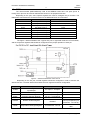
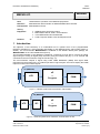
1 Introduction
The objective of this laboratory is to understand how to operate some of the programmable
interfaces available on a microcontroller (specifically on the MSP430 family, part number F5437 or
G2553). The microcontroller MSP430F5437 is available on the WSN4U board (from epfl/lap), the
MSP430G2553 on the LaunchPAD board (from ti)
The final demonstration of this laboratory (divided in 3 sessions) is to be able to convert an analog
signal using an Analog to Digital (A/D) converter (using the internal A/D (fig. 1) or an external A/D
connected to the microcontroller using the SPI bus (fig. 2)).
The microcontroller outputs a signal using Pulse Width Modulation (PWM) with signal width
proportional to the analog input. An oscilloscope and/or Logic Analyzer are used to display the PWM
output as well as other useful signals.
uC (MSP430)
uP
+
Program
ATD
PWM
Figure 1 – General system block schematic, internal ADC
uC (MSP430)
ATD
SPI
uP
+
Program
PWM
Figure 2 – General system block schematic, external ADC on SPI
R.Beuchat
E:\Users\Rene\rb-laboratories\trunk\Enonces_Doc\MSP430_LaboDocuments\Labo_MSP430_2_0.docx
Créé le 18/09/14
Modifié le 18/09/14 22:09
Impression le 18/09/14
Version [1.4]
Processor Architecture Laboratory
EPFL
MSP430
2
1.1
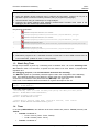
Clock (Unified clock System)
The explanations are done for the MSP430F5437 version. Search on the documentation the
difference for the MSP430G2553.
000
0
000
32'768Hz
000
32'768Hz
000
32'768Hz
0
32'768Hz
32'768Hz
000
100
11
11
000
100
000
0000011111 à
/(31+1)
1.048576 MHz
= 2 * (31+1) * 32'768 / 1
= D * (N +1) * FLLREFCLK/REFDIV
0
001
100
2.097152 MHz
1.048576 MHz
100
000
0
(Not used at reset)
1.048576 MHz
1
Figure 3 – Unified Clock System (UCS) block schematic MSP430F5437
An oscillator of 32’768 Hz is connected on input P7.0 and P7.1, so these pins are not available for
other purposes. That’s the XIN/XOUT quartz connection for XT1CLK in the TI documentation.
A high frequency signal (16 MHz - XT2) could be connected to the pins P5.2 and P5.3, but it is not
available in the WSN4U board.
The FLL (Frequency Locked Loop) is able to change the frequency of the FLLREFCLK input with a
Digitally-Controlled Oscillator (DCO).
The DCOCLK and DCOCLKDIV frequencies are given by:
fDCOCLK./ D = (N + 1) × (fFLLREFCLK / n)
fDCOCLKDIV = (N + 1) × (fFLLREFCLK / n)
R.Beuchat
reset : fDCOCLK = 2.097152 MHz
reset : fDCOCLKDIV =1.048576 MHz à MCLK, SMCLK
E:\Users\Rene\rb-laboratories\trunk\Enonces_Doc\MSP430_LaboDocuments\Labo_MSP430_2_0.docx
Processor Architecture Laboratory
EPFL
MSP430
3
with :
D : 1, 2, 4, 8, 16 or 32
N : 1..1023
n : 1, 2, 4, 8, 12, 16
(UCSCTL2: FLLD bits 14..12)
reset : 001 à * 2
(UCSCTL2: FLLN bits 9..0)
reset : 000011111 à * (31 +1)
(UCSCTL3: FLLREFDIV bits 2..0) reset : 000 à / 1
The figure 1 presents the general view of the unified clock system block and the reset default values
for the MSP430F5437 version. The registers are UCSCTL0 à UCSCTL8.
The OSC block (top left in the figure) could output 3 frequency signals:
XT1CLK
32’768 Hz from external quartz
VLOCLK
~10 kHz Low frequency
REFOCLK
32’768 Hz, internally generated Clk (used by default) à reset on ACLK
The FLL block (middle left in the figure) could output 2 frequency signals:
DCOCLK
DCOCLKDIV à DCOCLK divided by 1, 2, 4, 8,16 or 32, depending on FLLD register
Figure 4 – Unified Clock System (UCS) block schematic MSP430F2xx
MSP430G2xx3: LFXT1 does not support HF mode, XT2 is not present, ROSC is not supported.
R.Beuchat
E:\Users\Rene\rb-laboratories\trunk\Enonces_Doc\MSP430_LaboDocuments\Labo_MSP430_2_0.docx
Processor Architecture Laboratory
EPFL
MSP430
4
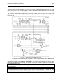
1.2
GPIO
The microcontroller (MSP430F5437) used in the WSN4U board has 8 I/O ports (Port1 to
Port8), which pins can be used as standard I/O function or as peripheral function.
Depending on the port, some specific registers are used to configure the pin function. The
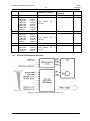
table below summarizes the shared functions for the MSP430F5437 microcontroller:
Port
Primary Function
Peripheral Functions
Port 1
I/O (P1.0 to P1.7)
Timer
Port 2
I/O (P2.0 to P2.7)
Timer, A/D converter, DMA trigger
Port 3
I/O (P3.0 to P3.7)
SPI, I2C, UART
Port 4
I/O (P4.0 to P4.7)
Timer
Port 5
I/O (P5.0 to P5.7)
SPI, I2C, A/C reference
Port 6
I/O (P6.0 to P6.7)
A/D converter
Port 7
I/O (P7.0 to P7.7)
Timer, A/D converter
Port 8
I/O (P8.0 to P8.6)
Timer
The figure 4 below illustrates how a typical I/O port is organized inside the microcontroller,
and the respective registers that should be configured for the proper operation of each pin:
Figure 5 – Internal architecture of the Port 8
Depending on the I/O port, several registers should be configured in order to achieve the
desired function. The table below summarizes the main registers and their configuration.
Register
Description
Configuration
PxDIR
Direction Register –
Input/Output
0à Input, 1 à Output
Comments
PxIN
Read Value Register
0à Low, 1 à High
PxOUT
Write Value Register
0à Low, 1 à High
PxSEL
Function Selection Register
0à I/O, 1à Peripheral
PxREN
Resistor Enable Register
0à Disabled, 1à
Enabled
If enabled, PxOUT
select pull-up/down (0à
Pull-down, 1à Pull-up)
PxDS
Output Drive Strength Register
0à Reduced, 1à Full
Full drive can increase
EMI
* In the table above, (x) represents a specific register (for Port 1, P1)
R.Beuchat
E:\Users\Rene\rb-laboratories\trunk\Enonces_Doc\MSP430_LaboDocuments\Labo_MSP430_2_0.docx
Processor Architecture Laboratory
5
Manipulation 1
EPFL
MSP430
GPIO
Using the WSN4U board schematic and TI MSP430 documentation, program an I/O port to
generate a pulse of minimum width by software (using C programming language)
Test the solution using an oscilloscope or a logic analyzer.
Compare the results obtained using software measurements (counting clock cycles in the
Debugger) and the oscilloscope measurements.
Required Documentation:
o
MSP430x5xx family full documentation, User's GuideFile
http://moodle.epfl.ch/pluginfile.php/1580215/mod_resource/content/1/Doc_composants/MSP430x2xx_slau144j.pdf
o
MSP430x2xx family full documentation, User's GuideFile
http://moodle.epfl.ch/pluginfile.php/1580215/mod_resource/content/1/Doc_composants/MSP430x2xx_slau144j.pdf
o
MSP430F543x Datasheet from tiFile
http://moodle.epfl.ch/pluginfile.php/902181/mod_resource/content/1/Doc_composants/MSP430F543x_Datasheet_slas612c-2.pdf
o
MSP430G3xx Datasheet from tiFile
http://moodle.epfl.ch/pluginfile.php/1580216/mod_resource/content/2/Doc_composants/msp430g2553.pdf
Manipulation 2
GPIO - Chenillard
Elaborate a program to do a “chenillard” function on Port8: bits 1 to 6 on WSN or Port2: bits 0 to
5 on LaunchPAD,. (rotation of value ‘1’ in the port bits).
1.3
Watch Dog Timer
During the procedure of power up, a watchdog timer is initiated. After ~32 ms the watchdog timer
will reset the CPU if not serviced. A specific access needs to be done before a programmable
expiration time.
For debugging purposes, it is recommended to deactivate the watchdog.
The WDTCTL register is a password protected register used in the configuration of the watchdog
timer. Any read/write operation in the WDTCTL register must use word instructions, and write
accesses must include the write password 0x5A (WDTPW) in the upper byte:
Have a look on the MSP430 full documentation for registers descriptions and use.
; Stop the watchdog timer
WDTCTL = WDTPW+WDTHOLD;
Some other useful selections:
; Periodically clear an active watchdog and specify the delay for next period
WDTCTL = WDTPW+WDTIS2+WDTIS1+WDTCNTCL;
; Change watchdog timer interval
WDTCTL = WDTPW+WDTCNTCL+SSEL;
; Change WDT to interval timer mode, clock/8192 interval, clear counter
WDTCTL = WDTPW+WDTCNTCL+WDTTMSEL+WDTIS_8192;
1.4
Timer
In the family MSP430F5437, two different 16-bit timer modules are present: TimerA (2 blocks) and
TimerB:
TimerA0 is available on :
o Port1.5..Port1.0 (TA0.4..TA0.0, TA0Clk)
o Port8.4..Port8.0 (TA0.4..TA0.0)
TimerA1 is available on :
R.Beuchat
E:\Users\Rene\rb-laboratories\trunk\Enonces_Doc\MSP430_LaboDocuments\Labo_MSP430_2_0.docx
Processor Architecture Laboratory
o
o
o
EPFL
MSP430
6
Port2.3..Port2.0 (TA1.2..TA1.0, TA1Clk),
Port7.3 (TA1.2)
Port8.6..Port8.5 (TA1.1..TA1.0)
TimerB is available on :
o Port4.7..Port4.0 (TB0Clk, TB6..TB0)
Port8
Port1
TimerA0
Port8-7
Port2
TimerA1
Port4
TimerB0
CCIxB
CCIxA
Input
Capture
CCIxB
CCIxA
Input
Capture
CCIxA/CCIxB
Input
Capture
P1.0
TA0Clk
P2.0
TA1Clk
P4.0
TB0.0
P8.0
P1.1
TA0.0
P8.5
P2.1
TA1.0
P4.1
TB0.1
P8.1
P1.2
TA0.1
P8.6
P2.2
TA1.1
P4.2
TB0.2
P8.2
P1.3
TA0.2
P7.3
P2.3
TA1.2
P4.3
TB0.3
P8.3
P1.4
TA0.3
P4.4
TB0.4
P8.4
P1.5
TA0.4
P4.5
TB0.5
P4.6
TB0.6
P4.7
TB0Clk
If the Input Capture mode is used, the user should select the source of the input signal, as for Timer
A there are 2 sources (pins) available (CCIxA and CCIxB).
As an output with Timer functionality, the corresponding bit in the GPIO PxSEL must be
programmed for the associated peripheral mode and not GPIO, this for each corresponding bit as ‘1’,
by default the GPIO mode is selected!
Port1
TimerA0
Port2
TimerA1
CCIxA
Input
Capture
CCIxA
Input
Capture
P1.0
TA0Clk
P2.0
TA1.0
P1.1
TA0.0
P2.1
TA1.1
P1.2
TA0.1
P2.2
TA1.1
P2.3
TA1.0
P2.4
TA1.2
P2.5
TA1.2
P1.5
TA0.0
P1.6
TA0.1
Figure 6 –Pinning og MSP430G2x53, 20 pins
R.Beuchat
E:\Users\Rene\rb-laboratories\trunk\Enonces_Doc\MSP430_LaboDocuments\Labo_MSP430_2_0.docx
Processor Architecture Laboratory
7
1.4.1
EPFL
MSP430
TimerA used as counter
The main block of the Timer Module is a 16-bit free running counter that can be configured to count
up or down (TAxR). The TAxCCRy register is used to compare a desired value with the free running
counter (0xFFFF is the maximum upper value).
The TAxCCRy CCIFG flag is used to indicate when the counter reach the desired value, and could
generate an interruption if properly configured. The figure 3 below shows the general architecture of
the Timer unit:
Figure 7 – Timer A block schematic (from TI)
By using the Compare function, a delay can be easily programmed. The clock dividers can
be used in order to achieve a desired counting range.
As exercise and using the Compare functionality, you have to write a function that has a delay
parameter as input (in number of ms]), that program correctly the TAxCCR register and actively polls
the Compare CCIFG Flag.
The MSP430G2 has only TimerA functionality. search on the User Manual the differences and the
pins assignment
Manipulation 3
TimerA0, delay
Use the TimerA1 to realize a delay function where the input parameter is a delay in [ms].
Program this function using the CCR comparator
R.Beuchat
E:\Users\Rene\rb-laboratories\trunk\Enonces_Doc\MSP430_LaboDocuments\Labo_MSP430_2_0.docx
Processor Architecture Laboratory
8
1.4.2
EPFL
MSP430
PWM generation
Use the TimerB0 to generate periodic pulse with pulse width modulation (PWM mode).
A period of ~10 [ms] is to be generated and the duty cycle should be programmed as a function
parameter. Study the different modes available on the Timer B to generate a PWM pulse.
Figure 8 TimerB block schematic (from ti)not available on G2
Manipulation 4
TimerB0, PWM or TimerA for G2553
Use the TimerB0 to generate a PWM pulse, using the CCR comparator to operate in the proper
manner. The PWM pulse must have a period of ~10[ms]. Use an oscilloscope to view and
validate the results.
R.Beuchat
E:\Users\Rene\rb-laboratories\trunk\Enonces_Doc\MSP430_LaboDocuments\Labo_MSP430_2_0.docx
Processor Architecture Laboratory
EPFL
MSP430
9
1.5
TimerA0 with interruption
It is possible to use the TimerA0 with Output compare function to generate a periodic interruption.
A vector table has the address of every interrupt routine that needs to be called for a specific
Interrupt Request. The address for the TimerA0 is 0xFFEC (entry 54 in decimal). Each entry is 16
bits and the table start at address 0xFF80 (so 0xFF80 + 2*54 = 0xFFEC).
A specific compilation pragma is used by the compiler to specify the interrupt service routine and the
corresponding vector address.
The entry points for the interruption vectors are specified in the msp430f5437.h file:
#define TIMER0_B0_VECTOR
#define TIMER0_B1_VECTOR
(60 * 1u)
(59 * 1u)
/* 0xFFF8 Timer0_B7 CC0 */
/* 0xFFF6 Timer0_B7 CC1-6, TB */
#define TIMER0_A0_VECTOR
#define TIMER0_A1_VECTOR
*/
(54 * 1u)
(53 * 1u)
/* 0xFFEC Timer0_A5 CC0 */
/* 0xFFEA Timer0_A5 CC1-4, TA0
#define TIMER1_A0_VECTOR
#define TIMER1_A1_VECTOR
*/
(49 * 1u)
(48 * 1u)
/* 0xFFE2 Timer1_A3 CC0 */
/* 0xFFE0 Timer1_A3 CC1-2, TA1
Specification of an interrupt routine in Code Composer 4:
#pragma vector=TIMER0_A1_VECTOR
__interrupt void TimerA0(void)
{
// something to do…
TA0CTL &= (~TAIFG);
// Interruption function for TAIFG
// Clear TAIFG flag in TA0CTL register
}
In order to enable global interrupts, the following instruction must be executed:
__bis_SR_register(GIE);
Manipulation 5
// Enter global Interrupt
Interruption on TimerA0
Use the TimerA0 to generate periodic interrupt of ~50[ms].. Toggle a GPIO on each interrupt.
Use an oscilloscope to view and validate the results.
Figure 9 TimerA/B Interrupt Request/Ack block schematic TAxCCR0 / TBxCCR0 (from ti)
Same functionality for the other CCRn.
R.Beuchat
E:\Users\Rene\rb-laboratories\trunk\Enonces_Doc\MSP430_LaboDocuments\Labo_MSP430_2_0.docx
Processor Architecture Laboratory
EPFL
MSP430
10
Timer interrupt vectors
Vector address
= 0xFF80 + 2* Priority
Symbol
= Priority
CCIFG0
0xFFF8
TIMER0_B0_VECTOR
60
Highest active
TB0CCR1:
TB0CCR2:
TB0CCR3:
TB0CCR4:
TB0CCR5:
TB0CCR6:
TB0CTL;
in TB0IV:
CCIFG1
CCIFG2
CCIFG3
CCIFG4
CCIFG5
CCIFG6
TBIFG
0xFFF6
TIMER0_B1_VECTOR
59
TA0CCR0:
CCIFG0
0xFFEC
TIMER0_A0_VECTOR
54
TIMER0_A1_VECTOR
53
Timer
Source
TB0
TB0CCR0:
TB0
TA0
TA0
TA1
TA1
1.5.1
One address
sources
for
Name Priority
7
Highest active
TA0CCR1:
TA0CCR2:
TA0CCR3:
TA0CCR4:
TA0CTL :
in TA0IV :
CCIFG1
CCIFG2
CCIFG3
CCIFG4
TAIFG
0xFFEA
TA1CCR0:
CCIFG0
0xFFE2
TIMER1_A0_VECTOR
49
0xFFE0
One address
sources
TIMER1_A1_VECTOR
48
Highest active
TA1CCR1:
TA1CCR2:
TA1CTL :
in TA1IV :
CCIFG1
CCIFG2
TAIFG
One address
sources
for
for
5
3
General Interruption architecture
Figure 10 - General interruption architecture (from TI)
R.Beuchat
E:\Users\Rene\rb-laboratories\trunk\Enonces_Doc\MSP430_LaboDocuments\Labo_MSP430_2_0.docx
Processor Architecture Laboratory
11
1.5.2
EPFL
MSP430
General Interruption architecture
Figure 11 - General interrupt architecture (fromTI)
(1) Multiple source flags
(2) A reset is generated if the CPU tries to fetch instructions from within peripheral space or vacant memory
space.
(Non)maskable: the individual interrupt-enable bit can disable an interrupt event, but the general-interrupt
enable cannot disable it.
(3) Interrupt flags are located in the module.
(4) Reserved interrupt vectors at addresses are not used in this device and can be used for regular program
code if necessary. To maintain compatibility with other devices, it is recommended to reserve these locations.
R.Beuchat
E:\Users\Rene\rb-laboratories\trunk\Enonces_Doc\MSP430_LaboDocuments\Labo_MSP430_2_0.docx
Processor Architecture Laboratory
12
1.6
EPFL
MSP430
ADC
The following manipulation intends to read an analog value from a potentiometer, using one of the
following methods:
Using the internal A/D programmable interface of the MSP430 microcontroller, with a
potentiometer connected to an I/O port.
Using an external extension A/D board that communicates through SPI bus
1.6.1
ADC on MSP430
The MSP430F5437 microcontroller has 12 input channels that can be sampled by a 12-bit internal
A/D converter (A15..A12 on Port7.7..Port7.4 and A7..A0 on Port6), and could be used to measure
4 internal voltages.
In order to program the A/D module, take a look on the TI documentation in order to perform a single
conversion on one channel with an external potentiometer connected to it..
Figure 12 – ADC12 module block schematic (fromTI)
Nice to study and use! Isn’t it ?
R.Beuchat
E:\Users\Rene\rb-laboratories\trunk\Enonces_Doc\MSP430_LaboDocuments\Labo_MSP430_2_0.docx
Processor Architecture Laboratory
13
1.6.2
EPFL
MSP430
External ADC using SPI
Using this option, an external board that contains the ADC124S051 A/D is used. The
ADC124S051 is a 12-bit Analog to Digital Converter; it has 4 input channels, and uses SPI bus in
order to output the analog value. The challenge in this case is to properly set-up the SPI
communication and to control the A/D channels to start the conversion.
In order to connect the extension A/D board to the microcontroller, we should use a specific
cable shown in the figure 8 below:
Figure 13 – Connection between the external A/D board and the microcontroller
Required Documentation:
ADC124S051 Datasheet:
http://moodle.epfl.ch/mod/resource/view.php?inpopup=true&id=437311
A/D extension board schematic
http://moodle.epfl.ch/mod/resource/view.php?id=437321
Manipulation 6
1.7
ADC, Analogue to Digital Converter
Select one of the 2 methods to acquire an analog signal from an external potentiometer and
write the corresponding function to do so.
ADC to control PWM
The objective of this section is to use the A/D value to control the PWM duty. The A/D converter
should be read every ~50ms. The conversion period should be done using interruptions.
Manipulation 7
Timer, ADC, PWM, GPIO and interruption
Use interruption to enable the ADC converter in order to start a conversion of the potentiometer
value (internal ADC12 module or external A/D with SPI interface).
Use another interruption routine to catch the result and change the PWM value accordingly.
Make a demo to an assistant, and display the result on an oscilloscope
R.Beuchat
E:\Users\Rene\rb-laboratories\trunk\Enonces_Doc\MSP430_LaboDocuments\Labo_MSP430_2_0.docx