1
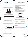
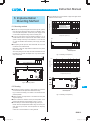
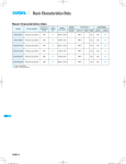
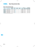
Basic Characteristics Data
Basic Characteristics Data
Model
Circuit method
Switching
frequency
[kHz]
Input
current
[A]
Rated
input fuse
Inrush
current
protection
circuit
Material
SNDBS400B
Forward converter
370
1.72 *1
450V 5A
-
SNDBS700B
Forward converter
381
2.76 *1
450V 10A
-
*1 Refer to specification.
*2 Refer to Instruction Manual.
SNDBS
SNDBS-6
Series/Parallel
operation availability
PCB/Pattern
Single
sided
Double
sided
Series
operation
Parallel
operation
FR-4
Yes
Yes
Yes*2
FR-4
Yes
Yes
Yes*2
DC-DC Converters Bus Converter . Power Module Value-added Type
Instruction Manual
1
Terminal Connection
SNDBS-8
2
Connection for Standard Use
SNDBS-8
3
Wiring Input / Output Terminal
SNDBS-9
4
3.1
Wiring input terminal
SNDBS-9
3.2
Wiring output terminal
SNDBS-9
Function
Overcurrent protection
SNDBS-10
4.2
Overvoltage protection
SNDBS-10
4.3
Thermal detection / Thermal protection
SNDBS-10
4.4
Inverter operation monitor (IOG)
SNDBS-10
4.5
Enable signal (ENA)
SNDBS-10
4.6
Remote ON / OFF (RC2)
SNDBS-11
4.7
Remote sensing
SNDBS-11
4.8
Output voltage adjusting
SNDBS-11
4.9
Isolation
SNDBS-11
4.1
5
6
SNDBS-10
Series and Parallel operation
SNDBS-12
5.1
Series operation
SNDBS-12
5.2
Parallel operation / Master-slave operation
SNDBS-12
5.3
N+1 Redundancy operation
SNDBS-12
Implementation-Mounting Method
SNDBS-13
6.1
Mounting method
SNDBS-13
6.2
Derating
SNDBS-13
SNDBS-7
SNDBS
DC-DC Converters Bus Converter . Power Module Value-added Type
1 Terminal Connection
Table 1.7 Terminal connection and functions of CN8
Pin No.
1
CN7
CN8
CN6
CN5
CN4 CN3
CN2
1 3 1 3
4
1
4
1
1
5 1
5
1
3
2
1
Function
Set short-piece to 1 and 2 when ENA is
Setting of ENA Enable (at shipping from factory)
Set short-piece to 2 and 3 when ENA
effective
is Disable
TB1
4
4
3
2
1
CN1
Instruction Manual
Short-piece for setting is attached on CN8 at shipping from factory
Table 1.8 Mating connectors and terminals of CN1,CN2,CN3,CN4,CN5 and CN6
Mating
Connector
Table 1.1 Terminal connection and functions
Terminal
connection
+VOUT
-VOUT
No
12
34
CN1
CN2
B3P4-VH-B
VHR-4N
CN3
B4B-XH-AM
XHP-4
CN4
B3B-XH-AM
XHP-3
CN5
CN6
B5B-XH-AM
XHP-5
Mfr.
Reel :SVH-21T-P1.1
Loose:BVH-21T-P1.1
Reel :SXH-001T-P0.6
Loose:BXH-001T-P0.6
J.S.T.
Reel :SXH-001T-P0.6
Function
+DC output
-DC output
Terminal
connector
Loose:BXH-001T-P0.6
Reel :SXH-001T-P0.6
Loose:BXH-001T-P0.6
Table 1.2 Configuration and functions of CN1 and CN2
Pin No.
1
2
3
4
ENA-B
-VIN
NC
+VIN
Function
: Enable signal
: -DC input
: No connection
: +DC input
Housing for protection is attached on CN2 at shipping from factory
2 Connection for Standard Use
¡In order to use the power supply, it is necessary Fig.2.1.
Table 1.3 Configuration and functions of CN3
Pin No.
1
+M
2
3
+S
-S
-M
4
DC power
supply +V
Function
: +Self sensing terminal.
(Do not wire for external connection.)
: +Remote sensing
: -Remote sensing
: -Self sensing terminal.
(Do not wire for external connection.)
SNDBS
-V
+V
+V
-V
-V
DC OUT
ENA FG
*Set short-piece to 2 and 3 on CN8
Short-pieces for without remote sensing is attached on CN3 at shipping from factory
(a) Connection for DC input
Table 1.4 Terminal connection and functions CN4
Pin No.
1
2
3
SNDBS
Function
RC2
: Remote ON/OFF
TEMP : Thermal detection / Thermal protection
IOG
: Inverter operation monitor
Table 1.5 Terminal connection and functions of CN5 and CN6
Pin No.
1
2
3
4
5
+S
-S
TRM
VB
CB
Function
: +Remote sensing
: -Remote sensing
: Adjustment of output voltage
: Voltage balance
: Current balance
SNDPF1000
AC IN
FG
SNDBS
AC(L) +V
+V
+V
AC(N) -V
-V
-V
FG
ENA
ENA FG
*Set short-piece to 1 and 2 on CN7 for using
with SNDPF1000
*Set short-piece to 2 and 3 on CN7 for using
with SNDPG750
*Refer to 4.5 Enable (ENA)
(b) Connection for AC input
Common signs among CN4 and CN5 represent the same potential.
Fig.2.1 Connection for Standard Use
Table 1.6 Terminal connection and functions of CN7
Pin No.
1
2
Function
S e t t i n g o f Set short-piece to 1 and 2 with SNDPF1000
Set short-piece to 2 and 3 with SNDPG750
ENA
Short-piece for setting is attached on CN7 at shipping from factory
SNDBS-8
DC OUT
¡ The SNDBS Series handles only the DC input.
Avoid applying AC input directly.
It will damage the power supply.
DC-DC Converters Bus Converter . Power Module Value-added Type
Instruction Manual
¡ Between the same terminal name, CN2 CN1 are power supply are
connected internally. Be used in multiple units can be cascaded.
Input voltage range
Input current [A]
Keep drawing current per pin below 7A for CN1/CN2.
¡ Operate with the conduction cooling(e.g. heat radiation from the
aluminum base plate to the attached heat sink).
Reference: 6.2 ”Derating”
¡ Please contact us If you need except SNDPG750/SNDPF1000 for
the input .
Ip
Input voltage [V]
3 Wiring Input / Output
Terminal
Fig.3.2 Input current characteristics
DC
3.1 Wiring input terminal
SNDBS
Load
SNDBS
Load
SNDBS
Load
AC
(1) External capacitor on the Input side
¡ When it turns on an input with a switch directly, one several times
the surge voltage of input voltage occurs by the inductance ingre-
AC
Rectifier
dient of an input line, and there is a possibility that a power supply
may break down.
Please install a capacitor between +VIN and -VIN input terminals
Fig.3.3 Use wit AC input
and absorb surge.
Capacitor : 47μF or more
(a)
¡ When the line impedance is high or the input voltage rise quickly
at start-up (less than 10μs), install a capacitor between +VIN and
(b)
SNDBS
SNDBS
+VIN
+VIN
Di Di
-VIN input terminals.
¡ Install a correspondence filter, if a noise standard meeting is required or if the surge voltage may be applied to the unit.
-VIN
Please contact us in details.
-VIN
Fig.3.4 Reverse input voltage protection
(2) Input voltage rang/Input current range
¡ The specification of input ripple voltage is 40Vp-p.
3.2 Wiring output terminal
¡ Make sure that the voltage fluctuation, including the ripple voltage, will not exceed the input voltage range.
¡ Use a front end unit with enough power, considering the start-up
current Ip of this unit.
¡ The specified ripple and ripple noise are measured by the method
introduced in Fig.3.5.
100mm
(3) Operation with AC input
SNDBS
¡ The SNDBS series handles only for the DC input.
A front end unit(AC/DC unit) is required when the SNDBS series
+VIN +VOUT
+M
is operated with AC input.
(4) Reverse input voltage protection
¡ Avoid the reverse polarity input voltage. It will break the power
supply.
It is possible to protect the unit from the reverse input voltage by
Ripple
Time
Fig.3.1 Ripple of input voltage
ψ t
Input voltage range
Input voltage
installing an external diode.
Measuring
bord
SNDBS
+S
DC
Input
0.1µF
Load
-S
-M
-VIN
Oscilloscope
BW : 100MHz
-VOUT
R
1.5m 50W
Coaxial Cable
C
R=50W
C=0.01µF
Fig.5.1 Method of Measuring Output Ripple and Ripple Noise
SNDBS-9
DC-DC Converters Bus Converter . Power Module Value-added Type
Instruction Manual
4.4 Inverter operation monitor (IOG)
4 Function
¡ By using the inverter operation monitor(IOG), malfunction of the
inverter can be monitored.
When inverter operation is in following mode or , IOG signal turns
4.1 Overcurrent protection
H” from L” within 1 second.
¡Overcurrent protection is built-in and comes into effect at over
105% of the rated current.
Overcurrent protection prevents the unit from short circuit and
overcurrent condition. The unit automatically recovers when the
fault condition is cleared.
¡ When the output voltage drops at overcurrent, the average output
current is reduced by intermittent operation of power supply
IOG circuit is designed as shown in Fig.4.1 and specification is
shown in Table 4.1.
1Malfunction of inverter.
2The output voltage drops by 60% or less of the rated voltage.
3When output wattage is decreased radically to less than 10% of
rated wattage.
4.5 Enable signal (ENA)
4.2 Overvoltage protection
¡ The overvoltage protection circuit is built-in. The DC input should
be shut down if overvoltage protection is in operation. The minimum interval of DC recycling for recovery is for 2 to 3 minutes(*).
*The recovery time varies depending on input voltage and input
capacity.
¡ When I connect SNDPF or SNDPG to input of SNDBS, you can
operate it to start, a stop of SNDPF by connecting ENA.
In this case, please set the short-piece of CN8 on 1 pin and 2
pins to prevent the trouble of the power supply.
¡ When the power supplies are shipped from a factory, they come
with a dedicated short-piece being mounted on CN7.
If you use SNDPF1000 , you can use the power supplies as they
Remarks:
are.
Please note that devices inside the power supply might fail when
If you use SNDPG750 , you must set short-piece to pin2 and 3 on
voltage more than rated output voltage is applied to output termi-
CN7.
nal of the power supply. This could happen when the customer
Short-piece
Short-piece
tests the overvoltage performance of the unit.
CN7
CN7
4.3 Thermal detection / Thermal protection
¡ Thermal detection (TMP) and protection circuit are built-in.
¡ When overheat is detected, thermal detection signal (TMP) turns
1
2
3
1
2
3
”L” from ”H”. TMP circuit is designed as shown in Fig.4.1, and
specification is shown as in Table 4.1.
¡ When overheating continues after detecting the TMP signal, the
output will be shut down by the thermal protection circuit.
ENA terminal Enable
(at shipping from factory)
ENA terminal Disable
Fig.4.2 Setting of ENA
When this function comes into effect, input voltage should be shut
off, and eliminate all possible causes of overheat condition and
lower the temperature of the unit to the normal level.
¡ If you do not use ENA , remove the short-piece to pin 2 and 3 at
CN8 shown in Fig.4.3.
Short-piece
Short-piece
22kW
SNDBS
TMP or IOG
6V typ
CN8
CN8
-S
1
Fig.4.1 TMP, IOG circuit
Table 4.1 Specification of TMP, IOG
No.
Item
1
Function
2
3
4
5
6
Base pin
Level voltage “L “
Level voltage “H”
Maximum sink current
Maximum applicable voltage
SNDBS-10
TMP
Normal operation “H”
IOG
Normal operation “L”
Overheat detection “L”
Malfunction of inverter “H”
-S
0.5Vmax at 5mA
5V typ
10mA max
35V max
2
3
1
The ENA terminal is effective
(Initial setting)
2
3
The ENA terminal is invalid
Fig.4.3 Setting of ENA
DC-DC Converters Bus Converter . Power Module Value-added Type
Instruction Manual
¡ When the remote sensing function is used, the output voltage of
the power supply may show an oscillating waveform or the output
4.6 Remote ON / OFF (RC2)
¡ You can operate the remote ON/OFF function by sending signals
to CN4.
voltage may dramatically fluctuate because of an impedance of
wiring and load conditions.
Please see Table 4.2 for specifications.
¡ Remote ON/OFF circuits (RC2 ) is not isolated from output.
4.8 Output voltage adjusting
(1) Adjusting method by installed potentiometer
2.35KW
¡ Output voltage is adjustable by the internal potentiometer or by
applied voltage externally.
The adjustable range is 90 - 110% of the rated output voltage.
12V
typ
RC2
To increase an output voltage, turn a built-in potentiometer clock-
l1
-S OFF
wise.
POWER
ON
To decrease the output voltage, turn it counterclockwise
¡ The output adjustment range for DBS700B is shown in Fig.4.4.
110
Output voltage [%]
Fig.4.3 Remote ON/OFF (RC2)
Table 4.2 Specification of output side remote ON/OFF (RC2)
No.
1
2
3
Item
Power ON
Power OFF
Base pin
RC2
Open (0.1mA max)
Short (3mA min)
-S
105
100
60
0
0
200V
250
Input voltage [V]
Fig.4.4 SNDBS700B Output Voltage Adjustment Range
4.7 Remote sensing
(1) When the remote sensing function is not in use
(2) Adjusting method by applying external voltage
¡ If you do not use the remote sensing function, you can short out
between +S and +M and between -S and -M on CN3.
¡ By applying the voltage externally at TRM, output voltage become
adjustable.
When the power supplies are shipped from a factory, they come
Output voltage is calculated by the following equation.
with a dedicated harness being mounted on CN3.
If you do not use the remote sensing function, you can use the
Output voltage [V]=
power supplies as they are.
Applied voltage
externally [V]
XRated output voltage [V] 1
1 [V]
¡ If the output voltage decreases to almost 0V, output ripple may
become large.
(2) When the remote sensing function is in use
¡ Please see Fig.4.2 if you use the remote sensing function.
Wire as close as possible
¡ When the output voltage adjustment is used, note that the overvoltage protection circuit operates when the output voltage sets
too high.
4.9 Isolation
SNDBS
+S
+VOUT
+ Co
Load
-VOUT
-S
¡ For a receiving inspection, such as Hi-Pot test, gradually
increase(decrease) the voltage for a start(shut down). Avoid using Hi-Pot tester with the timer because it may generate voltage a
few times higher than the applied voltage, at ON/OFF of a timer.
Fig.4.2 Connection when the remote sensing is in use
¡ Wire carefully. When a connection of a load line becomes
loose(due to such factors as loose screw), the load current flows
to the sensing line and internal circuits of the power supply may
be damaged.
¡ Use a sufficiently thick wire to connect between the power supply
and the load and keep the line drop at 0.3V or below.
¡ Use a twisted pair wire or a shielded wire as the sensing line.
¡ Do not draw the output current from +M, -M, +S or -S.
SNDBS-11
SNDBS
DC-DC Converters Bus Converter . Power Module Value-added Type
5 Series and Parallel
Operation
Instruction Manual
¡ Connect the sensing line and the power line by one point after
connecting each power supply’s sensing pins(+S, -S).
In multiple operation, sensing wires should be connected between
each units for the muster connection to a load.
¡ Output current should be 10% or more of the total of the rated
output current in parallel operation. If less than 10%, the IOG signal might become unstable, and output voltage slightly increasing
5.1 Series operation
(max5%).
¡Series operation is available by connecting the outputs of two or
more power supplies, as shown below. Output current in series
¡ IOG signal might be unstable for one second when the units are
turned on in parallel operation.
connection should be lower than the lowest rated current in each
¡ Please be connected diode to the +VOUT side to avoid malfunctions and damage.
unit.
(a)
Power +
Supply -
Sensing point
Power +
Supply -
CN5
Load
Power +
Supply -
CB
VB
TRM
-S
+S
PS1(Master)
CN5
CB
VB
TRM
-S
+S
Load
PS2(Slave)
Power +
Supply -
+VOUT
CN3
+M
+S
-S
-M
Co
+
Load
-VOUT
CN6
CB
VB
TRM
-S
+S
(b)
CB
VB
TRM
-S
+S
Load
CN6
+VOUT
+M
+S
-S
-M
CN3
Open
Open
-VOUT
CB
VB
TRM
-S
+S
CN6
Fig.5.1 Serial operation
5.2 Parallel operation/Master-slave operation
¡ Parallel operation is available by connecting the units as shown in
Fig.5.2.
¡ You can adjust the output voltage in parallel operation by adjusting a potentiometer of just one power supply.
To do so, select one power supply as the master unit and turn the
potentiometers of the other (slave) power supplies clockwise to
the end.
Once you have done this, you can adjust the output voltage by
turning the potentiometer of the master unit.
SNDBS
¡ You cannot parallels operate power supplies with different output
voltage or electrical power.
¡ As variance of output current drew from each power supply is maximum 10%, the total output current must not exceed the value determined by the following equation.
Output current in
parallel operation
=
the rated current
per unit
X(number of unit)X0.9
In parallel operation, the maximum operative number of units is 5.
¡ When the number of the units in parallel operation increases,
input current increases. Adequate wiring design for input circuitry
such as circuit pattern, wiring and current for equipment is required.
Connect the sensing line and the power line by one point after
connecting each power supply’s sensing pins(+S, -S). In multiple
operation, sensing wires should be connected between each units
for the muster connection to a load.
SNDBS-12
CN5
CB
VB
TRM
-S
+S
PS3(Slave)
+VOUT
+M
+S
-S
-M
CN3
Open
Open
-VOUT
Fig.5.2 Examples of parallel operation
5.3 N+1 Redundancy operation
¡ It is possible to set N+1 redundant operation for improving reliability of power supply system.
Purpose of redundant operation is to ensure stable operation in
the event of single power supply failure.
Since extra power supply is reserved for the failure condition, so
total power of redundant operation is equal to N-1.
¡ Please contact us about N+1 redundant operation in details.
DC-DC Converters Bus Converter . Power Module Value-added Type
Instruction Manual
¡ In the hatched area, the specification of ripple and ripple noise is
different from other areas
6 ImplementationMounting Method
6.1 Mounting method
¡ When two or more power supplies are used side by side, position
them with proper intervals to allow enough air ventilation. Alumi-
Load factor [%]
100
num base plate temperature around each power supply should
2
1SNDBS400B
2SNDBS700B12,24,28
3SNDBS700B36,48
50
0
-20
-10
0
10
not exceed the temperature range shown in derating curve.
20
30
40
50
3
1
60 65 70
80
90 95 100
Temperature point A [C]
¡ In case of metal chassis, keep the distance between d1 for to
insulate between lead of component and metal chassis, use the
CN1
spacer of 4mm[0.16 inches] or more between d1. If it is less than
TB1
d1, insert the insulation sheet between power supply and metal
chassis.
¡ Avoid placing the DC input line wires underneath the unit, it will
increase the line conducted noise.
Make sure to leave an ample distance between the line pattern
Point A
lay out and the unit.
Measuring Point
Also avoid placing the DC output line wires underneath the unit
because it may increase the output noise. Lay out the pattern
Fig. 6.2 Derating curve (Point A)
d1
away from the unit.
d1
Load factor [%]
100
50
d1
0
-20
d1
-10
0
10
20
30
40
50
60
70
Temperature point B [C]
CN2
d1
TB1
Fig.6.1 Mounting method
CN1
SNDBS
6.2 Derating
¡ Use with the conduction cooling(e.g. heat radiation by conduction
from the aluminum base plate to the attached heat sink).
Point B (C51)
Measuring Point
Fig.6.2 shows the derating curve based on the aluminum base
plate temperature.
Fig. 6.3 Derating curve (Point A)
¡ Please measure the temperature on the aluminum base plate
edge side (Point A).
¡ Please consider the ventilation to keep the temperature on the
PCB (Point B) less than the temperature of Fig.6.3., Fig.6.5.
¡ It is necessary to note the thermal fatigue life by power cycle.
Please reduce the temperature fluctuation range as much as possible when the up and down of the temperature are frequently
generated.
Contact us for more information on cooling methods.
SNDBS-13