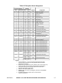
1
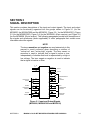
31
16 15
8 7
0
D0
D1
D2
D3
EIGHT
DATA
REGISTERS
D4
D5
D6
D7
31
16 15
0
A0
A1
A2
SEVEN
ADDRESS
REGISTERS
A3
A4
A5
A6
A7
USER STACK
(USP) POINTER
31
0
7
PC
PROGRAM
COUNTER
CCR
STATUS
REGISTER
0
Figure 2-1. User Programmer's Model
(MC68000/MC68HC000/MC68008/MC68010)
2.1.2 Supervisor Programmer's Model
The supervisor programmer's model consists of supplementary registers used in the
supervisor mode. The M68000 MPUs contain identical supervisor mode register
resources, which are shown in Figure 2-2, including the status register (high-order byte)
and the supervisor stack pointer (SSP/A7').
31
16 15
0
A7'
SUPERVISOR STACK
(SSP) POINTER
15
8 7
0
CCR
SR
STATUS REGISTER
Figure 2-2. Supervisor Programmer's Model Supplement
The supervisor programmer's model supplement of the MC68010 is shown in Figure 23. In addition to the supervisor stack pointer and status register, it includes the vector
base register (VRB) and the alternate function code registers (AFC).The VBR is used to
determine the location of the exception vector table in memory to support multiple vector
2-2
M68000 8-/16-/32-BIT MICROPROCESSOR USER’S MANUAL
MOTOROLA
tables. The SFC and DFC registers allow the supervisor to access user data space or
emulate CPU space cycles.
31
16 15
15
0
8 7
A7'
(SSP)
SUPERVISOR STACK
POINTER
SR
STATUS REGISTER
VBR
VECTOR BASE REGISTER
SFC
ALTERNATE FUNCTION
CODE REGISTERS
0
CCR
31
0
2
0
DFC
Figure 2-3. Supervisor Programmer's Model Supplement
(MC68010)
2.1.3 Status Register
The status register (SR),contains the interrupt mask (eight levels available) and the
following condition codes: overflow (V), zero (Z), negative (N), carry (C), and extend (X).
Additional status bits indicate that the processor is in the trace (T) mode and/or in the
supervisor (S) state (see Figure 2-4). Bits 5, 6, 7, 11, 12, and 14 are undefined and
reserved for future expansion
SYSTEM BYTE
15
13
T
S
USER BYTE
10
8
I2 I1 I0
4
X
0
N Z V
C
TRACE MODE
EXTEND
NEGATIVE
ZERO
OVERFLOW
CARRY
SUPERVISOR
STATE
INTERRUPT
MASK
CONDITION
CODES
Figure 2-4. Status Register
2.2
DATA TYPES AND ADDRESSING MODES
The five basic data types supported are as follows:
1. Bits
2. Binary-Coded-Decimal (BCD) Digits (4 Bits)
3. Bytes (8 Bits)
4. Words (16 Bits)
5. Long Words (32 Bits)
MOTOROLA
M68000 8-/16-/32-BIT MICROPROCESSOR USER’S MANUAL
2-3
SECTION 3
SIGNAL DESCRIPTION
This section contains descriptions of the input and output signals. The input and output
signals can be functionally organized into the groups shown in Figure 3-1 (for the
MC68000, the MC68HC000 and the MC68010), Figure 3-2 ( for the MC68HC001), Figure
3-3 (for the MC68EC000), Figure 3-4 (for the MC68008, 48-pin version), and Figure 3-5
(for the MC68008, 52-pin version). The following paragraphs provide brief descriptions of
the signals and references (where applicable) to other paragraphs that contain more
information about the signals.
NOTE
The terms assertion and negation are used extensively in this
manual to avoid confusion when describing a mixture of
"active-low" and "active-high" signals. The term assert or
assertion is used to indicate that a signal is active or true,
independently of whether that level is represented by a high or
low voltage. The term negate or negation is used to indicate
that a signal is inactive or false.
VCC(2)
GND(2)
ADDRESS
BUS
A23–A1
CLK
DATA BUS
D15–D0
PROCESSOR
STATUS
FC0
FC1
FC2
AS
R/W
UDS
LDS
DTACK
ASYNCHRONOUS
BUS
CONTROL
MC6800
PERIPHERAL
CONTROL
E
VMA
VPA
BR
BG
BGACK
BUS
ARBITRATION
CONTROL
SYSTEM
CONTROL
BERR
RESET
HALT
IPL0
IPL1
IPL2
INTERRUPT
CONTROL
Figure 3-1. Input and Output Signals
(MC68000, MC68HC000 and MC68010)
MOTOROLA
M68000 8-/16-/32-BIT MICROPROCESSORS USER'S MANUAL
3-1
Table 3-3. Function Code Outputs
Function Code Output
FC2
FC1
FC0
Address Space Type
Low
Low
Low
(Undefined, Reserved)
Low
Low
High
User Data
Low
High
Low
User Program
Low
High
High
(Undefined, Reserved)
High
Low
Low
(Undefined, Reserved)
High
Low
High
Supervisor Data
High
High
Low
Supervisor Program
High
High
High
CPU Space
3.9 CLOCK (CLK)
The clock input is a TTL-compatible signal that is internally buffered for development of
the internal clocks needed by the processor. This clock signal is a constant frequency
square wave that requires no stretching or shaping. The clock input should not be gated
off at any time, and the clock signal must conform to minimum and maximum pulse-width
times listed in Section 10 Electrical Characteristics.
3.10 POWER SUPPLY (V CC and GND)
Power is supplied to the processor using these connections. The positive output of the
power supply is connected to the VCC pins and ground is connected to the GND pins.
MOTOROLA
M68000 8-/16-/32-BIT MICROPROCESSORS USER'S MANUAL
3-9
3.11 SIGNAL SUMMARY
Table 3-4 summarizes the signals discussed in the preceding paragraphs.
Table 3-4. Signal Summary
Hi-Z
Signal Name
Input/Output
Active State
Address Bus
A0–A23
Output
High
Yes
Yes
Data Bus
D0–D15
Input/Output
High
Yes
Yes
AS
Output
Low
No
Yes
Read/Write
R/ W
Output
Read-High
Write-Low
No
Yes
Data Strobe
DS
Output
Low
No
Yes
UDS, LDS
Output
Low
No
Yes
DTACK
Input
Low
No
No
Bus Request
BR
Input
Low
No
No
Bus Grant
BG
Output
Low
No
No
BGACK
Input
Low
No
No
IPL 0, IPL 1,
IPL 2
Input
Low
No
No
Bus Error
BERR
Input
Low
No
No
Mode
MODE
Input
High
—
—
Reset
RESET
Input/Output
Low
No*
No*
HALT
Input/Output
Low
No*
No*
E
Output
High
No
No
Valid Memory Address
VMA
Output
Low
No
Yes
Valid Peripheral Address
VPA
Input
Low
No
No
FC0, FC1,
FC2
Output
High
No
Yes
Clock
CLK
Input
High
No
No
Power Input
VCC
Input
—
—
—
Ground
GND
Input
—
—
—
Address Strobe
Upper and Lower Data Strobes
Data Transfer Acknowledge
Bus Grant Acknowledge
Interrupt Priority Level
Halt
Enable
Function Code Output
On
HALT
Mnemonic
On Bus
Relinquish
*Open drain.
3-10
M68000 8-/16-/32-BIT MICROPROCESSORS USER'S MANUAL
MOTOROLA
4. For an MC68010, return DTACK before data verification. If data is invalid, assert
BERR on the next clock cycle (case 4).
Table 5-6.
BERR and HALT Negation Results
Negated on Rising
Edge of State
Conditions of
Termination in
Table 4-4
Control Signal
N
Bus Error
BERR
HALT
•
•
or
or
•
•
Takes bus error trap.
Rerun
BERR
HALT
•
•
or
•
Illegal sequence; usually traps to vector number 0.
Rerun
BERR
HALT
•
BERR
HALT
•
•
or
•
BERR
HALT
•
or
•
none
Normal
Normal
N+2
Results—Next Cycle
Reruns the bus cycle.
•
May lengthen next cycle.
If next cycle is started, it will be terminated as a bus
error.
• = Signal is negated in this bus state.
5.7 ASYNCHRONOUS OPERATION
To achieve clock frequency independence at a system level, the bus can be operated in
an asynchronous manner. Asynchronous bus operation uses the bus handshake signals
to control the transfer of data. The handshake signals are AS, UDS, LDS, DS (MC68008
only), DTACK, BERR, HALT, AVEC (MC68EC000 only), and VPA (only for M6800
peripheral cycles). AS indicates the start of the bus cycle, and UDS, LDS, and DS signal
valid data for a write cycle. After placing the requested data on the data bus (read cycle)
or latching the data (write cycle), the slave device (memory or peripheral) asserts DTACK
to terminate the bus cycle. If no device responds or if the access is invalid, external control
logic asserts BERR, or BERR and HALT, to abort or retry the cycle. Figure 5-31 shows the
use of the bus handshake signals in a fully asynchronous read cycle. Figure 5-32 shows a
fully asynchronous write cycle.
ADDR
AS
R/W
UDS/LDS
DATA
DTACK
Figure 5-31. Fully Asynchronous Read Cycle
5-32
M68000 8-/16-/32-BIT MICROPROCESSORS USER'S MANUAL
MOTOROLA
ADDR
AS
R/W
UDS/LDS
DATA
DTACK
Figure 5-32. Fully Asynchronous Write Cycle
In the asynchronous mode, the accessed device operates independently of the frequency
and phase of the system clock. For example, the MC68681 dual universal asynchronous
receiver/transmitter (DUART) does not require any clock-related information from the bus
master during a bus transfer. Asynchronous devices are designed to operate correctly
with processors at any clock frequency when relevant timing requirements are observed.
A device can use a clock at the same frequency as the system clock (e.g., 8, 10, or 12.5,
16, and 20MHz), but without a defined phase relationship to the system clock. This mode
of operation is pseudo-asynchronous; it increases performance by observing timing
parameters related to the system clock frequency without being completely synchronous
with that clock. A memory array designed to operate with a particular frequency processor
but not driven by the processor clock is a common example of a pseudo-asynchronous
device.
The designer of a fully asynchronous system can make no assumptions about address
setup time, which could be used to improve performance. With the system clock frequency
known, the slave device can be designed to decode the address bus before recognizing
an address strobe. Parameter #11 (refer to Section 10 Electrical Characteristics)
specifies the minimum time before address strobe during which the address is valid.
In a pseudo-asynchronous system, timing specifications allow DTACK to be asserted for a
read cycle before the data from a slave device is valid. The length of time that DTACK
may precede data is specified as parameter #31. This parameter must be met to ensure
the validity of the data latched into the processor. No maximum time is specified from the
assertion of AS to the assertion of DTACK. During this unlimited time, the processor
inserts wait cycles in one-clock-period increments until DTACK is recognized. Figure 5-33
shows the important timing parameters for a pseudo-asynchronous read cycle.
MOTOROLA
M68000 8-/16-/32-BIT MICROPROCESSORS USER'S MANUAL
5-33
Table 6-2. Exception Vector Assignment
Vectors Numbers
Address
Hex
Decimal
Dec
Hex
Space 6
0
0
0
000
SP
1
1
4
004
SP
Reset: Initial SSP2
Reset: Initial PC 2
2
2
8
008
SD
Bus Error
3
3
12
00C
SD
Address Error
4
4
16
010
SD
Illegal Instruction
Assignment
5
5
20
014
SD
Zero Divide
6
6
24
018
SD
CHK Instruction
7
7
28
01C
SD
TRAPV Instruction
8
8
32
020
SD
Privilege Violation
9
9
36
024
SD
Trace
A
10
40
028
SD
Line 1010 Emulator
B
11
44
02C
SD
Line 1111 Emulator
C
48
030
SD
(Unassigned, Reserved)
D
121
131
52
034
SD
(Unassigned, Reserved)
E
14
56
038
SD
Format Error 5
F
15
60
03C
SD
Uninitialized Interrupt Vector
10–17
16–231
64
040
SD
(Unassigned, Reserved)
92
05C
18
24
96
060
SD
Spurious Interrupt 3
19
25
100
064
SD
Level 1 Interrupt Autovector
—
1A
26
104
068
SD
Level 2 Interrupt Autovector
1B
27
108
06C
SD
Level 3 Interrupt Autovector
1C
28
112
070
SD
Level 4 Interrupt Autovector
1D
29
116
074
SD
Level 5 Interrupt Autovector
1E
30
120
078
SD
Level 6 Interrupt Autovector
1F
31
124
07C
SD
20–2F
32–47
128
080
SD
Level 7 Interrupt Autovector
TRAP Instruction Vectors4
188
0BC
30–3F
48–631
192
0C0
SD
(Unassigned, Reserved)
255
0FF
40–FF
64–255
256
100
1020
3FC
—
—
SD
User Interrupt Vectors
—
NOTES:
1. Vector numbers 12, 13, 16–23, and 48–63 are reserved for future
enhancements by Motorola. No user peripheral devices should be
assigned these numbers.
2. Reset vector (0) requires four words, unlike the other vectors which only
require two words, and is located in the supervisor program space.
3. The spurious interrupt vector is taken when there is a bus error
indication during interrupt processing.
4. TRAP #n uses vector number 32+ n.
5. MC68010 only. This vector is unassigned, reserved on the MC68000
and MC68008.
6. SP denotes supervisor program space, and SD denotes
supervisor data space.
MOTOROLA
M68000 8-/16-/32-BIT MICROPROCESSORS USER’S MANUAL
6-7