1
General Design Information
www.ti.com
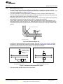
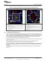
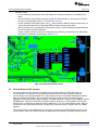
Some things to note about Figure 9:
• For the outer two rows of balls, all but four signals route on the top layer to escape the BGA.
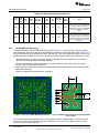
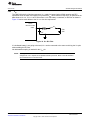
• Routing from the second row of balls between balls with a 0.5 mm (19.69 mil) spacing and 0.1 mm (4.0
mil) trace/space is not possible. Traces from the second row of balls must be routed through the
opening left by the depopulated ball in the first row as shown in Figure 10 where E is 0.1 mm (4 mil)
and F is 0.12 mm (4.76 mil).
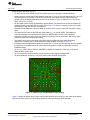
• All other balls require vias to the backside or power planes. The placement of the vias is important to
enable all traces on the back side to escape. See Figure 11. It may be necessary to use a very small
grid spacing to align the vias with 4 mil spacing.
• Each set of three balls that connect to GND on the three of the corners of the BGA can share a via to
GND.
• The balls near the center of the BGA are either power (VDD) or ground (GND). These balls are
connected together in a web-like structure with 6 mil wide traces to provide a low impedance
connection to power or ground. This web structure is preferred over a copper pour, which may cause
assembly issues due to uneven ball melting.
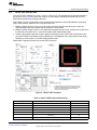
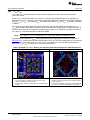
• The location of the vias in the center of the BGA allow for placement of two 0402 decoupling
capacitors on the back side of the board directly under the BGA, as shown in Figure 11.
• Impedance controlled differential signals are routed with 0.1 mm (4 mil) trace/spacing until they escape
the perimeter of the BGA and can be routed with the desired trace width and spacing to meet the
impedance target.
• All VDD, VDDA, GND, GNDA, VREFA+ and VREFA- signals are routed as 0.1524 mm (6 mil) traces
within the BGA escape area.
• All VDDC signals are routed as 0.2032 mm (8 mil) traces within the BGA escape area.
• All other signals are routes as 1 mm (4 mil) traces within the BGA escape area.
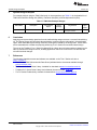
Figure 11. Bottom Layer 212-Ball BGA Escape Routing
Figure 11 shows the bottom layer escape routing under the BGA from the vias. In the center of the bottom
layer are two 0402 sized 0.1μF decoupling capacitors connected between VDD and GND.
SPMA056 – October 2013
Submit Documentation Feedback
System Design Guidelines for the TM4C129x Tiva™ C Series
Microcontrollers
Copyright © 2013, Texas Instruments Incorporated
13