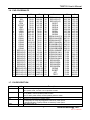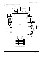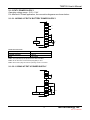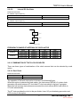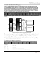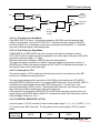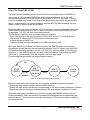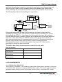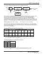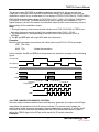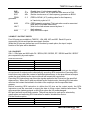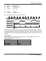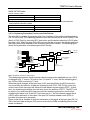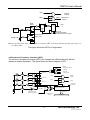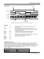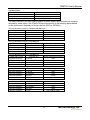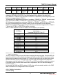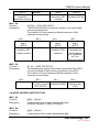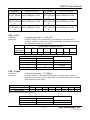
1
TM8705
4-Bit Micro-Controller
with LCD Driver
User’s Manual
tenx technology, inc.
tenx technology, inc.
Rev 1.2 2003/7/31
TM8705 User’s Manual
CONTENTS
CHAPTER 1 General Description ...................................................................3
1-1 General Description .......................................................................................................... 3
1-2 Features.............................................................................................................................. 4
1-3 Application.......................................................................................................................... 4
1-4 Block Diagram ................................................................................................................... 5
1-5 Pad Diagram ...................................................................................................................... 5
1-6 Pad Coordinate .................................................................................................................. 6
1-7 Pin Descriptions ................................................................................................................. 6
1-8 Characterization ................................................................................................................ 7
1-9 Typical Application Circuitry ..........................................................................................11
CHAPTER 2 TM8705 Internal System Architecture...................................12
2-1 Power Supply .................................................................................................................12
2-2 System Clock .................................................................................................................18
2-3 Program Counter (PC)..................................................................................................26
2-4 Program/Table Memory (ROM)...................................................................................27
2-5 Index Address Register (@HL) ...................................................................................29
2-6 Stack Register (STACK)...............................................................................................30
2-7 Data Memory (RAM) .....................................................................................................31
2-8 Working Register (WR).................................................................................................31
2-9 Accumulator (AC) ..........................................................................................................32
2-10 ALU (Arithmetic and Logic Unit) ...............................................................................32
2-11 Hexadecimal Convert to Decimal (HCD).................................................................32
2-12 Timer 1 (TMR1) ...........................................................................................................34
2-13 Timer 2 (TMR2) ...........................................................................................................36
2-14 Status Register (STS).................................................................................................41
2-15 Control Register (CTL) ...............................................................................................46
2-16 HALT Function.............................................................................................................50
2-17 Heavy Load Function..................................................................................................50
2-18 STOP Function ............................................................................................................52
1
tenx technology, inc.
Rev 1.2 2003/7/31
TM8705 User’s Manual
2-19 Back Up Function........................................................................................................53
CHAPTER 3 Control Function.......................................................................55
3-1 Interrupt Function ..........................................................................................................55
3-2 Reset Function...............................................................................................................59
3-3 Clock Generator, Frequency Generator and Predivider .........................................63
3-4 Buzzer Output Pins .......................................................................................................66
3-5 Input / Output Ports .......................................................................................................68
3-6 EL Panel Driver..............................................................................................................77
3-7 External INT Pin.............................................................................................................79
3-8 Resistor to Frequency Converter (RFC)....................................................................80
3-9 Key Matrix Scanning .....................................................................................................84
CHAPTER 4 LCD Driver Output....................................................................89
4-1 LCD Lighting System in TM8705 ................................................................................89
4-2 DC Output......................................................................................................................91
4-3 Segment PLA Circuit for LCD Display .......................................................................92
CHAPTER 5 Detail Explanation of TM8706 Instructions...........................98
5-1 Input / Output Instructions ............................................................................................98
5-2 Accumulator Manipulation Instructions and Memory Manipulation
Instructions ...................................................................................................................105
5-3 Operation Instructions .................................................................................................107
5-4 Load / Store Instructions ............................................................................................118
5-5 CPU Control Instructions ............................................................................................120
5-6 Index Address Instructions .........................................................................................123
5-7 Decimal Arithmetic Instructions .................................................................................124
5-8 Jump Instructions ........................................................................................................126
5-9 Miscellaneous Instructions .........................................................................................127
APPNDIX A TM8705 Instruction Table .................................................... 133
2
tenx technology, inc.
Rev 1.2 2003/7/31
TM8705 User’s Manual
Chapter 1 General Description
1-1.
GENERAL DESCRIPTION
The TM8705 is an embedded high-performance 4-bit microcomputer with LCD driver. It
contains all the necessary functions, such as 4-bit parallel processing ALU, ROM, RAM,
I/O ports, timer, clock generato r, dual clock operation, Resistance to Frequency
Converter(RFC), EL panel driver, LCD driver, look-up table, watchdog timer and key matrix
scanning circuitry in a signal chip.
1-2.
FEATURE
1. Low power dissipation.
2. Powerful instruction set (178 instructions).
lBinary addition, subtraction, BCD adjust, logical operation in direct and index
addressing mode.
lSingle-bit manipulation (set, reset, decision for branch).
lVarious conditional branch.
l16 working registers and manipulation.
lTable look-up.
lLCD driver data transfer.
3. Memory capacity.
lROM capacity
lRAM capacity
3072 x 16 bits.
384 x 4 bits.
4. LCD driver output.
l6 common outputs and 40 segment outputs (up to drive 240 LCD segments).
l1/2 Duty, 1/3 Duty, 1/4 Duty,1/5 Duty or 1/6Duty is selected by MASK option.
l1/2 Bias or 1/3 Bias is selected by MASK option.
lSingle instruction to turn off all segments.
lCOM5~6,SEG1~40 could be defined as CMOS or P_open drain type output by mask
option.
5. Input/output ports.
lPort IOA
4 pins (with internal pull-low), muxed with SEG24~SEG27.
lPort IOB
4 pins (with internal pull-low). muxed with SEG28~SEG31
lPort IOC
4 pins (with internal pull-low, low-level-hold), muxed with SEG32 ~ SEG35.
IOC port had built in the input signal chattering prevention circuitry.
lPort IOD
4 pins (with internal pull-low), muxed with SEG36 ~ SEG39.
IOD port had built in the input signal chattering prevention circuitry.
6. 8 level subroutine nesting.
7. Interrupt function.
lExternal factors 4
lInternal factors 4
(INT pin, Port IOC, IOD & KI input).
(Pre-Divider, Timer1, Timer2 & RFC).
8. Built-in EL-light driver.
lELC, ELP (Muxed with SEG28, SEG29).
3
tenx technology, inc.
Rev 1.2 2003/7/31
TM8705 User’s Manual
9. Built in Alarm, clock or single tone melody generator.
lBZB, BZ (Muxed with SEG30, SEG31).
10. Built-in resistance to frequency converter.
lCX, RR, RT, RH (Muxed with SEG24 ~ SEG27).
11. Built in key matrix scanning function.
lK1~K16 (Shared with SEG1~SEG16).
12. KI1~KI4 (Muxed with SEG32 ~ SEG35).
13. Two 6-bit programmable timer with programmable clock source.
14. Watch dog timer.
15. Built-in Voltage doubler, halver, tripler charge pump circuit.
16. Dual clock operation
lslow clock oscillation can be defined as X’tal or external RC type oscillator by mask
option.
lfast clock oscillation can be defined as 3.58MHz ceramic resonator, internal R or
external R type oscillator by mask option.
17. HALT function.
18. STOP function.
1-3. APPLICATION
n Timer / Calendar / Calculator / Thermometer
4
tenx technology, inc.
Rev 1.2 2003/7/31
TM8705 User’s Manual
1-4.
BLOCK DIAGRAM
B1-4
ELC, ELP
BZB,BZ
A1-4
CX
RR,RT,RH
B-PORT
EL DRIVER
ALARM
A-PORT
RFC
C1-4
KI1~4
D1-4
COM1-6
SEG1-40
VDD1-3
LCD DRIVER
C-PORT
KEY-IN
D-PORT
SEGMENT PLA
4 BITS DATA BUS
FREQUENCY
GENERATOR
INDEX ROM
256(16-N) X 8 BITS
PREDIVIDER
DATA RAM
512 X 4 BITS
ALU
6 BITS PRESET
TIMER 1 & 2
8 LEVELS
STACK
OSCILLATOR
CONTROL
CIRCUIT
CUP0,1 XTIN,OUT CFIN,OUT
RESET INT
12 BITS PROGRAM
COUNTER
INSTRUCTION
DECODER
PROGRAM ROM
(1024+128N)
X 16 BITS
TM8705 BLOCK DIAGRAM
N:0->16
1-5. PAD DIAGRAM
40
50
30
60
1
20
10
The substrate of chip should be connected to GND.
5
tenx technology, inc.
Rev 1.2 2003/7/31
TM8705 User’s Manual
1-6. PAD COORDINATE
No
1
2
3
4
5
6
7
8
9
10
11
12
13
14
15
16
17
18
19
20
21
22
23
24
25
26
27
28
29
30
Name
BAK
XIN
XOUT
CFIN
CFOUT
GND
VDD1
VDD2
VDD3
CUP1
CUP2
COM1
COM2
COM3
COM4
COM5
COM6
SEG1(K1)
SEG2(K2)
SEG3(K3)
SEG4(K4)
SEG5(K5)
SEG6(K6)
SEG7(K7)
SEG8(K8)
SEG9(K9)
SEG10(K10)
SEG11(K11)
SEG12(K12)
SEG13(K13)
X
99.35
72.50
72.50
72.50
72.50
72.50
197.50
322.50
447.50
562.50
677.50
792.50
907.50
1022.50
1137.50
1252.50
1377.50
1502.50
1627.50
1627.50
1627.50
1627.50
1627.50
1627.50
1627.50
1627.50
1627.50
1627.50
1627.50
1627.50
Y
717.50
602.50
487.50
372.50
247.50
122.50
72.50
72.50
72.50
72.50
72.50
72.50
72.50
72.50
72.50
72.50
72.50
72.50
122.50
247.50
372.50
487.50
602.50
717.50
832.50
947.50
1062.50
1177.50
1292.50
1407.50
No
Name
X
Y
31
SEG14(K14)
1627.50 1522.50
32
SEG15(K15)
1627.50 1637.50
33
SEG16(K16)
1627.50 1752.50
34
SEG17
1627.50 1867.50
35
SEG18
1627.50 1992.50
36
SEG19
1627.50 2117.50
37
SEG20
1502.50 2167.50
38
SEG21
1377.50 2167.50
39
SEG22
1252.50 2167.50
40
SEG23
1137.50 2167.50
41 SEG24/IOA1/CX 1022.50 2167.50
42 SEG25/IOA2/RR 907.50 2167.50
43 SEG26/IOA3/RT 792.50 2167.50
44 SEG27/IOA4/RH 677.50 2167.50
45 SEG28/IOB1/ELC 562.50 2167.50
46 SEG29/IOB2/ELP 447.50 2167.50
47 SEG30/IOB3/BZB 322.50 2167.50
48 SEG31/IOB4/BZ 197.50 2167.50
49 SEG32/IOC1/KI1
72.50 2117.50
50 SEG33/IOC2/KI2
72.50 1992.50
51 SEG34/IOC3/KI3
72.50 1867.50
52 SEG35/IOC4/KI4
72.50 1752.50
53
SEG36/IOD1
72.50 1637.50
54
SEG37/IOD2
72.50 1522.50
55
SEG38/IOD3
72.50 1407.50
56
SEG39/IOD4
72.50 1292.50
57
SEG40
72.50 1177.50
58
RESET
72.50 1062.50
59
INT
72.50 947.50
60
TEST
72.50 832.50
1-7. PIN DESCRIPTION
Name
I/O
BAK
P
VDD1,2,3
P
RESET
INT
I
I
TEST
Description
Positive Back-up voltage.
At Li power mode, connect a 0.1u capacitor to GND.
LCD supply voltage, and positive supply voltage.
.In Ag Mode, connect positive power to VDD1.
.In Li or ExtV power mode, connect positive power to VDD2.
Input pin for external reset request signal, built-in internal pull-down resistor.
Input pin for external INT request signal.
. Falling edge or rising edge triggered is defined by mask option.
. Internal pull-down or pull-up resistor is defined by mask option.
Test signal input pin.
6
tenx technology, inc.
Rev 1.2 2003/7/31
TM8705 User’s Manual
CUP1,2
O
XIN
XOUT
I
O
CFIN
CFOUT
I
O
COM1~6
O
SEG1-40
IOA1-4
IOB1-4
IOC1-4
IOD1~4
CX
RR/RT/RH
ELC/ELP
BZB/BZ
K1~16
KI1~4
GND
O
I/O
I/O
I/O
I/O
I
O
O
O
O
I
P
Switching pins for supply the LCD driving voltage to the VDD1, 2, 3 pins.
. Connect the CUP1 and CUP2 pins with non-polarized electrolytic capacitors when
chip operated in 1/2 or 1/3 bias mode.
. In no BIAS mode application, leave these pins opened.
Time base counter frequency (clock specified. LCD alternating frequency. Alarm signal
frequency) or system clock oscillation.
. The usage of 32KHz Crystal oscillator or external RC oscillator is defined by mask
option.
System clock oscillation for FAST clock only or DUAL clock operation.
. The usage of 3.58MHz ceramic/resonator oscillator or external R type oscillator is
defined by mask option
Output pins for driving the common pins of the LCD panel.
COM5~6 could be defined as COMS or Open Drain type output.
Output pins for driving the LCD panel segment.
Input / Output port A, (muxed with SEG24~27)
Input / Output port B, (muxed with SEG28~31)
Input / Output port C, (muxed with SEG32~35)
Input / Output port D, (muxed with SEG36~39)
1 input pin and 3 output pins for RFC application. (muxed with SEG24~27)
Output port for El panel driver. (muxed with SEG28~29)
Output port for alarm, clock or single tone melody generator. (muxed with SEG30~31)
Output port for key matrix scanning.(Shared with SEG1~SEG16)
Input port for key matrix scanning.(Muxed with SEG32~SEG35)
Negative supply voltage.
1-8. Characteristics
ABSOLOUTE MAXIMUM RATINGS
GND= 0V
Name
Maximum Supply Voltage
Maximum Input Voltage
Maximum output Voltage
Maximum Operating Temperature
Maximum Storage Temperature
Symbol
VDD1
VDD2
VDD3
Vin
Vout1
Vout2
Topg
Tstg
Range
-0.3 to 5.5
-0.3 to 5.5
-0.3 to 8.5
-0.3 to VDD1/2+0.3
-0.3 to VDD1/2+0.3
-0.3 to VDD3+0.3
-20 to +70
-25 to +125
Unit
V
V
V
V
V
V
℃
℃
POWER CONSUMPTION
at Ta=-20℃ to 70℃,GND= 0V
Name
Sym.
Condition
HALT mode
IHALT1 Only 32.768KHz Crystal oscillator
operating, without loading.
Ag mode, VDD1=1.5V, BCF = 0
7
Min.
Typ. Max.
2
Unit
uA
tenx technology, inc.
Rev 1.2 2003/7/31
TM8705 User’s Manual
IHALT2 Only 32.768KHz Crystal oscillator
2
uA
operating, without loading.
Li mode, VDD2=3.0V, BCF = 0
STOP mode
ISTOP
1
uA
Note : When RC oscillator function is operating, the current consumption will depend on
the frequency of oscillation.
ALLOWABLE OPERATING CONDITIONS
at Ta=-20℃ to 70℃,GND= 0V
Name
Symb.
VDD1
Supply Voltage
VDD2
VDD3
Oscillator Start-Up
Voltage
VDDB
Oscillator Sustain
Voltage
VDDB
Supply Voltage
VDD1
Supply Voltage
VDD2
Input “H” Voltage
Vih1
Input “L” Voltage
Vil1
Input “H” Voltage
Vih2
Input “L” Voltage
Vil2
Input “H” Voltage
Vih3
Input “L” Voltage
Vil3
Input “H” Voltage
Vih4
Input “L” Voltage
Vil4
Input “H” Voltage
Vih5
Input “L” Voltage
Vil5
Input “H” Voltage
Vih6
Input “L” Voltage
Vil6
Operating Freq
Fopg1
Fopg2
Fopg3
Condition
Min.
1.2
2.4
2.4
Crystal Mode
1.3
V
Crystal Mode
Ag Mode
EXT-V, Li Mode
1.2
1.2
2.4
VDD1-0.7
-0.7
VDD2-0.7
-0.7
0.8xVDD1
0
0.8xVDD2
0
0.8xVDD2
0
0.8xVDDO
0
32
10
1000
V
V
V
V
V
V
V
V
V
V
V
V
V
V
V
KHZ
KHZ
KHz
Ag Battery Mode
Li Battery Mode
OSCIN at Ag Battery
Mode
OSCIN at Li Battery
Mode
CFIN at Li Battery or
EXT-V Mode
RC Mode
Crystal Mode
RC Mode
CF Mode
Max.
5.25
5.25
8.0
1.65
5.25
VDD1+0.7
0.7
VDD2+0.7
0.7
VDD1
0.2xVDD1
VDD2
0.2xVDD2
VDD2
0.2xVDD2
VDDO
0.2xVDDO
1000
3580
Unit
V
V
V
INTERNAL RC FREQUENCY RANGE
Option Mode
250KHz
500KHz
BAK
1.2V~1.5V
2.4V~5.0V
1.2V~1.5V
2.4V~5.0V
Min.
300KHz
200KHz
550KHz
400KHz
Typ.
350KHz
250KHz
650KHz
500KHz
8
Max.
400KHz
300KHz
750KHz
600KHz
tenx technology, inc.
Rev 1.2 2003/7/31
TM8705 User’s Manual
ELECTRICAL CHARACTERISTICS
at#1:VDD1=1.2V(Ag);
at#2:VDD2=2.4V(Li):
at#3:VDD2=4V(Ext-V);
Input Resistance
Name
“L” Level Hold Tr(IOC)
Condition
Vi=0.2VDD1,#1
Vi=0.2VDD2,#2
Vi=0.2VDD2,#3
Vi=VDD1,#1
Vi=VDD2,#2
Vi=VDD2,#3
Vi=VDD1,#1
Vi=VDD2,#2
Vi=VDD2,#3
Vi=GND,#1
Vi=GND,#2
Vi=GND,#3
Vi=GND or
VDD1,#1
Vi=GND or
VDD2,#2
Vi=GND or
VDD2,#3
Min.
10
10
5
200
200
100
200
200
100
200
200
100
10
Typ.
40
40
20
500
500
250
500
500
250
500
500
250
50
Max.
100
100
50
1000
1000
500
1000
1000
500
1000
1000
500
100
Unit
Kohm
Kohm
Kohm
Kohm
Kohm
Kohm
Kohm
Kohm
Kohm
Kohm
Kohm
Kohm
Kohm
10
50
100
Kohm
10
50
100
Kohm
Symb. Condition
Port
Voh1c Ioh=
-200uA,#1
COM5~6
Voh2c Ioh=-1mA,#2 SEG1~40
Voh3c Ioh=-3mA,#3
Vol1c Iol=400uA,#1
Vol2c Iol=2mA,#2
Vol3c Iol=6mA,#3
Min.
0.8
Typ. Max.
0.9
1.0
1.5
2.5
0.2
0.3
0.5
1.8
3.0
0.3
0.6
1.0
IOC Pull-Down Tr
INT Pull-up Tr
INT Pull-Down Tr
RES Pull-Down R
Symb.
Rllh1
Rllh2
Rllh3
Rmad1
Rmad2
Rmad3
Rintu1
Rintu2
Rintu3
Rintd1
Rintd2
Rintd3
Rres1
Rres2
Rres3
DC Output Characteristics
Name
Output ”H”
Voltage
Output ”L”
Voltage
Segment Driver Output Characteristics
Name
Symb.
Condition
For
Static Display Mode
Voh1d Ioh=-1uA,#1
Output ”H”
Voh2d Ioh=-1uA,#2
Voltage
SEG-n
Voh3d Ioh=-1uA,#3
Vol1d Iol=1uA,#1
Output ”L”
Vol2d Iol=1uA,#2
Voltage
Vol3d Iol=1uA,#3
Voh1e Ioh=-10uA,#1
Output ”H”
Voh2e Ioh=-10uA,#2
9
Min.
2.1
3.5
0.4
0.9
1.5
Unit
V
V
V
V
V
V
Typ. Max.
1.0
2.2
3.8
0.2
0.2
0.2
1.0
2.2
Unit.
V
V
V
V
V
V
V
V
tenx technology, inc.
Rev 1.2 2003/7/31
TM8705 User’s Manual
Voltage
Output ”L”
Voltage
Output ”H”
Voltage
Output ”L”
Voltage
Output ”H”
Voltage
Output ”M”
Voltage
Output ”H”
Voltage
Output ”M1”
Voltage
Output ”M2”
Voltage
Output ”L”
Voltage
Output ”H”
Voltage
Output ”M1”
Voltage
Output ”M2”
Voltage
Output ”L”
Voltage
Voh3e
Vol1e
Vol2e
Vol3e
Ioh=-10uA,#3
COM-n
Iol=10uA,#1
Iol=10uA,#2
Iol=10uA,#3
1/2 Bias Display Mode
Voh12f Ioh=-1uA,#1,#2
SEG-n
Voh3f Ioh=-1uA,#3
Vol12f Iol=1uA,#1,#2
Vol3f Iol=1uA,#3
Voh12g Ioh=-10uA,#1,#2
COM-n
Voh3g Ioh=-10uA,#3
Vom12 Iol/h=+/-10uA,#1,#2
g
COM-n
Vom3g Iol/h=+/-10uA,#3
1/3 Bias display Mode
Voh12h Ioh=-1uA,#1,#2
Voh3h Ioh=-1uA,#3
Vom1h Iol/h=+/-10uA,#1,#2
SEG-n
Vom13 Iol/h=+/-10uA,#3
h
Vom22 Iol/h=+/-10uA,#1,#2
h
Vom23 Iol/h=+/-10uA,#3
h
Vol12h Iol=1uA,#1,#2
Vol3h Iol=1uA,#3
Voh12i Ioh=-10uA,#1,#2
Voh3i Ioh=-10uA,#3
Vom12i Iol/h=+/-10uA,#1,#2
COM-n
Vom13i Iol/h=+/-10uA,#3
Vom22i Iol/h=+/-10uA,#1,#2
Vom23i Iol/h=+/-10uA,#3
Vol12i Iol=10uA,#1,#2
Vol3i Iol=10uA,#3
10
3.8
0.2
0.2
0.2
2.2
3.8
V
V
V
V
2.2
3.8
1.0
1.4
V
V
V
V
V
V
V
1.8
2.2
V
3.4
5.8
1.0
1.8
1.4
2.2
V
V
V
V
2.2
2.6
V
3.8
4.2
V
0.2
0.2
V
V
V
V
V
V
V
V
V
V
0.2
0.2
3.4
5.8
1.0
1.8
2.2
3.8
1.4
2.2
2.6
4.2
0.2
0.2
tenx technology, inc.
Rev 1.2 2003/7/31
TM8705 User’s Manual
1-9. TYPICAL APPLICATION CIRCUIT
This application circuit is simply an example, and is not guaranteed to work.
LCD Panel
3.58MHz
Crystal
15P
32.768KHz
Crystal
CFIN
15P
CFOUT
XIN
COM1~6, SEG1~40
CUP1
0.1u
CUP2
XOUT
VDD3
VDD2
RH
VDD1
RT
0.1u
0.1u
BAK
RR
1.5V
CX
GND
TM8705
L
0.1u
ELP
EL Plant
RESET
External INT.
I/O Port
0.1u
INT
ELC
IOA,IOB,IOC,IOD
Choke
Buzzer
BZ(BZB)
K1~K16
KI1~KI4
Key
Scanning
Key Matrix
Ag power mode, 1/3 Bias, 1/6 Duty
11
tenx technology, inc.
Rev 1.2 2003/7/31
TM8705 User’s Manual
Chapter 2 TM8705 Internal System Architecture
2-1 Power Supply
TM8705 could operate at Ag, Li, and EXTV 3 types supply voltage, all of these operating
types are defined by mask option. The power supply circuitry also generated the
necessary voltage level to drive the LCD panel with different bias. Shown below are the
connection diagrams for 1/2 bias,1/3 bias and no bias application.
2-1-1. Ag BATTERY POWER SUPPLY
Operating voltage range : 1.2V ~ 1.8V.
For different LCD bias application, the connection diagrams are shown below :
2-1-1-1.
NO LCD BIAS NEED AT Ag BATTERY POWER SUPPLY
N.C.
N.C.
CUP1
CUP2
GND
BAK
VDD1
VDD2
VDD3
+
-
Application
circuit
TM8705
MASK OPTION table :
Mask Option name
POWER SOURCE
Selected item
(3) 1.5V BATTERY
BIAS
(1) NO BIAS
Note 1: The input/output ports operate between GND and VDD1.
Note 2: At the initial clear mode the backup flag (BCF) is set. When the backup flag is set, the oscillator circuit becomes large in inverter
size and the oscillation conditions are improved, but the operating current is also increased. Therefore, the backup flag must be
reset unless otherwise required. For the backup flag, refer to 3-5.
12
tenx technology, inc.
Rev 1.2 2003/7/31
TM8705 User’s Manual
2-1-1-2.
1/2 BIAS & STATIC AT AG BATTERY POWER SUPPLY
CUP1
0.1u
CUP2
VDD3
VDD2
VDD1
Internal
logic
BAK
0.1u
1.5V
GND
MASK OPTION table :
Mask Option name
POWER SOURCE
Selected item
(3) 1.5V BATTERY
BIAS
(2) 1/2 BIAS
Note 1: The input/output ports operate between GND and VDD1.
Note 2: At the initial clear mode the backup flag (BCF) is set. When the backup flag is set, the oscillator circuit becomes large in inverter
size and the oscillation conditions are improved, but the operating current is also increased. Therefore, the backup flag must be
reset unless otherwise required. For the backup flag, refer to 3-5.
2-1-1-3. 1/3 BIAS AT AG BATTERY POWER SUPPLY
CUP1
0.1u
CUP2
VDD3
VDD2
VDD1
Internal
logic
BAK
0.1u
0.1u
1.5V
GND
MASK OPTION table :
Mask Option name
POWER SOURCE
Selected item
(3) 1.5V BATTERY
BIAS
(3) 1/3 BIAS
Note 1:The input/output ports operate between GND and VDD1.
13
tenx technology, inc.
Rev 1.2 2003/7/31
TM8705 User’s Manual
Note 2: At the initial clear mode the backup flag (BCF) is set. When the backup flag is set, the oscillator circuit becomes large in inverter
size and the oscillation conditions are improved, but the operating current is also increased. Therefore, the backup flag must be
reset unless otherwise required. For the backup flag, refer to 3-5.
2-1-2. LI BATTERY POWER SUPPLY
Operating voltage range : 2.4V ~ 3.6V.
For different LCD bias application, the connection diagrams are shown below :
2-1-2-1. NO BIAS AT LI BATTERY POWER SUPPLY
CUP2
N.C.
N.C.
CUP1
GND
BAK
VDD1
VDD2
VDD3
+
Application
circuit
TM8706
MASK OPTION table :
Mask Option name
POWER SOURCE
BIAS
Selected item
(2) 3V BATTERY OR HIGHER
(1) NO BIAS
Note 1: The input/output ports operate between GND and VDD2.
2-1-2-2. 1/2 BIAS AT LI BATTERY POWER SUPPLY
The backup flag (BCF) must be reset after the operation of the halver circuit is fully
stabilized and a voltage of approximately 1/2 * VDD2 appears on the VDD1 pin.
Backup flag(BCF) SW1
BCF=0
ON
BCF=1
OFF
SW2
OFF
ON
CUP1
0.1u
CUP2
VDD3
VDD2
SW2
VDD1
SW1
0.1u
BAK
0.1u
Internal logic
3.0
V
GND
14
tenx technology, inc.
Rev 1.2 2003/7/31
TM8705 User’s Manual
MASK OPTION table :
Mask Option name
POWER SOURCE
BIAS
Selected item
(2) 3V BATTERY OR HIGHER
(2) 1/2 BIAS
Note 1: The input/output ports operate between GND and VDD2.
Note 2: At the initial clear mode, the backup flag (BCF) is set. When the backup flag is set, the internal logic operated on VDD2 and the
oscillator circuit becomes large in driver size.
At the backup flag set mode, the operating current is increased. Therefore, the backup flag must be reset unless otherwise
required. For the backup flag, refer to 3-5.
Note 3: The VDD1 level (≈1/2 * VDD2) at the off-state of SW1 is used as an intermediate voltage level for the LCD driver.
2-1-2-3. 1/3 BIAS AT LI BATTERY POWER SUPPLY
The backup flag (BCF) must be reset after the operation of the halver circuit is fully
stabilized and a voltage of approximately 1/2 * VDD2 appears on the VDD1 pin.
Backup flag(BCF) SW1
BCF=0
ON
BCF=1
OFF
SW2
OFF
ON
CUP1
0.1u
CUP2
VDD3
VDD2
SW2
VDD1
SW1
0.1u
BAK
Internal logic
MASK OPTION table :
Mask Option name
POWER SOURCE
BIAS
0.1u
0.1u
3.0
V
GND
Selected item
(2) 3V BATTERY OR HIGHER
(3) 1/3 BIAS
Note 1: The input/output ports operate between GND and VDD2.
Note 2: At the initial clear mode the backup flag (BCF) is set. When the backup flag is set, the internal logic operated on VDD2 and the
oscillator circuit becomes large in inverter size.
At the backup flag set mode the operating current is increased. Therefore, the backup flag must be reset unless otherwise
required. For the backup flag, refer to 3-5.
Note 3: The VDD1 level (≈ 1/2 * VDD) at the off-state of SW1 is used as an intermediate voltage level for LCD driver.
15
tenx technology, inc.
Rev 1.2 2003/7/31
TM8705 User’s Manual
2-1-3. EXTV POWER SUPPLY
Operating voltage range : 3.6V ~ 5.4V.
For different LCD bias application, the connection diagrams are shown below :
2-1-3-1. NO BIAS AT EXT-V BATTERY POWER SUPPLY
CUP1
N.C.
CUP2
N.C.
VDD3
VDD2
VDD1
Internal
logic
BAK
EXTV
GND
MASK OPTION table :
Mask Option name
POWER SOURCE
BIAS
Selected item
(1) EXT-V
(1) NO BIAS
Note 1: The input/output ports operate between GND and VDD2.
Note 2: At the initial clear mode the backup flag (BCF) is reset.
Note 3: At the backup flag set mode the operating current is increased.
2-1-3-2. 1/2 BIAS AT EXT-V POWER SUPPLY
CUP1
0.1u
CUP2
VDD3
VDD2
VDD1
BAK
0.1u
EXTV
Internal logic
GND
16
tenx technology, inc.
Rev 1.2 2003/7/31
TM8705 User’s Manual
MASK OPTION table :
Mask Option name
POWER SOURCE
BIAS
Selected item
(1) EXT-V
(2) 1/2 BIAS
Note 1: The input/output ports operate between GND and VDD2.
Note 2: At the initial clear mode the backup flag (BCF) is reset.
Note 3: At the backup flag set mode the operating current is increased. Therefore, the backup flag must be reset unless otherwise
required.
2-1-3-3. 1/3 BIAS AT EXT-V POWER SUPPLY
CUP0
N.C.
CUP1
0.1u
CUP2
VDD4
VDD3
VDD2
VDD1
BAK
0.1u
0.1u
EXTV
Internal logic
GND
MASK OPTION table :
Mask Option name
POWER SOURCE
BIAS
Selected item
(1) EXT-V
(3) 1/3 BIAS
Note 1: The input/output ports operate between GND and VDD2.
Note 2: At the initial clear mode the backup flag (BCF) is reset.
Note 3: At the backup flag set mode the operating current is increased. Therefore, the backup flag must be reset unless otherwise
required.
17
tenx technology, inc.
Rev 1.2 2003/7/31
TM8705 User’s Manual
2-2. SYSTEM CLOCK
XT clock (slow clock oscillator) and CF clock (fast clock oscillator) compose the clock
oscillation circuitry and the block diagram is shown below.
Stop, Halt
Fast instruction
Slow instruction
BCLK
T1 T2 T3 T4 Sclk
XT Clock
Clock switch
circuit
CF Clock
Clock switch
circuit
System clock
generator
PH0
Predivider
Single clock option
Dual clock option
The system clock generator provided the necessary clocks for execution of instruction. The pre-divider
generated several clocks with different frequencies for the usage of LCD driver, frequency generator … etc.
The following table shown the clock sources of system clock generator and pre-divider in different conditions.
Slow clock only option
fast clock only option
Initial state(dual clock
option)
Halt mode(dual clock option)
Slow mode(dual clock
option)
Fast mode(dual clock
option)
PH0
XT clock
CF clock
XT clock
BCLK
XT clock
CF clock
XT clock
XT clock
XT clock
XT clock
XT clock
XT clock
CF clock
2-2-1 CONNECTION DIAGRAM OF SLOW CLOCK OSCILLATOR (XT CLOCK)
This clock oscillation circuitry provides the lower speed clock to the system clock generator,
pre-divider, timer, chattering prevention of IO port and LCD circuitry. This oscillator will be
disabled when the fast clock only option is selected by mask option, or it will be active all
the time after the initial reset. In stop mode, the oscillator will be stopped.
There are 2 type oscillators can be used in slow clock oscillator, selected by mask option :
18
tenx technology, inc.
Rev 1.2 2003/7/31
TM8705 User’s Manual
2-2-1-1.
External 32.768KHz Crystal oscillator
MASK OPTION table :
Mask Option name
Selected item
SLOW CLOCK TYPE FOR SLOW ONLY OR DUAL
(1) X’tal
15pf
XOUT
15pf
XIN
32768Hz
Crystal
(1) X'tal
When backup flag (BCF) is set to 1, the oscillator operates with an extra buffer in parallel
in order to shorten the oscillator start-up time but this will increase the power consumption.
Therefore, the backup flag should be reset unless required otherwise.
The following table shows the power consumption of Crystal oscillator in different condition :
BCF=1
BCF=0
Initial
reset
After
reset
2-2-1-2.
Ag power option Li power option
Increased
Increased
Normal
Normal
Increased
Increased
Normal
Normal
EXT-V option
Increased
Increased
Increased
Increased
External RC oscillator
MASK OPTION table :
Mask Option name
SLOW CLOCK TYPE FOR SLOW ONLY OR DUAL
Selected item
(2) RC
XOUT
R
XIN
C
(2) RC
19
tenx technology, inc.
Rev 1.2 2003/7/31
TM8705 User’s Manual
2-2-2. CONNECTION DIAGRAM OF FAST CLOCK OSCILLATOR (CF CLOCK)
The CF clock is a multiple type oscillator (mask option) which provide a faster clock source
to system. In single clock operation (fast only), this oscillator will provide the clock to the
system clock generator, pre-divider, timer, I/O port chattering prevention clock and LCD
circuitry. In dual clock operation, CF clock provides the clock to system clock generator
only.
When the dual clock option is selected by mask option, this oscillator will be inactive most
of the time except when the FAST instruction is executed. After the FAST instruction is
executed, the clock source (BCLK) of the system clock generator will be switched to CF
clock and the clock source for other functions will still come from XT clock. Halt mode, stop
mode or SLOW instruction execution will stop this oscillator and the system clock (BCLK)
will be switched to XT clock.
There are 3 type oscillators can be used in slow clock oscillator, selected by mask option :
2-2-2-1.
External 3.58MHz Ceramic Resonator oscillator
MASK OPTION table :
Mask Option name
Selected item
FAST CLOCK TYPE FOR FAST ONLY OR DUAL
(4) 3.58MHz Ceramic Resonator
CFOUT
CFIN
3.58MHz
Ceramic
Resonator
Notes : 1. Don’t use 3.58MHz Ceramic Resonator as the oscillator when Ag battery option is used.
2. When the program has to reset the BCF flag to 0 in Li battery power mode, don’t use 3.58MHz
Ceramic Resonator as the oscillator.
2-2-2-2.
RC oscillator with External Resistor,connection diagram is shown below :
MASK OPTION table :
Mask Option name
Selected item
FAST CLOCK TYPE FOR FAST ONLY OR DUAL
(3) EXTERNAL RESISTOR
CFOUT
R
CFIN
External
Resistor
20
tenx technology, inc.
Rev 1.2 2003/7/31
TM8705 User’s Manual
2-2-2-3.
Internal RC Oscillator
MASK OPTION table :
For 250KHz output frequency :
Mask Option name
FAST CLOCK TYPE FOR FAST ONLY OR DUAL
Selected item
(1) INTERNAL RESISTOR FOR 250KHz
For 250KHz output frequency :
Mask Option name
FAST CLOCK TYPE FOR FAST ONLY OR DUAL
Selected item
(2) INTERNAL RESISTOR FOR 500KHz
CFOUT
N.C.
CFIN
N.C.
Internal RC
FREQUENCY RANGE OF INTERNAL RC OSCILLATOR
Option Mode
BAK
Min.
Typ.
250KHz
1.2V~1.5V
300KHz
350KHz
2.4V~5.0V
200KHz
250KHz
500KHz
1.2V~1.5V
550KHz
650KHz
2.4V~5.0V
400KHz
500KHz
Max.
400KHz
300KHz
750KHz
600KHz
2-2-3. COMBINATION OF THE CLOCK SOURCES
There are three types of combination of the clock sources that can be selected by mask
option:
2-2-3-1 Dual Clock
MASK OPTION table :
Mask Option name
CLOCK SOURCE
Selected item
(3) DUAL
The operation of the dual clock option is shown in the following figure.
When this option is selected by mask option, the clock source (BCLK) of system clock
generator will switch between XT clock and CF clock according to the user’s program.
When the halt and stop instructions are executed, the clock source (BCLK) will switch to
XT clock automatically.
The XT clock provides the clock to the pre-divider, timer, I/O port chattering prevention and
LCD circuitry in this option.
21
tenx technology, inc.
Rev 1.2 2003/7/31
TM8705 User’s Manual
Halt
Halt mode
XTOSC:active
CFOSC:stop
Halt
HALT
released
Stop
released
Power-on reset
Reset pin reset
Watchdog timer reset
Key reset
Slow
Slow mode
XTOSC:active
CFOSC:stop
Reset
release
Fast
Fast mode
XTOSC: active
CFOSC: active
Stop
Reset
Reset
Reset state
XTOSC:active
CFOSC:stop
Stop mode
XTOSC: stop
CFOSC: stop
State Diagram of Dual Clock Option was shown on above figure.
After executing FAST instruction, the system clock generator will hold 12 CF clocks after
the CF clock oscillator starts up and then switches CF clock to BCLK. This will prevent the
incorrect clock from delivering to the system clock in the start-up duration of the fast clock
oscillator.
CF
clock
XT
clock
FAST
BCLK
HOLD 12 CF CLOCKS
This figure shows the System Clock Switches from Slow to Fast
After executing SLOW instruction, the system clock generator will hold 2 XT clocks and
then switches XT clock to BCLK.
22
tenx technology, inc.
Rev 1.2 2003/7/31
TM8705 User’s Manual
CF
clock
Fast clock stops operating
XT
clock
SLOW
BCLK
This figure shows the System Clock Switches from Fast to Slow
2-2-3-2 Single Clock
MASK OPTION table :
For Fast clock oscillator only
Mask Option name
CLOCK SOURCE
Selected item
(1) FAST ONLY
For slow clock oscillator only
Mask Option name
CLOCK SOURCE
Selected item
(2) SLOW ONLY
The operation of the single clock option is shown in the following figure.
Either XT or CF clock may be selected by mask option in this mode. The FAST and SLOW
instructions will perform as the NOP instruction in this option.
The backup flag (BCF) will be set to 1 automatically before the program enters the stop
mode.
Normal mode
OSC:active
Reset
release
Power -on reset
Reset pin reset
Watchdog timer reset
Key reset
Halt
Halt
released
Stop
Reset
Reset mode
OSC:active
Halt mode
OSC:active
Stop
Release
Reset
Stop mode
OSC: stop
This figure shows the State Diagram of Single Clock Option
23
tenx technology, inc.
Rev 1.2 2003/7/31
TM8705 User’s Manual
2-2-4 PREDIVIDER
The pre-divider is a 15-stage counter that receives the clock from the output of clock
switch circuitry (PH0) as input. When PH0 is changed from "H" level to "L" level, the
content of this counter changes. The PH11 to PH15 of the pre-divider are reset to "0"
when the PLC 100H instruction is executed or at the initial reset mode. The pre-divider
delivers the signal to the halver / tripler circuit, alternating frequency for LCD display,
system clock, sound generator and halt release request signal (I/O port chattering
prevention clock).
Frequency
Generator
XTOSC
CFOSC
HEF3
BCLK
Halt mode
SLOW instruction
FAST instruction
Initial
PLC 8H
Interrupt
T1 T2 T3 T4 Sclk
Clock
switch
circuit
Interrupt request
IEF3
SCF7
R
Q
Fall edge
detector
System
clock
generator
S
HRF3
HALT release
request flag
MSC instruction
Data bus 2
Clock
switch
circuit
To timer circuit
PH0
PLC 100H initial
R R R R R
Single clock option
Dual clock option
PH5
PH3
PH1
PH2
PH4
PH7
PH6
PH9
PH8
PH11
PH10
PH13
PH12
PH15
PH14
To sound circuit
Halver
tribler
circuit
This figure shows the Pre-divider and its Peripherals
The PH14 delivers the halt mode release request signal, setting the halt mode release
request flag (HRF3). In this case, if the pre-divider interrupt enable mode (IEF3) is
provided, the interrupt is accepted; and if the halt release enable mode (HEF3) is provided,
the halt release request signal is delivered, setting the start condition flag 7 (SCF7) in
status register 3 (STS3).
The clock source of pre-divider is PH0, and 4 kinds of frequency of PH0 could be selected
by mask option :
MASK OPTION table :
Mask Option name
Selected item
PH0 <-> BCLK FOR FAST ONLY
PH0 <-> BCLK FOR FAST ONLY
PH0 <-> BCLK FOR FAST ONLY
(1) PH0 = BCLK
(2) PH0 = BCLK/4
(3) PH0 = BCLK/8
PH0 <-> BCLK FOR FAST ONLY
(4) PH0 = BCLK/16
24
tenx technology, inc.
Rev 1.2 2003/7/31
TM8705 User’s Manual
2-2-5 System Clock Generator
For the system clock, the clock switch circuit permits the different clocks input from
XTOSC and CFOSC to be selected. The FAST and SLOW instructions can switch the
clock input of the system clock generator (SGC).
The basic system clock is shown below:
SCLK
T1
T2
T3
T4
Machine
Cycle
Instruction
Cycle
25
tenx technology, inc.
Rev 1.2 2003/7/31
TM8705 User’s Manual
2-3 PROGRAM COUNTER (PC)
This is a 12-bit counter, which addresses the program memory (ROM) up to 3072
addresses. The MSB of program counter (PC11) is a page register. Only CALL and JMP
instructions could address to the whole address range (000h ~ BFFh), the rest jump
relative instructions could address to either page 0 (000h ~ 7ffh) or page 1 (800h ~ BFFh).
l The program counter (PC) is normally increased by one (+1) with every instruction
execution.
PC ç PC + 1
l When executing JMP instruction, subroutine call instruction (CALL), interrupt service
routine or reset occurs, the program counter (PC) loads the specified address
corresponding to table 2-1.
PC ç specified address shows in Table 2- 1
l When executing a jump instruction except JMP and CALL, the program counter (PC)
loads the specified address in the operand of instruction. All of these jump relative
instructions could only address to current page. That means when the current page is
in page 0 (PC11=0), only the range 000h ~ 7FFh is reachable; when the current page
is in page 1 (PC11=1), only the range 800h ~ FFFh is reachable.
PC ç current page (PC11) + specified address in operand
l Return instruction (RTS)
PC ç content of stack specified by the stack pointer
Stack pointer ç stack pointer - 1
Table 2- 1
Initial reset
Interrupt 2
(INT pin)
Interrupt 0
(input port C or D)
Interrupt 1
(timer 1 interrupt)
Interrupt 3
(pre-divider interrupt)
Interrupt 4
(timer 2 interrupt)
Interrupt 5
(Key Scanning
interrupt)
Interrupt 6
(RFC counter interrupt)
Jump instruction
Subroutine call
PC11 PC10 PC9 PC8 PC7 PC6 PC5 PC4 PC3 PC2 PC1 PC0
0
0
0
0
0
0
0
0
0
0
0
0
0
0
0
0
0
0
0
1
0
0
0
0
0
0
0
0
0
0
0
1
0
1
0
0
0
0
0
0
0
0
0
1
1
0
0
0
0
0
0
0
0
0
0
1
1
1
0
0
0
0
0
0
0
1
0
0
0
0
0
0
0
0
0
0
1
0
0
1
0
0
0
0
0
0
0
0
1
0
1
0
0
0
P11
P11
P10
P10
P9
P9
P8
P8
P7
P7
P6
P6
P5
P5
P4
P4
P3
P3
P2
P2
P1
P1
P0
P0
0
0
P10 to P0 : Low -order 11 bits of instruction operand.
P11 : page register
26
tenx technology, inc.
Rev 1.2 2003/7/31
TM8705 User’s Manual
When executing the subroutine call instruction or interrupt service routine, the contents of
the program counter (PC) are automatically saved to the stack register (STACK).
2-4 PROGRAM/TABLE MEMORY
The built-in mask ROM is organized with 3072 x 16 bits. There are 2 pages memory space
in this mask ROM. Page 0 covered the address range from 000h to 7FFh and page 1
Page 0
000h
Page 1
800h
7FFh
BFFh
covered 800h to BFFh.
Both instruction ROM (PROM) and table ROM (TROM) shares this memory space
together. The partition formula for PROM and TROM is shown below :
Instruction ROM memory space = 1024 + (128 * N) words,
Table ROM memory space = 256(16 - N) bytes (N = 0 ~ 16).
Note : The data width of table ROM is 8-bit
The partition of memory space is defined by mask option, the table is shown below :
MASK OPTION table :
Mask Option name
Selected item
Instruction ROM
memory space
(Words)
Table ROM
memory space
(Bytes)
INSTRUCTION ROM <-> TABLE ROM
INSTRUCTION ROM <-> TABLE ROM
INSTRUCTION ROM <-> TABLE ROM
1 (N=0)
2 (N=1)
3 (N=2)
1024
1152
1280
4096
3840
3584
INSTRUCTION ROM <-> TABLE ROM
INSTRUCTION ROM <-> TABLE ROM
INSTRUCTION ROM <-> TABLE ROM
4 (N=3)
5 (N=4)
6 (N=5)
1408
1536
1664
3328
3072
2816
INSTRUCTION ROM <-> TABLE ROM
INSTRUCTION ROM <-> TABLE ROM
INSTRUCTION ROM <-> TABLE ROM
7 (N=6)
8 (N=7)
9 (N=8)
1792
1920
2048
2560
2304
2048
INSTRUCTION ROM <-> TABLE ROM
INSTRUCTION ROM <-> TABLE ROM
INSTRUCTION ROM <-> TABLE ROM
A (N=9)
B (N=10)
C (N=11)
2176
2304
2432
1792
1536
1280
INSTRUCTION ROM <-> TABLE ROM
D (N=12)
2560
1024
27
tenx technology, inc.
Rev 1.2 2003/7/31
TM8705 User’s Manual
INSTRUCTION ROM <-> TABLE ROM
INSTRUCTION ROM <-> TABLE ROM
INSTRUCTION ROM <-> TABLE ROM
E (N=13)
F (N=14)
G (N=15)
2688
2816
2944
768
512
256
INSTRUCTION ROM <-> TABLE ROM
H (N=16)
3072
0
2-4-1. INSTRUCTION ROM (PROM)
There are some special locations that serve as the interrupt service routines, such as reset
address (000H), interrupt 0 address (014H), interrupt 1 address (018H), interrupt 2
address (010H), interrupt 3 address (01CH), interrupt 4 address (020H), interrupt 5
address (024H), and interrupt 6 address (028H) in the program memory.
When the useful address range of PROM exceeds 2048 addresses (800h), the memory
space of PROM will be defined as 2 pages automatically. Refer to section 2-3.
000h
Initial reset
010h
Interrupt 2
014h
Interrupt 0
018h
Interrupt 1
01Ch
Interrupt 3
020h
Interrupt 4
024h
Interrupt 5
028h
Interrupt 6
address
000H
256(16-N)
addresses
Address
High
Nibble
Low
Nibble
XFFH
8 Bits
1024+(128*N)
(N=0 ~ 16)
X=15-N(N:1 -> 15)
16 bits
Instruction ROM ( PROM ) organization
Table ROM ( TROM ) organization
This figure shows the Organization of ROM
2-4-2. TABLE ROM (TROM)
The table ROM is organized with 256(16-N) x 8 bits that shared the memory space with
instruction ROM, as shown in the figure above. This memory space stores the constant
data or look up table for the usage of main program. All of the table ROM addresses are
specified by the index address register (@HL). The data width could be 8 bits (256(16-N) x
8 bits) or 4 bits(512(16-N) x 4 bits) which depends on the different usage. Refer to the
explanation of instruction chapter.
28
tenx technology, inc.
Rev 1.2 2003/7/31
TM8705 User’s Manual
2-5 INDEX ADDRESS REGISTER (@HL)
This is a versatile address pointer for the data memory (RAM) and table ROM (TROM).
The index address register (@HL) is a 12-bit register, and the contents of the register can
be modified by executing MVH, MVL and MVU instructions. Executed MVL instruction will
load the content of specified data memory to the lower nibble of the index register(@L). In
the same manner, executed MVH and MVU instructions may load the content of the data
RAM(Rx) to the higher nibble of the register @H, @U respectively.
@U register
@H register
@L register
Bit3
Bit2
Bit1
Bit0
Bit3
Bit2
Bit1
Bit0
Bit3
Bit2
Bit1
Bit0
IDBF11 IDBF10 IDBF9 IDBF8 IDBF7 IDBF6 IDBF5 IDBF4 IDBF3 IDBF2 IDBF1 IDBF0
The index address register can specify the full range addresses of the table ROM and data
memory.
bit3
IDBF11
MVU
index
@U addressing
Rx
bit0
bit3
IDBF8
DATA RAM
IDBF7
MVH
@H
Rx
IDBF4
IDBF3
bit0
bit3
MVL
@L
Rx
IDBF0
bit0
@HL
TABLE ROM
index
addressing
This figure shows the diagram of the index address register
The index address register is a write-only register, CPHL X instruction could specified a 8bit immediate data to compare the content of @H and @L. When the result of comparison
is equivalent, the instruction that behind CPHL X will be skipped (NOP); if not, the
instruction behind CPHL X will be executed normally.
Note : In the duration of comparison the index address, all the interrupt enable flags(IEF)
has to be cleared to avoid malfunction.
The comparison bit pattern is shown below :
CPHL X
X7
@HL
IDBF7
X6
IDBF6
X5
IDBF5
X4
IDBF4
X3
IDBF3
X2
IDBF2
X1
IDBF1
X0
IDBF0
Example :
… … … … … …
CPHL 30h
SIE*
0h
JMP
lable1
JMP
lable2
… … … … … .
; @HL = 30h
; disable IEF
; this instruction will be force as NOP
; this instruction will be executed and than jump to lable2
29
tenx technology, inc.
Rev 1.2 2003/7/31
TM8705 User’s Manual
lable1 :
… … … ..
lable2 :
2-6 STACK REGISTER (STACK)
Stack is a special design register following the first-in-last-out rule. It is used to save the
contents of the program counter sequentially during subroutine call or execution of the
interrupt service routine.
The contents of stack register are returned sequentially to the program counter (PC) while
executing return instructions (RTS).
The stack register is organized using 11 bits by 8 levels but with no overflow flag; hence
only 8 levels of subroutine call or interrupt are allowed (If the stacks are full, and either
interrupt occurs or subroutine call executes, the first level will be overwritten).
Once the subroutine call or interrupt causes the stack register (STACK) overflow, the stack
pointer will return to 0 and the content of the level 0 stack will be overwritten by the PC
value.
The contents of the stack register (STACK) are returned sequentially to the program
counter (PC) during execution of the RTS instruction.
Once the RTS instruction causes the stack register (STACK) underflow, the stack pointer
will return to level 7 and the content of the level 7 stack will be restored to the program
counter.
The following figure shows the diagram of the stack.
Stack
pointer
CALL instruction
Interrupt accepted
RTS
instruction
level 1
level 0
level 2
level 7
STACK ring with
first-in, last-out
function
level 6
level 3
level 4
level 5
30
tenx technology, inc.
Rev 1.2 2003/7/31
TM8705 User’s Manual
2-7 DATA MEMORY (RAM)
The static RAM is organized with 384 addresses x 4 bits and is used to store data.
The data memory may be accessed using two methods:
1. Direct addressing mode
The address of the data memory is specified by the instruction and the addressing range
is from 00H to 7FH.
2. Index addressing mode
The index address register (@HL) specifies the address of the data memory and all
address space from 00H to 17FH can be accessed.
The 16 specified addresses (70H to 7FH) in the direct addressing memory are also used
as 16 working registers. The function of working register will be described in detail in
section 2-6.
Direct Address
Access
00H
70H
Working Register
7FH
80H
Index Address
Access
DATA
RAM
1FFH
4 Bits
This figure shows the Data Memory (RAM) and Working Register Organization
2-8 WORKING REGISTER (WR)
The locations 70H to 7FH of the data memory (RAM) are not only used as generalpurpose data memory but also as the working register (WR). The following will introduce
the general usage of working registers:
1. Be used to perform operations on the contents of the working register and immediate data. Such as :
ADCI, ADCI*, SBCI, SBCI*, ADDI, ADDI*, SUBI, SUBI*, ADNI, ADNI*, ANDI, ANDI*, EORI, EORI*, ORI,
ORI*
2. Be transferred the data between the working register and any address in the direct
addressing data memory (RAM). Such as :
MWR Rx, Ry; MRW Ry, Rx
31
tenx technology, inc.
Rev 1.2 2003/7/31
TM8705 User’s Manual
3. Decode (or directly transfer) the contents of the working register and output to the LCD
PLA circuit. Such as :
LCT, LCB, LCP
2-9 ACCUMULATOR (AC)
The accumulator (AC) is a register that plays the most important role in operations and
controls. By using it in conjunction with the ALU (Arithmetic and Logic Unit), data transfer
between the accumulator and other registers or data memory can be performed.
2-10 ALU (Arithmetic and Logic Unit)
This is a circuitry that performs arithmetic and logic operation. The ALU provides the
following functions:
Binary addition/subtraction (INC, DEC, ADC, SBC, ADD, SUB, ADN, ADCI, SBUI, ADNI)
Logic operation
(AND, EOR, OR, ANDI, EORI, ORI)
Shift
(SR0, SR1, SL0, SL1)
Decision
(JB0, JB1, JB2, JB3, JC, JNC, JZ, and JNZ)
BCD operation
(DAA, DAS)
2-11 HEXADECIMAL CONVERT TO DECIMAL (HCD)
Decimal format is another number format for TM8705. When the content of the data
memory has been assigned as decimal format, it is necessary to convert the results to
decimal format after the execution of ALU instructions. When the decimal converting
operation is processing, all of the operand data (including the contents of the data memory
(RAM), accumulator (AC), immediate data, and look-up table) should be in the decimal
format, or the results of conversion will be incorrect.
Instructions DAA, DAA*, DAA @HL can convert the data from hexadecimal to decimal
format after any addition operation. The conversion rules are shown in the following table
and illustrated in example 1.
AC data before DAA CF data before DAA AC data after DAA
execution
execution
execution
0 ≤ AC ≤ 9
CF = 0
no change
A ≤ AC ≤ F
CF = 0
AC= AC+ 6
0 ≤ AC ≤ 3
CF = 1
AC= AC+ 6
Example 1:
LDS 10h, 9
LDS 11h, 1
CF data after DAA
execution
no change
CF = 1
no change
; Load immediate data”9”to data memory address 10H.
; Load immediate data”1”to data memory address 11H
; and AC.
32
tenx technology, inc.
Rev 1.2 2003/7/31
TM8705 User’s Manual
RF
1h
ADD* 10h
DAA* 10h
; Reset CF to 0.
; Contents of the data memory address 10H and AC are
; binary-added; the result loads to AC & data memory address
; 10H. (R10 = AC = AH, CF = 0)
; Convert the content of AC to
; decimal format.
; The result in the data memory address 10H is”0”and in
; the CF is “1”. This represents the decimal number”10”.
Instructions DAS, DAS*, DAS @HL can convert the data from hexadecimal format to
decimal format after any subtraction operation. The conversion rules are shown in the
following table and illustrated in Example 2.
AC data before DAS CF data before DAS AC data after DAS
execution
execution
execution
0 ≤ AC ≤ 9
CF = 1
No change
6 ≤ AC ≤ F
CF = 0
AC= AC+A
Example 2:
LDS
LDS
SF
SUB*
10h, 1
11h, 2
1h
10h
DAS* 10h
CF data after DAS
execution
no change
no change
; Load immediate data”1”to the data memory address 10H.
; Load immediate data”2”to the data memory address 11H and AC.
; Set CF to 1, which means no borrowing has occurred.
; Content of data memory address 10H is binary-subtracted;
; the result loads to data memory address
; 10H. (R10 = AC = FH, CF = 0)
; Convert the content of the data memory address 10H to
decimal format.
; The result in the data memory address 10H is”9”and in
; the CF is “0”. This represents the decimal number”–1”.
33
tenx technology, inc.
Rev 1.2 2003/7/31
TM8705 User’s Manual
2-12 TIMER 1 (TMR1)
Re-load ( RL1 )
S
TMS instruction
Initial reset
Q
R
FREQ
TMR1
Interrupt
6-bit binary down
counter
PH3
IEF1
Set
PH5
PH7
S
Q
PH9
PH11
PH13
HRF1
SCF5
Halt release
R
Reset
PH15
Operand data
( x5..x0 )
Operand data
(x8,x7,x6)
TMS instruction
HEF1
*TMS instruction
*Interrupt accept signal
*PLC 2 instruction
*Initial reset
This figure shows the TMR1 organization.
2-12-1 NORMAL OPERATION
TMR1 consists of a programmable 6-bit binary down counter, which is loaded and enabled
by executing TMS or TMSX instruction.
Once the TMR1 counts down to 3Fh, it generates an underflow signal to set the halt
release request flag 1 (HRF1) to 1 and then stop to count down.
When HRF1 = 1, and the TMR1 interrupt enable flag (IEF1) = 1, the interrupt is generated.
When HRF1 = 1, if the IEF1 = 0 and the TMR1 halt release enable (HEF1) = 1, program
will escapes from halt mode (if CPU is in halt mode) and then set the start condition flag 5
(SCF5) to 1 in the status register 3 (STS3).
After power on reset, the default clock source of TMR1 is PH3.
If watchdog reset occurred, the clock source of TMR1 will still keep the previous selection.
The following table shows the definition of each bit in TMR1 instructions
OPCOD
E
TMSX X
TMS Rx
TMS
@HL
Select clock
X8
0
0
Initiate value of timer
X7
X6
X5
X4
X3
AC3 AC2 AC1 AC0 Rx3
bit7 bit6 bit5 Bit4 bit3
X2
Rx2
bit2
X1
Rx1
bit1
X0
Rx0
bit0
The following table shows the clock source setting for TMR1
X8
0
0
X7
0
0
X6
0
1
clock source
PH9
PH3
34
tenx technology, inc.
Rev 1.2 2003/7/31
TM8705 User’s Manual
0
0
1
1
1
1
1
1
0
0
1
1
0
1
0
1
0
1
PH15
FREQ
PH5
PH7
PH11
PH13
Notes:
1. When the TMR2 clock is PH3
TMR2 set time = (Set value + error) * 8 * 1/fosc (KHz) (ms)
2. When the TMR2 clock is PH9
TMR2 set time = (Set value + error) * 512 * 1/fosc (KHz) (ms)
3. When the TMR2 clock is PH15
TMR2 set time = (Set value + error) * 32768 * 1/fosc (KHz) (ms)
4. When the TMR2 clock is PH5
TMR2 set time = (Set value + error) * 32 * 1/fosc (KHz) (ms)
5. When the timer clock is PH7
TMR2 set time = (Set value + error) * 128 * 1/fosc (KHz) (ms)
6. When the TMR2 clock is PH11
TMR2 set time = (Set value + error) * 2048 * 1/fosc (KHz) (ms)
7. When the TMR2 clock is PH13
TMR2 set time = (Set value + error) * 8192 * 1/fosc (KHz) (ms)
Set value: Decimal number of timer set value
error: the tolerance of set value, 0 < error <1.
fosc: Input of the predivider
PH3:
The 3rd stage output of the predivider
PH5:
The 5th stage output of the predivider
PH7:
The 7th stage output of the predivider
PH9:
The 9th stage output of the predivider
PH11: The 11th stage output of the predivider
PH13: The 13th stage output of the predivider
PH15: The 15th stage output of the predivider
8. When the TMR1 clock is FREQ
TMR1 set time = (Set value + error) * 1/FREQ (KHz) (ms).
FREQ: refer to section 3-3-4.
2-12-2 RE-LOAD OPERATION
TMR1 provides the re-load function which can extend any time interval greater than 3Fh.
The SF 80h instruction enables the re-load function and RF 80h instruction disables it.
When the re-load function is enabled, the TMR1 will not stop counting until the re-load
function is disabled and TMR1 underflows again. During this operation, the program must
use the halt release request flag or interrupt to check the wanted counting value.
35
tenx technology, inc.
Rev 1.2 2003/7/31
TM8705 User’s Manual
• It is necessary to execute the TMS or TMSX instruction to set the down count value
before the re-load function is enabled, because TMR1 will automatically count down
with an unknown value once the re-load function is enabled.
• Never disable the re-load function before the last expected halt release or interrupt
occurs. If TMS related instructions are not executed after each halt release or interrupt
occurs, the TMR1 will stop operating immediately after the re-load function is disabled.
For example, if the expected count down value is 500, it may be divided as 52 + 7 * 64.
First, set the initiate count down value of TMR1 to 52 and start counting, then enable the
TMR1 halt release or interrupt function. Before the first time underflow occurs, enable the
re-load function. The TMR1 will continue operating even though TMR1 underflow occurs.
When halt release or interrupt occurs, clear the HRF1 flag by PLC instruction. After halt
release or interrupt occurs 8 times, disable the re-load function and the counting is
completed.
1st
52
count
2nd
64
count
3rd
64
count
4th
64
count
5th
64
count
6th
64
count
7th
64
count
8th
64
count
TMS
HRF1
PLC
Re-load
;In this example, S/W enters the halt mode to wait for the underflow of TMR1.
LDS 0, 0
;initiate the underflow counting register
PLC 2
SHE 2
;enable the HALT release caused by TMR1
TMSX 34h
;initiate the TMR1 value (52) and clock source is φ9
SF
80h
;enable the re-load function
RE_LOAD:
HALT
INC* 0
;increase the underflow counter
PLC 2
;clear HRF1
JB3 END_TM1 ;if the TMR1 underflow counter is equal to 8, exit
subroutine
JMP RE_LOAD
END_TM1:
RF
80h
;disable the re-load function
2-13 TIMER 2 (TMR2)
The following figure shows the TMR2 organization.
36
tenx technology, inc.
Rev 1.2 2003/7/31
TM8705 User’s Manual
Re-load(RL2)
S
Q
R
IEF
4
TM2 instruction
Initial reset
TM2
Interrupt
6-bit binary down
counter
FREQ
φ3
φ5
φ7
φ9
φ11
φ13
φ15
S
HRF4
Q
SCF
6
Halt release
R
HEF
4
Operand Data
(X5..X0)
Operand Data
(X8, X7, X6)
TM2 instruction
*TM2 instruction
*Interrupt accept signal
*PLC 10h instruction
*Initial reset
R
Q
DED
S
TENX
Control signal
of RFC counter
falling edge of the 1st clock
after TM2 is enabled
2-13-1 NORMAL OPERATION
TMR2 consists of a programmable 6-bit binary down counter, which is loaded and enabled
by executing TM2 or TM2X instruction.
Once the TMR2 counts down to 3Fh, it stops counting, then generates an underflow signal
and the halt release request flag 4 (HRF4) will be set to 1.
. When HRF4 = 1, and the TMR2 interrupt enabler (IEF4) is set to 1, the interrupt occurred.
. When HRF4 =1, IEF4 = 0, and the TMR2 halt release enabler (HEF4) is set to 1,
program will escapes from halt mode (if CPU is in halt mode) and then HRF4 sets the
start condition flag 6 (SCF6) to 1 in the status register 4 (STS4).
After power on reset, the default clock source of TMR2 is PH7.
If watchdog reset occurred, the clock source of TMR2 will still keep the previous selection.
The following table shows the definition of each bit in TMR2 instructions
OPCOD
E
TM2X X
TM2 Rx
TM2
@HL
Select clock
X8
0
0
Initiate value of timer
X7
X6
X5
X4
X3
AC3 AC2 AC1 AC0 Rx3
bit7 bit6 bit5 Bit4 bit3
X2
Rx2
bit2
X1
Rx1
bit1
X0
Rx0
bit0
The following table shows the clock source setting for TMR2
X8
0
X7
0
X6
0
clock source
PH9
37
tenx technology, inc.
Rev 1.2 2003/7/31
TM8705 User’s Manual
0
0
0
1
1
1
1
0
1
1
0
0
1
1
1
0
1
0
1
0
1
PH3
PH15
FREQ
PH5
PH7
PH11
PH13
Notes:
1. When the TMR2 clock is PH3
TMR2 set time = (Set value + error) * 8 * 1/fosc (KHz) (ms)
2. When the TMR2 clock is PH9
TMR2 set time = (Set value + error) * 512 * 1/fosc (KHz) (ms)
3. When the TMR2 clock is PH15
TMR2 set time = (Set value + error) * 32768 * 1/fosc (KHz) (ms)
4. When the TMR2 clock is PH5
TMR2 set time = (Set value + error) * 32 * 1/fosc (KHz) (ms)
5. When the timer clock is PH7
TMR2 set time = (Set value + error) * 128 * 1/fosc (KHz) (ms)
6. When the TMR2 clock is PH11
TMR2 set time = (Set value + error) * 2048 * 1/fosc (KHz) (ms)
7. When the TMR2 clock is PH13
TMR2 set time = (Set value + error) * 8192 * 1/fosc (KHz) (ms)
Set value: Decimal number of timer set value
error: the tolerance of set value, 0 < error <1.
fosc: Input of the predivider
PH3:
The 3rd stage output of the predivider
PH5:
The 5th stage output of the predivider
PH7:
The 7th stage output of the predivider
PH9:
The 9th stage output of the predivider
PH11: The 11th stage output of the predivider
PH13: The 13th stage output of the predivider
PH15: The 15th stage output of the predivider
8. When the TMR2 clock is FREQ
TMR2 set time = (Set value + error) * 1/FREQ (KHz) (ms).
FREQ: refer to section 3-3-4.
2-13-2 RE-LOAD OPERATION
TMR2 also provides the re-load function is the same as TMR1. The instruction SF2 1
enables the re-load function, the instruction RF2 1 disables it.
2-13-3 TIMER 2 (TMR2) IN RESISTOR TO FREQUENCY CONVERTER (RFC)
TMR2 also controlled the operation of RFC function.
38
tenx technology, inc.
Rev 1.2 2003/7/31
TM8705 User’s Manual
TMR2 will set TENX flag to 1 to enable the RFC counter; once the TMR2 underflo ws, the
TENX flag will be reset to 0 automatically. In this case, Timer 2 could set an accurate time
period without setting a value error like the other operations of TMR1 and TMR2. Refer to
2-16 for detailed information on controlling the RFC counter. The following figure shows
the operating timing of TMR 2 in RFC mode.
Clock source of
Timer 2
TM2X X
Content of
Timer2
3Fh
N
N-2
N-1
1
0
3Fh
HRF4
TENX
TMR2 also provides the re-load function when controlled the RFC function.
The SF2 1h instruction enables the re-load function, and the DED flag should be set to 1 by SF2 2h
instruction. Once DED flag had been set to 1, TENX flag will not be cleared to 0 while TMR2 underflows (but
HRF4 will be set to1). The DED flag must be cleared to 0 by executing RF2 2h instruction before the last
HRF4 occurs; thus, the TENX flag will be reset to 0 when the last HRF4 flag delivery. After the last underflow
(HRF4) of TMR2 occurred, disable the re-load function by executing RF2 1h instruction.
For example, if the target set value is 500, it will be divided as 52 + 7 * 64.
1. Set the initiate value of TMR2 to 52 and start counting.
2. Enable the TMR2 halt release or interrupt function.
3. Before the first underflow occurs, enable the re-load function and set the DED flag.
The TMR2 will continue counting even if TMR2 underflows.
4. When halt release or interrupt occurs, clear the HRF4 flag by PLC instruction and
increase the counting value to count the underflow times.
5. When halt release or interrupt occurs for the 7 th time, reset the DED flag.
6. When halt release or interrupt occurs for the 8th time, disable the re-load function and
the counting is completed.
In this example, S/W enters the halt mode to wait for the underflow of TM2
LDS
PLC
SHE
SRF
TM2X
SF2
0,0
10h
10h
19h
34h
3h
;initiate the underflow counting register
;enable the halt release caused by TM2
;enable RFC, and controlled by TM2
;initiate the TM value(52) and clock source is φ9
;enable the re-load function and set DED flag to 1
RE_LOAD:
HALT
INC* 0
;increase the underflow counter
39
tenx technology, inc.
Rev 1.2 2003/7/31
TM8705 User’s Manual
PLC 10h
;clear HRF4
LDS 20h, 7
SUB 0
;when halt is released for the 7 th time, reset DED flag
JNZ NOT_RESET_DED
RF2 2
;reset DED flag
NOT_RESET_DED:
LDA 0
;store underflow counter to AC
JB3 END_TM2 ;if the TM2 underflow counter is equal to 8, exit this
subroutine
JMP RE_LOAD
END_TM2:
RF2 1
;disable the re-load function
1st
52
count
2nd
64
count
3rd
64
count
4th
64
count
5th
64
count
6th
64
count
7th
64
count
8th
64
count
TM2
HRF4
PLC
Re-load
DED
TENX
This figure shows the operating timing of TMR2 re-load function for RFC
40
tenx technology, inc.
Rev 1.2 2003/7/31
TM8705 User’s Manual
2-14 STATUS REGISTER (STS)
The status register (STS) is organized with 4 bits and comes in 4 types: status register 1
(STS1) to status register 4 (STS4). The following figure shows the configuration of the start
IEF0
PLC0
Chattering
prevention
output of IOC
SCF 1
(SIE* 1h)
(PLC 1h)
S Q
R
SEF4
(SCA 10h)
HRF0
Initial reset
Interrupt accept
Chattering
prevention
output of IOD
SEF3
(SCA 8h)
Timer1
underflow
SCF 3
Interrupt 0
Halt release
request
SCF2
IEF1
(SIE* 2h)
HRF 1
Interrupt 1
SCF5
HEF1
(SHE 2h)
IEF2
(SIE* 4h)
Signal
changed
on INT pin
HRF 2
Interrupt 2
SCF 4
HEF2
(SHE 4h)
IEF3
HRF 3
Predivide
overflo rw
Interrupt 3
(SIE* 8h)
SCF 7
HEF 3
(SHE 8h)
IEF4
Interrupt 4
(SIE* 10h)
HRF 4
Timer2
underflow
SCF 6
HEF 4
(SHE 10h)
Key Scanning
overflow
IEF5
Interrupt 5
(SIE* 20h)
HRF 5
SCF7
HEF5
(SHE 20h)
IEF6
(SIE* 40h)
RFC
counter
overflow
HRF 6
HEF 6
Interrupt 6
SCF 9
(SHE 40h)
condition flags for TM8705.
2-14-1 STATUS REGISTER 1 (STS1)
Status register 1 (STS1) consists of 2 flags:
1. Carry flag (CF)
The carry flag is used to save the result of the carry or borrow during the arithmetic operation.
2. Zero flag(Z)
Indicates the accumulator (AC) status. When the content of the accumulator is 0, the Zero flag is set to 1.
41
tenx technology, inc.
Rev 1.2 2003/7/31
TM8705 User’s Manual
If the content of the accumulator is not 0, the zero flag is reset to 0.
3. The MAF instruction can be used to transfer data in status register 1 (STS1) to the
accumulator (AC) and the data memory (RAM).
4. The MRA instruction can be used to transfer data of the data memory (RAM) to the
status register 1 (STS1).
The bit pattern of status register 1 (STS1) is shown below.
Bit 3
Carry flag (AC)
Read / write
Bit 2
Zero flag(Z)
Read only
Bit 1
NA
Read only
Bit 0
NA
Read only
2-14-2 STATUS REGISTER 2 (STS2)
Status register 2 (STS2) consists of start condition flag 1, 2 (SCF1, SCF2) and the backup
flag.
The MSB instruction can be used to transfer data of status register 2 (STS2) to the
accumulator (AC) and the data memory (RAM), but it is impossible to transfer data of the
data memory (RAM) to status register 2 (STS2).
The following table shows the bit pattern of each flag in status register 2 (STS2).
Bit 3
Start condition
flag 3
(SCF3)
Halt release
caused by the
IOD port
Read only
Bit 2
Start condition
flag 2
(SCF2)
Halt release
caused by
SCF4,5,6,7,9
Read only
Bit 1
Start condition
flag 1
(SCF1)
Halt release
caused by the
IOC port
Read only
Bit 0
Backup flag
(BCF)
The back up
mode status
Read only
Start condition flag 3 (SCF3)
When the SCA instruction specified signal change occurs at port IOD to release the halt
mode, SCF3 will be set. Executing the SCA instruction will cause SCF3 to be reset to 0
Start condition flag 1 (SCF1)
When the SCA instruction specified signal change occurs at port IOC to release the halt
mode, SCF1 will be set. Executing the SCA instruction will cause SCF1 to be reset to 0
Start condition flag 2 (SCF2)
When a factor other than port IOA and IOC causes the halt mode to be released, SCF2
will be set to1. In this case, if one or more start condition flags in SCF4, 5, 6, 7, 9 is set to
1, SCF2 will also be set to 1 simultaneously. When all of the flags in SCF4, 5, 6, 7, 9 are
clear, start condition flag 2 (SCF2) is reset to 0.
Note: If start condition flag is set to 1, the program will not be able to enter halt mode.
42
tenx technology, inc.
Rev 1.2 2003/7/31
TM8705 User’s Manual
Backup flag (BCF)
This flag could be set / reset by executing the SF 2h / RF 2h instruction.
2-14-3 STATUS REGISTER 3 (STS3)
When the halt mode is released by start condition flag 2 (SCF2), status register 3 (STS3)
will store the status of the factor in the release of the halt mode.
Status register 3 (STS3) consists of 4 flags:
1. Start condition flag 4 (SCF4)
Start condition flag 4 (SCF4) is set to 1 when the signal change at the INT pin causes the halt release
request flag 2 (HRF2) to be outputted and the halt release enable flag 2 (HEF2) is set beforehand. To
reset start condition flag 4 (SCF4), the PLC instruction must be used to reset the halt release request flag
2 (HRF2) or the SHE instruction must be used to reset the halt release enable flag 2 (HEF2).
2. Start condition flag 5 (SCF5)
Start condition flag 5 (SCF5) is set when an underflow signal from Timer 1 (TMR1) causes the halt release
request flag 1 (HRF1) to be outputted and the halt release enable flag 1 (HEF1) is set beforehand. To
reset start condition flag 5 (SCF5), the PLC instruction must be used to reset the halt release request flag
1 (HRF1) or the SHE instruction must be used to reset the halt release enable flag 1 (HEF1).
3. Start condition flag 7 (SCF7)
Start condition flag 7 (SCF7) is set when an overflow signal from the pre-divider causes the halt release
request flag 3 (HRF3) to be outputted and the halt release enable flag 3 (HEF3) is set beforehand. To
reset start condition flag 7 (SCF7), the PLC instruction must be used to reset the halt release request flag
3 (HRF3) or the SHE instruction must be used to reset the halt release enable flag 3 (HEF3).
4. The 15th stage’s content of the pre-divider.
The MSC instruction is used to transfer the contents of status register 3 (STS3) to the
accumulator (AC) and the data memory (RAM).
The following table shows the Bit Pattern of Status Register 3 (STS3)
Bit 3
Start condition
flag 7
(SCF7)
Halt release
caused by predivider overflow
Read only
Bit 2
15th stage of the
pre-divider
Read only
43
Bit 1
Start condition
flag 5
(SCF5)
Halt release
caused by TMR1
underflow
Read only
Bit 0
Start condition
flag 4
(SCF4)
Halt release
caused by INT
pin
Read only
tenx technology, inc.
Rev 1.2 2003/7/31
TM8705 User’s Manual
2-14-4 STATUS REGISTER 3X (STS3X)
When the halt mode is released with start condition flag 2 (SCF2), status register 3X
(STS3X) will store the status of the factor in the release of the halt mode.
Status register 3X (STS3X) consists of 3 flags:
1. Start condition flag 8 (SCF8)
SCF8 is set to 1 when any one of KI1~4 =1/0 (KI1~4=1 in LED mode / KI1~4=0 in LCD mode) causes the
halt release request flag 5 (HRF5) to be outputted and the halt release enable flag 5 (HEF5) is set
beforehand. To reset the start condition flag 8 (SCF8), the PLC instruction must be used to reset the halt
release request flag 5 (HRF5) or the SHE instruction must be used to reset the halt release enable flag 5
(HEF5).
2. Start condition flag 6 (SCF6)
SCF6 is set to 1 when an underflow signal from timer 2 (TMR2) causes the halt release request flag 4
(HRF4) to be outputted and the halt release enable flag 4 (HEF4) is set beforehand. To reset the start
condition flag 6 (SCF6), the PLC instruction must be used to reset the halt release request flag 4 (HRF4)
or the SHE instruction must be used to reset the halt release enable flag 4 (HEF4).
3. Start condition flag 9 (SCF9)
SCF9 is set when a finish signal from mode 3 of RFC function causes the halt release request flag 6
(HRF6) to be outputted and the halt release enable flag 9 (HEF9) is set beforehand. In this case, the 16counter of RFC function must be controlled by CX pin; please refer to 2-16-9. To reset the start condition
flag 9 (SCF9), the PLC instruction must be used to reset the halt release request flag 6 (HRF6) or the SHE
instruction must be used to reset the halt release enable flag 6 (HEF6).
The MCX instruction can be used to transfer the contents of status register 3X (STS3X) to
the accumulator (AC) and the data memory (RAM).
The following table shows the Bit Pattern of Status Register 3X (STS3X)
Bit 3
Start condition
flag 9
(SCF9)
Halt release
caused by RFC
counter finish
Read only
Bit 2
NA
Bit 1
Start condition
flag 6
(SCF6)
Halt release
caused by TMR2
underflow
Read only
Read only
Bit 0
Start condition
flag 8
(SCF8)
Halt release
caused by SKI
underflow
Read only
2-14-5 STATUS REGISTER 4 (STS4)
Status register 4 (STS4) consists of 3 flags:
1. System clock selection flag (CSF)
The system clock selection flag (CSF) indicates which clock source of the system clock generator (SCG) is
used. Executing SLOW instruction will change the clock source (BCLK) of the system clock generator
(SCG) to the slow speed oscillator (XT clock), and the system clock selection flag (CSF) is reset to 0.
Executing FAST instruction will change the clock source (BCLK) of the system clock generator (SCG) to
the fast speed oscillator (CF clock), and the system clock selection flag (CSF) is set to 1. For the operation
44
tenx technology, inc.
Rev 1.2 2003/7/31
TM8705 User’s Manual
of the system clock generator, refer to 3-3.
2. Watchdog timer enable flag (WTEF)
The watchdog timer enable flag (WDF) indicates the operating status of the watchdog timer.
3. Overflow flag of 16-bit counter of RFC (RFOVF)
The overflow flag of 16-bit counter of RFC (RFOVF) is set to 1 when the overflow of the 16-bit counter of
RFC occurs. The flag will reset to 0 when this counter is initiated by executing SRF instruction.
The MSD instruction can be used to transfer the contents of status register 4 (STS4) to the
accumulator (AC) and the data memory (RAM).
The following table shows the Bit Pattern of Status Register 4 (STS4)
Bit 3
Reserved
Bit 2
Bit 1
Bit 0
The overflow flag Watchdog timer
System clock
of 16-bit counter of Enable flag (WDF) selection flag
RFC (RFVOF)
(CSF)
Read only
Read only
Read only
Read only
2-14-6 START CONDITION FLAG 11 (SCF11)
Start condition flag 11 (SCF11) will be set to 1 in STOP mode when the following
conditions are met :
. A high level signal comes from the OR-ed output of the pins defined as input mode in
IOC port, which causes the stop release flag of IOC port (CSR) to output, and stop
release enable flag 4 (SRF4) is set beforehand.
. A high level signal comes from the OR-ed output of the pins defined as input mode in
IOD port, which causes the stop release flag of IOD port (DSR) to output, and stop
release enable flag 3 (SRF3) is set beforehand.
. A high level signal comes from the OR-ed output of the signals latch for KI1~4, which
causes the stop release flag of Key Scanning (SKI) to output, and stop release enable
flag 4 (SRF7) is set beforehand.
. The signal change from the INT pin causes the halt release flag 2 (HRF2) to output and
the stop release enable flag 5 (SRF5) is set beforehand.
The following figure shows the organization of start condition flag 11 (SCF 11).
HRF2
SRF5
KI1
KI2
KI3
KI4
SKI
IOC1
IOC2
IOC3
IOC4
CSR
SCF11
SRF7
SRF4 IOD1
IOD2
IOD3
IOD4
SRF3
Stop
release
request
DSR
45
tenx technology, inc.
Rev 1.2 2003/7/31
TM8705 User’s Manual
The stop release flags (SKI, CSR, DSR, HRF2) were specified by the stop release enable
flags (SRFx) and these flags should be clear before the chip enters the stop mode. All of
the pins in IOA and IOC port had to be defined as the input mode and keep in 0 state
before the chip enters the STOP mode, or the program can not enter the STOP mode.
Instruction SRE is used to set or reset the stop release enable flags(SRF4,5,7).
The following table shows the stop release request flags
The OR-ed
latched signals for
KI1~4
Stop release request flag
SKI
Stop release enable flag
SRF7
The OR-ed input
mode pins of
IOC(IOD) port
CSR(DSR)
SRF4(SRF3)
The rising or
falling edge on INT
pin
HRF2
SRF5
2-15 CONTROL REGISTER (CTL)
The control register (CTL) comes in 4 types: control register 1 (CTL1) to control register 4
(CTL4).
2-15-1 CONTROL REGISTER 1 (CTL1)
The control register 1 (CTL1), being a 1-bit register:
1. Switch enable flag 4 (SEF4)
Stores the status of the input signal change at pins of IOC defined as input mode that causes the halt
mode or stop mode to be released.
2. Switch enable flag 3 (SEF3)
Stores the status of the input signal change at pins of IOD defined as input mode that causes the halt
mode or stop mode to be released.
Executed SCA instruction may set or reset these flags.
The following table shows Bit Pattern of Control Register 1 (CTL1)
Bit 4
Switch enable flag 4
(SEF4)
Enables the halt release
caused by the signal
change on IOC port
Write only
Bit3
Switch enable flag 3
(SEF3)
Enables the halt release
caused by the signal
change on IOD port
Write only
The following figure shows the organization of control register 1 (CTL1).
46
tenx technology, inc.
Rev 1.2 2003/7/31
TM8705 User’s Manual
IOC
Edge
detector
HALT
Released
Request
SCF1
SEF4
(SCA 10h)
HRF0
S
IOD
Edge
detector
Q
Interrupt 0
request
R
SEF3
(SCA 8h)
SCF3
PLC 1
Interrupt
accept
IEF0
2-15-1-1 The Setting for Halt Mode
If the SEF4 (SEF3) is set to 1, the signal changed on IOC(IOD) port will cause the halt
mode to be released, and set SCF1(SCF3) to 1. Because the input signal of IOC(IOD)
port were ORed, so it is necessary to keep the unchanged input signals at “ 0 ” state and
only one of the input signal could change state..
2-15-1-2 The Setting for Stop Mode
If SRF4(SRF3) and SEF4(SEF3) are set, the stop mode will be released to set the
SCF1(SCF3) when a high level signal is applied to one of the input mode pins of IOC(IOD)
port and the other pins stay in ”0” state.
After the stop mode is released, TM8705 enters the halt condition.
The high level signal must hold for a while to cause the chattering prevention circuitry of
IOC(IOD) port to detect this signal and then set SCF1(SCF3) to release the halt mode, or
the chip will return to the stop mode again.
2-15-1-3 Interrupt for CTL1
The control register 1 (CTL1) performs the following function in the execution of the SIE
instruction to enable the interrupt function.
The input signal changes at the input pins in IOC(IOD) port will deliver the SCF1(SCF3)
when SEF4(SEF3) has been set to 1 by executing SCA instruction. Once the SCF1(SCF3)
is delivered, the halt release request flag (HRF0) will be set to 1. In this case, if the
interrupt enable flag 0 (IEF0) is set to 1 by executing SIE instruction, the interrupt request
flag 0 (interrupt 0) will be delivered to interrupt the program.
If the interrupt 0 is accepted by SEF4(SEF3) and IEF0, the interrupt 0 request to the next
signal change at IOC(IOD) will be inhibited. To release this mode, SCA instruction must be
executed again. Refer to 2-16-1-1.
2-15-2 CONTROL REGISTER 2 (CTL2)
Control register 2 (CTL2) consists of halt release enable flags 1, 2, 3, 4, 5, 6 (HEF1, 2, 3, 4,
5, 6) and is set by SHE instruction. The bit pattern of the control register (CTL2) is shown
below.
Halt release
enable flag
HEF6
HEF5
47
HEF4
tenx technology, inc.
Rev 1.2 2003/7/31
TM8705 User’s Manual
Halt release
condition
Enable the halt
release caused by
RFC counter to be
finished (HRF6)
Enable the halt
release caused by
Key
Scanning(HRF5)
Enable the halt
release caused by
TMR2 underflow
(HRF4)
Halt release
enable flag
HEF3
HEF2
HEF1
Enable the halt
release caused by
INT pin (HRF2)
Enable the halt
release caused by
TM1 underflow
(HRF1)
Enable the halt
Halt release release caused by
condition pre-divider overflow
(HRF3)
When the halt release enable flag 6 (HEF6) is set, a finish signal from the 16-bit counter of
RFC causes the halt mode to be released. In the same manner, when HEF1 to HEF4 are
set to 1, the following conditions will cause the halt mode to be released respectively : an
underflow signal from TMR1, the signal change at the INT pin, an overflow signal from the
pre-divider and an underflow signal from TMR2, a ‘H’signal from OR-ed output of KI1~4
latch signals.
When the stop release enable flag 5 (SRF5) and the HEF2 are set, the signal change at
the INT pin can cause the stop mode to be released.
When the stop release enable flag 7 (SRF7) and the HEF5 are set, the ‘H’signal from ORed output of K1~4 latch signals can cause the stop mode to be released.
2-15-3 CONTROL REGISTER 3 (CTL3)
Control register 3 (CTL3) is organized with 7 bits of interrupt enable flags (IEF) to enable /
disable interrupts.
The interrupt enable flag (IEF) is set / reset by SIE* instruction. The bit pattern of control
register 3 (CTL3) is shown below.
Interrupt enable
flag
Interrupt request
IEF6
IEF5
IEF4
Enable the interrupt request Enable the interrupt request Enable the interrupt request
flag
caused by RFC counter to
be finished (HRF6)
Interrupt flag
Interrupt 6
Interrupt 4
Interrupt 4
Interrupt enable
flag
IEF3
IEF2
IEF1
Interrupt request
Enable the interrupt request
flag
caused by predivider
overflow (HRF3)
Interrupt flag
Interrupt 3
Interrupt enable
flag
IEF0
caused by Key Scanning caused by TMR2 underflow
(HRF5)
(HRF4)
Enable the interrupt request
Enable the interrupt request
caused by INT pin (HRF2)
caused by TM1 underflow
(HRF1)
Interrupt 2
Interrupt 1
Enable the interrupt request
Interrupt request caused by IOC or IOD port
signal to be changed
flag
(HRF0)
Interrupt flag
Interrupt 0
48
tenx technology, inc.
Rev 1.2 2003/7/31
TM8705 User’s Manual
When any of the interrupts are accepted, the corresponding HRFx and the interrupt enable
flag (IEF) will be reset to 0 automatically. Therefore, the desirable interrupt enable flag
(IEFx) must be set again before exiting from the interrupt routine.
2-15-4 CONTROL REGISTER 4 (CTL4)
Control register 4 (CTL4), being a 3-bit register, is set / reset by SRE instruction.
The following table shows the Bit Pattern of Control Register 4 (CTL4)
Stop release
enable flag
SRF7
Enable the stop release
request
caused by signal
Stop release
request flag change on KI1~4 (SKI)
SRF5
SRF4 (SRF3)
Enable the stop release
request caused by signal
change on INT pin
(HRF2)
Enable the stop release
request caused by signal
change on IOC (IOD)
When the stop release enable flag 7 (SRF7) is set to 1, the input signal change at the
KI1~4 pins causes the stop mode to be released. In the same manner, when SRF4 (SRF3)
and SRF5 are set to 1, the input signal change at the input mode pins of IOC (IOD) port
and the signal changed on INT pin causes the stop mode to be released respectively.
Example:
This example illustrates the stop mode released by port IOC, KI1~4 and INT pin. Assume
all of the pins in IOD and IOC have been defined as input mode.
PLC
SHE
KI1~4 pin
25h
24h
SCA
10h
SRE
port
0b0h
; Reset the HRF0, HRF2 and HRF5.
; HEF2 and HEF5 is set so that the signal change at INT or
; causes start condition flag 4 or 8 to be set.
; SEF4 is set so that the signal changes at port IOC
; cause the start conditions SCF1 to be set.
; SRF7,5,4 are set so that the signa l changes at KI1~4 pins ,
; IOC and INT pin cause the stop mode to be released.
; Enter the stop mode.
STOP
… … … … …
;STOP release
MSC
to be
10h
; Check the signal change at INT pin that causes the stop mode
MSB
mode to be
11h
; released.
; Check the signal change at port IOC that causes the stop
12h
; released.
; Check the signal change at KI1~4 pins that causes the stop
MCX
mode to be
; released.
49
tenx technology, inc.
Rev 1.2 2003/7/31
TM8705 User’s Manual
2-16 HALT FUNCTION
The halt function is provided to minimize the current dissipation of the TM8705 when LCD
is operating. During the halt mode, the program memory (ROM) is not in operation and
only the oscillator circuit, pre-divider circuit, sound circuit, I/O port chattering prevention
circuit, and LCD driver output circuit are in operation. (If the timer has started operating,
the timer counter still operates in the halt mode).
After the HALT instruction is executed and no halt release signal (SCF1, SCF3, HRF1 ~ 6)
is delivered, the CPU enters the halt mode.
The following 3 conditions are available to release the halt mode.
(1) An interrupt is accepted.
When an interrupt is accepted, the halt mode is released automatically, and the
program will enter halt mode again by executing the RTS instruction after completion of
the interrupt service.
When the halt mode is released and an interrupt is accepted, the halt release signal is
reset automatically.
(2) The signal change specified by the SCA instruction is applied to port IOC(SCF1) or
IOD(SCF3).
(3) The halt release condition specified by the SHE instruction is met (HRF1 ~ HRF6).
When the halt mode is released in either (2) or (3), it is necessary that the MSB, MSC,
or MCX instruction is executed in order to test the halt release signal and that the PLC
instruction is then executed to reset the halt release signal (HRF).
Even when the halt instruction is executed in the state where the halt release signal is
delivered, the CPU does not enter the halt mode.
2-17 HEAVY LOAD FUNCTION
When heavy loading (lamp light-up, motor start, etc.) causes a temporary voltage drop on
supply voltage, the heavy loading function (set BCF = 1) prevents TM8705 from
malfunctioning, especially where a battery with high internal impedance, such as Li battery
or alkali battery, is used.
During back up mode, the 32.768KHz Crystal oscillator will add an extra buffer in parallel
and switch the internal power (BAK) from VDD1 to VDD2 (Li power option only). In this
condition, all of the functions in TM8705 will work under VDD voltage range, this will cause
TM8705 to get better noise immunity.
For shorten the start-up time of 32.768KHz Crystal oscillator, TM8705 will set the BCF to 1
during reset cycle and reset BCF to 0 after reset cycle automatically in Ag and Li power
mode option. In EXT-V power mode option, however, BCF is set to 1 by default setting and
can not be reset to 0, and BCF will be reset to 0 by default setting during normal operation.
Table 3- 1 The back-up flag status in different conditions
50
tenx technology, inc.
Rev 1.2 2003/7/31
TM8705 User’s Manual
Reset cycle
After reset cycle
SF 2 executed
RF 2 executed
Ag option
BCF=1
BCF=1
BCF=1
BCF=0
Li option
BCF=1
BCF=1
BCF=1
BCF=0
EXT-V option
BCF=0
BCF=0
BCF=1
BCF=0
Remark
large current
large current
large current
For low power consumption application, reset BCF to 0 is necessary; the 32.768KHz
Crystal oscillator operates with a normal buffer only, so switch the internal power (BAK) to
VDD1 (Li power option only). In this condition, only peripheral circuitry operates under
VDD voltage range; the other functions will operate under 1/2 VDD voltage range. In Ag
and EXT-V power options, the internal power (BAK) will not be affected by the setting of
BCF. With Li power option, it is necessary to connect a 0.1uf capacitor from BAK power
pin to GND for the backup mode application.
When the heavy load function is performed, the current dissipation will increase.
Table 3- 2 Ag power option:
Initial reset
BCF
1
Internal logic
VDD
Peripheral
VDD
logic
After reset STOP mode
1
1*
VDD
VDD
VDD
VDD
SF 2
1
VDD
VDD
RF 2
0
VDD
VDD
After reset
1
VDD
VDD
Stop mode
1*
VDD
VDD
SF 2
1
VDD
VDD
RF 2
0
1/2 VDD
VDD
After reset
0
VDD
VDD
Stop mode
1*
VDD
VDD
SF 2
1
VDD
VDD
RF 2
1
VDD
VDD
Table 3- 3 Li power option:
Initial reset
BCF
1
Internal logic
VDD
Peripheral
VDD
logic
Table 3- 4 EXT-V power option:
Initial reset
BCF
0
Internal logic
VDD
Peripheral
VDD
logic
Note: When the program enters the stop mode, the BCF will set to 1 automatically to
insure that the low speed oscillator will start up in a proper condition while stop
release occurs.
51
tenx technology, inc.
Rev 1.2 2003/7/31
TM8705 User’s Manual
2-18 STOP FUNCTION (STOP)
The stop function is another solution to minimize the current dissipation for TM8705. In
stop mode, all of functions in TM8705 are held including oscillators. All of the LCD
corresponding signals (COM and Segment) will output "L" level. In this mode, TM8705
does not dissipate any power in the stop mode. Because the stop mode will set the BCF
flag to 1 automatically, it is recommended to reset the BCF flag after releasing the stop
mode in order to reduce power consumption.
Before the stop instruction is executed, all of the signals on the pins defined as input mode
of IOD and IOC ports must be in the "L" state, and no stop release signal (SRFn) should
be delivered. The CPU will then enter the stop mode.
The following conditions cause the stop mode to be released.
. One of the signals on the input mode pin of IOD or IOC port is in "H" state and holds
long enough to cause the CPU to be released from halt mode.
. A signal change in the INT pin.
. The stop release condition specified by the SRE instruction is met.
When the TM8705 is released from the stop mode, the TM8705 enters the halt mode
immediately and will process the halt release procedure. If the "H" signal on the IOC(IOD)
port does not hold long enough to set the SCF1(SCF3), once the signal on the IOC port
returns to "L", the TM8705 will enter the stop mode immediately. The backup flag (BCF)
will be set to 1 automatically after the program enters the stop mode.
The following diagram shows the stop release procedure:
No
STOP
MODE
STOP
release
HALT
released
decision
Yes
HALT
released
normal
mode
Figure 3- 16 The stop release state machine
Before the stop instruction is executed, the following operations must be completed:
. Specify the stop release conditions by the SRE instruction.
. Specify the halt release conditions corresponding to the stop release conditions if needed.
. Specify the interrupt conditions corresponding to the stop release conditions if needed.
When the stop mode is released by an interrupt request, the TM8705 will enter the halt
mode immediately. While the interrupt is accepted, the halt mode will be released by the
interrupt request. The stop mode returns by executing the RTS instruction after completion
of interrupt service.
52
tenx technology, inc.
Rev 1.2 2003/7/31
TM8705 User’s Manual
After the stop release, it is necessary that the MSB, MSC or MCX instruction be executed
to test the halt release signal and that the PLC instruction then be executed to reset the
halt release signal. Even when the stop instruction is executed in the state where the stop
release signal (SRF) is delivered, the CPU does not enter the stop mode but the halt mode.
When the stop mode is released and an interrupt is accepted, the halt release signal (HRF)
is reset automatically.
2-19 BACK UP FUNCTION
TM8705 provide a back up mode to avoid system malfunction when heavy loading occurred, such as buzzer
is active, LED is lighting… etc. Since the heavy loading will cause a large voltage drop on the supply voltage,
and the system will be malfunction in this condition.
Once the program enter back up mode (BCF = 1), 32.768KHz Crystal oscillator will operate in a large driver
condition and internal logic function operates with higher supply voltage. TM8705 will get more power supply
noise margin while back up mode is active but also increases more power consumption.
The back up flag (BCF) indicated the status of back up function. BCF flag could be set or reset by executing
SF or RF instruction respectively.
The back up function has different performance corresponding to different power mode option, shown in the
following table.
1.5V battery mode :
TM8705 status
BCF flag status
Initial reset cycle
BCF = 1 (hardware controlled)
After initial reset cycle
Executing SF 2h instruction
Executing RF 2h instruction
BCF = 1 (hardware controlled)
BCF = 1
BCF = 0
HALT mode
STOP mode
Previous state
BCF = 1 (hardware controlled)
TM8705 status
BCF = 0
BCF = 1
32.768KHz Crystal Oscillator
Voltage on BAK pin
Small driver
VDD1
Large driver
VDD1
Internal operating voltage
VDD1
VDD1
3V battery or higher mode :
TM8705 status
BCF flag status
Initial reset cycle
BCF = 1 (hardware controlled)
After initial reset cycle
Executing SF 2h instruction
Executing RF 2h instruction
BCF = 1 (hardware controlled)
BCF = 1
BCF = 0
HALT mode
STOP mode
Previous state
BCF = 1 (hardware controlled)
53
tenx technology, inc.
Rev 1.2 2003/7/31
TM8705 User’s Manual
BCF = 0
BCF = 1
32.768KHz Crystal Oscillator
Small driver
Large driver
Voltage on BAK pin
Internal operating voltage
VDD1
VDD1
VDD2
VDD2
Ext-V power mode :
TM8705 status
BCF flag status
Initial reset cycle
BCF = 0 (hardware controlled)
After initial reset cycle
Executing SF 2h instruction
BCF = 0 (hardware controlled)
BCF = 1
Executing RF 2h instruction
HALT mode
STOP mode
BCF = 0
Previous state
BCF = 1 (hardware controlled)
BCF = 0
BCF = 1
32.768KHz Crystal Oscillator
Large driver
Large driver
Voltage on BAK pin
Internal operating voltage
VDD2
VDD2
VDD2
VDD2
Note : For power saving reason, it is recommend to reset BCF flag to 0 when back up mode is not used.
54
tenx technology, inc.
Rev 1.2 2003/7/31
TM8705 User’s Manual
Chapter 3 Control Function
3-1 INTERRUPT FUNCTION
There are 7 interrupt resources: 3 external interrupt factors and 4 internal interrupt factors.
When an interrupt is accepted, the program in execution is suspended temporarily and the
corresponding interrupt service routine specified by a fix address in the program memory
(ROM) is called.
The following table shows the flag and service of each interrupt:
Table 3-5 Interrupt information
Interrupt
source
INT pin
IOC or
TMR1
IOD port underflow
PreTMR2
Key
RFC
divider
matrix
counter
overflow underflow Scanning overflow
01CH
020H
024H
028H
Interrupt
vector
Interrupt
enable
flag
Interrupt
priority
Interrupt
request
flag
010H
014H
018H
IEF2
IEF0
IEF1
IEF3
IEF4
IEF5
IEF6
6th
5th
2nd
1st
3rd
7th
4th
Interrupt
2
Interrupt
0
Interrupt
1
Interrupt
3
Interrupt
4
Interrupt
5
Interrupt
6
The following figure shows the Interrupt Control Circuit
55
tenx technology, inc.
Rev 1.2 2003/7/31
TM8705 User’s Manual
Interrupt 0
Specified signal
change at
IOC or IOD port
IEF0
S
Q
R
HRF0
D
Q
R
X0
Priority
control
circuit
CLK
PLCX0
Timer(TM)
underflow
Interrupt 1
IEF1
S
Q
R
HRF1
D
Q
R
CLK
X1
PLCX1
Specified signal
change at INT pin
Interrupt
Interrupt 2
request
signal
IEF2
S
Q
R
HRF2
D
Q
R
CLK
Interrupt
X2
vector
address
generator
PLCX2
Interrupt 3
Predivider
overflow
IEF3
S
Q
R
HRF3
D
Q
R
CLK
X3
PLCX3
Interrupt 4
IEF4
TM2 underflow
S
D
Q
R
HRF4
Q
R
CLK
X4
PLCX4
Specified signal
enable at Key
matrix Scanning
Interrupt 5
IEF5
S
Q
R
HRF5
D
Q
R
CLK
X5
PLCX5
Interrupt 6
RFC counter
IEF6
overflow
S
Q
R
HRF6
Q
R
D
CLK
X6
PLCX6
Interrupt accept signal
SIE* instruction
Initial clear
56
tenx technology, inc.
Rev 1.2 2003/7/31
TM8705 User’s Manual
3-1-1 INTERRUPT REQUEST AND SERVICE ADDRESS
3-1-1-1 External interrupt factor
The external interrupt factor involves the use of the INT pin, IOC or IOD ports, or Key
matrix Scanning.
1. External INT pin interrupt request
By using mask option, either a rise or fall of the signal at the INT pin can be selected for
applying an interrupt. If the interrupt enable flag 2 (IEF2) is set and the signal on the INT
pin change that matches the mask option will issue the HRF2, interrupt 2 is accepted and
the instruction at address10H is executed automatically. It is necessary to apply level "L"
before the signal rises and level "H" after the signal rises to the INT pin for at least 1
machine cycle.
2. I/O port IOC(IOD) interrupts request.
An interrupt request signal (HRF0) is delivered when the input signal changes at I/O port
IOC(IOD) specified by the SCA instruction. In this case, if the interrupt enabled by flag 0
(IEF0) is set to 1, interrupt 0 is accepted and the instruction at address 14H is executed
automatically.
3. Key matrix Scanning interrupt request.
An interrupt request signal (HRF5) is delivered when the input signal generated in
scanning interval. If the interrupt enable flag 5 (IEF5) is set to 1 and interrupt 5 is accepted,
the instruction at address 24H will be executed automatically.
3-1-1-2 Internal interrupt factor
The internal interrupt factor involves the use of timer 1 (TMR1), timer 2 (TMR2), RFC
counter and the pre-divider.
1. Timer1 / 2 (TMR1 / 2) interrupt request
An interrupt request signal (HRF1 / 4) is delivered when timer1 / 2 (TMR1/ 2) underflows.
In this case, if the interrupt enable flag 1 / 4 (IEF1 / 4) is set, interrupt 1 / 4 is accepted
and the instruction at address 18H / 20H is executed automatically.
2. Pre-divider interrupt request
An interrupt request signal (HRF3) is delivered when the pre-divider overflows. In this case, if the interrupt
enable flag3 (IEF3) is set, interrupt 3 is accepted and the instruction at address 1CH is executed
automatically.
3. 16-bit counter of RFC (CX pin control mode) interrupt request
nd
An interrupt request signal (HRF6) is delivered when the 2 falling edge applied on CX pin and 16-bit
counter stops to operate. In this case, if the interrupt enable flag6 (IEF6) is set, interrupt 6 is accepted and
the instruction at address 28H is executed automatically.
3-1-2 INTERRUPT PRIORITY
If all interrupts are requested simultaneously during a state when all interrupts are enabled,
the pre-divider interrupt is given the first priority and other interrupts are held. When the
57
tenx technology, inc.
Rev 1.2 2003/7/31
TM8705 User’s Manual
interrupt service routine is initiated, all of the interrupt enable flags (IEF0 ~ IEF6) are
cleared and should be set with the next execution of the SIE instruction. Refer to Table 3-1.
Example:
; Assume all interrupts are requested simultaneously when all interrupts are enabled, and
all of the
; the pins of IOC have been defined as input mode.
PLC 7Fh
SCA 10h
SIE* 7Fh
;Clear all of the HRF flags
;enable the interrupt request of IOC
;enable all interrupt requests
;… … … … … … … … … ;all interrupts are requested simultaneously.
;Interrupt caused by the predivider overflow occurs, and interrupt service is
concluded.
SIE* 77h
;Enable the interrupt request (except the predivider).
;Interrupt caused by the TM1 underflow occurs, and interrupt service is concluded.
SIE* 75h
;Enable the interrupt request (except the predivider and TMR1).
;Interrupt caused by the TM2 underflow occurs, and interrupt service is concluded.
SIE* 65h
and ;TMR2).
;Enable the interrupt request(except the predivider, TMR1
;Interrupt caused by the RFC counter overflow occurs, and interrupt service is
concluded.
SIE* 25h
;Enable the interrupt request (except the predivider, TMR1,
;TMR2, and the RFC counter).
;Interrupt caused by the IOC port, and interrupt service is concluded.
SIE* 24h
;Enable the interrupt request (except the predivider, TMR1,
;TMR2, RFC counter, and IOC port)
;Interrupt caused by the INT pin, and interrupt service is concluded.
SIE* 20h
;Enable the interrupt request (except the predivider, TMR1,
;TMR2, RFC counter, IOC port, and INT)
;Interrupt caused by the Key matrix Scanning, and interrupt service is concluded.
;All interrupt requests have been processed.
58
tenx technology, inc.
Rev 1.2 2003/7/31
TM8705 User’s Manual
3-1-3 INTERRUPT SERVICING
When an interrupt is enabled, the program in execution is suspended and the instruction at
the interrupt service address is executed automatically(Refer to Table 3-1). In this case,
the CPU performs the following services automatically.
(1) As for the return address of the interrupt service routine, the addresses of the program
counter (PC) installed before interrupt servicing began are saved in the stack register
(STACK).
(2) The corresponding interrupt service routine address is loaded in the program counter
(PC).
The interrupt request flag corresponding to the interrupt accepted is reset and the
interrupt enable flags are all reset.
When the interrupt occurs, the TM8705 will follow the procedure below:
Instruction 1
NOP
Instruction A
Instruction B
Instruction C
.............
;In this instruction, interrupt is accepted.
;TM8705 stores the program counter data into the STACK. At this time,
;no instruction will be executed, as with NOP instruction.
;The program jumps to the interrupt service routine.
RTS
;Finishes the interrupt service routine
Instruction 1*
Instruction 2
;re-executes the instruction which was interrupted.
Note: If instruction 1 is “halt” instruction, the CPU will return to “halt” after interrupt.
When an interrupt is accepted, all interrupt enable flags are reset to 0 and the
corresponding HRF flag will be cleared; the interrupt enable flags(IEF) must be set again
in the interrupt service routine as required.
3-2 RESET FUNCTION
TM8705 contains four reset sources: power-on reset, RESET pin reset, IOC port reset and
watchdog timer reset.
When reset signal is accepted, TM8705 will generate a time period for internal reset cycle
and there are two types of internal reset cycle time could be selected by mask option, the
one is PH15/2 and the other is PH12/2.
Reset
signal
φ0
System
clock
Hold 16384 or 2048 clocks for
internal reset cycle
Normal operation
.
59
tenx technology, inc.
Rev 1.2 2003/7/31
TM8705 User’s Manual
Internal reset cycle time is PH15/2
MASK OPTION table :
Mask Option name
RESET TIME
Selected item
(1) PH15/2
In this option, the reset cycle time will be extended 16384 clocks (clock source comes form
pre-divider) long at least.
. Internal reset cycle time is PH12/2
MASK OPTION table :
Mask Option name
RESET TIME
Selected item
(2) PH12/2
In this option, the reset cycle time will be extended 2048 clocks (clock source comes form
pre-divider) long at least.
3-2-1 POWER ON RESET
TM8705 provides a power on reset function. If the power (VDD) is turned on or power
supply drops below 0.6V, it will generate a power-on reset signal.
Power-on reset function can be disabled by mask option.
MASK OPTION table :
Mask Option name
POWER ON RESET
Selected item
(1) USE
POWER ON RESET
(2) NO USE
3-2-2 RESET PIN RESET
When "H" level is applied to the reset pin, the reset signal will issue. Built in a pull down
resistor on this pin.
Two types of reset method for RESET pin and the type could be mask option, the one is
level reset and other is pulse reset.
It is recommended to connect a capacitor (0.1uf) between RESET pin and VDD. This
connection will prevent the bounce signal on RESET pin.
3-2-2-1 Level Reset
Once a “1” signal applied on the RESET pin, TM8705 will not release the reset cycle until
the signal on RESET pin returned to “0”. After the signal on reset pin is cleared to 0,
TM8705 begins the internal reset cycle and then release the reset status automatically.
MASK OPTION table :
Mask Option name
RESET PIN TYPE
Selected item
(1) LEVEL
3-2-2-2 Pulse Reset
Once a “1” signal applied on the RESET pin, TM8705 will escape from reset state and
begin the normal operation after internal reset cycle automatically no matter what the
signal on RESET pin returned to “0” or not.
60
tenx technology, inc.
Rev 1.2 2003/7/31
TM8705 User’s Manual
MASK OPTION table :
Mask Option name
RESET PIN TYPE
Selected item
(2) PULSE
The following table shows the initial condition of TM8705 in reset cycle.
Program counter
Start condition flags 1 to 7
(PC)
(SCF1-7)
Backup flag
(BCF)
Stop release enable flags
4,5,7
Switch enable flags 4
Halt release request flag
Halt release enable flags 1
to 3
Interrupt enable flags 0 to 3
Alarm output
Pull-down flags in I/OC, I/OD
port
Input/output ports I/OA, I/OB,
I/OC, I/OD
I/OC, I/OD port chattering
clock
(SRF3,4,5,7)
Address 000H
0
1 (Ag, Li version)
0 (EXTV version)
0
(SEF3,4)
(HRF 0~6)
(HEF1-6)
0
0
0
(IEF0-6)
(ALARM)
0
DC 0
1(with
resistor)
pull-down
(PORT I/OA, I/OB,
I/OC, I/OD)
Input mode
Cch
PH10*
EL panel driver pumping clock
source and duty cycle
Celp
PH0, duty cycle is 1/4
EL panel driver clearing clock
source and duty cycle
Celc
PH8, duty cycle is 1/4
Frequency generator clock
Cfq
source and duty cycle
Resistor frequency converter
PH0, duty cycle is 1/4,
output is inactive
Inactive,
RR/RT/RH
output 0
All
lighted
(mask
option)*
Inactive
Reset mode, WDF = 0
XT clock (slow speed
clock in dual clock
option)
(RFC)
LCD driver output
Timer 1/2
Watchdog timer
(WDT)
Clock source
(BCLK)
Notes: PH3: the 3rd output of predivider
PH10: the 10th output of predivider
Mask option can unlighted all of the LCD output
61
tenx technology, inc.
Rev 1.2 2003/7/31
TM8705 User’s Manual
3-2-3 IOC Port / Key Matrix RESET
Key reset function is selected by mask option. When IOC port or key matrix scanning input
(KI1~4) is in used, the ‘0’signal applied to all these pins that had be set as input mode in
the same time (KI1~4 pins need to wait scanning time), reset signal is delivered.
MASK OPTION table :
IOC or KI pins are used as key reset :
Mask Option name
IOC1/KI1 FOR KEY RESET
IOC2/KI2 FOR KEY RESET
(1) USE
(1) USE
Selected item
IOC3/KI3 FOR KEY RESET
IOC4/KI4 FOR KEY RESET
(1) USE
(1) USE
IOC or KI pins aren’t used as key reset :
Mask Option name
Selected item
IOC1/KI1 FOR KEY RESET
IOC2/KI2 FOR KEY RESET
IOC3/KI3 FOR KEY RESET
(2) NO USE
(2) NO USE
(2) NO USE
IOC4/KI4 FOR KEY RESET
(2) NO USE
The following figure shows the key reset organization.
IOC
IOC1/KI1
VDD
Key Scanning latch circuit
IOC
IOC2/KI2
VDD
Key Scanning latch circuit
key reset
IOC
IOC3/KI3
VDD
Key Scanning latch circuit
IOC
IOC4/KI4
VDD
Key Scanning latch circuit
3-2-4 WATCHDOG RESET
The timer is used to detect unexpected execution sequence caused by software run-away.
The watchdog timer consists of a 9-bit binary counter. The timer input (PH10) is the 10th
stage output of the pre-divider.
62
tenx technology, inc.
Rev 1.2 2003/7/31
TM8705 User’s Manual
When the watchdog timer overflows, it generates a reset signal to reset TM8705 and most
of the functions in TM8705 will be initiated except for the watchdog timer (which is still
active), WDF flag will not be affected and PH0 ~ PH10 of the pre-divider will not be reset.
The following figure shows the watchdog timer organization.
8 * PH10
64 * PH10
512 * PH10
mask
option
PH10
HALT
9-bit counter
S
Reset
Edge
detector
WDF
F.F. O
POR
Reset pin
R
Reset pin, POR
RF 10H
SF 10H
WDRST
to reset
TM8705
During initial reset (power on reset [POR] or reset pin), the timer is inactive and the
watchdog flag (WDF) is reset. Instruction SF 10h will enable the watchdog timer and set
the watchdog flag (WDF) to 1. At the same time, the content of the timer will be cleared.
Once the watchdog timer is enabled, the timer will be paused when the program enters the
halt mode or stop mode. When the TM8705 wakes up from the halt or stop mode, the
timer operates continuously. It is recommended to execute SF 10h instruction before the
program enters the halt or stop mode in order to initialize the watchdog timer.
Once the watchdog timer is enabled, the program must execute SF 10h instruction
periodically to prevent the timer overflowed.
The overflow time interval of watchdog timer is selected by mask option :
MASK OPTION table :
Mask Option name
Selected item
WATCHDOG TIMER OVERFLOW (1) 8 x PH10
TIME INTERVAL
WATCHDOG TIMER OVERFLOW (2) 64 x PH10
TIME INTERVAL
WATCHDOG TIMER OVERFLOW (3) 512 x PH10
TIME INTERVAL
Note : timer overflow time interval is about 16 seconds when PH0 = 32.768KHz
3-3 CLOCK GENERATOR
3-3-1 FREQUENCY GENERATOR
The Frequency Generator is a versatile programmable divider that is capable of delivering
a clock with wide frequency range and different duty cycles. The output of the frequency
generator may be the clock source for the alarm function, timer1, timer2 and RFC counter.
63
tenx technology, inc.
Rev 1.2 2003/7/31
TM8705 User’s Manual
The following shows the organization of the frequency generator.
BCLK
PH0
Clock
Option
8-bit Programmable
Divider
Duty Cycle
Generator
Frequency output
(FREQ)
FRQ D,Rx
SCC
FRQ D,Rx
AC1~AC0
Rx3~Rx0
SCC instruction may specify the clock source selection for the frequency generator. The
frequency generator outputs the clock with different frequencies and duty cycles
corresponding to the presetting data of FRQ related instructions. The FRQ related
instructions preset a letter N into the programming divider and letter D into the duty cycle
generator. The frequency generator will then output the clock using the following formula:
FREQ=(clock source) / ((N+1) * X) Hz.
(X=1,2,3,4 for 1/1,1/2,1/3,1/4 duty)
This letter N is a combination of data memory and accumulator (AC), or the table ROM
data or operand data specified in the FRQX instruction. The following table shows the bit
pattern of the combination.
The following table shows the bit pattern of the preset letter N
The bit pattern of preset letter N
Programmi
ng divider
FRQ D,Rx
FRQ
D,@HL
FRQX D,X
bit7
Bit6
bit 5
bit 4
bit 3
Bit 2
bit 1
bit 0
AC3
T7
C2
T6
AC1
T5
AC0
T4
Rx3
T3
Rx2
T2
Rx1
T1
Rx0
T0
X7
X6
X5
X4
X3
X2
X1
X0
Notes: 1. T0 ~ T7 represents the data of table ROM.
2. X0 ~ X7 represents the data specified in operand X.
The following table shows the bit pattern of the preset letter D
Preset Letter D Duty Cycle
D1
D0
0
0
1/4 duty
0
1
1/3 duty
1
0
1/2 duty
1
1
1/1 duty
The following diagram shows the output waveform for different duty cycles.
64
tenx technology, inc.
Rev 1.2 2003/7/31
TM8705 User’s Manual
clock source/(N+1)Hz
1/4 duty carrier out
1/3 duty carrier out
1/2 duty carrier out
1/1 duty carrier out
3-3-2 Melody Output
The frequency generator may generate the frequency for melody usage. When the
frequency generator is used to generate the melody output, the tone table is shown below:
1. The clock source is PH0, i.e. 32,768 Hz
2. The duty cycle is 1/2 Duty (D=2)
3. “FREQ” is the output frequency
4. “ideal” is the ideal tone frequency
5. “%” is the frequency deviation
The following table shows the note table for melody application
Tone
C2
#C2
D2
#D2
E2
F2
#F2
G2
#G2
A2
#A2
B2
C3
#C3
D3
#D3
E3
F3
#F3
G3
#G3
A3
#A3
B3
N
249
235
222
210
198
187
176
166
157
148
140
132
124
117
111
104
98
93
88
83
78
73
69
65
FREQ
65.5360
69.4237
73.4709
77.6493
82.3317
87.1489
92.5650
98.1078
103.696
109.960
116.199
123.188
131.072
138.847
146.286
156.038
165.495
174.298
184.090
195.048
207.392
221.405
234.057
248.242
Ideal
65.4064
69.2957
73.4162
77.7817
82.4069
87.3071
92.4986
97.9989
103.826
110.000
116.541
123.471
130.813
138.591
146.832
155.563
164.814
174.614
184.997
195.998
207.652
220.000
233.082
246.942
%
0.19
0.18
0.07
-0.17
-0.09
-0.18
0.07
0.11
-0.13
-0.04
-0.29
-0.23
0.20
0.19
-0.37
0.31
0.41
-0.18
-0.49
-0.48
-0.13
0.64
0.42
0.53
Tone
C4
#C4
D4
#D4
E4
F4
#F4
G4
#G4
A4
#A4
B4
C5
#C5
D5
#D5
E5
F5
#F5
G5
#G5
A5
#A5
B5
65
N
62
58
55
52
49
46
43
41
38
36
34
32
30
29
27
25
24
22
21
20
19
18
17
16
FREQ
260.063
277.695
292.571
309.132
327.680
348.596
372.364
390.095
420.103
442.811
468.114
496.485
528.516
546.133
585.143
630.154
655.360
712.348
744.727
780.190
819.200
862.316
910.222
963.765
Ideal
261.626
277.183
293.665
311.127
329.628
349.228
369.994
391.995
415.305
440.000
466.164
493.883
523.251
554.365
587.330
622.254
659.255
698.456
739.989
783.991
830.609
880.000
932.328
987.767
%
-0.60
0.18
-0.37
-0.64
-0.59
-0.18
0.64
-0.48
1.16
0.64
0.42
0.53
1.01
-1.48
-0.37
1.27
-0.59
1.99
0.64
-0.48
-1.37
-2.01
-2.37
-2.43
tenx technology, inc.
Rev 1.2 2003/7/31
TM8705 User’s Manual
Note:
1. Above variation does not include X'tal variation.
2. If PH0 = 65536Hz, C3 - B5 may have more accurate frequency.
During the application of melody output, sound effect output or carrier output of remote
control, the frequency generator needs to combine with the alarm function (BZB, BZ). For
detailed information about this application, refer to section 3-4.
3-3-3 Halver / Doubler / Tripler
The halver / doubler / tripler circuits are used to generate the bias voltage for LCD and are
composed of a combination of PH2, PH3, PH4, PH5. When the Li battery application is
used, the 1/2 VDD voltage generated by the halver operation is supplied to the circuits
which are not related to input / output operation.
3-3-4 Alternating Frequency for LCD
The alternating frequency for LCD is a frequency used to make the LCD waveform.
3-4 BUZZER OUTPUT PINS
There are two output pins, BZB and BZ. Each is MUXed with IOB3 and IOB4 by mask option, respectively.
BZB and BZ pins are versatile output pins with complementary output polarity. When buzzer output function
combined with the clock source comes from the frequency generator, this output function may generate
melody, sound effect or carrier output of remote control.
MASK OPTION table :
Mask Option name
Selected item
SEG30/IOB3/BZB
SEG31/IOB4/BZ
(3) BZB
(3) BZ
This figure shows the organization of the buzzer output.
3-4-1 BASIC BUZZER OUTPUT
66
tenx technology, inc.
Rev 1.2 2003/7/31
TM8705 User’s Manual
The buzzer output (BZ, BZB) is suitable for driving a transistor for the buzzer with one
output pin or driving a buzzer with BZ and BZB pins directly. It is capable of delivering a
modulation output in any combination of one signal of FREQ, PH3(1024Hz), PH4(2048Hz),
PH5(1024Hz) and multiple signals of PH10(32Hz), PH11 (16Hz), PH12(8Hz), PH13(4Hz),
PH14(2Hz), PH15(1Hz). The ALM instruction is used to specify the combination. The
higher frequency clock is the carrier of modulation output and the lower frequency clock is
the envelope of the modulation output.
Note:
1. The high frequency clock source should only be one of PH3, PH4, PH5 or FREQ, and
the lower frequency may be any/all of the combinations from PH10 ~ PH15.
2. The frequencies in () corresponding to the input clock of the pre-divider (PH0) is
32768Hz.
3. The BZ and BZB pins will output DC0 after the initial reset.
Example:
Buzzer output generates a waveform with 1KHz carrier and (PH15 + PH14) envelope.
LDS 20h, 0Ah
… … … .
ALM 70h
; Output the waveform.
… … …
In this example, the BZ and BZB pins will generate the waveform as shown in the following
figure :
PH15(1HZ)
PH14(2Hz)
PH5(1KHz)
BZ
BZB
PH5(1KHZ)
BZ
BZB
3-4-2 THE CARRIER FOR REMOTE CONTROL
If buzzer output combines with the timer and frequency generator, the output of the BZ pin
may deliver the waveform for the IR remote controller. For remote control usage, the
setting value of the frequency generator must be greater than or equal to 3, and the ALM
instruction must be executed immediately after the FRQ related instructions in order to
deliver the FREQ signal to the BZ pin as the carrier for IR remote controller.
Example:
67
tenx technology, inc.
Rev 1.2 2003/7/31
TM8705 User’s Manual
SHE
TMSX
SCC
FRQX
generator
1
3Fh
40h
2, 3
;Enable timer 1 halt release enable flag.
;Set value for timer 1 is 3Fh and the clock source is PH9.
;Set the clock source of the frequency generator as BCLK.
;FREQ = BCLK / (4*2), setting value for the frequency
;is 3 and duty cycle is 1/2.
ALM
1C0h ;FREQ signal is outputted. This instruction must be executed
;after the FRQ related instructions.
HALT
;Wait for the halt release caused by timer 1.
… … … … … … … … . ;Halt released.
ALM
0
;Stop the buzzer output.
3-5 INPUT / OUTPUT PORTS
Four I/O ports are available in TM8705 : IOA, IOB, IOC and IOD. Each I/O port is
composed of 4 bits and has the same basic function.
When the I/O pins are defined as non-IO function by mask option, the input / output
function of the pins will be disabled.
3-5-1 IOA PORT
IOA1 ~ IOA4 pins are MUX with CX / SEG24, RR / SEG25, RT / SEG26 and RH / SEG27
pins respectively by mask option.
MASK OPTION table :
Mask Option name
SEG24/IOA1/CX
Selected item
(2) IOA1
SEG25/IOA2/RR
SEG26/IOA3/RT
SEG27/IOA4/RH
(2) IOA2
(2) IOA3
(2) IOA4
In initial reset cycle, the IOA port is set as input mode and each bit of port can be defined
as input mode or output mode individually by executing SPA instructions. Executing OPA
instructions may output the content of specified data memory to the pins defined as output
mode; the pins defined as the input mode will still remain the input mode.
Executing IPA instructions may store the signals applied to the IO pins into the specified
data memory. When the IO pins are defined as the output mode, executing IPA instruction
will store the content that stored in the latch of the output pin into the specified data
memory.
Before executing SPA instruction to define the I/O pins as the output mode, the OPA
instruction must be executed to output the data to those output latches beforehand . This
will prevent the chattering signal on the I/O pin when the I/O mode changed.
IOA port had built-in pull-down resistor. The pull-low device for each pin is selected by
mask option and executing SPA instruction to enable / disable this device.
Pull-low function option
Mask Option name
IOA PULL LOW RESISTOR
IOA PULL LOW RESISTOR
Selected item
(1) USE
(2) NO USE
68
tenx technology, inc.
Rev 1.2 2003/7/31
TM8705 User’s Manual
Initial clear
SPA 1
bit0
L
Q
CLK
IOA1
bit0
Initial clear
SPA 2
option
bit1
L
Q
CLK
IOA2
bit1
option
Initial clear
SPA 4
D
bit2
L
Q
Data
Bus
CLK
IOA3
bit2
option
Initial clear
SPA 8
SCLK
bit3
L
Q
CLK
IOA4
bit3
option
SPA
OPA
OPAS
OPA
IPA
This figure shows the organization of IOA port.
Note: If the input level is in the floating state, a large current (straight-through current) flows to the input buffer. The input level must not
be in the floating state.
3-5-1-1 Pseudo Serial Output
IOA port may operate as a pseudo serial output port by executing OPAS instruction. IOA
port must be defined as the output mode before executing OPAS instruction.
1. BIT0 and BIT1 of the port deliver RAM data.
2. BIT2 of the port delivers the constant value of the OPAS.
3. BIT3 of the port delivers pulses.
Shown below is a sample program using the OPAS instruction.
(1)
LDS 0AH, 0
(2)
OPA 0AH
SPA 0FH
:
:
LDS 1,5
(3)
OPAS 1,1
;Bit 0 output, shift gate open
(4)
SR0 1
;Shifts bit 1 to bit 0
(5)
OPAS 1,1
;Bit 1 output
69
tenx technology, inc.
Rev 1.2 2003/7/31
TM8705 User’s Manual
(6)
(7)
(8)
(9)
(10)
(11)
SR0 1
OPAS 1,1
SR0 1
OPAS 1,1
:
:
OPAS 1,1
OPAS 1,0
;Shifts bit2 to bit 0
;Bit 2 output
;Shifts bit 3 to bit 0
;Bit 3 output
;Last data
;Shift gate closes
The timing chart below illustrates the above program.
(1)
(2)
AC=0
(3)
(4)
AC=5
AC=2
IOA1
(5)
(6)
(7)
(8)
(9)
(10)
(11)
AC=1
Bit0 for Rx=5
Bit1 for Rx=5
Bit2 for Rx=5
Bit3 for Rx=5
IOA2
IOA3
IOA4
t=BCLK/2
If IOA1 pin is used as the CX pin for RFC function and the other pins (IOA2 ~ IOA3) are
used for normal IO pins, IOA1 pin must always be defined as the output mode to avoid the
influence from the CX when the input chattering prevention function is active. On the other
hand, the RFC counter can receive the signal changes on IOA1 when the RFC counter is
enabled.
3-5-2 IOB PORT
IOB1 ~ IOB4 pins are MUXed with ELC / SEG28, ELP / SEG29, BZB / SEG30 and BZ /
SEG31 pins respectively by mask option.
MASK OPTION table :
Mask Option name
SEG28/IOB1/ELC
(2) IOB1
Selected item
SEG29/IOB2/ELP
SEG30/IOB3/BZB
SEG31/IOB4/BZ
(2) IOB2
(2) IOB3
(2) IOB4
70
tenx technology, inc.
Rev 1.2 2003/7/31
TM8705 User’s Manual
The following figure shows the organization of IOB port.
Initial clear
SPB 1
Q
bit0
L
CLK
IOB1
bit0
Initial clear
SPB 2
option
Q
bit1
L
CLK
IOB2
bit1
option
Initial clear
SPB 4
bit2
Q
L
Data
Bus
CLK
IOB3
bit2
option
Initial clear
SPB 8
Q
bit3
L
CLK
IOB4
bit3
option
SPB
OPB
IPB
Note: If the input level is in the floating state, a large current (straight-through current) flows to the input buffer. The input level must not
be in the floating state.
After the reset cycle, the IOB port is set as input and each bit of port can be defined as
input or output individually by executing SPB instructions. Executing OPB instructions may
output the content of specified data memory to the pins defined as output mode; the other
pins which are defined as the input will still be input.
Executed IPB instructions may store the signals applied on the IOB pins into the specified
data memory. When the IOB pins are defined as the output, executing IPB instruction will
save the data stored in the output latch into the specified data memory.
Before executing SPB instruction to define the I/O pins as output, the OPB instruction must
be executed to output the data to the output latches. This will prevent the chattering signal
on the I/O pin when the I/O mode changed.
IOB port had built-in pull-down resistor. The pull-low device for each pin is selected by
mask option and executing SPB instruction to enable / disable this device.
Pull-low function option
Mask Option name
IOB PULL LOW RESISTOR
IOB PULL LOW RESISTOR
Selected item
(1) USE
(2) NO USE
71
tenx technology, inc.
Rev 1.2 2003/7/31
TM8705 User’s Manual
3-5-3 IOC PORT
IOC1 ~ IOC4 pins are MUXed with KI1 / SEG32, KI2 / SEG33, KI3 / SEG34 and KI4 /
SEG35 pins respectively by mask option.
MASK OPTION table :
Mask Option name
SEG32/IOC1/KI1
SEG33/IOC2/KI2
(2) IOC1
(2) IOC2
Selected item
SEG34/IOC3/KI3
SEG35/IOC4/KI4
(2) IOC3
(2) IOC4
After the reset cycle, the IOC port is set as input mode and each bit of port can be defined
as input mode or output mode individually by executing SPC instruction. Executed OPC
instruction may output the content of specified data memory to the pins defined as output;
the other pins which are defined as the input will still remain the input mode.
Executed IPC instructions may store the signals applied to the IOC pins in the specified
data memory. When the IOC pins are defined as the output, executing IPC instruction will
save the data stored in the output latches in the specified data memory.
Before executing SPC instruction to define the IOC pins as output, the OPC instruction
must be executed to output the data to those output latches. This will prevent the
chattering signal when the IOC pins change to output mode.
72
tenx technology, inc.
Rev 1.2 2003/7/31
TM8705 User’s Manual
Q
bit0
D
CLK
bit0
IOC1
M.O
.
Q
bit1
D
CLK
bit1
IOC2
Initial clear
SPC
Control 1
M.O
.
SCF
1
edge dectect &
chattering
Q
Data
Bus
bit2
D
CLK
bit2
IOC3
M.O
.
Q
bit3
D
CLK
bit3
IOC4
M.O
.
Control 2
Note:M.O. is mask option
IPC OPC
This figure shows the organization of IOC port.
Note: If the input level is in the floating state, a large current (straight-through current) flows to the input buffer when both the pull low
and L-level hold devices are disabled. The input level must not be in the floating state
IOC port may select the pull-low device or low-level hold device for each pin by mask
option or enable / disable this device by program setting. When the pull-low device and
low-level hold device are both enabled by mask option, the reset will enable the pull-low
device and disable the low-level hold device. Executing SPC 10h instruction may also
enable the pull-low device and disable the low-level hold device, and executing SPC 0h
may disable the pull-low device and enable the low-level hold device.
When the IOC pin has been defined as the output mode, both the pull-low and low-level
hold devices will be disabled.
73
tenx technology, inc.
Rev 1.2 2003/7/31
TM8705 User’s Manual
MASK OPTION table :
Pull-low function option
Mask Option name
IOC PULL LOW RESISTOR
IOC PULL LOW RESISTOR
Selected item
(1) USE
(2) NO USE
The low-level-hold function will not be available when pull-low function is not actived.
Low-level-hold function option
Mask Option name
C PORT LOW LEVEL HOLD
C PORT LOW LEVEL HOLD
Selected item
(1) USE
(2) NO USE
3-5-3-1 Chattering Prevention Function and Halt Release
The port IOC is capable of preventing high / low chattering of the switch signal applied on
IOC1 to IOC4 pins. The chattering prevention time can be selected as PH10 (32ms), PH8
(8ms) or PH6 (2ms) by executing SCC instruction, and the default selection is PH10 after
the reset cycle. When the pins of the IOC port are defined as output, the signals applied to
the output pins will be inhibited for the chattering prevention function. The following figure
shows the organization of chattering prevention circuitry.
SPC
SPC
SPC
SPC
1
2
4
8
Edge
detect
IOC1
IOC2
IOC3
IOC4
PH10
PH8
PH6
SCC
intruction
edge dectect &
chattering
S
Q
S
Q
IEF0
HRF0
Interrupt
request
R
SCF1
HALT released
request
R
chattering
prevention
clcok
S Q
PLC 1
Interrupt accept
R
SCA
intruction
Note: The default prevention clock is PH10
This chattering prevention function works when the signal at the applicable pin (ex. IOC1)
is changed from ”L”level to ”H” level or from ”H” level to ”L”level, and the remaining pins
(ex, IOC2 to IOC4) are held at ”L”level.
When the signal changes at the input pins of IOC port specified by the SCA instruction
occur and keep the state for at least two chattering clock (PH6, PH8, PH10) cycles, the
control circuit at the input pins will deliver the halt release request signal (SCF1). At that
time, the chattering prevention clock will stop due to the delivery of SCF1. The SCF1 will
be reset to 0 by executing SCA instruction and the chattering prevention clock will be
enabled at the same time. If the SCF1 has been set to 1, the halt release request flag 0
(HRF0) will be delivered. In this case, if the port IOC interrupt enable mode (IEF0) is
provided, the interrupt is accepted.
Since no flip-flop is available to hold the information of the signal at the input pins IOC1 to
IOC4, the input data at the port IOC must be read into the RAM immediately after the halt
mode is released.
74
tenx technology, inc.
Rev 1.2 2003/7/31
TM8705 User’s Manual
3-5-4 IOD PORT
IOD1 ~ IOD4 pins are MUXed with SEG36, SEG37, SEG38 and SEG39 pins respectively
by mask option.
MASK OPTION table :
Mask Option name
Selected item
SEG36/IOD1
SEG37/IOD2
SEG38/IOD3
(2) IOD1
(2) IOD2
(2) IOD3
SEG39/IOD4
(2) IOD4
After the reset cycle, the IOD port is set as input mode and each bit of port can be defined
as input mode or output mode individually by executing SPD instruction. Executed OPD
instruction may output the content of specified data memory to the pins defined as output;
the other pins which are defined as the input will still remain the input mode.
Executed IPD instructions may store the signals applied to the IOD pins in the specified
data memory. When the IOD pins are defined as the output, executing IP D instruction will
save the data stored in the output latches in the specified data memory.
Before executing SPD instruction to define the IOD pins as output, the OPD instruction
must be executed to output the data to those output latches. This will prevent the
chattering signal when the IOD pins change to output mode.
IOD port had built in pull-low device for each pin and that is selected by mask option. To
enable or disable this device by executing SPD instruction.
When the IOD pin has been defined as the output mode, the pull-low device will be
disabled.
MASK OPTION table :
Pull-low function option
Mask Option name
IOC PULL LOW RESISTOR
IOC PULL LOW RESISTOR
Selected item
(1) USE
(2) NO USE
75
tenx technology, inc.
Rev 1.2 2003/7/31
TM8705 User’s Manual
Q
bit0
D
CLK
bit0
IOD1
M.O
.
bit1
D
Q
CLK
bit1
IOD2
Initial clear
SPD
Control 1
M.O
.
edge dectect &
chattering
Q
SCF1
Data
Bus
bit2
D
CLK
bit2
IOD3
M.O
.
Q
bit3
D
CLK
bit3
IOD4
M.O
.
Control 2
Note:M.O. is mask option
IPD OPD
This figure shows the organization of IOD port.
Note: If the input level is in the floating state, a large current (straight-through current) flows to the input buffer when both the pull low
and L-level hold devices are disabled. The input level must not be in the floating state
3-5-4-1 Chattering Prevention Function and Halt Release
The port IOD is capable of preventing high / low chattering of the switch signal applied on
IOD1 to IOD4 pins. The chattering prevention time can be selected as PH10 (32ms), PH8
(8ms) or PH6 (2ms) by executing SCC instruction, and the default selection is PH10 after
the reset cycle. When the pins of the IOD port are defined as output, the signals applied to
the output pins will be inhibited for the chattering prevention function. The following figure
shows the organization of chattering prevention circuitry.
76
tenx technology, inc.
Rev 1.2 2003/7/31
TM8705 User’s Manual
SPD
SPD
SPD
SPD
1
2
4
8
IEF0
Edge
detect
IOD1
IOD2
IOD3
IOD4
edge dectect &
chattering
S
Q
S
Q
HRF0
Interrupt
request
R
SCF3
HALT released
request
R
chattering
prevention
clcok
S Q
PH10
PH8
PH6
SCC
intruction
PLC 1
Interrupt accept
R
SCA
intruction
Note: The default prevention clock is PH10
This figure shows the organization of chattering prevention circuitry.
This chattering prevention function works when the signal at the applicable pin (ex. IOD1)
is changed from ”L”level to ”H” level or from ”H” level to ”L”level, and the remaining pins
(ex, IOD2 to IOD4) are held at ”L”level.
When the signal changes at the input pins of IOD port specified by the SCA instruction
occur and keep the state for at least two chattering clock (PH6, PH8, PH10) cycles, the
control circuit at the input pins will deliver the halt release request signal (SCF3). At that
time, the chattering prevention clock will stop due to the delivery of SCF3. The SCF3 will
be reset to 0 by executing SCA instruction and the chattering prevention clock will be
enabled at the same time. If the SCF3 has been set to 1, the halt release request flag 0
(HRF0) will be delivered. In this case, if the port IOD interrupt enable mode (IEF0) is
provided, the interrupt is accepted.
Since no flip-flop is available to hold the information of the signal at the input pins IOD1 to
IOD4, the input data at the port IOD must be read into the RAM immediately after the halt
mode is released.
3-6 EL PANEL DRIVER
TM8705 provides an EL panel driver for the backlight of the LCD panel. The user can
choose different voltage pumping frequencies, duty cycle and ON / OFF freque ncy to
operate, with few external components. This circuitry could generate output voltage up to
AC 150V or above for driving the EL-plant; the ELC and ELP output is MUXed with IOB1 /
SEG28 and IOB2 / SEG29, and is selected by mask option.
MASK OPTION table :
Mask Option name
SEG28/IOB1/ELC
SEG29/IOB2/ELP
Selected item
(3) ELC
(3) ELP
The ELP pin will output clocks to pump voltage to the EL-plant, the ELC pin will output the
pulse to discharge the EL-plant. The EL-plant driver will not operate until the light control
signal (LIT) is enabled. Once the light control signal (LIT) is enabled, the ELC pin will
output a pulse to discharge the capacitor before the pumping clocks output to ELP pin.
This will insure that there is no residual voltage that may cause damage while the first
pumping clock is applied.
77
tenx technology, inc.
Rev 1.2 2003/7/31
TM8705 User’s Manual
When the light control signal (LIT) is disabled, the ELC pin will output a pulse to discharge
the EL-plant after the last pumping clock.
L
EL
P
Diod
e
R
EL-plant
EL
C
R
This figure shows the application circuit of EL-plant.
LIT
ELP
ELC
This figure shows the output waveform of EL-plant driver
Executing ELC instruction can change ELP/ELC pulse frequency and duty cycle. When
ELC pin outputs the discharge pulse, the clock on ELP pin will be inhibited.
For ELP setting:
Pumping clock
(X8,X7,X6)
(X5,X4)
Duty cycle
frequency
000
PH0
00
1/4 duty
100
BCLK
01
1/3 duty
101
BCLK/2
10
1/2 duty
110
BCLK/4
11
1/1 duty
111
BCLK/8
For ELC setting:
Discharge pulse
(X1,X0)
frequency
00
PH8
00
01
PH7
01
10
PH6
10
11
PH5
11
The default setting after the initial reset is:
ELP: PH0 clock of pre-divider and 1/4 duty cycle
ELC: PH8 clock of pre-divider and 1/4 duty cycle
(X3,X2)
78
Duty cycle
1/4 duty
1/3 duty
1/2 duty
1/1 duty
tenx technology, inc.
Rev 1.2 2003/7/31
TM8705 User’s Manual
The timing of the duty cycle is shown below:
PH0/PH8
1/4 duty
1/3 duty
1/2 duty
1/1 duty
Example:
ELC
SF
RF
110h ;ELP outputs BCLK clock with 1/3 duty cycle and ELC outputs PH8 clock
;with 1/4 duty cycle.
4h
;Enables the light control signal (LIT) and turns on the EL-light driver.
… … … … … … .
4h
;Disables the light control signal and turns off the EL-light driver.
3-7 EXTERNAL INT PIN
The INT pin can be selected as pull-up or pull-down or open type by mask option. The
signal change (either rising edge or falling edge by mask option) sets the interrupt flag,
delivering the halt release request flag 2 (HRF2). In this case, if the halt release enable
flag (HEF2) is provided, the start condition flag 2 is delivered. If the INT pin interrupt
enable mode (IEF2) is provided, the interrupt is accepted.
MASK OPTION table :
For internal resistor type :
Mask Option name
INT PIN INTERNAL RESISTOR
INT PIN INTERNAL RESISTOR
Selected item
(1) PULL HIGH
(2) PULL LOW
INT PIN INTERNAL RESISTOR
(3) OPEN TYPE
For input triggered type :
Mask Option name
INT PIN TRIGGER MODE
Selected item
(1) RISING EDGE
INT PIN TRIGGER MODE
(2) FALLING EDGE
79
tenx technology, inc.
Rev 1.2 2003/7/31
TM8705 User’s Manual
IEF2
Interrupt
request
HEF2
Mask
option
Q
S
CLK
R
R
L
INT
SCF2
Q
Halt release
request
HRF
2
*PLC 4h
*Initial clear pulse
*Interrupt 2 receive signal
VDD
Mask option
Open type
SF2/RF2 8h
GND
Note: For Ag battery power supply, positive power is connected to VDD1; for anything other than Ag battery power supply, it is
connected to VDD2.
This figure shows the INT Pin Configuration
3-8 Resister to Frequency Converter (RFC)
The resistor to frequency converter (RFC) can compare two different sensors with the
reference resister separately. This figure shows the block diagram of RFC.
SRF 8h
Controlled by Timer 2
SRF 18h
SRF 28h
SRF 4h
CX pin signal
RHM
RH
IEF6
interrupt
request
SRF 2h
RTP
HEF6
RT
SCF9
SRF 1h
Rref
counter over
flow flag
RR
HRF6
enable CNT
16-bit counter
CLKIN
SRF 18h
CX
SRF 28h
CX
MRF1~4
FREQ, output from
frequency generator
to data memory
and AC
80
4-bit data bus
tenx technology, inc.
Rev 1.2 2003/7/31
TM8705 User’s Manual
This RFC contains four external pins:
CX: the oscillation Schemmit trigger input
RR: the reference resister output pin
RT: the temperature sensor output pin
RH: the humidity sensor output pin (this can also be used as another temperature sensor
or can even be left floating)
These CX, RR, RT and RH pins are MUXed with IOA1 / SEG37 to IOA4 / SEG40
respectively and selected by mask option.
MASK OPTION table :
Mask Option name
Selected item
SEG24/IOA1/CX
SEG25/IOA2/RR
SEG26/IOA3/RT
(3) CX
(3) RR
(3) RT
SEG27/IOA4/RH
(3) RH
3-8-1 RC Oscillation Network
The RFC circuitry may build up 3 RC oscillation networks through RR, RT or RH and CX
pins with external resistors. Only one RC oscillation network may be active at a time.
When the oscillation network is built up (executing SRF 1h, SRF 2h, SRF 4h instructions to
enable RR, RT, RH networks respectively), the clock will be generated by the oscillation
network and transferred to the 16-bit counter through the CX pin. It will then enable or
disable the 16-bit counter in order to count the oscillation clock.
Build up the RC oscillation network:
1. Connect the resistor and capacitor on the RR, RT, RH and CX pins. Fig. 2-24 illustrates the connection of
these networks.
2. Execute SRF 1h, SRF 2h, or SRF 4h instructions to activate the output pins for RC
networks respectively. The RR, RT, RH pins will become of a tri-state type when these
networks are disabled.
3. Execute SRF 8, SRF 18h or SRF 28h instructions to enable the RC oscillation network
and 16-bit counter. The RC oscillation network will not operate if these instructions have
not been executed, and the RR, RT, RH pins output 0 state at this time.
To get a better oscillation clock from the CX pin, activate the output pin for each RC
network before the counter is enabled.
The RFC function provides 3 modes for the operation of the 16-bit counter. Each mode will
be described in the following sections:
3-8-2 Enable/Disable the Counter by Software
The clock input of the 16-bit counter comes from the CX pin and is enabled / disabled by
the S/W. When SRF 8h instruction is executed, the counter will be enabled and will start to
count the signals on the CX pin. The counter will be disabled when SRF 0 instruction is
executed. Executing MRF1 ~ 4 instructions may load the result of the counter into the
specified data memory and AC.
Each time the 16-bit counter is enabled, the content of the counter will be cleared
automatically.
81
tenx technology, inc.
Rev 1.2 2003/7/31
TM8705 User’s Manual
Example:
If you intend to count the clock input from the CX pin for a specified time period, you can
enable the counter by executing SRF 8 instruction and setting timer1 to control the time
period. Check the overflow flag (RFOVF) of this counter when the time period elapses. If
the overflow flag is not set to 1, read the content of the counter; if the overflow flag has
been set to 1, you must reduce the time period and repeat the previous procedure again.
In this example, use the RR network to generate the clock source.
;Timer 1 is used to enable/disable the counter
LDS
0, 0
;Set the TMR1 clock source (PH9)
LDS
1, 3
;initiate TMR1 setting value to 3F
LDS
2, 0Fh
SHE
2
;enable halt release by TMR1
RE_CNT:
LDA
0
OR*
1
;combine the TMR1 setting value
TMS
2
;enable the TMR1
SRF
9
;build up the RR network and enable the counter
HALT
SRF
1
;stop the counter when TMR1 underflows
MRF1
10h
;read the content of the counter
MRF2
11h
MRF3
12h
MRF4
MSD
JB2
JMP
CNT1_OF:
DEC*
LDS
SBC*
JZ
PLC
JMP
13h
20h
CNT1_OF
DATA_ACCEPT
;check the overflow flag of counter
2
;decrease the TM1 value
20h, 0
1
CHG_CLK_RANGE
;change the clock source of TMR1
1
;clear the halt release request flag of TMR1
RE_CNT
3-8-3 Enable / Disable the Counter by Timer 2
TMR2 will control the operation of the counter in this mode. When the counter is controlled
by SRF 18 instruction, the counter will start to operate until TMR2 is enabled and the first
falling edge of the clock source gets into TMR2. When the TMR2 underflow occurs, the
counter will be disabled and will stop counting the CX clock at the same time. This mode
can set an accurate time period with which to count the clock numbers on the CX pin. For
a detailed description of the operation of TMR2, please refer to 2-12.
Each time the 16-bit counter is enabled, the content of the counter will be cleared
automatically.
82
tenx technology, inc.
Rev 1.2 2003/7/31
TM8705 User’s Manual
SRF 18h
SRF 02h
SRF control
Counter active
Timer 2
3Fh
20h
19h
0
1
18h
0h
3Fh
Content of
the counter
2
3
N-1
N
N+1
CX
Halt release
request
counter starts
Counting stops, caused
to count
by the Timer 2 underflow
This figure shows the timing of the RFC counter controlled by timer 2
Example:
; In this example, use the RT network to generate the clock source.
SRF
1Ah
;Build up the RT network and enable the counter
;controlled by TM2
SHE
10h
;enable the halt release caused by TM2
TM2X
20h
;set the PH9 as the clock source of TM2 and the down
;count value is 20h.
HALT
PLC
10h
;Clear the halt release request flag of TM2
MRF1
10h
;read the content of the counter.
MRF2
11h
MRF3
12h
MRF4
13h
3-8-4 Enable / Disable the Counter by CX Signal
This is another use for the 16-bit counter. In previous modes, CX is the clock source of the
counter and the program must specify a time period by timer or subroutine to control the
counter. In this mode, however, the counter has a different operation method. CX pin
becomes the controlled signal to enable / disable the counter and the clock source of the
counter comes from the output of the frequency generator (FREQ).
The counter will start to count the clock (FREQ) after the first rising edge signal applied on
the CX pin when the counter is enabled. Once the second rising edge is applied to the CX
pin after the counter is enabled, the halt release request (HRF6) will be delivered and the
counter will stop counting. In this case, if the interrupt enable mode (IEF6) is provided, the
interrupt is accepted; and if the halt release enable mode (HEF6) is provided, the halt
release request signal is delivered, setting the start condition flag 9 (SCF9) in status
register 4 (STS4).
83
tenx technology, inc.
Rev 1.2 2003/7/31
TM8705 User’s Manual
Each time the 16-bit counter is enabled, the content of the counter will be cleared
automatically.
SRF 28h
SRF 0h
SRF control
Enable counter
CX
Content of
the counter
0
1
2
3
N-1
N
N+1
FREQ
HALT released
request
Counter starts
to count
Counter stops,
caused by the
2nd rising edge
This figure shows the timing of the counter controlled by the CX pin
Example:
SCC
0h
;Select the base clock of the frequency generator that comes from
;PH0 (XT clock)
;set the frequency generator to FREQ = (PH0/3) / 5
;the setting value of the frequency generator is 5 and FREQ
;has 1/3 duty waveform.
;enable the halt release caused by 16-bit counter
;enable the counter controlled by the CX signal
FRQX
1, 5
SHE
SRF
HALT
PLC
40h
28h
40h
;halt release is caused by the 2 nd rising edge on CX pin and
;then clear the halt release request flag
MRF1
10h
;read the content of the counter
MRF2
MRF3
11h
12h
MRF4
13h
3-9 Key Matrix Scanning
TM8705 shared the timing of LCD waveform to scan the key matrix circuitry and these
scanning output pins are SEG1~16(for easy to understand, named these pins as K1 ~
K16). The time sharing of LCD waveform will not affect the display of LCD panel. The input
port of key matrix circuitry is composed by KI1 ~ KI4 pins (these pins are muxed with
SEG32 ~ SEG35 pins and selected by mask option).
MASK OPTION table :
Mask Option name
SEG32/IOC1/KI1
SEG33/IOC2/KI2
Selected item
(3) KI1
(3) KI2
84
tenx technology, inc.
Rev 1.2 2003/7/31
TM8705 User’s Manual
SEG34/IOC3/KI3
SEG35/IOC4/KI4
(3) KI3
(3) KI4
The typical application circuit of key matrix scanning is shown below:
K16
K15
K14
K13
K12
K11 K10
K9
K8
K7
K6
K5
K4
K3
K2
K1
KI1
KI2
KI3
KI4
Executing SPKX X, SPK Rx and SPK @HL instructions could set the scanning type of
key matrix. The bit pattern of these 3 instructions is shown below :
Instruction
SPKX X
SPK Rx
SPK @HL
Bit7
Bit6
X7
X6
AC3
AC2
T@HL7 T@HL6
Bit5
X5
AC1
Bit4
Bit3
Bit2
Bit1
Bit0
X4
X3
X2
X1
X0
AC0
Rx3
Rx2
Rx1
Rx0
T@HL4 T@HL3 T@HL2 T@HL1 T@HL0
T@HL5
The following description shows the bit definitions in the operand of SPKX instruction.
X6 = “ 0 “, when HEF5 is set to 1, the HALT released request (HRF5) will be set to 1 after
the key depressed on the key matrix and then set SCF7 to 1.
“ 1 “, when HEF5 is set to 1, the HALT released request (HRF5) will be set to 1 after
each scanning cycle no matter the key is depressed or not and then set SCF7 to 1.
X7X5X4 = 000, in this setting, each scanning cycle only check one specified column (K1 ~
K16) on key matrix. The specified column is defined by the setting of X 3 ~ X 0.
X3 ~ X 0 = 0000, active K1 column
X3 ~ X 0 = 0001, active K2 column
… … … … … … … … … … … … … … ..
X3 ~ X 0 = 1110, active K15 column
X3 ~ X 0 = 1111, active K16 column
X7X5X4 = 001, in this setting, all of the matrix columns (K1 ~ K16) will be checked
simultaneously in each scanning cycle. X 3 ~ X 0 don’t care.
X7X5X4 = 010, in this setting, the key matrix scanning function will be disable. X 3 ~ X 0 don’t
care.
X7X5X4 = 10X, in this setting, each scanning cycle check 8 specified columns on key matrix.
The specified column is defined by the setting of X 3.
X3 = 0, active K1 ~ K8 columns simultaneously
X3 = 1, active K9 ~ K16 columns simultaneously
X2 ~ X 0 don’t care.
X7X5X4 = 110, in this setting, each scanning cycle check four specified columns on key
matrix. The specified columns are defined by the setting of X 3 and X 2.
X3X2 = 00, active K1 ~ K4 columns simultaneously
X3X2 = 01, active K5 ~ K8 columns simultaneously
85
tenx technology, inc.
Rev 1.2 2003/7/31
TM8705 User’s Manual
X3X2 = 10, active K9 ~ K12 columns simultaneously
X3X2 = 11, active K13 ~ K16 columns simultaneously
X1, X0 don’t care.
X7X5X4 = 111, in this setting, each scanning cycle check two specified columns on key
matrix. The specified columns are defined by the setting of X 3, X2 and X 1.
X3X2X1 = 000, active K1 ~ K2 columns simultaneously
X3X2X1 = 001, active K3 ~ K4 columns simultaneously
… … … … … … … … … … … … … … .
X3X2X1 = 110, active K13 ~ K14 columns simultaneously
X3X2X1 = 111, active K15 ~ K16 columns simultaneously
X0 don’t care.
When KI1~4 is defined for Key matrix scanning input by mask option, it is necessary to
execute SPC instruction to set the internal unused IOC port as output mode before the key
matrix scanning function is active. Fig 2-27 shows the organization of Key matrix scanning
input port. Each one of SKI1~4 change to “High” will set HRF5 to 1. If HEF5 had been set
to 1 beforehand, this will cause SCF7 to be set and release the HALT mode. After the key
scanning cycle, the states of SKI1 ~ 4 will be latched and executing IPC instruction could
store these states into data RAM. Executing PLC 20h instruction to clear HRF5 flag.
Since the key matrix scanning function shared the timing of LCD waveform, so the
scanning frequency is corresponding to LCD frame frequency and LCD duty cycle. The
formula for key matrix scanning frequency is shown below :
key matrix scanning frequency (Hz) = ( LCD frame frequency ) x ( LCD duty cycle ) x 2
Note : “2” is a factor
For example, if the LCD frame frequency is 32Hz, and duty cycle is 1/5 duty, the scanning
frequency for key matrix is : 320Hz(32 x 5 x 2).
86
tenx technology, inc.
Rev 1.2 2003/7/31
TM8705 User’s Manual
key scanning
input & latch
KI1
SKI1
bit0
key scanning
input & latch
KI2
SKI2
bit1
KSI
key scanning
input & latch
KI3
SKI3
SKI
Data
Bus
X6
bit2
Rising edge
strobe
S
key scanning
input & latch
KI4
Q HRF5
R
SKI4
bit3
key scanning
enable signal
PLC 20h
Initial Reset
IPC
Interrupt 5
request
This figure shows the organization of Key matrix scanning input
Example:
SPC
SPKX
PLC
SHE
HALT
MCX
JB0
… … … … .
… … … …
ski_release:
IPC
JB0
JB1
0fh
10h
20h
20h
10h
ski_release
; Disable all the pull-down device on internal IOC port.
; Set all of the IOC pins as output mode.
;Generate HALT released request when key depressed
; Scanning all columns simultaneous in each cycle.
; Clear HRF5
;Set HEF5.
;wait for the halt release caused by key matrix.
;Check SCF8 (SKI).
10h
;read KI1~4 input latch state.
ki1_release
ki2_release
87
tenx technology, inc.
Rev 1.2 2003/7/31
TM8705 User’s Manual
JB2
JB3
.
.
ki1_release:
ki3_release
ki4_release
SPKX
40h
; Check key depressed on K1 column.
PLC
20h
; Clear HRF5 to avoid the false HALT released
CALL
wait_scan_again; Waiting for the next key matrix scanning cycle.
;The waiting period must longer than key matrix
scanning
; cycle.
10h
; Read KI1 input latch state.
ki1_seg1
IPC
JB0
… … … … .
… … … … .
SPK
PLC
CALL
scan again.
IPC
JB0
… … … … .
… … … … .
wait_scan_again:
HALT
PLC 20h
RTS
4fh
; Only enable SEG16 scanning output.
20h
; Clear HRF5 to avoid the false HALT released
wait_scan_again
; Wait for time over halt LCD clock cycle to sure
10h
kil_seg16
; Read KI1 input latch state.
88
tenx technology, inc.
Rev 1.2 2003/7/31
TM8705 User’s Manual
CHAPTER 4
LCD DRIVER OUTPUT
The number of the LCD driver outputs in TM8705 is 40 segment pins with 6 common pins.
All of these output pins could also be used as DC output ports (mask option). If more than
one of LCD driver output pin was defined as DC output, the following mask option must be
selected.
MASK OPTION table :
When more than one of SEG or COM pins have been used to drive LCD panel
Mask Option name
Selected item
LCD ACTIVE TYPE
(1) LCD
When all of SEG and COM5,6 pins had been used for DC output port :
Mask Option name
Selected item
LCD ACTIVE TYPE
(2) O/P
During the initial reset cycle, all of LCD's lighting system may be lighted or unlighted by
mask option. All of the LCD output will keep the initial setting until the LCD relative
instructions are executed to change the output data.
MASK OPTION table :
Mask Option name
LCD DISPLAY IN RESET CYCLE
LCD DISPLAY IN RESET CYCLE
4-1.
Selected item
(1) ON
(2) OFF
LCD LIGHTING SYSTEM IN TM8705
There are several LCD lighting systems could be selected by mask option in TM8705, they
are :
l
1/2 bias 1/2 duty, 1/2 bias 1/3 duty, 1/2 bias 1/4 duty, 1/2bias 1/5duty, 1/2bias 1/6duty,
1/3 bias 1/3 duty, 1/3 bias 1/4 duty, 1/3 bias 1/5duty, 1/3 bias 1/6duty, 1/3 bias 1/7duty,
All of these lighting systems are combined with 2 kinds of mask options, the one is
“LCD DUTY CYCLE” and the other is “BIAS”.
MASK OPTION table :
LCD duty cycle option
Mask Option Name
LCD DUTY CYCLE
(1) O/P
LCD DUTY CYCLE
LCD DUTY CYCLE
LCD DUTY CYCLE
(2) DUPLEX (note : 1/2 duty)
(3) 1/3 DUTY
(4) 1/4 DUTY
LCD DUTY CYCLE
LCD DUTY CYCLE
LCD DUTY CYCLE
(5) 1/5 DUTY
(6) 1/6 DUTY
(7) 1/7 DUTY
LCD DUTY CYCLE
(8) 1/8 DUTY
Selected Item
89
tenx technology, inc.
Rev 1.2 2003/7/31
TM8705 User’s Manual
LCD bias option
Mask Option name
BIAS
Selected item
(1) NO BIAS
BIAS
BIAS
(2) 1/2 BIAS
(3) 1/3 BIAS
The frame frequency for each lighting system is shown below; these frequencies could be
selected by mask option. (All of the LCD frame frequencies in the following tables based
on the clock source frequency of the pre-divider (PH0) is 32768Hz).
The LCD alternating frequency in duplex (1/2 duty) type
Mask Option name
Selected item
Remark (alternating frequency)
LCD frame frequency
LCD frame frequency
LCD frame frequency
(1) SLOW
(2) TYPICAL
(2) FAST
LCD frame frequency
(2) O/P
The LCD alternating frequency in 1/3 duty type
Mask Option name
Selected item
LCD frame frequency
(1) SLOW
LCD frame frequency
LCD frame frequency
LCD frame frequency
16Hz
32Hz
64Hz
0Hz (LCD not used)
Remark (alternating frequency)
21Hz
(2) TYPICAL
(2) FAST
(2) O/P
42Hz
85Hz
0Hz (LCD not used)
The LCD alternating frequency in 1/4 duty type
Mask Option name
LCD frame frequency
LCD frame frequency
Selected item
(1) SLOW
(2) TYPICAL
LCD frame frequency
LCD frame frequency
(2) FAST
(2) O/P
The LCD alternating frequency in 1/5 duty type
Mask Option name
Selected item
LCD frame frequency
LCD frame frequency
LCD frame frequency
(1) SLOW
(2) TYPICAL
(2) FAST
LCD frame frequency
(2) O/P
The LCD alternating frequency in 1/6 duty type
Mask Option name
Selected item
LCD frame frequency
(1) SLOW
LCD frame frequency
LCD frame frequency
LCD frame frequency
Remark (alternating frequency)
16Hz
32Hz
64Hz
0Hz (LCD not used)
Remark (alternating frequency)
25Hz
51Hz
102Hz
0Hz (LCD not used)
Remark (alternating frequency)
21Hz
(2) TYPICAL
(2) FAST
(2) O/P
42Hz
85Hz
0Hz (LCD not used)
90
tenx technology, inc.
Rev 1.2 2003/7/31
TM8705 User’s Manual
The following table shows the relationship between the LCD lighting system and the
maximum number of driving LCD segments.
LCD Lighting
System
Duplex(1/2 bias,1/2
duty)
1/2bias 1/3duty
1/2bias 1/4duty
1/2bias 1/5duty
1/2bias 1/6duty
Maximum Number of
Driving LCD Segments
82
Connect VDD3 to VDD2
123
164
205
246
Connect VDD3 to VDD2
Connect VDD3 to VDD2
Connect VDD3 to VDD2
Connect VDD3 to VDD2
1/3 bias 1/3 duty
1/3 bias 1/4 duty
1/3 bias 1/5 duty
1/3 bias 1/6 duty
123
164
205
246
Remarks
When choosing the LCD frame frequency, it is recommended to choice the frequency that
higher than 24Hz. If the frame frequency is lower than 24Hz, the pattern on the LCD panel
will start to flash.
4-2.
DC OUTPUT
TM8705 permits LCD driver output pins (COM5 ~ COM6 and SEG1 ~ SEG40) to be
defined as CMOS type DC output or P open-drain DC output ports by mask option. In this
case, it is possible to use some LCD driver output pins for DC output and the rest LCD
driver output pins for LCD driver. Refer to 4-3-4.
The configurations of CMOS output type and P open-drain type are shown below.
When the LCD driver output pins (SEG) are defined as DC output, the output data on this
port will not be affected while the program entered stop mode or LCD turn-off mode.
91
tenx technology, inc.
Rev 1.2 2003/7/31
TM8705 User’s Manual
VDD
VDD
P
SEG
P
N
SEG
GND
Figure 5-2 P Open-Drain Output Type
Figure 5-1 CMOS Output Type
Only unused COM and SEG pad could be defined as DC output pin. The COM pad sequence for LCD driver
could not be interrupted when defined the COM pads as the DC output port.
For example, when the LCD lighting system is specified as 1/5 duty, the used COM pad for LCD driver must
be COM1 ~ COM5. Only COM6 pad could be defined as DC output port, refer to section 4-3-4.
4-3.
SEGMENT PLA CIRCUIT FOR LCD DISPLAY
4-3-1. PRINCIPLE OF OPERATION OF LCD DRIVER SECTION
AC &
RAM data
Data
memory
(RAM)
Data bus
Strobe data
of LCD
related
instruction
Segment PLA
Table
ROM
@HL
DBUSA..DBUSH
Explained below is how the LCD driver section operates when the instructions are
executed.
Data
decoder
Decoder of
strobe L0 to L4
Latch
circui
t
( 240
segments )
Multiplexer
& LCD
driver circuit
LCD output
PSTB0..PSTB3Fh
Figure 5-3 Principal Drawing of LCD Driver Section
The LCD driver section consists of the following units:
l Data decoder to decode data supplied from RAM or table ROM
l Latch circuit to store LCD lighting information
l L0 to L4 decoder to decode the Lz-specified data in the LCD-related instructions which
specifies the strobe of the latch circuit
l Multiplexer to select 1/2duty, 1/3duty, 1/4duty, 1/5duty, 1/6duty
l LCD driver circuitry
l Segment PLA circuit connected between data decoder, L0 to L4 decoder and latch
circuit.
92
tenx technology, inc.
Rev 1.2 2003/7/31
TM8705 User’s Manual
The data decoder is used for decoding the content of the working register specified in
LCD-related instructions as 7-segment pattern on LCD panel. The decoding table is shown
below:
Content
Output of data decoder
of data DBUS DBUS DBUS DBUS DBUS DBUS DBUS DBUS
memory
A
B
C
D
E
F
G
H
0
1
1
1
1
1
1
0
1
1
0
1
1
0
0
0
0
1
2
1
1
0
1
1
0
1
1
3
1
1
1
1
0
0
1
1
4
0
1
1
0
0
1
1
1
5
1
0
1
1
0
1
1
1
6
1
0
1
1
1
1
1
1
7
1
1
1
0
0
*note
0
1
8
1
1
1
1
1
1
1
1
9
1
1
1
1
0
1
1
1
A-F
0
0
0
0
0
0
0
0
* Note : The DBUSF of decoded output can be selected as 0 or 1 by mask option. The
LCD pattern of this option is shown below :
DBUSA
DBUSF
DBUSA
DBUSB
DBUSF
DBUSG
DBUSG
DBUSC
DBUSE
DBUSD
DBUSB
DBUSC
DBUSE
DBUSH
DBUSF=0
DBUSD
DBUSH
DBUSF=1
The following table shows the option table for displaying digit “7” pattern:
MASK OPTION table :
Mask Option name
F SEGMENT FOR DISPLAY “ 7 “
(1) ON
F SEGMENT FOR DISPLAY “ 7 “
(2) OFF
Selected item
Both LCT and LCB instructions use the data-decoder table to decode the content of data
memory that specified. When the content of data memory that specified by LCB instruction
is “0”, the decoded output of DBUSA ~ DBUSH are all “0”. (this is used for blanking the
leading digit ”0”on LCD panel).
The LCP instruction transferred the data of the RAM (Rx) and accumulator (AC) directly
from ” DBUSA” to ” DBUSH” without passing through the data decoder.
The LCD instruction transfers the table ROM data (T@HL) directly from ”DBUSA”
to ”DBUSH” without passing through the data decoder.
Table 2- 2 The mapping table of LCP and LCD instructions
93
tenx technology, inc.
Rev 1.2 2003/7/31
TM8705 User’s Manual
LCP
LCD
DBUSA DBUSB DBUSC DBUSD DBUSE DBUSF DBUSG DBUSH
Rx0
Rx1
Rx2
Rx3
AC0
AC1
AC2
AC3
T@HL0 T@HL1
T@HL3 T@HL4 T@HL5 T@HL6 T@HL7
T@HL2
There are 8 data decoder outputs of ”DBUSA” to ”DBUSH” and 32 L0 to L4 decoder
outputs of PSTB 0h to PSTB 3Fh. The input data and clock signal of the latch circuit
are ”DBUSA” to ”DBUSH” and PSTB 0h to PSTB 1Fh, respectively. Each segment pin has
8 latches corresponding to COM1-8.
The segment PLA performs the function of combining ”DBUSA” to ”DBUSH” inputs to each
latch and strobe PSTB 0h to PSTB3Fh is selected freely by mask option.
Of 512 signals obtainable by combining ”DBUSA” to ”DBUSH” and PSTB 0h to PSTB 3Fh,
any 320 (corresponding to the number of latch circuits incorporated in the hardware)
signals can be selected by programming and the above-mentioned segment PLA. Table 27 shows the PSTB 0h to PSTB 3Fh signals concretely.
Table 2- 3 Strobe Signal for LCD Latch in Segment PLA and Strobe in LCT Instruction
strobe signal for
LCD latch
PSTB0
PSTB1
PSTB2
PSTB3
PSTB4
PSTB5
… … … …
PSTB1Ah
PSTB1Bh
PSTB1Ch
PSTB1Dh
PSTB1Eh
PSTB1Fh
Strobe in LCT, LCB, LCP, LCD
instructions
The values of Lz in”LCT Lz, Q": *
0H
1H
2H
3H
4H
5H
… … … … … .
1AH
1BH
1CH
1DH
1EH
1FH
Note: The values of Q are the addresses of the working register in the data memory (RAM). In the LCD instruction, Q is the index
address in the table ROM.
The LCD outputs could be turned off without changing the segment data. Executed SF2 4h
instruction could turn off the display simultaneously and executed RF2 4h could turn on the
display with the patterns before turned off. These two instructions will not affect the content
stored in the latch circuitry. When the LCD is turned off by executing RF2 4h instruction,
the program could still execute LCT, LCB, LCP and LCD instructions to update the content
in the latch circuitry and the new content will be outputted to the LCD while the display is
turned on again.
In stop state, all COM and SEG outputs of LCD driver will automatically switch to the GND
state to avoid the DC voltage bias on the LCD panel.
4-3-2. Relative Instructions
1. LCT Lz, Ry
94
tenx technology, inc.
Rev 1.2 2003/7/31
TM8705 User’s Manual
Decodes the content specified in Ry with the data decoder and transfers the DBUSA ~ H
to LCD latch specified by Lz.
2. LCB Lz, Ry
Decodes the content specified in Ry with the data decoder and transfers the DBUSA ~ H
to LCD latch specified by Lz. The “DBUSA” to “DBUSH” are all 0 when the input data of
the data decoder is 0.
3. LCD
Lz, @HL
Transfers the table ROM data specified by @HL directly to ”DBUSA” to ”DBUSH” without
passing through the data decoder. The mapping table is shown in table 2-32.
4. LCP
Lz, Ry
The data of the RAM and accumulator (AC) are transferred directly to ”DBUSA”
to ”DBUSH” without passing through the data decoder. The mapping table is shown below:
5. LCT
Lz, @HL
Decodes the index RAM data specified in @HL with the data decoder and transfers the
DBUSA ~ H to LCD latch specified by Lz.
6. LCB
Lz, @HL
Decodes the index RAM data specified in @HL with the data decoder and transfers the
DBUSA ~ H to LCD latch specified by Lz. The “DBUSA” to “DBUSH” are all 0 when the
input data of the data decoder is 0.
7. LCP
Lz, @HL
The data of the index RAM and accumulator (AC) are transferred directly to ”DBUSA”
to ”DBUSH” without passing through the data decoder. The mapping table is shown below:
Table 2- 4 The mapping table of LCP and LCD instructions
DBUSA DBUSB DBUSC DBUSD DBUSE DBUSF DBUSG DBUSH
LCP
Rx0
Rx1
Rx2
Rx3
AC0
AC1
AC2
AC3
LCD
T@HL0 T@HL1 T@HL2 T@HL3 T@HL4 T@HL5 T@HL6 T@HL7
5. SF2
4h
Turns off the LCD display.
6. RF2
4h
Turns on the LCD display.
4-3-3. CONCRETE EXPLANATION
Each LCD driver output corresponds to the LCD 1/6 duty panel and has 6 latches (refer to
Figure : Sample Organization of Segment PLA Option). Since the latch input and the
signal to be applied to the clock (strobe) are selected with the segment PLA, the
combination of the segments in the LCD driver outputs is flexible. In other words, one of
the data decoder outputs “DBUSA” to “DBUSH” is applied to the latch input L, and one of
the PSTB0 to PSTB3Fh outputs are applied to clock CLK.
TM8705 provide a flash type instruction to update the LCD pattern. When LCTX D, LCBX D, LCPX D and
LCDX D instruction are executed, the pattern of DBUS will be outputted to 16 latches (Lz) specified by D
simultaneously.
95
tenx technology, inc.
Rev 1.2 2003/7/31
TM8705 User’s Manual
D
Specified range of latched
0
Lz = 00h ~ 0Fh
1
Lz = 10h ~ 1Fh
Refer to Chapter 5 for detail description of these instructions.
Mask
option
Mask
option
Q
CLK
(COM1)
L
Q
DBUSA ~
DBUSH
PSTB0 ~ PSTB3Fh
Mask
option
L
Mask
option
CLK
(COM2)
Multiplexer
Mask
option
LCD
Driver
LCD
Pad
L
Q
Mask
option
Mask
option
CLK
(COM5)
L
Q
Mask
option
CLK
(COM6)
Figure : Sample Organization of Segment PLA Option
4-3-4. THE CONFIGURATION FILE FOR MASK OPTION
When configuring the mask option of LCD PLA, the *.cfg file provides the necessary format
for editing the LCD configuration.
The syntax in *.cfg file is as follows:
SEG COM PSTB DBUS
SEG : Specifies the segment pin No.
“1” ~ “40” represents segment pin No., “C1” ~ “C6” represents common pin No.
When the common pin (COM) is specified as DC output pin, assigned “C1” ~ “C6” in this column. “C1” ~ “C6”
represents COM1 ~ COM6 respectively.
96
tenx technology, inc.
Rev 1.2 2003/7/31
TM8705 User’s Manual
COM : Specifies the corresponding latch in each segment pin. Only 0, 1, 2, 3, 4,5, 6 can
be specified in this column. “1” ~ “6” represents COM1 latch ~ COM6 latch
respectively.
”0”is for CMOS type DC output option and ”10” is for P open-drain DC output option.
PSTB : Specifies the strobe data for the latch.
DBUS : Specifies the DBUS data for the latch.
97
tenx technology, inc.
Rev 1.2 2003/7/31
TM8705 User’s Manual
Chapter 5 Detail Explanation of TM8705 Instructions
lIt is necessary to initialize the content of data memory after initial reset, because the
initial content of the data memory is unknown.
lThe working registers are part of the data memory (RAM), and the relationship
between them was shown as follows:
[The absolute address of working register Rx=Ry+70H]*
Address of working registers
specified by Ry
0H
1H
2H
.
.
.
.
DH
EH
FH
Absolute address of data memory
(Rx)
70H
71H
72H
.
.
.
.
7DH
7EH
7FH
• Lz represents the address of the latch of LCD PLA (PSTB data in *.cfy file); the address
range specified by Lz is from 00H to 1FH.
5-1 INPUT / OUTPUT INSTRUCTIONS
LCT Lz, Ry
Function :
Description :
LCB Lz, Ry
Function :
Description :
LCP Lz, Ry
Function :
Description :
LCD latch [Lz] ← data decoder ← [Ry]
The working register contents specified by Ry are loaded to the LCD
latch specified by Lz through the data decoder.
Lz : 00 ~ 1FH, Ry : 0 ~ FH.
LCD latch [Lz] ← data decoder ← [Ry]
The working register contents specified by Ry are loaded to the LCD
latch specified by Lz through the data decoder.
If the content of Ry is "0", the outputs of the data decoder are all "0".
Lz : 00 ~ 1FH, Ry : 0 ~ FH.
LCD latch [Lz] ← [Ry],AC
The working register contents specified by Ry and the contents of AC
are loaded to the LCD latch specified by Lz.
Lz : 00 ~ 1FH, Ry : 0 ~ FH.
98
tenx technology, inc.
Rev 1.2 2003/7/31
TM8705 User’s Manual
Table 4-2 The mapping table of LCD latches with the contents of AC
and Ry.
DBUSA DBUSB DBUSC DBUSD DBUSE DBUSF DBUSG DBUSH
LCP
Rx0
Rx1
Rx2
Rx3
AC0
AC1
AC2
AC3
LCD
T@HL0 T@HL1 T@HL2 T@HL3 T@HL4 T@HL5 T@HL6 T@HL7
LCD Lz, @HL
Function :
LCD latch [Lz] ← TAB[@HL]
Description :
@HL indicates an index address of table ROM.
The contents of table ROM specified by @HL are loaded to the LCD latch specified
by Lz directly. Refer to Table 4-2.
Lz : 00 ~ 1FH.
LCT Lz, @HL
Function :
Description :
LCB Lz, @HL
Function :
Description :
LCP Lz, @HL
Function :
Description :
LCDX
LCD latch [Lz] ← data decoder ← [@HL]
The contents of index RAM specified by @HL are loaded to the LCD
latch specified by Lz through the data decoder. Refer to Table 4-2.
Lz : 00 ~ 1FH.
LCD latch [Lz] ← data decoder ← [@HL]
The contents of index RAM specified by @HL are loaded to the LCD
latch specified by Lz through the data decoder. Refer to Table 4-2.
If the content of @HL is "0", the outputs of the data decoder are all "0".
Lz : 00 ~ 1FH.
LCD latch [Lz] ← [@HL],AC
The contents of index RAM specified by @HL and the contents of AC
are loaded to the LCD latch specified by Lz. Refer to Table 4-2.
Lz : 00 ~ 1FH.
D
Function :
Description :
Mullti-LCD latches [Lz(s)] ← TAB[@HL]
@HL indicates an index address of table ROM.
The content of table ROM specified by @HL are loaded to several LCD latches(Lz) simultaneously. Refer to
Table 4-2. The range of multi-Lz is specified by data “D”.
D : 0 ~ 1.
Table 4-2
The range of multi-Lz latches
D=0
D=1
LCTX
Multi-Lz=00H~0FH
Multi-Lz=10H~1FH
D
Function :
Mullti-LCD latch [Lz] ← data decoder ← [@HL]
99
tenx technology, inc.
Rev 1.2 2003/7/31
TM8705 User’s Manual
Description :
The contents of index RAM specified by @HL are loaded to several
LCD latches(Lz) simultaneously. The range of multi-Lz is specified by
data “D”. Refer to Tabel 4-3.
D : 0 ~ 1.
LCBX
D
Function :
Mullti- LCD latch [Lz] ← data decoder ← [@HL]
The contents of index RAM specified by @HL are loaded to the LCD latch specified by Lz through the data
decoder. The range of multi-Lz is specified by data “D”. Refer to Table 4-3.
D : 0 ~ 1.
LCPX
D
Function :
Description :
Mullti- LCD latch [Lz] ← [@HL],AC
The contents of index RAM specified by @HL and the contents of AC
are loaded to several LCD latches(Lz) simultaneously. Refer to Table
4-2. The range of multi-Lz is specified by data “D”. Refer to Table 4-3.
D : 0 ~ 1.
SPA X
Function :
Description :
Defines the input/output mode of each pin for IOA port and enables /
disables the pull-low device.
Sets the I/O mode and turns on/off the pull-low device. The meaning
of each bit of X(X4, X3, X2, X1, X0) is shown below:
Bit pattern
X4=1
Setting
Enable the pull-low device on
IOA1~IOA4 simultaneously
Bit pattern
X4=0
X3=1
X2=1
X1=1
X0=1
IOA4 as output mode
IOA3 as output mode
IOA2 as output mode
IOA1 as output mode
X3=0
X2=0
X1=0
X0=0
OPA Rx
Function :
Description :
OPAS Rx, D
Function :
Description :
IPA Rx
Function :
Description :
Setting
Disable the pull-low
device on
IOA1~IOA4
simultaneously
IOA4 as input mode
IOA3 as input mode
IOA2 as input mode
IOA1 as input mode
I/OA ← [Rx]
The content of Rx is outputted to I/OA port.
IOA1,2 ← [Rx], IOA3 ← D, IOA4 ← pulse
Content of Rx is outputted to IOA port. D is outputted to IOA3, pulse is
outputted to IOA4.
D = 0 or 1
[Rx], AC ← [I/OA]
The data of I/OA port is loaded to AC and data memory Rx.
100
tenx technology, inc.
Rev 1.2 2003/7/31
TM8705 User’s Manual
SPB X
Function :
Description :
Defines the input/output mode of each pin for IOB port and enables /
disables the pull-low device.
Sets the I/O mode and turns on/off the pull-low device. The meaning
of each bit of X(X4, X3, X2, X1, X0) is shown below:
Bit pattern
X4=1
Setting
Enable the pull-low device on
IOB1~IOB4 simultaneously
Bit pattern
X4=0
X3=1
X2=1
X1=1
X0=1
IOB4 as output mode
IOB3 as output mode
IOB2 as output mode
IOB1 as output mode
X3=0
X2=0
X1=0
X0=0
Setting
Disable the pull-low
device on
IOB1~IOB4
simultaneously
IOB4 as input mode
IOB3 as input mode
IOB2 as input mode
IOB1 as input mode
OPB Rx
Function :
Description :
I/OB ← [Rx]
The contents of Rx are outputted to I/OB port.
IPB Rx
Function :
Description :
[Rx],AC ← [I/OB]
The data of I/OB port is loaded to AC and data memory Rx.
SPC X
Function :
Description :
Bit pattern
X4=1
X3=1
X2=1
X1=1
X0=1
Defines the input/output mode of each pin for IOC port and enables /
disables the pull-low device or low-level hold device.
The meaning of each bit of X(X4, X3, X2, X1, X0) is shown below:
Setting
Enables all of the pull-low and
disables the low-level hold devices
IOC4 as output mode
IOC3 as output mode
IOC2 as output mode
IOC1 as output mode
Bit pattern
Setting
X4=0
Disables all of the pulllow and enables the lowlevel hold devices
X3=0
X2=0
X1=0
X0=0
IOC4 as input mode
IOC3 as input mode
IOC2 as input mode
IOC1 as input mode
OPC Rx
Function :
Description :
I/OC ← [Rx]
The content of Rx is outputted to I/OC port.
IPC Rx
Function :
Description :
[Rx],AC ← [I/OC]
The data of I/OC port is loaded to AC and data memory Rx.
101
tenx technology, inc.
Rev 1.2 2003/7/31
TM8705 User’s Manual
SPD X
Function :
Defines the input/output mode of each pin for IOD port and enables /
disables the pull-low device.
Sets the I/O mode and turns on/off the pull-low device. The meaning
of each bit of X(X4, X3, X2, X1, X0) is shown below:
Description :
Bit pattern
X4=1
X3=1
X2=1
X1=1
X0=1
Setting
Enable the pull-low
device on
IOD1~IOD4
simultaneously
IOD4 as output
mode
IOD3 as output
mode
IOD2 as output
mode
IOD1 as output
mode
Bit pattern
X4=0
X3=0
Setting
Disable the pull-low
device on
IOD1~IOD4
simultaneously
IOD4 as input mode
X2=0
IOD3 as input mode
X1=0
IOD2 as input mode
X0=0
IOD1 as input mode
OPD Rx
Function :
Description :
I/OD ← [Rx]
The content of Rx is outputted to I/OD port.
IPD Rx
Function :
Description :
[Rx], AC ← [I/OD]
The data of I/OD port is loaded to AC and data memory Rx.
SPKX X
Function :
Description :
Sets Key matrix scanning output state.
When SEG1~16 is(are) used for LCD driver pin(s), set X(X7~0) to
specify the key matrix scanning output state for each SEGn pin in
scanning interval.
X6 = “ 0 “, when HEF5 is set to 1, the HALT released request (HRF5)
will be set to 1 after the key depressed on the key matrix and
then set SCF7 to 1.
“ 1 “, when HEF5 is set to 1, the HALT released request (HRF5)
will be set to 1 after each scanning cycle no matter the key is
depressed or not and then set SCF7 to 1.
X7X5X4 = 000, in this setting, each scanning cycle only check one
specified column (K1 ~ K16) on key matrix. The specified
column is defined by the setting of X 3 ~ X 0.
X3 ~ X 0 = 0000, active K1 column
X3 ~ X 0 = 0001, active K2 column
… … … … … … … … … … … … … … ..
102
tenx technology, inc.
Rev 1.2 2003/7/31
TM8705 User’s Manual
X3 ~ X 0 = 1110, active K15 column
X3 ~ X 0 = 1111, active K16 column
X7X5X4 = 001, in this setting, all of the matrix columns (K1 ~ K16) will
be checked simultaneously in each scanning cycle. X 3 ~ X 0
don’t care.
X7X5X4 = 010, in this setting, the key matrix scanning function will be
disable. X 3 ~ X 0 don’t care.
X7X5X4 = 10X, in this setting, each scanning cycle check 8 specified
columns on key matrix. The specified column is defined by
the setting of X 3.
X3 = 0, active K1 ~ K8 columns simultaneously
X3 = 1, active K9 ~ K16 columns simultaneously
(X 2 ~ X 0 don’t care)
X7X5X4 = 110, in this setting, each scanning cycle check four specified
columns on key matrix. The specified columns are defined by
the setting of X 3 and X 2.
X3X2 = 00, active K1 ~ K4 columns simultaneously
X3X2 = 01, active K5 ~ K8 columns simultaneously
X3X2 = 10, active K9 ~ K12 columns simultaneously
X3X2 = 11, active K13 ~ K16 columns simultaneously
(X 1, X0 don’t care)
X7X5X4 = 111, in this setting, each scanning cycle check two specified
columns on key matrix. The specified columns are defined by
the setting of X 3, X2 and X 1.
X3X2X1 = 000, active K1 ~ K2 columns simultaneously
X3X2X1 = 001, active K3 ~ K4 columns simultaneously
… … … … … … … … … … … … … … .
X3X2X1 = 110, active K13 ~ K14 columns simultaneously
X3X2X1 = 111, active K15 ~ K16 columns simultaneously
(X 0 don’t care)
SPK Rx
Function :
Description :
Sets Key matrix scanning output state.
When SEG1~16 is(are) used for LCD driver pin(s), set the content of
AC and Rx to specify the key matrix scanning output state for each
SEGn pin in scanning interval.
The bit setting is the same as SPKX instruction and bit pattern of AC
and Rx corresponding to SPKX is shown below:
Instructio Bit7
n
SPK Rx AC3
SPKX X X7
Bit6
Bit5
Bit4
Bit3
Bit2
Bit1
Bit0
AC2
X6
AC1
X5
AC0
X4
Rx3
X3
Rx2
X2
Rx1
X1
Rx0
X0
SPK @HL
103
tenx technology, inc.
Rev 1.2 2003/7/31
TM8705 User’s Manual
Function :
Description :
Sets Key matrix scanning output state.
When SEG1~16 is(are) used for LCD driver pin(s), set the content of
table ROM([@HL]) to specify the key matrix scanning output state for
each SEGn pin in scanning interval.
The bit setting is the same as SPKX instruction and bit pattern of table
ROM corresponding to SPKX is shown below:
Instructio Bit7
Bit6
Bit5
Bit4
Bit3
Bit2
Bit1
Bit0
n
SPK
(T@HL) (T@HL) (T@HL) (T@HL) (T@HL) (T@HL) (T@HL) (T@HL)
@HL
7
6
5
4
3
2
1
0
SPKX X
X7
X6
X5
X4
X3
X2
X1
X0
ALM X
Function :
Description :
pins.
Sets buzzer output frequency.
The waveform specified by X(X8 ~ X0) is delivered to the BZ and BZB
The output frequency could be any combination in the following table.
The bit pattern of X (for higher frequency clock source):
X8
1
1
0
0
0
0
X7
1
0
1
1
0
0
X6
1
0
1
0
1
0
clock source (higher frequency)
FREQ*
DC1
PH3(4KHz)
PH4(2KHz)
PH5(1KHz)
DC0
The bit pattern of X(for lower frequency clock source)*:
Bit
X5
X4
X3
X2
X1
X0
clock source(lower frequency)
PH15(1Hz)
PH14(2Hz)
PH13(4Hz)
PH12(8Hz)
PH11(16Hz)
PH10(32Hz)
Notes: 1. FREQ is the output of frequency generator.
2.
3.
When the buzzer output does not need the envelope waveform, X5 ~ X0 should be set to 0.
The frequency inside the () bases on the PH0 is 32768Hz.
ELC X
Function :
Description :
The bit control of EL panel driver.
The meaning of each bit specified by X(X9 ~ X0) is shown below:
For ELP pin output clock setting:
104
tenx technology, inc.
Rev 1.2 2003/7/31
TM8705 User’s Manual
(X8,X7,X6)
000
100
101
110
111
Pumping clock
frequency
PH0
BCLK
BCLK/2
BCLK/4
BCLK/8
(X9,X5,X4)
Duty cycle
100
101
X10
X11
001
000
3/4 duty
2/3 duty
1/2 duty
1/1 duty(original)
1/3 duty
1/4 duty
(X1,X0)
Duty cycle
00
01
10
11
1/4 duty
1/3 duty
1/2 duty
1/1 duty(original)
Note : “X” represents don’t care.
For ELC pin output clock setting:
(X3,X2)
00
01
10
11
SRF X
Function :
Description :
Discharge pulse
frequency
PH8
PH7
PH6
PH5
The operation control for RFC.
The meaning of each control bit(X5 ~ X0) is shown below:
X0=1 enables the RC oscillation
network of RR
X1=1 enables the RC oscillation
network of RT
X2=1 enables the RC oscillation
network of RH
X3=1 enables the 16-bit counter
X4=1 Timer 2 controls the 16-bit counter. X3
X0=0 disables the RC oscillation
network of RR
X1=0 disables the RC oscillation
network of RT
X2=0 disables the RC oscillation
network of RH
X3=0 disables the 16-bit counter
X4=0 Disables timer 2 to control the 16-bit
must be set to 1 when this bit is set to 1.
X5=1 The 16-bit counter is controlled by
the signal on CX pin. X3 must be
set to 1 when this bit is set to 1.
counter.
X5=0 Disables the CX pin to control the
16-bit counter.
Note: X4 and X5 can not be set to 1 at the same time.
5-2 ACCUMULATOR MANIPULATION INSTRUCTIONS AND MEMORY
MANIPULATION INSTRUCTIONS
MRW Ry, Rx
Function :
Description :
AC,[Ry] ← [Rx]
The content of Rx is loaded to AC and the working register specified
by Ry.
MRW @HL, Rx
105
tenx technology, inc.
Rev 1.2 2003/7/31
TM8705 User’s Manual
Function :
Description :
AC, R[@HL] ← [Rx]
The content of data memory specified by Rx is loaded to AC and data
memory specified by @HL.
MRW#
@HL, Rx
Function :
AC, R[@HL] ← [Rx], @HL ß HL + 1
Description :
The content of data memory specified by Rx is loaded to AC and data
memory specified by @HL.
The content of index register (@HL) will be increment automatically
after executing this instruction.
MWR Rx, Ry
Function :
Description :
MWR Rx, @HL
Function :
Description :
AC,[Rx] ← [Ry]
The content of working register specified by Ry is loaded to AC and
data memory specified by Rx.
AC, [Rx] ← R[@HL]
The content of data memory specified by @HL is loaded to AC and
data memory specified by Rx.
MWR#
Rx, @HL
Function :
AC, [Rx] ← R[@HL] , @HL ß HL + 1
Description :
The content of data memory specified by @HL is loaded to AC and
data memory specified by Rx.
The content of index register (@HL) will be increment automatically
after executing this instruction.
SR0 Rx
Function :
Description :
[Rx]n, ACn ← [Rx](n+1),AC(n+1)
[Rx]3, AC3 ← 0
The Rx content is shifted right and 0 is loaded to the MSB.
The result is loaded to the AC.
Content of Rx
Before
After
SR1 Rx
Function :
Description :
Bit3
Rx3
0
Bit2
Rx2
Rx3
Bit1
Rx1
Rx2
Bit0
Rx0
Rx1
[Rx]n, ACn ← [Rx](n+1),AC(n+1)
[Rx]3, AC3 ← 1
The Rx content is shifted right and 1 is loaded to the MSB. The result
is loaded to the AC.
Content of Rx
Before
Bit3
Rx3
Bit2
Rx2
106
Bit1
Rx1
Bit0
Rx0
tenx technology, inc.
Rev 1.2 2003/7/31
TM8705 User’s Manual
After
SL0 Rx
Function :
Description :
Description :
MAF Rx
Function :
Description :
Rx2
Rx1
Bit3
Rx3
Rx2
Bit2
Rx2
Rx1
Bit1
Rx1
Rx0
Bit0
Rx0
0
[Rx]n, ACn ← [Rx](n-1),AC(n-1)
[Rx]0, AC0 ← 1
The Rx content is shifted left and 1 is loaded to the LSB. The results
are loaded to the AC.
Content of Rx
Before
After
MRA Rx
Function :
Description :
Rx3
[Rx]n, ACn ← [Rx](n-1),[ACn-1]
[Rx]0, AC0 ← 0
The Rx content is shifted left and 0 is loaded to the LSB. The results
are loaded to the AC.
Content of Rx
Before
After
SL1 Rx
Function :
1
Bit3
Rx3
Rx2
Bit2
Rx2
Rx1
Bit1
Rx1
Rx0
Bit0
Rx0
1
CF ← [Rx]3
Bit3 of the content of Rx is loaded to carry flag(CF).
AC,[Rx] ← CF, Zero flag
The content of CF is loaded to AC and Rx. The content of AC and
meaning of bit after execution of this instruction are as follows:
Bit 3 .... CF
Bit 2 .... Zero(AC=0) flag
Bit 1 .... (No Use)
Bit 0 .... (No Use)
5-3 OPERATION INSTRUCTIONS
INC* Rx
Function :
Description :
INC* @HL
Function :
[Rx],AC ← [Rx]+1
Add 1 to the content of Rx; the result is loaded to data memory Rx
and AC.
* Carry flag (CF) will be affected.
[@HL],AC ← R[@HL]+1
107
tenx technology, inc.
Rev 1.2 2003/7/31
TM8705 User’s Manual
Description :
INC*# @HL
Function :
Description :
DEC* Rx
Function :
Description :
DEC* @HL
Function :
Description :
Add 1 to the content of @HL; the result is loaded to data memory
@HL and AC.
* Carry flag (CF) will be affected.
• @HL indicates an index address of data memory.
[@HL],AC ← R[@HL]+1, @HL ß HL + 1
Add 1 to the content of @HL; the result is loaded to data memory
@HL and AC.
The content of index register (@HL) will be increment automatically
after executing this instruction.
* Carry flag (CF) will be affected.
• @HL indicates an index address of data memory.
[Rx], AC ← [Rx] -1
Substrate 1 from the content of Rx; the result is loaded to data
memory Rx and AC.
• Carry flag (CF) will be affected.
R@HL, AC ← R[@HL] -1
Substrate 1 from the content of @HL; the result is loaded to data
memory @HL and AC.
* Carry flag (CF) will be affected.
• @HL indicates an index address of data memory.
DEC*#
@HL
Function :
R@HL, AC ← R[@HL] -1, @HL ß HL + 1
Description :
Substrate 1 from the content of @HL; the result is loaded to data
memory @HL and AC.
The content of index register (@HL) will be increment automatically
after executing this instruction.
* Carry flag (CF) will be affected.
• @HL indicates an index address of data memory.
ADC Rx
Function :
Description :
ADC @HL
Function :
Description :
AC ← [Rx]+AC+CF
The contents of Rx, AC and CF are binary-added; the result is loaded
to AC.
* Carry flag (CF) will be affected.
AC ← [@HL]+AC+CF
The contents of @HL,AC and CF are binary-added; the result is
loaded to AC.
* Carry flag (CF) will be affected.
108
tenx technology, inc.
Rev 1.2 2003/7/31
TM8705 User’s Manual
. @HL indicates an index address of data memory.
ADC# @HL
Function :
Description :
ADC* Rx
Function :
Description :
ADC* @HL
Function :
Description :
AC ← [@HL]+AC+CF, @HL ß HL + 1
The contents of @HL,AC and CF are binary-added; the result is
loaded to AC.
The content of index register (@HL) will be increment automatically
after executing this instruction.
* Carry flag (CF) will be affected.
. @HL indicates an index address of data memory.
AC, [Rx] ← [Rx]+AC+CF
The contents of Rx, AC and CF are binary-added; the result is loaded
to AC and data memory Rx.
* Carry flag (CF) will be affected.
AC,[@HL] ← [@HL]+AC+CF
The contents of @HL,AC and CF are binary-added; the result is
loaded to AC and data memory @HL.
* Carry flag (CF) will be affected.
. @HL indicates an index address of data memory.
ADC*#
@HL
Function :
AC, [@HL] ← [@HL]+AC+CF, @HL ß HL + 1
Description :
The contents of @HL,AC and CF are binary-added; the result is
loaded to AC and data memory @HL.
The content of index register (@HL) will be increment automatically
after executing this instruction.
* Carry flag (CF) will be affected.
. @HL indicates an index address of data memory.
SBC Rx
Function :
Description :
SBC @HL
Function :
Description :
AC ← [Rx]+ (AC)B+CF
The contents of AC and CF are binary-subtracted from content of Rx;
the result is loaded to AC.
. Carry flag (CF) will be affected.
AC ← [@HL]+ (AC)B+CF
The contents of AC and CF are binary-subtracted from content of
@HL; the result is loaded to AC.
. @HL indicates an index address of data memory.
* Carry flag (CF) will be affected.
109
tenx technology, inc.
Rev 1.2 2003/7/31
TM8705 User’s Manual
SBC# @HL
Function :
Description :
SBC* Rx
Function :
Description :
SBC* @HL
Function :
Description :
AC ← [@HL]+ (AC)B+CF, @HL ß HL + 1
The contents of AC and CF are binary-subtracted from content of
@HL; the result is loaded to AC.
The conte nt of index register (@HL) will be increment automatically
after executing this instruction.
. @HL indicates an index address of data memory.
* Carry flag (CF) will be affected.
AC, [Rx] ← [Rx]+(AC)B+CF
The contents of AC and CF are binary-subtracted from content of Rx;
the result is loaded to AC and data memory Rx.
. Carry flag (CF) will be affected.
AC,[@HL] ← [@HL]+ (AC)B+CF
The contents of AC and CF are binary-subtracted from content of
@HL; the result is loaded to AC and data memory @HL.
. @HL indicates an index address of data memory.
* Carry flag (CF) will be affected.
SBC*#
@HL
Function :
AC,[@HL] ← [@HL]+ (AC)B+CF, @HL ß HL + 1
Description :
The contents of AC and CF are binary-subtracted from content of
@HL; the result is loaded to AC and data memory @HL.
The content of index register (@HL) will be increment automatically
after executing this instruction.
. @HL indicates an index address of data memory.
* Carry flag (CF) will be affected.
ADD Rx
Function :
Description :
ADD @HL
Function :
Description :
ADD# @HL
Function :
AC ← [Rx]+AC
The contents of Rx and AC are binary-added; the result is loaded to
AC.
. Carry flag (CF) will be affected.
AC ← [@HL]+AC
The contents of @HL and AC are binary-added; the result is loaded to
AC.
. @HL indicates an index address of data memory.
* Carry flag (CF) will be affected.
AC ← [@HL]+AC, @HL ß HL + 1
110
tenx technology, inc.
Rev 1.2 2003/7/31
TM8705 User’s Manual
Description :
ADD* Rx
Function :
Description :
ADD* @HL
Function :
Description :
The contents of @HL and AC are binary-added; the result is loaded to
AC.
The content of index register (@HL) will be increment automatically
after executing this instruction.
. @HL indicates an index address of data memory.
* Carry flag (CF) will be affected.
AC, [Rx] ← [Rx]+AC
The contents of Rx and AC are binary-added; the result is loaded to
AC and data memory Rx.
. Carry flag (CF) will be affected.
AC,[@HL] ← [@HL]+AC
The contents of @HL and AC are binary-added; the result is loaded to
AC and data memory @HL.
. @HL indicates an index address of data memory.
* Carry flag (CF) will be affected.
ADD*#
@HL
Function :
AC,[@HL] ← [@HL]+AC, @HL ß HL + 1
Description :
The contents of @HL and AC are binary-added; the result is loaded to
AC and data memory @HL.
The content of index register (@HL) will be increment automatically
after executing this instruction.
. @HL indicates an index address of data memory.
* Carry flag (CF) will be affected.
SUB Rx
Function :
AC ← [Rx]+ (AC)B+1
Description :
The content of AC is binary-subtracted from content of Rx; the result
is loaded to AC.
. Carry flag (CF) will be affected.
SUB @HL
Function :
Description :
SUB# @HL
Function :
Description :
AC ← [@HL]+ (AC)B+1
The content of AC is binary-subtracted from content of @HL; the
result is loaded to AC.
. @HL indicates an index address of data memory.
* Carry flag (CF) will be affected.
AC ← [@HL]+ (AC)B+1, @HL ß HL + 1
The content of AC is binary-subtracted from content of @HL; the
result is loaded to AC.
The content of index register (@HL) will be increment automatically
after executing this instruction.
. @HL indicates an index address of data memory.
111
tenx technology, inc.
Rev 1.2 2003/7/31
TM8705 User’s Manual
* Carry flag (CF) will be affected.
SUB* Rx
Function :
Description :
SUB* @HL
Function :
Description :
AC,[Rx] ← [Rx]+ (AC)B+1
The content of AC is binary-subtracted from content of Rx; the result
is loaded to AC and Rx.
* Carry flag (CF) will be affected.
AC, [@HL] ← [@HL]+ (AC)B+1
The content of AC is binary-subtracted from content of @HL; the
result is loaded to AC and data memory @HL.
. @HL indicates an index address of data memory.
* Carry flag (CF) will be affected.
SUB*#
@HL
Function :
AC, [@HL] ← [@HL]+ (AC)B+1, @HL ß HL + 1
Description :
The content of AC is binary-subtracted from content of @HL; the
result is loaded to AC and data memory @HL.
The content of index register (@HL) will be increment automatically
after executing this instruction.
. @HL indicates an index address of data memory.
* Carry flag (CF) will be affected.
ADN Rx
Function :
AC ← [Rx]+AC
Description :
The contents of Rx and AC are binary-added; the result is loaded to
AC.
* The result will not affect the carry flag (CF).
ADN @HL
Function :
Description :
AND# @HL
Function :
Description :
ADN* Rx
Function :
AC ← [@HL]+AC
The contents of @HL and AC are binary-added; the result is loaded to
AC.
* The result will not affect the carry flag (CF).
. @HL indicates an index address of data memory.
AC ← [@HL]+AC, @HL ß HL + 1
The contents of @HL and AC are binary-added; the result is loaded to
AC.
The content of index register (@HL) will be increment automatically
after executing this instruction.
* The result will not affect the carry flag (CF).
. @HL indicates an index address of data memory.
AC, [Rx] ← [Rx]+AC
112
tenx technology, inc.
Rev 1.2 2003/7/31
TM8705 User’s Manual
Description :
ADN* @HL
Function :
Description :
The contents of Rx and AC are binary-added; the result is loaded to
AC and data memory Rx.
* The result will not affect the carry flag (CF).
AC, [@HL] ← [@HL]+AC
The contents of @HL and AC are binary-added; the result is loaded to
AC and data memory @HL.
* The result will not affect the carry flag (CF).
. @HL indicates an index address of data memory.
ADN*#
@HL
Function :
AC, [@HL] ← [@HL]+AC, @HL ß HL + 1
Description :
The contents of @HL and AC are binary-added; the result is loaded to
AC and data memory @HL.
The content of index register (@HL) will be increment automatically
after executing this instruction.
* The result will not affect the carry flag (CF).
. @HL indicates an index address of data memory.
AND Rx
Function :
Description :
AND @HL
Function :
Description :
AND# @HL
Function :
Description :
AND* Rx
Function :
Description :
AND* @HL
Function :
AC ← [Rx] & AC
The contents of Rx and AC are binary-ANDed; the result is loaded to
AC.
AC ← [@HL] & AC
The contents of @HL and AC are binary-ANDed; the result is loaded
to AC.
. @HL indicates an index address of data memory.
AC ← [@HL] & AC, @HL ß HL + 1
The contents of @HL and AC are binary-ANDed; the result is loaded
to AC.
The content of index register (@HL) will be increment automatically
after executing this instruction.
. @HL indicates an index address of data memory.
AC, [Rx] ← [Rx] & AC
The contents of Rx and AC are binary-ANDed; the result is loaded to
AC and data memory Rx.
AC, [@HL] ← [@HL] & AC
113
tenx technology, inc.
Rev 1.2 2003/7/31
TM8705 User’s Manual
Description :
The contents of @HL and AC are binary-ANDed; the result is loaded
to AC and data memory @HL.
. @HL indicates an index address of data memory.
AND*#
@HL
Function :
AC, [@HL] ← [@HL] & AC, @HL ß HL + 1
Description :
The contents of @HL and AC are binary-ANDed; the result is loaded
to AC and data memory @HL.
The content of index register (@HL) will be increment automatically
after executing this instruction.
. @HL indicates an index address of data memory.
EOR Rx
Function :
Description :
EOR @HL
Function :
Description :
EOR# @HL
Function :
Description :
EOR* Rx
Function :
Description :
EOR* @HL
Function :
Description :
AC ← [Rx] ⊕ AC
The contents of Rx and AC are exclusive-Ored; the result is loaded to
AC.
AC ← [@HL] ⊕ AC
The contents of @HL and AC are exclusive-Ored; the result is loaded
to AC.
. @HL indicates an index address of data memory.
AC ← [@HL] ⊕ AC, @HL ß HL + 1
The contents of @HL and AC are exclusive-ORed; the result is loaded
to AC.
The content of index register (@HL) will be increment automatically
after executing this instruction.
. @HL indicates an index address of data memory.
AC, Rx ← [Rx] ⊕ AC
The contents of Rx and AC are exclusive-Ored; the result is loaded to
AC and data memory Rx.
AC, [@HL] ← [@HL] ⊕ AC
The contents of @HL and AC are exclusive-Ored; the result is loaded
to AC and data memory @HL.
. @HL indicates an index address of data memory.
EOR*#
@HL
Function :
AC, [@HL] ← [@HL] ⊕ AC, @HL ß HL + 1
Description :
The contents of @HL and AC are exclusive-ORed; the result is loaded
to AC and data memory @HL.
114
tenx technology, inc.
Rev 1.2 2003/7/31
TM8705 User’s Manual
The content of index register (@HL) will be increment automatically
after executing this instruction.
. @HL indicates an index address of data memory.
OR
Rx
Function :
Description :
OR
@HL
Function :
Description :
OR# @HL
Function :
Description :
OR* Rx
Function :
Description :
OR* @HL
Function :
Description :
OR*# @HL
Function :
Description :
ADCI Ry, D
Function :
Description :
AC ← [Rx] | AC
The contents of Rx and AC are binary-Ored; the result is loaded to AC.
AC ← [@HL] | AC
The contents of @HL and AC are binary-Ored; the result is loaded to
AC.
. @HL indicates an index address of data memory.
AC ← [@HL] | AC, @HL ß HL + 1
The contents of @HL and AC are binary-ORed; the result is loaded to
AC.
The content of index register (@HL) will be increment automatically
after executing this instruction.
. @HL indicates an index address of data memory.
AC, Rx ← [Rx] | AC
The contents of Rx and AC are binary-Ored; the result is loaded to AC
data memory Rx.
AC,[@HL] ← [@HL] | AC
The contents of @HL and AC are binary-ORed; the result is loaded to
AC and data memory @HL.
. @HL indicates an index address of data memory.
AC,[@HL] ← [@HL] | AC, @HL ß HL + 1
The contents of @HL and AC are binary-ORed; the result is loaded to
AC and data memory @HL.
The content of index register (@HL) will be increment automatically
after executing this instruction.
. @HL indicates an index address of data memory.
AC ← [Ry]+D+CF
. D represents the immediate data.
The contents of Ry, D and CF are binary-ADDed; the result is loaded
to AC.
* The carry flag (CF) will be affected.
115
tenx technology, inc.
Rev 1.2 2003/7/31
TM8705 User’s Manual
D = 0H ~ FH
ADCI* Ry, D
Function :
Description :
SBCI Ry, D
Function :
Description :
SBCI* Ry, D
Function :
Description :
ADDI Ry, D
Function :
Description :
ADDI* Ry, D
Function :
Description :
SUBI Ry, D
Function :
Description :
AC,[Ry] ← [Ry]+D+CF
. D represents the immediate data.
The contents of Ry, D and CF are binary-ADDed; the result is loaded
to AC and working register Ry.
* The carry flag (CF) will be affected.
D = 0H ~ FH
AC ← [Ry]+#(D)+CF
. D represents the immediate data.
The CF and immediate data D are binary-subtracted from working
register Ry; the result is loaded to AC.
* The carry flag (CF) will be affected.
D = 0H ~ FH
AC,[Ry] ← [Ry]+#(D)+CF
. D represents the immediate data.
The CF and immediate data D are binary-subtracted from working
register Ry; the result is loaded to AC and working register Ry.
* The carry flag (CF) will be affected.
D = 0H ~ FH
AC ← [Ry]+D
. D represents the immediate data.
The contents of Ry and D are binary-ADDed; the result is loaded to
AC.
* The carry flag (CF) will be affected.
D = 0H ~ FH
AC,[Ry] ← [Ry]+D
. D represents the immediate data.
The contents of Ry and D are binary-ADDed; the result is loaded to
AC and working register Ry.
* The carry flag (CF) will be affected.
D = 0H ~ FH
AC ← [Ry]+#(D)+1
. D represents the immediate data.
The immediate data D is binary-subtracted from working register Ry;
the result is loaded to AC.
* The carry flag (CF) will be affected.
116
tenx technology, inc.
Rev 1.2 2003/7/31
TM8705 User’s Manual
D = 0H ~ FH
SUBI* Ry, D
Function :
Description :
ADNI Ry, D
Function :
Description :
ADNI* Ry, D
Function :
Description :
ANDI Ry, D
Function :
Description :
ANDI* Ry, D
Function :
Description :
EORI Ry, D
Function :
Description :
AC,[Ry] ← [Ry]+#(Y)+1
. D represents the immediate data.
The immediate data D is binary-subtracted from working register Ry;
the result is loaded to AC and working register Ry.
* The carry flag (CF) will be affected.
D = 0H ~ FH
AC ← [Ry]+D
. D represents the immediate data.
The contents of Ry and D are binary-ADDed; the result is loaded to
AC.
* The result will not affect the carry flag (CF).
D = 0H ~ FH
AC, [Ry] ← [Ry]+D
. D represents the immediate data.
The contents of Ry and D are binary-ADDed; the result is loaded to
AC and working register Ry.
* The result will not affect the carry flag (CF).
D = 0H ~ FH
AC ← [Ry] & D
. D represents the immediate data.
The contents of Ry and D are binary-ANDed; the result is loaded to
AC.
D = 0H ~ FH
AC,[Ry] ← [Ry] & D
. D represents the immediate data.
The contents of Ry and D are binary-ANDed; the result is loaded to
AC and working register Ry.
D = 0H ~ FH
AC ← [Ry] EOR D
. D represents the immediate data.
The contents of Ry and D are exclusive-ORed; the result is loaded to
AC.
D = 0H ~ FH
EORI* Ry, D
117
tenx technology, inc.
Rev 1.2 2003/7/31
TM8705 User’s Manual
Function :
Description :
ORI Ry, D
Function :
Description :
ORI* Ry, D
Function :
Description :
AC,[Ry] ← [Ry] ⊕ D
. D represents the immediate data.
The contents of Ry and D are exclusive-OREd; the result is loaded to
AC and working register Ry.
D = 0H ~ FH
AC ← [Ry] | D
. D represents the immediate data.
The contents of Ry and D are binary-OREd; the result is loaded to AC.
D = 0H ~ FH
AC,[Ry] ← [Ry] | D
. D represents the immediate data.
The contents of Ry and D are binary-OREd; the result is loaded to AC
and working register Ry.
D = 0H ~ FH
5-4 LOAD/STORE INSTRUCTIONS
STA Rx
Function :
Description :
STA @HL
Function :
Description :
STA# @HL
Function :
Description :
LDS Rx, D
Function :
Description :
LDA Rx
Function :
Description :
[Rx] ← AC
The content of AC is loaded to data memory specified by Rx.
[@HL] ← AC
The content of AC is loaded to data memory specified by @HL.
. @HL indicates an index address of data memory.
[@HL] ← AC, @HL ß HL + 1
The content of AC is loaded to data memory specified by @HL.
The content of index register (@HL) will be increment automatically
after executing this instruction.
. @HL indicates an index address of data memory.
AC,[Rx] ← D
Immediate data D is loaded to the AC and data memory specified by
Rx.
D = 0H ~ FH
AC ← [Rx]
The content of Rx is loaded to AC.
118
tenx technology, inc.
Rev 1.2 2003/7/31
TM8705 User’s Manual
LDA @HL
Function :
Description :
LDA# @HL
Function :
Description :
LDH Rx, @HL
Function :
Description :
LDH* Rx, @HL
Function :
Description :
LDL Rx, @HL
Function :
Description :
LDL* Rx, @HL
Function :
Description :
MRF1 Rx
Function :
Description :
MRF2 Rx
Function :
Description :
AC ← [@HL]
The content specified by @HL is loaded to AC.
. @HL indicates an index address of data memory.
AC ← [@HL] , @HL ß HL + 1
The content specified by @HL is loaded to AC.
The content of index register (@HL) will be increment automatically
after executing this instruction.
. @HL indicates an index address of data memory.
[Rx] , AC ← TAB[@HL] high nibble*
The higher nibble data of look-up table specified by @HL is loaded to
data memory specified by Rx.
[Rx] , AC ← TAB[@HL] high nibble, @HL=@HL+1
The higher nibble data of look-up table specified by @HL is loaded to
data memory specified by Rx and then is increased in @HL.
[Rx] , AC ← TAB[@HL] low nibble
The lower nibble data of look-up table specified by @HL is loaded to
the data memory specified by Rx.
[Rx], AC ← TAB[@HL] low nibble, @HL=@HL+1
The lower nibble data of look-up table specified by @HL is loaded to
the data memory specified by Rx and then is increased in @HL.
[Rx] , AC ← RFC[3 ~ 0]
Loads the lowest nibble data of 16-bit counter of RFC to AC and data
memory specified by Rx.
Bit 3 ç RFC[3]
Bit 2 ç RFC[2]
Bit 1 ç RFC[1]
Bit 0 ç RFC[0]
[Rx] , AC ← RFC[7 ~ 4]
Loads the 2 nd nibble data of 16-bit counter of RFC to AC and data
memory specified by Rx.
Bit 3 ç RFC[7]
Bit 2 ç RFC[6]
119
tenx technology, inc.
Rev 1.2 2003/7/31
TM8705 User’s Manual
Bit 1 ç RFC[5]
Bit 0 ç RFC[4]
MRF3 Rx
Function :
Description :
MRF4 Rx
Function :
Description :
[Rx] , AC ← RFC[11 ~ 8]
Loads the 3 rd nibble data of 16-bit counter of RFC to AC and data
memory specified by Rx.
Bit 3 ç RFC[11]
Bit 2 ç RFC[10]
Bit 1 ç RFC[9]
Bit 0 ç RFC[8]
[Rx] , AC ← RFC[15 ~ 12]
Loads the highest nibble data of 16-bit counter of RFC to AC and data
memory specified by Rx.
Bit 3 ç RFC[15]
Bit 2 ç RFC[14]
Bit 1 ç RFC[13]
Bit 0 ç RFC[12]
5-5 CPU CONTROL INSTRUCTIONS
NOP
Function :
no operation
Description :
no operation
HALT
Function :
Description :
STOP
Function :
Description :
Enters halt mode
The following 3 conditions cause the halt mode to be released.
1) An interrupt is accepted.
2) The signal change specified by the SCA instruction is applied to
port IOC(SCF1) or IOD(SCF3).
3) The halt release condition specified by the SHE instruction is met
(HRF1 ~ HRF6).
When an interrupt is accepted to release the halt mode, the halt mode
returns by executing the RTS instruction after completion of interrupt
service.
Enters stop mode and stops all oscillators
Before executing this instruction, all signals on IOC port must be set to
low.
The following 3 conditions cause the stop mode to be released.
120
tenx technology, inc.
Rev 1.2 2003/7/31
TM8705 User’s Manual
1) One of the signals on the input mode pin of IOD or IOC port is in
"H" state and holds long enough to cause the CPU to be released
from halt mode.
2) A signal change in the INT pin.
3) The stop release condition specified by the SRE instruction is met.
SCA X
Function :
Description :
The data specified by X causes the halt mode to be released.
The signal change at port IOC,IOD is specified. The bit meaning of
X(X4, X3) is shown below:
Bit pattern
X4=1
Description
Halt mode is released when signal applied
to IOC
X3=1
Halt mode is released when signal applied
to IOD
X2~0 don’t care.
SIE* X
Function :
Description :
X0=1
X1=1
X2=1
X3=1
X4=1
X5=1
X6=1
Set/Reset interrupt enable flag
The IEF0 is set so that interrupt 0(Signal change at port IOC or IOD specified by
SCA) is accepted.
The IEF1 is set so that interrupt 1 (underflow from timer 1) is accepted.
The IEF2 is set so that interrupt 2(the signal change at the INT pin) is accepted.
The IEF3 is set so that interrupt 3(overflow from the predivider) is accepted.
The IEF4 is set so that interrupt 4(underflow from timer 2) is accepted.
The IEF5 is set so that interrupt 5(key scanning) is accepted.
The IEF6 is set so that interrupt 6(overflow from the RFC counter) is accepted.
SHE X
Function :
Description :
Set/Reset halt release enable flag
X1=1
X2=1
X3=1
X4=1
X5=1
The HEF1 is set so that the halt mode is released by TMR1 underflow.
The HEF2 is set so that the halt mode is released by signal changed on INT pin.
The HEF3 is set so that the halt mode is released by predivider overflow.
The HEF4 is set so that the halt mode is released by TMR2 underflow.
The HEF5 is set so that the halt mode is released by the signal is ”L” applied on
KI1~4 during scanning interval.
X6=1 The HEF6 is set so that the halt mode is released by RFC counter overflow.
Note : X0 don’t care
SRE X
Function :
Set/Reset stop release enable flag
121
tenx technology, inc.
Rev 1.2 2003/7/31
TM8705 User’s Manual
Description :
X3=1 The SRF3 is set so that the stop mode is released by the signal changed on
IOD port.
X4=1 The SRF4 is set so that the stop mode is released by the signal changed on
IOC port.
X5=1 The SRF5 is set so that the stop mode is released by the signal changed on
INT pin.
X7=1 The SRF7 is set so that the stop mode is released by the signal is ”L” applied
on KI1~4 in scanning interval.
Note : X2~0 don’t care
FAST
Function :
Description :
SLOW
Function :
Description :
MSB Rx
Function :
Description :
Switches the system clock to CFOSC clock.
Starts up the CFOSC(high speed osc.) and then switches the system
clock to high speed clock.
Switches the system clock to XTOSC clock(low speed osc).
Switches the system clock to low speed clock, and then stops the
CFOSC.
AC,[Rx] ← SCF3,SCF2,BCF1,BCF
The SCF1, SCF2, SCF3 and BCF flag contents are loaded to AC and
the data memory specified by Rx.
The content of AC and meaning of bit after execution of this
instruction are as follows:
Bit 3
Start condition
flag 3
(SCF3)
Halt release
caused by the
IOD port
Bit 2
Start condition
flag 2
(SCF2)
Halt release caused
by SCF4,5,6,7,8,9
Bit 1
Start condition
flag 1
(SCF1)
Halt release
caused by the
IOC port
Bit 0
Backup flag
(BCF)
The backup
mode status in
TM8705
MSC Rx
Function :
Description :
AC,[Rx] ← SCF4, SCF5, SCF7, PH15
The SCF4 to SCF7 contents are loaded to AC and the data memory
specified by Rx.
The content of AC and meaning of bit after execution of this
instruction are as follows:
Bit 3
Bit 2
Bit 1
Bit 0
Start condition flag The content of 15th Start condition flag Start condition flag
7
stage of the
5
4
122
tenx technology, inc.
Rev 1.2 2003/7/31
TM8705 User’s Manual
(SCF7)
predivider
Halt release
caused by
predivider overflow
MCX Rx
Function :
Description :
(SCF4)
Halt release
caused by INT pin
AC,[Rx] ← SCF8,SCF6,SCF9
The SCF8,SCF6,SCF9 contents are loaded to AC and the data
memory specified by Rx.
The content of AC and meaning of bit after execution of this
instruction are as follows:
Bit 3
Start condition
flag 9
(SCF9)
Halt release
caused by RFC
counter overflow
MSD Rx
Function :
Description :
(SCF5)
Halt release
caused by TM1
underflow
Bit 2
NA
Bit 1
Start condition
flag 6
(SCF6)
Halt release
caused by TM2
underflow
NA
Bit 0
Start condition
flag 8
(SCF8)
Halt release
caused by the
signal change
to ”L” applied on
KI1~4 in
scanning interval
Rx, AC ← WDF,CSF,RFOVF
The watchdog flag, system clock status and overflow flag of RFC
counter are loaded to data memory specified by Rx and AC.
The content of AC and meaning of bit after execution of this
instruction are as follows:
Bit 3
Reserved
Bit 2
Bit 1
The overflow flag
Watchdog timer
of 16-bit counter of enable flag (WDF)
RFC (RFOVF)
Bit 0
System clock
selection flag
(CSF)
5-6 INDEX ADDRESS INSTRUCTIONS
MVU Rx
Function :
Description :
MVH Rx
Function :
Description :
[@U] ← [Rx],AC
Loads content of Rx to index address buffer @U.
U3=[Rx]3, U2=[Rx]2, U1=[Rx]1, U0=[Rx]0,
[@H] ← [Rx],AC
Loads content of Rx to index address buffer @H.
123
tenx technology, inc.
Rev 1.2 2003/7/31
TM8705 User’s Manual
H3=[Rx]3, H2=[Rx]2, H1=[Rx]1, H0=[Rx]0,
MVL Rx
Function :
Description :
CPHL X
Function :
[@L] ← [Rx]
Loads content of Rx to index address buffer @L.
L3=[Rx]3, L2=[Rx]2, L1=[Rx]1, L0=[Rx]0
If @HL = X, force next instruction as NOP.
Description : Compare the content of index register @HL in lower 8 bits (@H and @L) with the immediate
data X.
Note : In the duration of comparison the index address, all the interrupt enable flags(IEF) has to be cleared
to avoid malfunction.
If the compared result is equal, the next executed instruction that behind CPHL instruction will be
forced as NOP.
If the compared result is not equal, the next executed instruction that
behind CPHL instruction will operate normally.
The comparison bit pattern is shown below :
CPHL X
X7
X6
X5
X4
X3
X2
X1
X0
@HL
IDBF7 IDBF6 IDBF5 IDBF4 IDBF3 IDBF2 IDBF1 IDBF0
5-7 DECIMAL ARITHMETIC INSTRUCTIONS
DAA
Function :
Description :
DAA* Rx
Function :
Description :
DAA* @HL
Function :
Description :
AC ← BCD[AC]
Converts the content of AC to binary format, and then restores to AC.
When this instruction is executed, the AC must be the result of any
added instruction.
* The carry flag (CF) will be affected.
AC, [Rx] ← BCD[AC]
Converts the content of AC to binary format, and then restores to AC
and data memory specified by Rx.
When this instruction is executed, the AC must be the result of any
added instruction.
* The carry flag (CF) will be affected.
AC,[@HL] ← BCD[AC]
Converts the content of AC to binary format, and then restores to AC
and data memory specified by @HL.
When this instruction is executed, the AC must be the result of any
added instruction.
* The carry flag (CF) will be affected.
124
tenx technology, inc.
Rev 1.2 2003/7/31
TM8705 User’s Manual
DAA*#
@HL
Function :
AC,[@HL] ← BCD[AC], @HL = @HL + 1
Description :
Converts the content of AC to binary format, and then restores to AC
and data memory specified by @HL.
The content of index register (@HL) will be increment automatically
after executing this instruction.
When this instruction is executed, the AC must be the result of any
added instruction.
* The carry flag (CF) will be affected.
AC data before DAA CF data before DAA AC data after DAA CF data after DAA
execution
execution
execution
execution
0 ≤ AC ≤ 9
CF = 0
no change
no change
A ≤ AC ≤ F
CF = 0
AC= AC+ 6
CF = 1
0 ≤ AC ≤ 3
CF = 1
AC= AC+ 6
no change
DAS
Function :
Description :
DAS* Rx
Function :
Description :
DAS* @HL
Function :
Description :
AC ← BCD[AC]
Converts the content of AC to binary format, and then restores to AC.
When this instruction is executed, the AC must be the result of any
subtracted instruction.
* The carry flag (CF) will be affected.
AC, [Rx] ← BCD[AC]
Converts the content of AC to binary format, and then restores to AC
and data memory specified by Rx.
When this instruction is executed, the AC must be the result of any
subtracted instruction.
* The carry flag (CF) will be affected.
AC, @HL ← BCD[AC]
Converts the content of AC to binary format, and then restores to AC
and data memory @HL.
When this instruction is executed, the AC must be the result of any
subtracted instruction.
* The carry flag (CF) will be affected.
DAS*#
@HL
Function :
AC, @HL ← BCD[AC], @HL = @HL + 1
Description :
Converts the content of AC to binary format, and then restores to AC
and data memory @HL.
The content of index register (@HL) will be increment automatically
after executing this instruction.
When this instruction is executed, the AC must be the result of any
subtracted instruction.
* The carry flag (CF) will be affected.
125
tenx technology, inc.
Rev 1.2 2003/7/31
TM8705 User’s Manual
AC data before DAS CF data before DAS AC data after DAS
execution
execution
execution
0 ≤ AC ≤ 9
CF = 1
No change
6 ≤ AC ≤ F
CF = 0
AC= AC+A
CF data after DAS
execution
no change
no change
5-8 JUMP INSTRUCTIONS
JB0 X
Function :
Description :
JB1 X
Function :
Description :
JB2 X
Function :
Description :
JB3 X
Function :
Description :
JNZ X
Function :
Description :
JNC X
Function :
Description :
Program counter jumps to X in current page, if AC0=1.
If bit0 of AC is 1 , jump occurs.
If 0, the PC increases by 1.
The range of X is from 000H to 7FFH.
Program counter jumps to X in current page, if AC1=1.
If bit1 of AC is 1 , jump occurs.
If 0, the PC increases by 1.
The range of X is from 000H to 7FFH.
Program counter jumps to X in current page, if AC2=1.
If bit2 of AC is 1 , jump occurs.
If 0 , the PC increases by 1.
The range of X is from 000H to 7FFH.
Program counter jumps to X in current page, if AC3=1.
If bit3 of AC is 1 , jump occurs.
If 0, the PC increases by 1.
The range of X is from 000H to 7FFH.
Program counter jumps to X in current page, if AC!=0.
If the content of AC is not 0 , jump occurs.
If 0, the PC increases by 1.
The range of X is from 000H to 7FFH.
Program counter jumps to X in current page, if CF=0.
If the content of CF is 0 , jump occurs.
If 1, the PC increases by 1.
The range of X is from 000H to 7FFH.
126
tenx technology, inc.
Rev 1.2 2003/7/31
TM8705 User’s Manual
JZ
X
Function :
Description :
JC
X
Function :
Description :
JMP P, X
Function :
Description :
Program counter jumps to X in current page, if AC=0.
If the content of AC is 0 , jump occurs.
If 1, the PC increases by 1.
The range of X is from 000H to 7FFH.
Program counter jumps to X in current page, if CF=1.
If the content of CF is 1 , jump occurs.
If 0, the PC increases by 1.
The range of X is from 000H to 7FFH.
Program counter jumps to (P*800h + X).
Unconditional jump.
When P = 0 (page 0), the program jump to address X (000H to 7FFH).
When P = 1 (page 1), the program jump to address 800h + X (800H to
BFFH).
CALL P, X
Function :
Description :
STACK ← (PC)+1,
Program counter jumps to (P*800h + X).
A subroutine is called.
When P = 0 (page 0), the program jump to address X (000H to 7FFH).
When P = 1 (page 1), the program jump to address 800h + X (800H to
BFFH).
RTS
Function :
Description :
PC ← (STACK)
A return from a subroutine occurs.
5-9 MISCELLANEOUS INSTRUCTIONS
SCC X
Function :
Description :
Bit pattern
X6=1
Setting the clock source for IOD and IOC chattering prevention, PWM
output and frequency generator.
The following table shows the meaning of each bit for this instruction:
Clock source setting
The clock source of
frequency generator
comes from the system
clock (BCLK).
Bit pattern
X6=0
127
Clock source setting
The clock source of
frequency generator
comes from the PH0.
Refer to section 3-3-4 for
φ0.
tenx technology, inc.
Rev 1.2 2003/7/31
TM8705 User’s Manual
Bit pattern
(X4,X3) = 01
(X2,X1,X0)=00
1
(X4,X3) = 01
(X2,X1,X0)=01
0
(X4,X3) = 01
(X2,X1,X0)=10
0
X5 is reserved
Clock source setting
Chattering prevention
clock of IOD port = PH0
Chattering prevention
clock of IOD port = PH8
Chattering prevention
clock of IOD port = PH6
FRQ D, Rx
Function :
Description :
Programmi
ng divider
FRQ D, Rx
Bit pattern
(X4,X3) = 10
(X2,X1,X0)=00
1
(X4,X3) = 10
(X2,X1,X0)=01
0
(X4,X3) = 10
(X2,X1,X0)=10
0
Chattering prevention
clock of IOC port = PH8
Chattering prevention
clock of IOC port = PH6
Loads the content of AC and data memory specified by Rx and D(D1, D0) to
frequency generator to set the duty cycle and initial value. The following table shows
the preset data and the duty cycle setting:
Bit7
Bit6
AC3
AC2
The bit pattern of preset letter N
Bit 5
Bit 4
Bit 3
Bit 2
AC1
AC0
Rx3
Preset Letter D
Description :
Chattering prevention
clock of IOC port = PH0
Frequency generator ← D, [Rx], AC
D1
0
0
1
1
FRQ D, @HL
Function :
Clock source setting
Rx2
Bit 1
Bit 0
Rx1
Rx0
Duty Cycle
D0
0
1
0
1
1/4 duty
1/3 duty
1/2 duty
1/1 duty
Frequency generator ← D, T[@HL]
Loads the content of Table ROM specified by @HL and D(D1, D0) to frequency
generator to set the duty cycle and initial value. The following table shows the preset
data and the duty cycle setting:
Programming divider
FRQ D,@HL
Bit7
T7
Bit6
T6
The bit pattern of preset letter N
Bit 5
Bit 4
Bit 3
Bit 2
T5
T4
T3
T2
Bit 1
T1
Bit 0
T0
Note: T0 ~ T7 represents the data of table ROM.
Preset Letter D
D1
0
0
Duty Cycle
D0
0
1
128
1/4 duty
1/3 duty
tenx technology, inc.
Rev 1.2 2003/7/31
TM8705 User’s Manual
1
1
FRQX D, X
Function :
Description :
0
1
1/2 duty
1/1 duty
Frequency generator ← D, X
Loads the data X(X7 ~ X0) and D(D1, D0) to frequency generator to
set the duty cycle and initial value. The following table shows the
preset data and the duty cycle setting:
Programming divider
FRQX D,X
Bit7
X7
Bit6
X6
The bit pattern of preset letter N
Bit 5
Bit 4
Bit 3
Bit 2
X5
X4
X3
X2
bit 1
X1
bit 0
X0
Note: X0 ~ X7 represents the data specified in operand X.
Preset Letter D
D1
0
0
1
1
Duty Cycle
D0
0
1
0
1
1/4 duty
1/3 duty
1/2 duty
1/1 duty
1. FRQ D, Rx
The content of Rx and AC as preset data N.
2. FRQ D, @HL
The content of table ROM specified by @HL as preset data N.
3. FRQX D, X
The data of operand in the instruction assigned as preset data N.
TMS Rx
Function :
Description :
Select timer 1 clock source and preset timer 1.
The content of data memory specified by Rx and AC are loaded to
timer 1 to start the timer.
The following table shows the bit pattern for this instruction:
Select clock
Presetting value of timer 1
TMS Rx AC3 AC2 AC1 AC0 Rx3 Rx2 Rx1 Rx0
The clock source selection for timer 1
AC3 AC2
Clock source
0
0
PH9
0
1
PH3
1
0
PH15
1
1
Output of frequency
generator (FREQ)
129
tenx technology, inc.
Rev 1.2 2003/7/31
TM8705 User’s Manual
TMS @HL
Function :
Description :
Select timer 1 clock source and preset timer 1.
The content of table ROM specified by @Hl is loaded to timer 1 to
start the timer.
The following table shows the bit pattern for this instruction:
Select clock
Presetting value of timer 1
TMS @HL
Bit7 Bit6 Bit5 Bit4 Bit3 Bit2 Bit1 Bit0
The clock source selection for timer 1
Bit7 Bit6
Clock source
0
0
PH9
0
1
PH3
1
0
PH15
1
1
Output of frequency generator (FREQ)
TMSX X
Function :
Description :
Selects timer 1 clock source and preset timer 1.
The data specified by X(X7 ~ X0) is loaded to timer 1 to start the timer.
The following table shows the bit pattern for this instruction:
OPCODE
Select clock
Presetting value of timer 1
TMSX X
X8
X7
X6
X5
X4
X3
X2
X1
X0
The clock source selection for timer 1
X8
X7
X6
clock source
0
0
0
PH9
0
0
1
PH3
0
1
0
PH15
0
1
1
Output of frequency
generator (FREQ)
1
0
0
PH5
1
0
1
PH7
1
1
0
PH11
1
1
1
PH13
TM2 Rx
Function :
Description :
Selects timer 2 clock source and preset timer 2.
The content of data memory specified by Rx and AC is loaded to timer
2 to start the timer.
The following table shows the bit pattern for this instruction:
OPCODE Select clock
Presetting value of timer 2
TM2 Rx
AC3 AC2 AC1 AC0 Rx3 Rx2 Rx1 Rx0
130
tenx technology, inc.
Rev 1.2 2003/7/31
TM8705 User’s Manual
The clock source selection for timer 2
AC3 AC2
clock source
0
0
PH9
0
1
PH3
1
0
PH15
1
1
Output of frequency
generator (FREQ)
TM2 @HL
Function :
Description :
Selects timer 2 clock source and preset timer 2.
The content of Table ROM specified by @HL is loaded to timer 2 to
start the timer.
The following table shows the bit pattern for this instruction:
OPCODE Select clock
Presetting value of timer 2
TM2 @HL Bit7 Bit6 Bit5 Bit4 Bit3 Bit2 Bit1 Bit0
The clock source selection for timer 2
Bit7 Bit6
clock source
0
0
PH9
0
1
PH3
1
0
PH15
1
1
Output of frequency
generator (FREQ)
TM2X X
Function :
Description :
Selects timer 2 clock source and preset timer 2.
The data specified by X(X8 ~ X0) is loaded to timer 2 to start the timer.
The following table shows the bit pattern for this instruction:
OPCODE
TM2X X
Select clock
X8
X7
X6
Presetting value of timer 2
X5
X4
X3
X2
X1
X0
The clock source selection for timer 2
X8
X7
X6
clock source
0
0
0
PH9
0
0
1
PH3
0
1
0
PH15
0
1
1
Output of frequency
generator (FREQ)
1
0
0
PH5
1
0
1
PH7
1
1
0
PH11
1
1
1
PH13
131
tenx technology, inc.
Rev 1.2 2003/7/31
TM8705 User’s Manual
SF
X
Function :
Description :
Sets flag
Description of each flag
X0 : "1" The CF flag is set to 1.
X1 : "1" The chip enters backup mode and BCF flag is set to 1.
X2 : "1" The EL panel driver output pin is active.
X3 : "1" For X2=1 , when the SF instruction is executed at X3=1 , the
EL panel driver is active and the halt request signal is outputted,
then the program enters halt mode (similar to HALT instruction).
X4 : "1" The watchdog timer is initiated and active and WDF flag is to
1.
X7 : "1" Enables the re-load function of timer 1.
X6,5 is reserved
RF
X
Function :
Description :
Resets flag
Description of each flag
X0 : "1" The CF flag is reset to 0.
X1 : "1" The chip escaped from backup mode and BCF flag is reset to
0.
X2 : "1" The EL-light driver is inactive.
X4 : "1" The watchdog timer is disable and WDF flag is reset to 0.
X7 : "1" Disables the re-load function of timer 1.
X6,5,3 is reserved
SF2 X
Function :
Description :
RF2 X
Function :
Description :
PLC
Function :
Description :
Sets flag
Description of each flag
X3 : “1” Enable the strong pull-low device on INT pin.
X2 : "1" Turn off the LCD display temporarily.
X1 : "1" Sets the DED flag. Refer to 2-12-3 for detail.
X0 : "1" Enables the re-load function of timer 2.
Resets flag
Description of each flag
X3 : “1” Disable the strong pull-low device on INT pin.
X2 : "1" Turn on the LCD display.
X1 : "1" Resets the DED flag. Refer to 2-12-3 for detail.
X0 : "1" Disables the re-load function of timer 2.
Pulse control
The pulse corresponding to the data specified by X is generated.
X0 : "1" Halt release request flag HRF0 caused by the signal at I/O
port C is reset.
132
tenx technology, inc.
Rev 1.2 2003/7/31
TM8705 User’s Manual
X1 : "1" Halt release request flag HRF1 caused by underflow from the
timer 1 is reset and stops the operating of timer 1(TM1).
X2 : "1" Halt or stop release request flag HRF2 caused by the signal
change at the INT pin is reset.
X3 : "1" Halt release request flag HRF3 caused by overflow from the
predivider is reset.
X4 : "1" Halt release request flag HRF4 caused by underflow from the
timer 2 is reset and stops the operating of timer 2(TM2).
X5 : "1" Halt release request flag HRF5 caused by the signal change
to ”L” on KI1~4 in scanning interval is reset.
X6 : "1" Halt release request flag HRF6 caused by overflow from the
RFC counter is reset.
X8 : "1" The last 5 bits of the predivider (15 bits) are reset. When
executing this instruction, X3 must be set to "1" simultaneously.
Appendix A TM8705 Instruction Table
Instruction
NOP
LCT
LCB
LCP
LCD
LCT
LCB
LCP
LCDX
Lz,Ry
Lz,Ry
Lz,Ry
Lz,@HL
Lz,@HL
Lz,@HL
Lz,@HL
D
0000
0000
0000
0000
0000
0000
0000
0000
0000
Machine Code
0000 0000 0000
001Z ZZZZ YYYY
010Z ZZZZ YYYY
011Z ZZZZ YYYY
100Z ZZZZ 0000
100Z ZZZZ 0001
100Z ZZZZ 0010
100Z ZZZZ 0011
100D 0000 0100
LCTX
LCBX
LCPX
OPA
OPAS
OPB
OPC
OPD
FRQ
D
D
D
Rx
Rx,D
Rx
Rx
Rx
D,Rx
0000
0000
0000
0000
0000
0000
0000
0000
0001
100D
100D
100D
1010
1011
1100
1101
1110
00DD
0000
0000
0000
0XXX
DXXX
0XXX
0XXX
0XXX
0XXX
0101
0110
0111
XXXX
XXXX
XXXX
XXXX
XXXX
XXXX
FRQ
FRQX
MVL
MVH
MVU
ADC
D,@HL
D,X
Rx
Rx
Rx
Rx
0001
0001
0001
0001
0001
0010
01DD
10DD
1100
1101
1110
0000
0000
XXXX
0XXX
0XXX
0XXX
0XXX
0000
XXXX
XXXX
XXXX
XXXX
XXXX
Function
Flag/Remark
No Operation
Lz
Lz
Lz
Lz
Lz
Lz
Lz
Multi-Lz
← (7SEG ← (Ry))
← (7SEG ← (Ry))
← (Ry) & (AC)
← (R@HL)
← (7SEG ← (R@HL))
← (7SEG ← (R@HL))
← (R@HL) & (AC)
← (R@HL)
D=0
D=1
Multi-Lz
Multi-Lz
Multi-Lz
IO(A)
IOA1,2,3,4
IO(B)
IO(C)
IO(C)
FREQ
D=00
D=01
D=10
D=11
FREQ
FREQ
(@L)
(@H)
(@U)
AC
: Multi-Lz=00H~0FH
: Multi-Lz=10H~1FH
← (7SEG ← (R@HL))
← (7SEG ← (R@HL))
← (R@HL) & (AC)
← (Rx)
← Rx0,Rx1,D,Pulse
← (Rx)
← (Rx)
← (Rx)
← (Rx) & (AC)
: 1/4 Duty
: 1/3 Duty
: 1/2 Duty
: 1/1 Duty
←(T@HL)
←X
← (Rx)
← (Rx)
← (Rx)
← (Rx) + (AC) + CF
133
Ry=70H~7FH
Blank Zero
Blank Zero
Blank Zero
CF
tenx technology, inc.
Rev 1.2 2003/7/31
TM8705 User’s Manual
ADC
ADC#
Instruction
@HL
@HL
Machine Code
0010 0000 1000 0000
0010 0000 1100 0000
ADC*
ADC*
ADC*#
Rx
@HL
@HL
0010 0001 0XXX XXXX
0010 0001 1000 0000
0010 0001 1100 0000
SBC
SBC
SBC#
Rx
@HL
@HL
0010 0010 0XXX XXXX
0010 0010 1000 0000
0010 0010 1100 0000
SBC*
SBC*
SBC*#
Rx
@HL
@HL
0010 0011 0XXX XXXX
0010 0011 1000 0000
0010 0011 1100 0000
ADD
ADD
ADD#
Rx
@HL
@HL
0010 0100 0XXX XXXX
0010 0100 1000 0000
0010 0100 1100 0000
ADD*
ADD*
ADD*#
Rx
@HL
@HL
0010 0101 0XXX XXXX
0010 0101 1000 0000
0010 0101 1100 0000
SUB
SUB
SUB#
Rx
@HL
@HL
0010 0110 0XXX XXXX
0010 0110 1000 0000
0010 0110 1100 0000
SUB*
SUB*
SUB*#
Rx
@HL
@HL
0010 0111 0XXX XXXX
0010 0111 1000 0000
0010 0111 1100 0000
ADN
ADN
ADN#
Rx
@HL
@HL
0010 1000 0XXX XXXX
0010 1000 1000 0000
0010 1000 1100 0000
ADN*
ADN*
ADN*#
Rx
@HL
@HL
0010 1001 0XXX XXXX
0010 1001 1000 0000
0010 1001 1100 0000
AND
AND
AND#
Rx
@HL
@HL
0010 1010 0XXX XXXX
0010 1010 1000 0000
0010 1010 1100 0000
AND*
AND*
AND*#
Rx
@HL
@HL
0010 1011 0XXX XXXX
0010 1011 1000 0000
0010 1011 1100 0000
EOR
EOR
EOR#
Rx
@@HL
@HL
0010 1100 0XXX XXXX
0010 1100 1000 0000
0010 1100 1100 0000
EOR*
EOR*
EOR*#
Rx
@HL
@HL
0010 1101 0XXX XXXX
0010 1101 1000 0000
0010 1101 1100 0000
AC
AC
@HL
AC,Rx
AC,R@HL
AC,R@HL
@HL
AC
AC
AC
@HL
AC,Rx
AC,R@HL
AC,R@HL
@HL
AC
AC
AC
@HL
AC,Rx
AC,R@HL
AC,R@HL
@HL
AC
AC
AC
@HL
AC,Rx
AC,R@HL
AC,R@HL
@HL
AC
AC
AC
@HL
AC,Rx
AC,R@HL
AC,R@HL
@HL
AC
AC
AC
@HL
AC,Rx
AC,R@HL
AC,R@HL
@HL
AC
AC
AC
@HL
AC,Rx
AC,R@HL
AC,R@HL
@HL
134
Function
← (R@HL) + (AC) + CF
← (R@HL) + (AC) + CF
←@HL+1
← (Rx) + (AC) + CF
← (R@HL) + (AC) + CF
← (R@HL) + (AC) + CF
←@HL+1
← (Rx) + (AC)B + CF
← (R@HL) + (AC)B + CF
← (R@HL) + (AC)B + CF
←@HL+1
← (Rx) + (AC)B + CF
← (R@HL) + (AC)B + CF
← (R@HL) + (AC)B + CF
←@HL+1
← (Rx) + (AC)
← (R@HL) + (AC)
← (R@HL) + (AC)
←@HL+1
← (Rx) + (AC)
← (R@HL) + (AC)
← (R@HL) + (AC)
←@HL+1
← (Rx) + (AC)B + 1
← (R@HL) + (AC)B + 1
← (R@HL) + (AC)B + 1
←@HL+1
← (Rx) + (AC)B + 1
← (R@HL) + (AC)B + 1
← (R@HL) + (AC)B + 1
←@HL+1
← (Rx) + (AC)
← (R@HL) + (AC)
← (R@HL) + (AC)
←@HL+1
← (Rx) + (AC)
← (R@HL) + (AC)
← (R@HL) + (AC)
←@HL+1
← (Rx) AND (AC)
← (R@HL) AND (AC)
← (R@HL) AND (AC)
←@HL+1
← (Rx) AND (AC)
← (R@HL) AND (AC)
← (R@HL) AND (AC)
←@HL+1
← (Rx) EOR (AC)
← (R@HL) EOR (AC)
← (R@HL) EOR (AC)
←@HL+1
← (Rx) EOR (AC)
← (R@HL) EOR (AC)
← (R@HL) EOR (AC)
Flag/Remark
CF
CF
CF
CF
CF
CF
CF
CF
CF
CF
CF
CF
CF
CF
CF
CF
CF
CF
CF
CF
CF
CF
CF
tenx technology, inc.
Rev 1.2 2003/7/31
TM8705 User’s Manual
Instruction
Machine Code
AC
AC
AC
@HL
AC,Rx
AC,R@HL
AC,R@HL
@HL
AC
AC,Ry
AC
AC,Ry
AC
AC,Ry
AC
AC,Ry
AC
AC,Ry
AC
AC,Ry
AC
AC,Ry
AC
AC,Ry
AC,Rx
AC,R@HL
AC,R@HL
@HL
AC,Rx
AC,R@HL
AC,R@HL
@HL
AC,Rx
AC,Rx
AC,Rx
AC,Rx
AC,Rx
Function
←@HL+1
← (Rx) OR (AC)
← (R@HL) OR (AC)
← (R@HL) OR (AC)
←@HL+1
← (Rx) OR (AC)
← (R@HL) OR (AC)
← (R@HL) OR (AC)
←@HL+1
← (Ry) + D + CF
← (Ry) + D + CF
← (Ry) + (D)B + CF
← (Ry) + (D)B + CF
← (Ry) + D
← (Ry) + D
← (Ry) + (D)B + 1
← (Ry) + (D)B + 1
← (Ry) + D
← (Ry) + D
← (Ry) AND D
← (Ry) AND D
← (Ry) EOR D
← (Ry) EOR D
← (Ry) OR D
← (Ry) OR D
← (Rx) + 1
← (R@HL) + 1
← (R@HL) + 1
←@HL+1
← (Rx) – 1
← (R@HL) - 1
← (R@HL) - 1
←@HL+1
← IO(A)
← IO(B)
← IO(C)
← IO(D)
← (STS1)
0100 1011 0XXX XXXX
AC,Rx
← (STS2)
Rx
0100 1100 0XXX XXXX
AC,Rx
← (STS3)
MCX
Rx
0100 1101 0XXX XXXX
AC,Rx
← (STS3X)
MSD
Rx
0100 1110 0XXX XXXX
AC,Rx
← (STS4)
OR
OR
OR#
Rx
@HL
@HL
0010 1110 0XXX XXXX
0010 1110 1000 0000
0010 1110 1100 0000
OR*
OR*
OR*#
Rx
@HL
@HL
0010 1111 0XXX XXXX
0010 1111 1000 0000
0010 1111 1100 0000
ADCI
ADCI*
SBCI
SBCI*
ADDI
ADDI*
SUBI
SUBI*
ADNI
ADNI*
ANDI
ANDI*
EORI
EORI*
ORI
ORI*
INC*
INC*
INC*#
Ry,D
Ry,D
Ry,D
Ry,D
Ry,D
Ry,D
Ry,D
Ry,D
Ry,D
Ry,D
Ry,D
Ry,D
Ry,D
Ry,D
Ry,D
Ry,D
Rx
@HL
@HL
0011
0011
0011
0011
0011
0011
0011
0011
0011
0011
0011
0011
0011
0011
0011
0011
0100
0100
0100
DEC*
DEC*
DEC*#
Rx
@HL
@HL
0100 0001 0XXX XXXX
0100 0001 1000 0000
0100 0001 1100 0000
IPA
IPB
IPC
IPD
MAF
Rx
Rx
Rx
Rx
Rx
0100
0100
0100
0100
0100
MSB
Rx
MSC
0000
0001
0010
0011
0100
0101
0110
0111
1000
1001
1010
1011
1100
1101
1110
1111
0000
0000
0000
0010
0100
0111
1000
1010
DDDD
DDDD
DDDD
DDDD
DDDD
DDDD
DDDD
DDDD
DDDD
DDDD
DDDD
DDDD
DDDD
DDDD
DDDD
DDDD
0XXX
1000
1100
0XXX
0XXX
0XXX
0XXX
0XXX
YYYY
YYYY
YYYY
YYYY
YYYY
YYYY
YYYY
YYYY
YYYY
YYYY
YYYY
YYYY
YYYY
YYYY
YYYY
YYYY
XXXX
0000
0000
XXXX
XXXX
XXXX
XXXX
XXXX
135
Flag/Remark
CF
CF
CF
CF
CF
CF
CF
CF
CF
CF
CF
CF
CF
CF
B3 : CF
B2 : ZERO
B1 : (No use)
B0 : (No use)
B3 : SCF3(DPT)
B2 : SCF2(HRx)
B1 : SCF1(CPT)
B0 : BCF
B3 : SCF7(PDV)
B2 : PH15
B1 : SCF5(TM1)
B0 : SCF4(INT)
B3 : SCF9(RFC)
B2 : (No use)
B1 : SCF6(TM2)
B0 : SCF8(SKI)
B3 : (No use)
B2 : RFOVF
B1 : WDF
B0 : CSF
tenx technology, inc.
Rev 1.2 2003/7/31
TM8705 User’s Manual
SR0
Instruction
Rx
Machine Code
0101 0000 0XXX XXXX
SR1
Rx
0101 0001 0XXX XXXX
SL0
Rx
0101 0010 0XXX XXXX
SL1
Rx
0101 0011 0XXX XXXX
DAA
DAA*
DAA*
DAA*#
Rx
@HL
@HL
0101
0101
0101
0101
0100
0101
0101
0101
0000
0XXX
1000
1100
0000
XXXX
0000
0000
DAS
DAS*
DAS*
DAS*#
Rx
@HL
@HL
0101
0101
0101
0101
0110
0111
0111
0111
0000
0XXX
1000
1100
0000
XXXX
0000
0000
LDS
LDH
LDH*
Rx,D
Rx,@HL
Rx,@HL
0101 1DDD DXXX XXXX
0110 0000 0XXX XXXX
0110 0001 0XXX XXXX
LDL
LDL*
Rx,@HL
Rx,@HL
0110 0010 0XXX XXXX
0110 0011 0XXX XXXX
MRF1
MRF2
MRF3
MRF4
STA
STA
STA#
Rx
Rx
Rx
Rx
Rx
@HL
@HL
0110
0110
0110
0110
0110
0110
0110
LDA
LDA
LDA#
Rx
@HL
@HL
0110 1100 0XXX XXXX
0100 1100 1000 0000
0100 1100 1100 0000
MRA
MRW
MRW#
Rx
@HL,Rx
@HL,Rx
0110 1101 0XXX XXXX
0110 1110 0XXX XXXX
0110 1110 1XXX XXXX
MWR
MWR#
Rx,@HL
Rx,@HL
0110 1111 0XXX XXXX
0110 1111 1XXX XXXX
MRW
MWR
JB0
JB1
JB2
JB3
JNZ
JNC
JZ
JC
Ry,Rx
Rx,Ry
X
X
X
X
X
X
X
X
0111
0111
1000
1000
1001
1001
1010
1010
1011
1011
0100
0101
0110
0111
1000
1000
1000
0YYY
1YYY
0XXX
1XXX
0XXX
1XXX
0XXX
1XXX
0XXX
1XXX
0XXX
0XXX
0XXX
0XXX
0XXX
1000
1100
YXXX
YXXX
XXXX
XXXX
XXXX
XXXX
XXXX
XXXX
XXXX
XXXX
XXXX
XXXX
XXXX
XXXX
XXXX
0000
0000
XXXX
XXXX
XXXX
XXXX
XXXX
XXXX
XXXX
XXXX
XXXX
XXXX
ACn, Rxn
AC3, Rx3
ACn, Rxn
AC3, Rx3
ACn, Rxn
AC0, Rx0
ACn, Rxn
AC0, Rx0
AC
AC,Rx
AC,R@HL
AC,R@HL
@HL
AC
AC,Rx
AC,R@HL
AC,R@HL
@HL
AC,Rx
AC,Rx
AC,Rx
@HL
AC,Rx
AC,Rx
@HL
AC,Rx
AC,Rx
AC,Rx
AC,Rx
Rx
R@HL
R@HL
@HL
AC
AC
AC
@HL
CF
AC,R@HL
AC,R@HL
@HL
AC,Rx
AC,Rx
@HL
AC,Ry
AC,Rx
PC
PC
PC
PC
PC
PC
PC
PC
136
Function
← Rx(n+1)
←0
← Rx(n+1)
←1
← Rx(n-1)
←0
← Rx(n-1)
←1
← BCD(AC)
← BCD(AC)
← BCD(AC)
← BCD(AC)
←@HL+1
← BCD(AC)
← BCD(AC)
← BCD(AC)
← BCD(AC)
←@HL+1
←D
← H(T@HL)
← H(T@HL)
← @HL + 1
← L(T@HL)
← L(T@HL)
← @HL + 1
← RFC3-0
← RFC7-4
← RFC11-8
← RFC15-12
← (AC)
← (AC)
← (AC)
←@HL+1
← (Rx)
← (R@HL)
← (R@HL)
←@HL+1
← Rx3
← (Rx)
← (Rx)
←@HL+1
← (R@HL)
← (R@HL)
←@HL+1
← (Rx)
← (Ry)
←X
←X
←X
←X
←X
←X
←X
←X
Flag/Remark
if AC0 = 1
if AC1 = 1
if AC2 = 1
if AC3 = 1
if (AC) ≠ 0
if CF = 0
if (AC) = 0
if CF = 1
tenx technology, inc.
Rev 1.2 2003/7/31
TM8705 User’s Manual
CALL
JMP
Instruction
P,X
P,X
Machine Code
1100 PXXX XXXX XXXX
1101 PXXX XXXX XXXX
TMS
Rx
1110 0000 0XXX XXXX
TMS
@HL
1110 0001 0000 0000
TMSX
X
1110 001X XXXX XXXX
TM2
TM2
TM2X
Rx
@HL
X
1110 0100 0XXX XXXX
1110 0101 0000 0000
1110 011X XXXX XXXX
SHE
X
1110 1000 0XXX XXX0
SIE*
X
1110 1001 0XXX XXXX
PLC
X
1110 101X 0XXX XXXX
SRF
X
1110 1100 00XX XXXX
SRE
X
1110 1101 X0XX X000
STACK
PC
Function
← PC + 1
←X
P=0
P=1
PC
: PC => 000h~7FFh
: PC => 800h~BFFh
←X
P=0
P=1
AC3,2 = 11
AC3,2 = 10
AC3,2 = 01
AC3,2 = 00
AC1,0,Rx3~0
TR7,6 = 11
TR7,6 = 10
TR7,6 = 01
TR7,6 = 00
TR5~0
X8,7,6=111
X8,7,6=110
X8,7,6=101
X8,7,6=100
X8,7,6=011
X8,7,6=010
X8,7,6=001
X8,7,6=000
X5~0
Timer2
Timer2
X8,7,6=111
X8,7,6=110
X8,7,6=101
X8,7,6=100
X8,7,6=011
X8,7,6=010
X8,7,6=001
X8,7,6=000
X5~0
X6
X5
X4
X3
X2
X1
X6
X5
X4
X3
X2
X1
X0
X8
X6-0
X5
X4
X3
X2
X1
X0
X7
X5
: PC => 000h~7FFh
: PC => 800h~BFFh
: Ctm = FREQ
: Ctm = PH15
: Ctm = PH3
: Ctm = PH9
: Set Timer1 Value
: Ctm = FREQ
: Ctm = PH15
: Ctm = PH3
: Ctm = PH9
: Set Timer1 Value
: Ctm = PH13
: Ctm = PH11
: Ctm = PH7
: Ctm = PH5
: Ctm = FREQ
: Ctm = PH15
: Ctm = PH3
: Ctm = PH9
: Set Timer1 Value
← (Rx) & (AC)
← (T@HL)
: Ctm = PH13
: Ctm = PH11
: Ctm = PH7
: Ctm = PH5
: Ctm = FREQ
: Ctm = PH15
: Ctm = PH3
: Ctm = PH9
: Set Timer2 Value
: Enable HEF6
: Enable HEF5
: Enable HEF4
: Enable HEF3
: Enable HEF2
: Enable HEF1
: Enable IEF6
: Enable IEF5
: Enable IEF4
: Enable IEF3
: Enable IEF2
: Enable IEF1
: Enable IEF0
: Reset PH15~11
: Reset HRF6-0
: Enable Cx Control
: Enable TM2 Control
: Enable Counter
: Enable RH Output
: Enable RT Output
: Enable RR Output
: Enable SRF7
: Enable SRF5
137
Flag/Remark
RFC
KEY_S
TMR2
PDV
INT
TMR1
RFC
KEY_S
TMR2
PDV
INT
TMR1
C,DPT
ENX
EHM
ETP
ERR
SRF7(KEY_S)
SRF5 (INT)
tenx technology, inc.
Rev 1.2 2003/7/31
TM8705 User’s Manual
Instruction
FAST
SLOW
CPHL
SPK
SPK
SPKX
X
Rx
@HL
X
Machine Code
1110
1110
1110
1111
1111
1111
1110
1110
1111
0000
0001
0010
0000
1000
XXXX
0XXX
0000
XXXX
0000
0000
XXXX
XXXX
0000
XXXX
X4
X3
SCLK
SCLK
(PC+1)
KO1~16
KO1~16
X6=1
X6=0
X7,5,4=000
X7,5,4=001
X7,5,4=010
X7,5,4=10X
X7,5,4=110
X7,5,4=111
RTS
SCC
X
1111 0100 0000 0000
1111 0100 1X0X XXXX
SCA
X
1111 0101 000X X000
SPA
X
1111 0101 100X XXXX
SPB
X
1111 0101 101X XXXX
SPC
X
1111 0101 110X XXXX
SPD
X
1111 0101 111X XXXX
SF
X
1111 0110 X00X XXXX
PC
X6 = 1
X6 = 0
X4=1
X3=1
X2,1,0=001
X2,1,0=010
X2,1,0=100
X4
X3
X4
X3~0
X4
X3~0
X4
X3-0
X4
X3-0
X7
X4
X3
X2
X1
X00
138
Function
Flag/Remark
: Enable SRF4
SRF4 (C Port)
: Enable SRF3
SRF3 (D port)
: High Speed Clock
: Low Speed Clock
← force “NOP”
if X7~0=IDBF7~0
← (Rx) & (AC)
← T @HL
: KEY_S release by scanning
cycle
: KEY_S release by normal
key scanning
: Set one of KO1~16 =1 by
X3~0
: Set all = 1
: Set all Hi-z
: Set eight of KO1~16 =1 by
X3
X3=0 => KO1~8
X3=1 => KO9~16
: Set four of KO1~16 =1 by
X3,2
X3,2=00 => KO1~4
X3,2=01 => KO5~8
X3,2=10 => KO9~12
X3,2=11 => KO13~16
: Set two of KO1~16 =1 by
X3,2,1
X3~1=000=>KO1,2
X3~1=001=>KO3,4
X3~1=010=>KO5,6
X3~1=011=>KO7,8
X3~1=100=>KO9,10
X3~1=101=>KO11,12
X3~1=110=>KO13,14
X3~1=111=>KO15,16
← STACK
: Cfq = BCLK
: Cfq = PH0
Set P(C) Cch
Set P(D) Cch
: Cch = PH10
: Cch = PH8
: Cch = PH6
: Enable SEF4
: Enable SEF3
: Set A4-1 Pull-Low
: Set A4-1 I/O
: Set B4-1 Pull-Low
: Set B4-1 I/O
: Set C4-1 Pull-Low
/ Low-Level-Hold
: Set C4-1 I/O
: Set D4-1 Pull-Low
: Set D4-1 I/O
: Reload 1 Set
: WDT Enable
: HALT after EL
: EL LIGHT On
: BCF Set
: CF Set
CALL Return
C1-4
D1-4
RL1
WDF
BCF
CF
tenx technology, inc.
Rev 1.2 2003/7/31
TM8705 User’s Manual
RF
Instruction
X
Machine Code
1111 0111 X00X 0XXX
ALM
X
1111 110X XXXX XXXX
SF2
X
1111 1110 0000 XXXX
X7
X4
X2
X1
X0
X8=1
X8=0
X7,6=11
X7,6=10
X7,6=01
X7,6=00
X9,5,4=101
X9,5,4=100
X9,5,4=x11
X9,5,4=x10
X9,5,4=001
X9,5,4=000
X3,2=11
X3,2=10
X3,2=01
X3,2=00
X1,0=11
X1,0=10
X1,0=01
X1,0=00
X8,7,6=111
X8,7,6=100
X8,7,6=011
X8,7,6=010
X8,7,6=001
X8,7,6=000
X5~0
X3
1111 1110 1000 XXXX
X2
X1
X0
X3
1111 1111 0000 0000
1111 1111 1000 0000
X2
X1
X0
Halt Operation
Stop Operation
ELC
RF2
HALT
STOP
X
X
1111 10XX XXXX XXXX
139
Function
:Reload 1 Reset
: WDT Reset
: EL LIGHT Off
: BCF Reset
: CF Reset
BCLKX
PH0
BCLK/8
BCLK/4
BCLK/2
BCLK
2/3
3/4
1/1
1/2
1/3
1/4
PH5
PH6
PH7
PH8
1/1
1/2
1/3
1/4
: FREQ
: DC1
: PH3
: PH4
: PH5
: DC0
← PH15~10
: Enable INT powerful Pulllow
: Close all Segments
: Dis-ENX Set
: Reload 2 Set
: Disable INT powerful Pulllow
: Release Segments
: Dis-ENX Reset
: Reload 2 Reset
Flag/Remark
RL1
WDF
BCF
CF
ELP - CLK
BCLKX
ELP - DUTY
ELC - CLK
ELC - DUTY
INTPL
RSOFF
DED
RL2
INTPL
RSOFF
DED
RL2
tenx technology, inc.
Rev 1.2 2003/7/31
TM8705 User’s Manual
Symbol Description
Symbol
()
AC
ACn
(AC)B
X
Rx
Rxn
Ry
R@HL
BCF
@HL
(@HL)
(@L)
(@H)
(@U)
T@HL
H(T@HL)
L(T@HL)
TMR
Ctm
PDV
STACK
TM1
TM2
Description
Content of Register
Accumulator
Content of Accumulator (bit n)
Complement of content of Accumulator
Address of program or control data
Address X of data RAM
Bit n content of Rx
Address Y of working register
Address of data RAM specified by @HL
Back-up Flag
Generic Index address register
Content of generic Index address register
Content of lowest nibble Index register
Content of middle nibble Index register
Content of highest nibble Index register
Address of Table ROM
High Nibble content of Table ROM
Low Nibble content of Table ROM
Timer Overflow Release Flag
Clock Source of Timer
Pre-Divider
Content of stack
Timer 1
Timer 2
Symbol
D
(D)B
PC
CF
ZERO
WDF
7SEG
BCLK
IEFn
HRFn
HEFn
Lz
SRFn
SCFn
Cch
Cfq
SEFn
FREQ
CSF
P
RFOVF
RFC
RFCn
TRn
140
Description
Immediate Data
Complement of Immediate Data
Program Counter
Carry Flag
Zero Flag
Watch-Dog Timer Enable Flag
7 segment decoder for LCD
System clock for instruction
Interrupt Enable Flag
HALT Release Flag
HALT Release Enable Flag
Address of LCD PLA Latch
STOP Release Enable Flag
Start Condition Flag
Clock Source of Chattering prevention ckt.
Clock Source of Frequency Generator
Switch Enable Flag
Frequency Generator setting Value
Clock Source Flag
Program Page
RFC Overflow Flag
Resistor to Frequency counter
Bit data of Resistor to Frequency counter
Bit content of Table ROM specified by @HL
tenx technology, inc.
Rev 1.2 2003/7/31