1
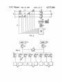
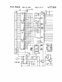
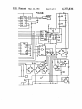
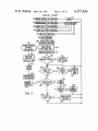
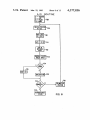
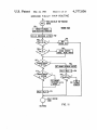
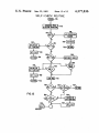
‘United States Patentv
[191
Elms et al.
[54] CIRCUIT INTERRUPTER WITH SOLID
STATE DIGITAL TRIP UNIT AND POSITIVE
POWER-UP FEATURE
[75] Inventors: Robert T. Elms, Monroeville; Gary F.
Saletta, Irwin; Bernard J. Mercier,
}
Appl. NOJ 140,632
'
Int. Cl.3 ............................................. .. H02H 3/ 10
US. Cl. ......................................... .. 361/96
[58]
Field of Search ............. ..
,
361/44, 92, 9,6, 98;
Shimp et al. .
'
Monitor.
Primary Examiner—Harry E. Moose, Jr.
Attorney, Agent, or Firm-Robert E. Converse, Jr.
[57]
U.S. PATENT DOCUMENTS
4,121,269 10/1978
“Results at Field Experiments of Digital Relays Utiliz
ing Minicomputer and Microprocessor”, Suzuki et al.,
“Operating and Instruction Guide”, Matco Energy
340/8702, 870.72, 870.24; 364/481, 492
References Cited
6/1974 Shimp .
7 England.
Power Systems, 6/ 1979.
[51]
[52]
5/1976
trol”—yHorne et a1; 1975 Conference Developments in
Power System Protection 11-13, Mar. 1975, London,
“Micro Versatrip Programmer . . . ”, Eckart Industrial
Apr. 15, 1980
3,818,275
Mar. 22, 1983
Bulletin, General Electric, 12/1978.
'
Filed:
3,956,670
[45]
tion of Electrical Power Systems, 2/1977.
“Motor Protective Relay IC305 MLTA”, Descriptive
[22]
[56]
4,377,836
IFAC Conference on Automatic Control and Protec
Pittsburgh, all of Pa.
[73] Assignee: Westinghouse Electric Corp.,
Pittsburgh, Pa.
[21]
[11]
.
Hobson, Jr. .......... ... ............ .. 361/44
4,232,236 11/1980 Yomogida et a1. ............. .. 361/92 X
OTHER PUBLICATIONS
“A Microprocessor Oriented Data Acquisition and
Control System for Power System Control”-Mulder,
3rd Annual Symposium on Computer Architecture,
Clearwater, Fla., 19-21, Jan. 1976.
‘
ABSTRACT .
A circuit interrupter includes a microcomputer con~
trolled trip unit having a front panel numeric display
and a plurality of LED displays for providing post
tripping indication of causeéof-trip and trip current
value. Reliable operation is provided during power up
conditions. Means are also provided for accurate per
formance of long delay and ground fault tripping opera
tion.
_
“Digital Processors for Substation Switching and Con
14 Claims, 14 Drawing Figures
791
I54,
ms? Y
u
szcmu
om nus n2
.
'
IIITERLOIX um
um um
2
or
module nmv:
"miss
a,’
mam
courum
01mm suasvs
11210 2.11210, 1c“
1m
rmmnm
Pom
fls
'92 cum 1
EH
‘Wit
FORTI
'57 PlO-Pl'!
AUTOMATIC’
mum:
n
IN
RESET
Pom
looI
I'UT SllSYSTEI
D/A
comm
U.S. Patent
Mar. 22, 1983
Sheet 1 of 13
4,377,836
U.S. Patent
Mar. 22, 1983
Sheet 2 of 13’
4,377,836
a
l:
av.“
DD
MANUAL
TRIP
colL’zz
TRIP’
,26
UNIT
FIG. 2
SOURCE l
-/56
SOURCE 2
58
FIG. 3
60) 1
1
1
@5
K
Q6
148
6/64
K
E: 66
,1
K
El '68
@
El/
EL/IZ
6
,U.S. Patent N Mar. 22, 1983
4,377,836
7 Sheet 3 of 13
$m28s;
\
3204
CURRENT
(IN NULTlPLESl 0F NAX. CONTINUOUS CURRENT)
FIG.4
US. Patent
Mar. 22, 1983
I54,
om aus m
SP
OTI
4,377,836
Sheet 4 of 13
IIITERLOOII AIIO
ARII or
v
on 0-1
LBACKPLAIIE DRIVE
IIICRO
ADDRESS
OOIIPUTER
OUTPUT SUBSYS
l/ZIO 2,IOIO, IOII
IO I
‘
EXTERNAL PROIA
om
‘I53
‘ PORT:l
ALU
RAN
IIIPUT SUBSYSTEII
COMPARATOR
I12 I62
REOTIFI
FEAR __1‘
UEIEUIUII
L PEAK
DETECTOR — RECTIFIER
gm
OROUNO CURRENT
FIG. 5
Patent
Mar. 22,1983
79
_ __L_ .
80
Sheet 5 of 13
‘
_
I
105
W? n
4,377,836
U.S. Patent
Mar.22, 1983
Sheet60f 13
moFLURTILP0"NWT
4,377,836 .
U.S. Patent
Mar. 22, 1983
.
Sheet 7 of 13
4,377,836
MAI N LOOP
‘2
6N
———————— -
F8 Mile
rn
om on RESE
“RESET
PUSH aunou
ClIAR TRIP
rs~ RESET PASE PEAK
nmcrmc CAPACITOR
“’
DELAY=I6.66T
,
—S0FTWARETIME
"0
COUNTERnOOUNTER-l ~ Fll
'
~ “
"52
mmcmou
DISPLAY
DISPLAY o 000
' TRIP VALUE
‘ ins
CLEAR
RAM
, ,rzo
DISCRIMINATORY]
TRIP ruucnou 7
COUNTER
COUNTER-l
1 -
m
FIG. 7
COUNTmZSSOR
1-4
F25,
LOAD
MINIMUM
ssn'mcs
‘
'U.S. Patent
Mar. 22, 1983
A/ D
Sheet 8 of 13
ROUTINE
3mm "r20
0-6» ,%
SET cam
PREVIOUS POSITION __
m A00.
smrr TEST ,
an mm
F29
m
SAVE IT IN R2
F3|
£21,120
VALUE
F32
COMPARE IT WITH ‘F33
ANALOG iNPUT
SAVE BT m as #56
F37
IS
OOIJNTER- I
F38
TRY NEXT BIT
POSITION
r59, Y
RETAINED VALUE
m A00.
FIG. 8
4,377,836
US. Patent _ Mar. 22, 1983
Sheet 9 of 13
4,377,836
SHORT DELAY ANDINSTATANEOUS TRIP ROUTINE
svmcn
m7 ‘m ms‘mmsous
PEAK nmcnns cmcunmr
}
00 All)
cowvgnslora F5‘
STORE PPC “F42
rm
TALLY- TALLY+|
r41
;
IS
PPOzITS
L
r44,
mm a
STORE VALUE
F46
‘
'
ls
TALLYzSD
TRIP &
STORE VALUE
'
T0 LONG DELAY TRIP FUNCTION
US. Patent
Mar.22, 1983
‘
LONG DELAY
Sheet 10 of 13
RIP ROUTINE
SWITCH 10 LD
.450
ACCURACY L0 - 32D
00 All)
,
CONVERSION F5‘
TALLY '
TALLY-MH
4,377,836
U.S. Patent
Mar. 22, 1983
Sheet 11 of 13
GROUND FAULT TRIP ROUTINE
' ma LUHG DELAY TRIP FUNCTIUH
wan
F6!)swncn T eaomw
@lm. 1LT
PEAK DETECTING GIRGUITRY
loo All) CONVERSION asroagi-rs2
SKIP
GROUND TEST
res,
GROUND CURREUTa
ACTUAL VALUE - PFC/4
4,377,836
US. Patent Mar. 22, 1983
Sh_eet12 of 13
4,377,836
SELF-CHECK ROUTINE -
@m
DlSGiARGE mu ,m'
omcnuc CAPACITOR
m '5 Y
"0'0
uocomaslon
‘
‘
FAILURE
II
"2)
Y
FAILURE on
us runcnon
I
‘
m
"hm
‘
n91 s51 rue
F80 nnuan
N
SET M;
I
F03
F85 ls
F84
res,
02 SD? Y
N
FAILURE
"8)0N
*
sm ruucnon
'
I"
,5 a1
N sunis 4 rss
\,
s51 FLAcvF89
mcnsum sun 45
Y
Y
“
\
(mumayrso
FIG. l2
FAILURE 0N
GFP FUNCTION
DELAY
DISPLAY i
;
U.S. Patent .’Mar.’22,198‘3 }
Sheet 13 of 13
_ 4,377,836
‘ ’ READT'ROM ROUTINE
H04 ,
VIRGIN PROM
' OR NO PROM IN SOCKET
LOAD MINIMUM SETTINGS
-
nos
I ADDRESS
montss,
+IOH mm
‘
[i
SET ERROR FLAGI
I
Fl06"( RETURN )
ADDRESS -l0II
I
READ NET 6 LOCTINS
FII2
Fus1
Y
I‘
‘
H LOAD mumuu
smmcs
LOAD smmcs m
CORRESPONDING RAN -/~Fl|4
LOCATION
(RETURNYHIS
FIG. l3
"1%
1
4,377,836
2
teristics were required such that a circuit breaker would
CIRCUIT INTERRUPTER WITH SOLID STATE
DIGITAL TRIP UNIT AND POSITIVE POWER-UP
FEATURE
rapidly open upon very high overload conditions but
would delay interruption upon detection of lower over
CROSS-REFERENCE TO RELATED
circuit breakers were called upon to interrupt upon the
APPLICATIONS
The present invention is related to material disclosed
in the following copending U.S. patent applications, all
load currents, the delay time being roughly inversely
proportional to the degree of overload. Additionally,
detection of ground fault currents. As the complexity of
electrical distribution systems increased, the control
portions of circuit breakers in a system were intercon
of which are assigned to the same assignee of the pres
nected to provide selectivity and coordination of inter
ruption sequences. This allowed the system designer to
specify the order in which the various circuit breakers
would interrupt under speci?ed fault conditions.
Engel;
During the late 1960’s solid-state electronic control
Ser. No. 140,631, “Circuit Interrupter With Front 15 circuits were developed for use in high power, low
Panel Numeric Display” ?led Apr. 15, 1980 by J. C.
voltage circuit breakers. These control circuits per
Engel, R. T. Elms, and G. F. Saletta;
formed functions such as instantaneous and delayed
Ser. No. 140,627, “Circuit Interrupter With Digital
tripping
which were traditionally achieved by magnetic
Trip Unit And Optically-Coupled Data Input/Output
and thermal means. The improved accuracy and ?exi
20
System” ?led Apr. 15, 1980 by J. C. Engel, J. A. Wafer,
bility of the solid state electronic controls resulted in
J. T. Wilson, and R. T. Elms;
their wide-spread acceptance, even though the elec
Ser. No. 140,554, “Circuit Interrupter With Energy
tronic control circuits were often more expensive than
Management Functions” ?led Apr. 15, 1980 by J. T.
their mechanical counterparts.
Wilson, J. A. Wafer, and J. C. Engel;
Ser. No. 140,628, “Circuit Interrupter With Digital 25 The earliest electronic control circuit designs utilized
discrete components such as transistors, resistors, and
Trip Unit And Style Designator Circuit” ?led Apr. 15,
capacitors. More recent designs have included inte
1980 by J. J. Matsko, E. W. Lange,‘ J. C. Engel, and B.
grated circuits which have provided improved product
J. Mercier;
performance at reduced cost.
Ser. No. 140,504, “Circuit Interrupter With Overtem
perature Trip Device” ?led Apr. 15, 1980 by J. J. Mat 30 As the cost of energy continues its rapid rise, there is
increasing interest in more effectively controlling the
sko, and J. A. Wafer;
usage of electrical energy through the design of more
Ser. No. 140,553, “Circuit Interrupter With Digital
Trip Unit and Means to Enter Trip Settings” ?led Apr.
sophisticated electrical distribution systems. Therefore,
15, 1980 by R. T. Elms, J. C. Engel, B. J. Mercier, G. F.
there is required a circuit breaker providing a more
35 complex analysis of electrical conditions on the circuit
Saletta, and J. T. Wilson;
Ser. No. 140,626, “Circuit Interrupter With Digital
being protected and even greater capability for coordi
Trip Unit And Power Supply” ?led Apr. 15, 1980 by J.
nation with other breakers. As always, it is extremely
C. Engel, J. A. Wafer, R. T. Elms, and G. F. Saletta;
desirable to provide this capability at the same or lower
Ser. No. 140,557, “Circuit Interrupter With Multiple
cost.
Display And Parameter Entry Means” ?led Apr. 15,
SUMMARY OF THE INVENTION
1980 by J. J. Matsko, J. A. Wafer, J. C. Engel, and B. J.
ent application.
Ser. No. 140,559, “Circuit Interrupter With Solid
State Digital Trip Unit” ?led Apr. 15, 1980 by J. C.
Mercier;
Circuit interrupter apparatus is provided for use on
Ser. No. 140,556, “Circuit Interrupter With Remote
an electrical power distribution system. The apparatus
Indicator And Power Supply” ?led Apr. 15, 1980 by J.
includes interrupter means for conducting current ?ow
C. Engel, J. A. Wafer, B. J. Mercier, and J. J. Matsko; 45 through an associated electrical circuit and for operat
Ser. No. 140,625, “Circuit Interrupter With ‘Digital
ing to interrupt current ?ow therethrough on com
Trip Unit And Automatic Reset” ?led Apr. 15, 1980 by
mand, means for sensing flow through the interrupter
B. J. Mercier and J. C. Engel; and
means, a digital processor, and a front panel display
Ser. No. 140,558, “Circuit Interrupter With Digital
system. The display system comprises a numeric display
Trip Unit And Potentiometers For Parameter Entry”
device and a plurality of electrically powered visual
?led Apr. 15, 1980 by J. C. Engel, B. J. Mercier, and R.
display indicators. Means are provided to prevent nui
sance tripping upon system power-up, to determine
BACKGROUND OF THE INVENTION
peak current values for each cycle of AC current, and
to
insure the most conservative settings if unreliable
1. Field of the Invention
55
values of time-current tripping characteristic parame
The invention relates to circuit interrupters having
ters are entered. Cause of trip and display of trip current
means for electronically analyzing the electrical condi
is also provided. Accurate determination of long delay
tions on the circuit being protected, and means for auto
T. Elms.
matically opening to interrupt the current flow when
, ever electrical conditions exceed predetermined limits. 60
2. Description of the Prior Art
Circuit breakers are widely used in industrial and
_ commercial applications for protecting electrical con
ductors and apparatus connected thereto from damage
and ground fault trip operation is also provided.
BRIEF DESCRIPTION OF THE DRAWINGS
FIG. 1 is a perspective view of a circuit breaker em
bodying the principles of the present invention;
FIG. 2 is a functional block diagram of the circuit
due to excessive current flow. Circuit breakers were 65 breaker shown in FIG. 1;
initially designed to interrupt when the current ?owing
FIG. 3 is an electrical schematic diagram of a distri
through them exceeded a certain level. Gradually, how
ever, more elaborate time-current interrupting charac
bution system employing the circuit breaker of FIGS. 1
and 2;
3
4,377,836
FIG. 4 is a graph of a typical time-current tripping
characteristic, plotted on a log-log scale;
FIG. 5 is a block diagram of the trip unit shown in
FIGS. 1 and 2;
FIGS. 6A and 6B are partial schematic diagrams of 5
the trip unit circuitry of FIG. 5;
4
operator to manually charge a spring (not shown) in the
mechanism 20. The manual controls 32 are positioned in
the center of the housing 34. Windows 38 and 40 indi
cate the state of charge of the spring and the position of
the contacts 18, respectively. A push-button 42 allows
an operator to cause an internal electric motor to me
FIG. 7 is a general ?ow chart of the program stored
chanically charge the spring in the same manner as the
manual charging operation which can be performed by .
FIG. 8 is a flow chart of the analog-to-digital routine
the handle 36. A pushbutton 44 allows an operator to
stored in the memory of a microcomputer which is a 10
cause the spring to operate the mechanism 20 to close
component of the trip unit;
the contacts‘ 18. Similarly, a pushbutton 46 allows an
FIG. 9 is a ?ow chart of the short delay trip and
operator to cause the spring and mechanism 20 to open
in the memory of the microcomputer;
instantaneous trip functions of the program of FIG. 7;
FIG. 10 is a ?ow chart of the long delay trip function
the contacts 18.
'
The panel of the trip unit 26 is positioned on the left
of the program of FIG. 7;
15 side of the housing 34 as can be seen in FIG. 1. This
FIG. 11 is a ?ow chart of the ground trip function of
panel includes a numeric display device 80 to permit an
the program of FIG. 7;
operator to observe the value of electrical parameters
FIG. 12 is a flow chart of the self-checking routine of
on the circuit being protected, a plurality of light-emit~
the program of FIG. 7; and
FIG. 13 is a ?ow chart of the routine to read external 20 ting diode (LED) indicators 84, 86, and 88, a rating plug
78 to determine the maximum continuous current of the
breaker, and a plug-in programmable read-only mem
FIG. 8.
programmable read-only-memory of the program of
ory (PROM) chip 82 to de?ne the time-current trip
characteristic of the breaker.
DESCRIPTION OF THE PREFERRED
EMBODIMENT
25
General Physical and Electrical Description
Reference may now be had to the drawings, in which
like reference characters refer to corresponding compo
_ nents. A perspective view and a functional block dia
USE OF A CIRCUIT BREAKER IN AN
ELECTRICAL POWER DISTRIBUTION SYSTEM
Before explaining the operation of the trip unit, it will
be helpful to describe in greater detail the function of a
gram of a moled case circuit breaker l0 employing the 30 circuit breaker in an electrical power distribution cir
principles of the present invention are provided in
FIGS. 1 and 2, respectively. Although the circuit inter
cuit. FIG. 3 shows a typical electrical distribution sys
tem. A plurality of electrical loads 48 are supplied
rupter 10 is a three-pole circuit breaker for use on a
through circuit breakers 50, 52 and 54 from either of
three-phase electrical circuit, the invention is, of course,
two sources of electrical energy 56 and 58. The sources
not so limited and could be used on a single-phase cir 35 56 and 58 could be transformers connected to separate
high voltage electrical feeder lines, diesel-powered gen
cuit or another type of multiphase circuit.
erators, or a combination of the two. Power from the
A power source such as a transformer or switchboard
first source 56 is supplied through the ?rst main circuit
bus is connected to input terminals 12 and an electrical
breaker 50 to a plurality of branch circuit breakers 60,
load is connected to output terminals 14. Internal con
ductors 16 connected to the terminals 12 and 14 are also 40 62, 64, and 66. Similarly, power from the second source
58 may be supplied through the second main circuit
connected to interrupting contacts 18 which serve to
breaker 52 to a second plurality of branch circuit break
selectively open and close an electrical circuit through
ers 68, 70, 72, and 74. Alternatively, power from either
the circuit breaker. The contacts 18 are operated by a
source 56 or 58 may be supplied through the tie circuit
mechanism 20 which responds to manually or automati
cally-initiated commands to open or close the contacts 45 breaker 54 to the branch circuit breakers on the oppo
18.
\
site side. Generally, the main and tie circuit breakers 50,
Current transformers 24 surround each of the internal
phase conductors 16 to sense the level of current flow
through the conductors 16. The output from the current
simultaneously supplied by both sources. The capacity
the level of ground fault current flowing in the circuit.
The trip unit 26 constantly monitors the level of phase
and ground fault currents ?owing in the circuit to
occur at, for example, the point 76, it is desirable that
this condition be detected by the branch circuit breaker
52 and 54 are coordinated so that no branch circuit is
of the main and tie circuit breakers 50, 52 and 54 is
transformers 24 is supplied to a trip unit 26, along with 50 usually greater than that of any branch circuit breaker.
the output from a current transformer 28 which senses
If a fault (abnormally large current ?ow) should
62 and that this breaker rapidly trip, or open, to isolate
which the breaker 10 is connected and initiates a com 55 the fault from any source of electrical power. The fault
mand signal to a trip coil 22 which actuates the mecha
at the point 76 may be a large over-current condition
nism 20 to open the contacts 18 whenever electrical
caused, for example, by a short circuit between two of
conditions on the circuit being protected exceed prede
termined limits stored in the trip unit 26. During normal
the phase conductors of the circuit, or an overload only
slightly above the rating of the breaker such as might be
conditions, the mechanism 20 can be commanded to
caused by an overloaded motor. Alternatively, it may
open and close the contacts 18 through manually
be a ground fault caused by a breakdown of insulation
initiated commands applied through the manual con
on one of the conductors, allowing a relatively small
trols 32.
amount of current flow to an object at ground potential.
Referring to FIG. 1, it can be seen that the circuit
In any case, the fault would also be detected by the
breaker 10 includes a molded insulating housing 34. The 65 main or tie breakers 50, 52 or 54 through which the load
terminals 12 and 14 are on the rear of the housing 34 and
fed by branch breaker 62 is supplied at the time of the
are thus not shown in FIG. 1. A handle 36 is mounted
fault. However, it is desirable that only the branch cir
on the right-hand side of the housing 34 to allow an
cuit breaker 62 operate to isolate the fault from the
5
4,377,836
source of electrical power; The reason for this is that if
- the main or tie circuitvbreakerv should trip, electrical
power would be lost to a greater portion of the entire
system than merely the load attached to the branch
circuit on which the fault occurred. It is therefore desir
able that the main' and tie circuit breakers 50, 52 and 54
should have a longer delay period following detection
of a fault before they initiate a tripping operation. The
coordination of delay times among the main, tie, and
branch circuit breakers for various types of faults and
the need for interlocking between breakers are major
reasons for the need to provide sophisticated control in
a trip unit.
TIME-CURRENT TRIPPING
CHARACTERISTICS
In order to achieve the coordination between circuit
breakers as described above, the time vs. current trip
ping characteristics of each circuit breaker must be
6
TRIP UNIT FUNCTIONS AND MODES
The functions and modes of the trip unit 26 employ
ing the principles of the present invention will now be
described. A rating plug 78 is inserted into the front
panel of the trip unit 26 to specify the maximum contin
uous current to be allowed in the circuit being protected
by the circuit breaker. This may be less than the actual
capacity of the circuit breaker, which is known as the
frame size. For example, the frame size for the circuit
breaker may be 1,600 amperes; however, when the
breaker is initially installed the conductors of the circuit
being protected may be sized so as to continuously
supply only 1,200 amperes of electrical current. There
fore, a rating plug can be inserted in the trip unit to
ensure that the maximum continuous current allowed
by the circuit breaker will be only 1,200 amperes even
though the circuit breaker itself is capable of safely
carrying 1,600 amperes continuously.
speci?ed. Circuit breakers have traditionally exhibited
Throughout the remainder of the description of the
characteristics similar to that shown in FIG. 4, where
invention, current levels may be described as multiples
both axes are plotted on a logarithmic scale. When
of the maximum continuous current as speci?ed by the
rating plug. This convention will be expressed as, for
current below the maximum continuous current rating
of the breaker is ?owing, the breaker will, of course,
remain closed. As current increases, however, it is de
sirable that at some point, for example the point 300 of
FIG. 4, the breaker should trip if this overload current
persists for an extended period of time. Should a current
?ow equal to the maximum continuous current rating as
speci?ed by‘point 300 persist, it can be seen from FIG.
4 that the breaker will trip in approximately 60 seconds.
At slightly higher values of current, the time required
for the breaker to trip will be shorter. For example at
. 1.6 times maximum continuous current as speci?ed by
example, 3 per unit or 3 p.u. to indicate a current level
of three times the maximum continuous current.
As can be seen in FIG. 1, the trip unit panel contains
a numeric display indicator 80 and a number of LED
indicators 84, 86, and 88. The electronic circuitry inter
nal to the trip unit causes the numeric display indicator
80 to sequentially display the present value of electrical
conditions on the circuit being protected and the vari
ous limit settings de?ning the time-current trip curve of
the breaker as currently set. The LED’s 84, 86 and 88
indicate whether a ground fault, long delay overcur
point 302, the breaker will trip in about 20 seconds. The
portion of the curve between the points 300 and 304 is
known as the long delay, or thermal, characteristic of
the breaker, since this characteristic was provided by a
To the right and below the numeric display indicator
80 and rating plug 78 is a plug-in programmable read
bimetal element in traditional breakers. It is desirable
that both the current level at which the long delay
only memory (PROM) module 82, such as a type 3601
manufactured by the Intel Corporation, in which are
portion begins and the trip time required for any point
stored the various limit values and settings which spec
ify the time-current tripping characteristics of this par
ticular circuit breaker. The method of loading the set
tings into ‘this module and the manner in which the
module is used by the trip unit circuitry will be de
on that portion be adjustable. These parameters are
known as long delay pick-up and long delay time, re
spectively, the variation of which is indicated by the
arrows 306 and 308.
At very high overcurrent levels, for example 12 times
the maximum continuous current and above, it is desir
able that the circuit breaker trip as rapidly as possible.
This point 312 on the curve is known as the “instanta
rent, or “instantaneous” overcurrent was the cause of a
trip operation.
scribed in a later section.
SYSTEM DESCRIPTION
The trip unit circuitry includes a digital arithmetic
neous” or magnetic, trip level, since traditional breakers
logic and control processor 154 such as the type 8048
employed an electromagnet in series with the contacts
to provide the 'most rapid response. The instantaneous
microcomputer manufactured by the Intel Corporation,
pick-up level is usually adjustable, as indicated by the
and is presented by block diagram in FIG. 5. This sec
tion will describe each block of FIG. 5 and present a
arrow 314.
description of the operation of the trip unit.
To aid in coordinating breakers within a distribution
system, modern circuit breakers have added a short
The microcomputer 154 contains an arithmetic logic
unit (ALU) 153, 64><8~bit bytes of read-write random
access memory (RAM) 155, 1KX8-bit bytes of read
only memory (ROM) 157, an 8-line data bus 172, and
‘delay trip characteristic 316 between the long delay and
instantaneous portions. The present invention allows
adjustment of both the short delay pick-up level and the
short delay trip time as indicated by the arrows 318 and
v 320.
_ two 8-line input-output ports Port 1 and Port 2. Other
types of digital arithmetic logic and control processors
could be used, such as those requiring outboard mem
Under certain conditions it is desirable that the trip
ory circuits rather than having the on-chip RAM and
time over the short delay portion vary inversely with 65 ROM circuits of the 8048. However, for a detailed
the square of the current. This is known as an I2t char
description of the microcomputer, reference should be
acteristic and is indicated in FIG. 4 by the broken line
made to the MCS-48 Microcomputer User’s Manual
310.
published by the Intel Corporation.
7
4,377,836
8
crocomputer 154. The technique is shown in greater
detail in the ?ow chart of FIG. 8.
The function of transistors 102 and 104 and their
CIRCUIT DESCRIPTION
Referring to‘ the system block diagram of FIG. 5 and
the detailed schematic diagrams of FIGS. 6A and 6B,
the display section 79 is ?rst described. It consists of
four data latches IC5, 1C6, 1C7 and 1C8 and the four
associated components is to direct the phase (or ground)
currents from the CTS 24 and 28 to the rating plug
resistor 105 during non-tripping operation. However,
digit liquid crystal numeric display 80. The data latches
when a trip condition is sensed and the trip SCR 98 is
may be the type MC 14543. Display data is multiplexed
on the data bus 172 of the microcomputer; the four least
signi?cant bits represent data and the four most signi?
cant bits its position on the display. The liquid crystal
display 80 derives its back plane clock from the interval
turned on, transistors 102 and 104 are turned off,
thereby directing essentially all of the phase (or ground)
current signal into the shunt trip coil for a positive
tripping action.
Power for the trip unit circuitry is supplied by re
timer 92. This interval timer also ful?lls the function of
chargeable battery with charging power produced by
resetting the microcomputer if it does not receive its
clock signals from the microcomputer 154. Under nor
mal operation, the microprocessor outputs a pulse on
every execution of the main program loop.
the current transformers 24. Alternately, power could
be derived directly from the current transformers 24 or
independently via connections to the conductors 16.
outputs its contents via Port 1. Since the display section
DESCRIPTION OF OPERATION
The operation of the invention is described in detail in
this section. In the ?rst part, a general ?ow chart of the
79 and the address lines of the PROM 82 are both con
program and the allocation of memory are presented.
nected to the data bus 172, the address information for
the PROM would tend to cause a garbled display. How
ever, the address information appears on the bus for
only a small fraction of a second, to be immediately
be described in the second part.
It can be seen on the diagram of FIG. 5, that the
PROM 82 receives its address from the data bus 172 and
Major subroutines called from the main loop will then
DATA MEMORY ALLOCATION
The allocation of the internal RAM 155 of the mi
crocomputer 154 is shown in Table I.
TABLE I
followed by valid display information. The LCD dis
play therefore does not have time to respond to the
PROM address information and the operator observes
only the valid display information.
The output subsystem 94 consists of % of a type A775
comparator 1C2, and of quad NOR gate IC10 and quad
NAND gate IC11. Through comparator 1C2 the mi
30
DATA MEMORY MAP (RAM)
63
62
61
Long Delay Pick-up (LDP)
Long Delay Time (LDT)
Short Delay Pick-up (SDP)
signal after a ground fault pickup. Through the NAND 35
60
Short Time (SDT)
gate of IC11 the microcomputer sets the corresponding
59
58
Instantaneous Trip Setting (ITS)
Ground Fault Pick-up (OFF)
LED indicator 84, 86 or 88 after a trip.
57
Ground Fault Time (GFT)
crocomputer 154 via Port 2 sets an interlock output
The NOR gates IC10 provide the high-level output
signal to trip a single SCR 98 under ground, short delay,
long delay, or instantaneous trip. It also forces this trip
signal to follow the RESET signal during power-up
thus eliminating false tripping during the 10 ms period
of microcomputer instability after power is ?rst applied.
The input subsystem 100 consists of two peak detect
ing circuits including capacitors 90 and 91, a type
ZN425J D/A converter 1C4, the other half of compara
tor 1C2, and the analog switches of 1C3. The capacitors
90 and 91 store the peak value of phase and ground
current, respectively, for each cycle of the AC line. The
peak values are then read every cycle by the microcom
puter. The capacitors 90 and 91 are reset (discharged)
later in each cycle by the microcomputer through a
,transistor 96 and IC11 activated by Port 2.
The analog-to-digital conversion of the signal from
the input subsystem 100 is accomplished by an iteration
technique employing the D/A converter 1C4 and com
parator 1C2. A digital value is supplied to the D/A
converter 101 by the microcomputer 154. This value is
converted to an analog value and supplied to 1C2. 1C2
then compares this value to the value supplied from
capacitors 90 or 91 through the analog switch 1C3 and
indicates whether or not the value supplied by IC4 is
larger. The result of this comparison is supplied via the
T1 test input to the microcomputer 154, which then
40
45
56
55
54
53
52
51
Sum
Sum
Sum
Sum
6 = Tally of GFT
4 = Tally of SDT
45 = Self-checking Sum 4
65 = Self-checking Sum 45
5O
49
48
47
46
45
Sum 3 = Lower Tally of LDT
Sum 2 = Middle Tally of LDT
44
43
42
Sum l = Upper Tally of LDT
41
Trip Flag
40
Cycle Counter
39
38
37
Present value of inst. current
Present value of GND current
36
Trip value
35
55
34
33
32
Display index
Low byte of addr. of next display
High byte of addr. of next display
As can be seen, the top eight locations are used to
load the limit value settings, such as Long Delay Pick—
Up and Long Delay Time. The values in these locations
are refreshed every 4 seconds, after a reading of the
external PROM 82. The tallies for ground fault, short
delay, and long delay timing functions are also kept in
generates a new value to 1C4. This process continues 65 RAM. The address of the next information to be dis
until the value generated by the microcomputer 154 is
very close to that supplied by the analog switch 1C3,
and the result is retained in the accumulator of mi
played, the present value of ground and instantaneous
current, and the trip value are stored in locations
shown. The addressing of those values is done indi
9
4,377,836
rectly through Register (0 (R0) or Register 1 (R1) which
contains the particular address.
The lower 32 words of data memory are used for
standard “housekeeping” functions of the microcom
puter, as explained in the previously referenced Intel
unit format, the parameter being displayed is identi?ed
by a numeric code which appears ‘concurrently with the
parameter value in the left-most digit of the numeric
display 80, as follows:
1. Present Phase Current
User’s Manual.
MAIN LOOP
Refer to the flow chart of the main loop shown in
FIG. 7. After the system is powered-up or the reset
button on the front panel is pushed, the program
counter of the microcomputer 154 is loaded automati
cally with 00¢ hex. An instruction at this location
brings the microcomputer to three initialization rou
tines: clear RAM, load display with M010, and perform
discriminatary trip function. In the latter function, the
10
tion is done immediately after reading the PROM 82
and 255 X16667 ms (4.27 sec) thereafter.
The parameter display is a three-digit number in per
2. Long Delay Pick Up
. Long Delay Time
. Short Delay Pick Upv
. Short Delay Time
. Ground Fault Pick Up
. Ground Fault Time
15
. Instantaneous Trip Level
. Present Ground Current
present value of the phase current is compared with 9.0
When the counter reaches 125 (2.1 sec) and if an error
p.u., i.e. nine times rated current. Thus, if the breaker is
was found in the self-checking routine, an error code
experiencing a high overload when the trip unit is ?rst
will be displayed in the indicator 80 instead of a parame
powered-up, the program is able to trip the breaker 20
ter value: 1 for A/D conversion failure or instantaneous
within 0.5 ms. These initialization routines are executed
trip function failure, 2 for short delay function failure, 3
only during power-up or reset.
for. ground trip function failure, and 4 to indicate that
At this point the program counter is decremented to
minimum
settings are being used.'This will cause the
FF hex or 255 decimal. This count signals the mi
crocomputer 154 to read the external PROM 82. If the 25 indicator 80 to change from parameter value to error
code every two seconds, indicating to the user that an
PROM 82 is unreadable (contents= MH or FFH) or the
error was found.
checksum is invalid, minimum limit value settings (from
ROM 157 internal to the microcomputer) are loaded in
DETAILED DESCRIPTION OF OPERATION
This section will describe, in detail, the function
corresponding RAM locations. Otherwise, the last six
teen memory locations of the PROM 82 are read. The 30
blocks shown in the general flow diagram. Reference
use of a 2K PROM will thus allow the user to repro
should be made to the ?ow diagrams presented for each
gram a new set of limit values into the PROM 16 times,
block.
before a new PROM must be employed. (16x16 va
GIN. From then on, this will be the starting point of the
Considering the instantaneous trip function and short
delay trip function ?rst, refer to the flow chart of FIG.
9. Upon entering those two routines, the microcom
main loop.
puter 154 switches the D/A converter IC4 analog out
The internal ROM 157 of the microcomputer 154
includes a look-up table containing the addresses of the
tors 108, 110 and 112, having values of 6.8K, 220K, and
lues><8 bits per value=2048). After reading values
from PROM, the program jumps to entry location BE
35
put to the phase peak detecting circuitry through resis
subroutines which prepare the formats to enable the 40 220K, respectively. This produces a scale factor of l
p.u. (with a digital representation of 160). The A/D
various parameter values to be displayed. Through an
conversion (FIG. 8) subroutine is now called which
index R34 (initialized at 0) and updated by each display
‘lasts 0.26 ms (104 instructionsX2.5 ucs average execu
routine) the address of the next display routine is read
tion time).
and stored in R33 and R32 of RAM 155.
The A/D conversion subroutine operates by clearing
Next, the four main functions of the program are 45
the accumulator, then setting the most signi?cant bit
entered: the instantaneous trip function, the short delay
trip function, the long delay trip function and the
ground trip function. Those functions will be presented
in detail in the next section.
A self-checking subroutine is next executed. In this 50
subroutine, the analog-to-digital converter, short delay
pick-up, and ground test functions are checked. If a
failure is detected, a failure flag is set and an error code
stored in RAM 155.
thereof as a test value. This value is sent to the D/A
converter which produces a corresponding analog
value. This analog value is compared to the phase cur
rent value provided by the peak detecting capacitor 90.
If the trial analog value is smaller than the phase cur
rent, then the trial value consisting of one bit is added to
the digital successive approximation of the phase cur
rent value which is retained in register R3. The test bit
The capacitors 90 and 91 for storing peak phase and 55 in the accumulator is then shifted one place to the right,
a corresponding analog test value generated, a compari
ground current are then discharged and a time delay
son made, and the bit is retained or not in register R3
executed equal to 16.667 ms less the time expended in
executing the main loop instructions.
according to the results of the comparison. In a similar
A ?ag is next checked to determine if a tripping oper
manner all eight bits of the accumulator are tested and
ation has occurred. If so, the value of phase or ground
at the completion of the eighth bit, the retained value in
current which caused the trip is now displayed. Since
R3 is transferred to the accumulator.
the trip unit is powered externally, a tripping operation
’ will not inhibit execution of the microcomputer soft
ware.
The digital value of present phase current (PPC) is
then stored in RAM 155 in order to be displayed and
used in the Short Delay routine. If PPC is greater than
After the ?rst cycle, the main counter is ‘at 254D. This 65 the instantaneous trip setting (ITS), a tripping operation
number signals the microcomputer 154 to select another
parameter to be displayed by the indicator 80. Realizing
that this count is circular, it can be seen that the selec
is executed, which includes the function of saving the
current value which caused the trip (to be displayed on
indicator 80) and lighting the proper LED 84, 86 or 88
4,377,836
.
12
11
to indicate cause-of-trip. Otherwise, the short delay trip
frame rating, the ground fault pick-up is desensitized so
function is entered.
that the fictitious ground fault current (an artifact of the '
current transformers) will not cause an improper trip, In
the present trip unit as can be seen in the ?ow chart of
‘
In the Short Delay routine, a tally is incremented'
every cycle if the PPC is larger than the short delay
pickup. The tally is then compared to a value corre
FIG. 11, further corrective action is provided. The
ground fault pick-up is desensitized, as in the prior art,
when PPC is greater than or equal to 7.0 PU; however,
sponding to the short delay time setting (SDT). If the
tally is greater than the SDT value, a trip operation is
called for. Otherwise, the Long Delay Test routine is
for PPC between 1.0 and 7.0 PU, the ?ctitious ground '
entered. If the PPC is smaller than’ the short delay
pickup the short delay tally is reset to zero. At this point O current is accounted for by subtracting from the ground
current sensed, the PPC divided by 4. This method
the Long Delay Test (LDTST), as shown in FIG. 10, is
could, of course, be accomplished by other means, such
entered.
Upon entry, the LDTST function switches (through
1C3) to the phase peak detecting circuitry. However,
as analog circuitry.
ground current pick-up setting, the ground interlock
this is done through resistors 114 and 116 having values
of 3.3K and 220K, respectively (see FIG. 6). Thus, the
output is set, to signal other breakers that this breaker is
monitoring of a ground fault. Next a tally similar to the
short delay tally is incremented. If this tally is now
threshold level in the A/D conversion process is dou
bled. Keeping in mind that 1 p.u. was encoded as 16D in
the instantaneous trip and short delay functions, it can
be seen that now 1 p.u. is encoded as 32D (a resolution
of 3.12%).
For long delay timing a quantity proportional to (i)2
20
must be calculated. This value is added to an accumulat
ing register and then compared to the Long Delay Time
(LDT) setting whenever the Long Delay Pick-up
(LDPU) setting is exceeded. The accumulating register
25
greater than the ground fault tally trip value, a trip
operation is performed. Otherwise, the program enters
the self-checking routine.
If the present ground current is less than the ground
current pick-up setting, but greater than 1 the setting,
the ground interlock output is set. In addition, for all
values of ground current less than the setting, the tally
is decremented (not reset as in Short Delay) and the
then represents “(i)2t”. The use of an example will illus
trate the procedure used:
_
If the ‘present ground current is greater than the
self-checking routine is entered.
‘
Suppose
Refer to the self-checking routine in FIG. 12. This
routine, performed every cycle, resets the peakdetect
30 ing capacitors 90 and 91 and checks the running tally of
ground fault and short delay functions, alerting the user
to a malfunction of the main loop. This is done by set
ting ?ags which are checked every 2.1 seconds in the
main loop, and storing an error code. If the ?ag is set,
35 the main loop causes an error code number to appear on
the numeric display 80. Thus, instead of a four-second
display of parameter values, there would be alternate
Instead of storing i2, however, the quantity i2/4 is
2.1 second displays of error codes and parameter values.
As stated previously, the READ routine shown in
retained since less memory space is required, and suffi
cient resolution still maintained. Thus:
FIG. 13 allows the user to reprogram the external
PROM chip with new set point limit values up to 16
i2/4=36,864/4=9216.
times via a PROM programmer. It also loads minimum
settings for the breaker, if the PROM was not correctly
If i2/4 is accumulated into a tally of 24 bits every l/ 60
programmed or the PROM is missing.
45
of a second, in two seconds the tally will be:
As an example, the settings may be encoded in
PROM 82 as follows:
92l6><60><2=l,105,920D
which brings the upper eight bits of the tally to the
EXAMPLE
value:
(X 32) LDPU of.8 PU = 8 X 32
= 26 D
= 1A H
R
1,105,920
(X 8.5) LDT ofZ sec
(X 16)SDPU of 1.5 PU
(X l) SDT of 20 cycles
(X 64) GFP of .2 PU
(X 1) GFT of 20 cycles
(X 16)ITC of 8.0 PU
: 17D
216
Thus, an LDT setting for 2 seconds, encoded as 17 D or
11 H, is reached in exactly 2 seconds as desired. There
fore, LDT setting=# of seconds>< 17/2. It must be
realized that with lower PPC the trip unit will take
longer time to reach that count, and with larger PPC
the trip unit will reach that count faster (time will be
inversely related to (i)2).
Referring to the ?ow chart of FIG. 10, it can be seen
that when the PPC is less than LDPU the tally is decre
=
=
2 X 8.5
1.5 X 16
=
=
=
=
=
=
20 X 1
.2 X 64
20 X 1
8 X 16
=
=
=
=
17 D
24 D
20 D
12.8 D
20 D
128 D
=
=
11H
18 H
= 14 H
= OD H
= 14 H
= 80 H
55
In this format the settings are ready to be used by the
program. However, in order to be displayed‘ (every 4
seconds) they must be each converted to recognizable
decimal characters.
Thus, every display routine calls a routine to convert
the integer and fraction portions of the display value
mented with a ?xed value of A4 H: 164 D. This num
from hex format to BCD. The BCD values are then
ber represents the (LDP min)2/4 or (0.8X 32
D)2/4= 164 D.
converted to 7-segment format by the latch decoders.
The ground fault test function is now performed. In
prior art trip units, on non-ground faults in which the
phase current is between three and ten times the breaker
What we claim is:
1. Circuit interrupter apparatus, comprising:
interrupter means for conducting alternating current
flow through a circuit to be protected and for oper