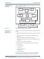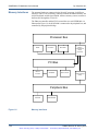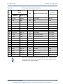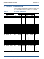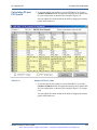
1
Artisan Technology Group is your source for quality
new and certified-used/pre-owned equipment
• FAST SHIPPING AND
DELIVERY
• TENS OF THOUSANDS OF
IN-STOCK ITEMS
• EQUIPMENT DEMOS
• HUNDREDS OF
MANUFACTURERS
SUPPORTED
• LEASING/MONTHLY
RENTALS
• ITAR CERTIFIED
SECURE ASSET SOLUTIONS
SERVICE CENTER REPAIRS
Experienced engineers and technicians on staff
at our full-service, in-house repair center
WE BUY USED EQUIPMENT
Sell your excess, underutilized, and idle used equipment
We also offer credit for buy-backs and trade-ins
www.artisantg.com/WeBuyEquipment
InstraView REMOTE INSPECTION
LOOKING FOR MORE INFORMATION?
Visit us on the web at www.artisantg.com for more
information on price quotations, drivers, technical
specifications, manuals, and documentation
SM
Remotely inspect equipment before purchasing with
our interactive website at www.instraview.com
Contact us: (888) 88-SOURCE | [email protected] | www.artisantg.com
Document Number: 809606
Revision: D
Date: January 2003
SVME/DMV-179
Hardware User’s Manual
DY 4 Systems Inc.
333 Palladium Drive
Kanata, Ontario, Canada
K2V 1A6
(613) 599-9199
Artisan Technology Group - Quality Instrumentation ... Guaranteed | (888) 88-SOURCE | www.artisantg.com
SVME/DMV-179 Hardware User’s Manual
Dy 4 Systems Inc.
Revision History
ii
Rev
By
Date
Description
-
BJ
December 1999
First release. This document is associated with SVME/DMV-179 products manufactured using PWB # 310939-003 or later.
A
BJ
July 2000
Removed the BI-mode section from Chapter 1 as BI-mode is no longer supported.
Added “Cache Coherency” on page 1-29.
Added note to “EIA-422/485 Interface” on page 1-36.
Corrected Bridge Timer information in Table 1.6 on page 1-45.
Corrected Watchdog information on page 1-46.
Corrected diagram of J9 connector (Figure 2.3 on page 2-27).
Corrected Table 2.1 on page 2-3.
Corrected Table 2.15 on page 2-18 and Table 2.18 on page 2-23.
Improved page 3-4.
Corrected Figure 3.1 on page 3-31.
Corrected “VMEbus Base Addresses” on page 3-34.
B
BJ
June 2001
Modified “Serial EEPROM” on page 1-31.
Modified “Reset” on page 1-33.
Corrected “SCSI I/O Pinout” on page 1-39.
Modified “Watchdog Timer” on page 1-46.
Modified “Reset Supervisor” on page 1-48.
Added “Using the SVME/DMV-179 Pinout Configurator” on page 2-44.
Changed references to “Parallel I/O” to “Discrete Digital I/O” in Chapter 3.
C
BJ
February 2002
Updated to reflect PWB 310939-004. This PWB has a jumper (E48 - E49) for
selection of the Permanent Alternate Boot Site.
Added mention of E48 - E49 to “Permanent Alternate Boot Site” on page 1-30.
Added mention of E48 - E49 to “Non-Volatile Memory Map” on page 1-31.
Updated “JTAG” on page 1-34.
Updated “Real Time Clock (RTC)” on page 1-41.
Improved “RTC Power Supply” on page 1-42.
Corrected Real Time Clock entry in Table 1.6 on page 1-45.
Improved “Discrete Digital I/O” on page 1-49.
Added notes about EIA signal naming conventions on page 2-6 and on page
2-19.
Corrected Table 2.8 on page 2-11.
P1-A16 is DTACK* in Table 2.9 on page 2-12 and Table 2.11 on page 2-14.
Updated Table 3.8 on page 3-12.
Corrected Table 3.10 on page 3-14.
Corrected Figure 3.1 on page 3-31.
Added note below Figure 3.1 on page 3-31.
Corrected “GT-64130” on page 3-32.
Corrected A24 addresses in Table 3.30 on page 3-34.
D
BJ
January 2003
Updated “64-bit Flash Protection” on page 1-30.
Updated “Serial EEPROM” on page 1-31.
Updated “EIA-422/485 Interface” on page 1-36.
Updated Table 1.6 on page 1-45.
Updated “Discrete Digital I/O” on page 1-49.
Throughout Chapter 2, SCSI signals now have a “*” to indicate they are active
low.
Corrected Table 3.11 on page 3-15.
809606 Revision D January 2003
Artisan Technology Group - Quality Instrumentation ... Guaranteed | (888) 88-SOURCE | www.artisantg.com
Dy 4 Systems Inc.
Copyright Notice
The information in this document is subject to change without notice and
should not be construed as a commitment by Dy 4 Systems Inc. While
reasonable precautions have been taken, Dy 4 Systems Inc. assumes no
responsibility for any errors that may appear in this document.
No part of this document may be copied or reproduced without the prior
written consent of Dy 4 Systems Inc.
The proprietary information contained in this document must not be disclosed
to others for any purpose, nor used for manufacturing purposes, without
written permission of Dy 4 Systems Inc. The acceptance of this document will
be construed as an acceptance of the foregoing condition.
Copyright © 2003, Dy 4 Systems Inc. All rights reserved.
Trademarks
AltiVec is a trademark of Motorola, Inc.
BI-mode is a registered trademark of Dy 4 Systems Inc.
DiskOnChip is a registered trademark of M-Systems Inc.
Dy 4 COTS is a trademark of Dy 4 Systems Inc.
Ethernet is a trademark of Xerox Corporation.
LynxOS is a trademark of Lynx Real-Time Systems, Inc.
PowerPC is a trademark of International Business Machines Corporation.
Tornado and Wind River are trademarks and VxWorks is a registered
trademark of Wind River Systems, Inc.
Universe II is a trademark of Tundra Semiconductor Corporation.
UNIX is a registered trademark in the U.S. and other countries, exclusively
licensed through X / Open Company, Ltd.
All other brand and product names are trademarks or registered trademarks of
their respective owners.
809606 Revision D January 2003
Artisan Technology Group - Quality Instrumentation ... Guaranteed | (888) 88-SOURCE | www.artisantg.com
iii
SVME/DMV-179 Hardware User’s Manual
iv
Dy 4 Systems Inc.
809606 Revision D January 2003
Artisan Technology Group - Quality Instrumentation ... Guaranteed | (888) 88-SOURCE | www.artisantg.com
Dy 4 Systems Inc.
Table of Contents
Table of Contents
Preface........................................................................................................................................................ xiii
Purpose ................................................................................................................................................ xiii
Audience.............................................................................................................................................. xiii
Scope ................................................................................................................................................... xiii
Reference Documents.......................................................................................................................... xiii
1. Functional Description................................................................................................1-1
SVME/DMV-179 Architecture.................................................................................................................. 1-3
SVME/DMV-179 Features List ................................................................................................................. 1-5
Central Processing Unit (CPU) .................................................................................................................. 1-6
PowerPC 7400 and 750 Architecture .................................................................................................. 1-6
PowerPC 7400 Features....................................................................................................................... 1-7
PowerPC 750 Features......................................................................................................................... 1-8
Facilities for Enhanced System Performance...................................................................................... 1-9
JTAG ................................................................................................................................................... 1-9
CPU Bus Error (BERR) Logic ............................................................................................................ 1-9
CPU Retry Logic ................................................................................................................................. 1-9
Data Sizing .......................................................................................................................................... 1-9
Data Ordering ...................................................................................................................................... 1-9
Buses ........................................................................................................................................................ 1-11
PowerPC Bus..................................................................................................................................... 1-11
PCI Bus.............................................................................................................................................. 1-11
Peripheral Bus.................................................................................................................................... 1-11
SCSI Bus............................................................................................................................................ 1-12
Indivisible Cycles on the PowerPC Bus ............................................................................................ 1-12
Universe IID PCI-VMEbus...................................................................................................................... 1-13
VMEbus Interface .................................................................................................................................... 1-14
VMEbus Requester............................................................................................................................ 1-14
Universe IID as VME Master............................................................................................................ 1-17
Universe IID as VME Slave .............................................................................................................. 1-20
VMEbus Accesses ............................................................................................................................. 1-25
VMEbus Base Address...................................................................................................................... 1-25
VMEbus Configuration ..................................................................................................................... 1-25
System Controller Functions ............................................................................................................. 1-26
Location Monitor............................................................................................................................... 1-27
Auto-ID Function .............................................................................................................................. 1-27
System Utilities.................................................................................................................................. 1-28
Mailboxes .......................................................................................................................................... 1-28
Memory .................................................................................................................................................... 1-29
Memory Controller ............................................................................................................................ 1-29
DRAM ............................................................................................................................................... 1-29
Cache Coherency............................................................................................................................... 1-29
L2 Cache............................................................................................................................................ 1-29
Non-Volatile Memory ....................................................................................................................... 1-30
Non-Volatile Memory Map ............................................................................................................... 1-31
Memory Interfaces............................................................................................................................. 1-32
809606 Revision D January 2003
Artisan Technology Group - Quality Instrumentation ... Guaranteed | (888) 88-SOURCE | www.artisantg.com
v
SVME/DMV-179 Hardware User’s Manual
Dy 4 Systems Inc.
Instruction and Data Cache Support ..................................................................................................1-33
Reset .........................................................................................................................................................1-33
JTAG.........................................................................................................................................................1-34
Serial Data Interfaces................................................................................................................................1-35
EIA-232 Interface...............................................................................................................................1-35
EIA-422/485 Interface .......................................................................................................................1-36
Ethernet Interface......................................................................................................................................1-37
SYM53C885 Features........................................................................................................................1-37
Station Address ..................................................................................................................................1-37
Ethernet Status LEDs .........................................................................................................................1-38
SCSI Interface...........................................................................................................................................1-38
SCSI Features.....................................................................................................................................1-39
Transfer Rates ....................................................................................................................................1-39
SCSI I/O Pinout..................................................................................................................................1-39
SCSI Bus Interface.............................................................................................................................1-39
SCSI Control ......................................................................................................................................1-40
Fast-20 SCSI ......................................................................................................................................1-40
Real Time Clock (RTC)............................................................................................................................1-41
RTC Interrupts ...................................................................................................................................1-41
RTC Power Supply ............................................................................................................................1-42
RTC Built-In Test ..............................................................................................................................1-42
Local Registers .........................................................................................................................................1-42
Bridge Functions.......................................................................................................................................1-43
PowerPC to PCI Bridge .....................................................................................................................1-43
PowerPC to Peripheral Bridge ...........................................................................................................1-44
PCI to VME Bridge............................................................................................................................1-44
PMC Slots ..........................................................................................................................................1-44
Timers .......................................................................................................................................................1-45
FPGA Timers .....................................................................................................................................1-46
Watchdog Timer.................................................................................................................................1-46
GT-64130 Timer/Counters.................................................................................................................1-46
DMA Controllers ......................................................................................................................................1-48
Reset Supervisor .......................................................................................................................................1-48
Discrete Digital I/O...................................................................................................................................1-49
2. Connector Pin Assignments...................................................................................... 2-1
I/O Routing Options ...................................................................................................................................2-3
P0 Connector Pin Assignments ..................................................................................................................2-4
Electrical Characteristics of P0 Signals ...............................................................................................2-7
P1 Connector Pin Assignments ................................................................................................................2-12
P2 Connector Pin Assignments ................................................................................................................2-18
J9 Front Panel Connector..........................................................................................................................2-26
PMC Connectors.......................................................................................................................................2-27
J1 Connector.......................................................................................................................................2-28
J2 Connector.......................................................................................................................................2-30
J3 Connector.......................................................................................................................................2-32
J4 Connector.......................................................................................................................................2-34
J5 Connector.......................................................................................................................................2-36
J6 Connector.......................................................................................................................................2-38
vi
809606 Revision D January 2003
Artisan Technology Group - Quality Instrumentation ... Guaranteed | (888) 88-SOURCE | www.artisantg.com
Dy 4 Systems Inc.
Table of Contents
J7 Connector ...................................................................................................................................... 2-40
J8 Connector ...................................................................................................................................... 2-42
Using the SVME/DMV-179 Pinout Configurator ................................................................................... 2-44
Starting the Pinout Configurator........................................................................................................ 2-44
Select the I/O Mode........................................................................................................................... 2-44
Select the PMC Modules ................................................................................................................... 2-46
Calculating P0 and P2 Pinouts........................................................................................................... 2-47
Save the Pinout Table ........................................................................................................................ 2-48
Defining New PMC Modules ............................................................................................................ 2-49
Loading PMC Module Definitions .................................................................................................... 2-50
3. Programming Interface ...............................................................................................3-1
Address Maps............................................................................................................................................. 3-3
PCI Configuration ...................................................................................................................................... 3-6
Register Definitions ................................................................................................................................... 3-8
PMC Control and Status Register........................................................................................................ 3-8
PCI Device Interrupt Mask Register ................................................................................................... 3-9
PCI Device Interrupt Disable Register .............................................................................................. 3-10
EEPROM General Control Register.................................................................................................. 3-11
Miscellaneous Control Register......................................................................................................... 3-12
Support Device Interrupt Status Register .......................................................................................... 3-13
Support Device Interrupt Mask Register ........................................................................................... 3-14
Support Device Interrupt Disable Register........................................................................................ 3-15
PCI Device Interrupt Status Register................................................................................................. 3-16
Support Device Interrupt Mapping Register ..................................................................................... 3-17
PCI Device Interrupt Mapping Register............................................................................................ 3-18
PLD Version Register........................................................................................................................ 3-19
Timer Count Registers....................................................................................................................... 3-19
Timer Control Register 0 (TCR0) ..................................................................................................... 3-21
Timer Control Register 1 (TCR1) ..................................................................................................... 3-22
Discrete Digital I/O ........................................................................................................................... 3-23
Watchdog........................................................................................................................................... 3-28
Non-Volatile Memory.............................................................................................................................. 3-29
SRAM Read....................................................................................................................................... 3-29
SRAM Write...................................................................................................................................... 3-29
Software STORE ............................................................................................................................... 3-29
Software RECALL ............................................................................................................................ 3-30
AutoSTORE....................................................................................................................................... 3-30
Interrupt Structure .................................................................................................................................... 3-30
Endian Issues............................................................................................................................................ 3-32
PowerPC ............................................................................................................................................ 3-32
GT-64130........................................................................................................................................... 3-32
PCI ..................................................................................................................................................... 3-32
SCSI................................................................................................................................................... 3-32
Ethernet.............................................................................................................................................. 3-32
Universe IID ...................................................................................................................................... 3-32
VMEbus Base Address Selection............................................................................................................. 3-33
Geographical Address Lines.............................................................................................................. 3-33
Universe IID ...................................................................................................................................... 3-34
809606 Revision D January 2003
Artisan Technology Group - Quality Instrumentation ... Guaranteed | (888) 88-SOURCE | www.artisantg.com
vii
SVME/DMV-179 Hardware User’s Manual
Dy 4 Systems Inc.
A. Manufacturer’s Documents and Related Information .............................................A-1
Index ................................................................................................................................... I-1
viii
809606 Revision D January 2003
Artisan Technology Group - Quality Instrumentation ... Guaranteed | (888) 88-SOURCE | www.artisantg.com
Dy 4 Systems Inc.
List of Figures
List of Figures
Figure 1.1:
Figure 1.2:
Figure 1.3:
Figure 1.4:
Figure 1.5:
Figure 1.6:
Figure 1.7:
Figure 1.8:
Figure 1.9:
Figure 2.1:
Figure 2.2:
Figure 2.3:
Figure 2.4:
Figure 3.1:
SVME/DMV-179 Functional Block Diagram ........................................................... 1-4
PowerPC 7400 Functional Block Diagram................................................................ 1-7
PowerPC 750 Functional Block Diagram.................................................................. 1-8
Influence of Transaction Data Width and Slave Image Data Width
on Data Packing/Unpacking .................................................................................... 1-19
VMEbus Slave Channel Dataflow ........................................................................... 1-20
Memory Interfaces ................................................................................................... 1-32
JTAG Test Chain for PWB 310939-004.................................................................. 1-34
JTAG Test Chain for Older PWBs .......................................................................... 1-34
GT-64130 Bridge Functional Block Diagram ......................................................... 1-43
P0 Connector.............................................................................................................. 2-6
P2 Connector............................................................................................................ 2-20
J9 Contact Numbering Arrangement (Looking into the Front Panel) ..................... 2-27
I/O Mode Window ................................................................................................... 2-45
SVME/DMV-179 Interrupt Structure for Basecard CPU Interrupt......................... 3-31
809606 Revision D January 2003
Artisan Technology Group - Quality Instrumentation ... Guaranteed | (888) 88-SOURCE | www.artisantg.com
ix
SVME/DMV-179 Hardware User’s Manual
x
Dy 4 Systems Inc.
809606 Revision D January 2003
Artisan Technology Group - Quality Instrumentation ... Guaranteed | (888) 88-SOURCE | www.artisantg.com
Dy 4 Systems Inc.
List of Tables
List of Tables
Table 1.1:
Table 1.2:
Table 1.3:
Table 1.4:
Table 1.5:
Table 1.6:
Table 2.1:
Table 2.2:
Table 2.3:
Table 2.4:
Table 2.5:
Table 2.6:
Table 2.7:
Table 2.8:
Table 2.9:
Table 2.10:
Table 2.11:
Table 2.12:
Table 2.13:
Table 2.14:
Table 2.15:
Table 2.16:
Table 2.17:
Table 2.18:
Table 2.19:
Table 2.20:
Table 2.21:
Table 2.22:
Table 2.23:
Table 2.24:
Table 2.25:
Table 2.26:
Table 2.27:
Table 2.28:
Table 2.29:
Table 2.30:
Table 2.31:
Table 2.32:
Table 2.33:
Table 3.1:
Table 3.2:
Table 3.3:
Table 3.4:
Table 3.5:
PowerPC and VMEbus Conventions ........................................................................ 1-9
Data Ordering in the PowerPC and PCI Buses ....................................................... 1-10
Data Bus Requirements For Read And Write Cycles ............................................. 1-10
System Utilities ....................................................................................................... 1-28
Ethernet Status LEDs .............................................................................................. 1-38
SVME/DMV-179 Counter/Timers .......................................................................... 1-45
I/O Routing Options................................................................................................... 2-3
P0 Connector Pin Assignments, Rows F, E, D.......................................................... 2-4
P0 Connector Pin Assignments, Rows C, B, A ......................................................... 2-5
P0 Connector Description (Row E) ........................................................................... 2-7
P0 Connector Description (Row D)........................................................................... 2-8
P0 Connector Description (Row C) ........................................................................... 2-9
P0 Connector Description (Row B) ......................................................................... 2-10
P0 Connector Description (Row A)......................................................................... 2-11
P1 Connector Pin Assignments................................................................................ 2-12
P1 Connector Description (Row Z) ......................................................................... 2-13
P1 Connector Description (Row A)......................................................................... 2-14
P1 Connector Description (Row B) ......................................................................... 2-15
P1 Connector Description (Row C) ......................................................................... 2-16
P1 Connector Description (Row D)......................................................................... 2-17
P2 Connector Pin Assignments................................................................................ 2-18
P2 Connector Data (Row A) .................................................................................... 2-21
P2 Connector Data (Row B) .................................................................................... 2-22
P2 Connector Data (Row C) .................................................................................... 2-23
P2 Connector Data (Row D) .................................................................................... 2-24
P2 Connector Data (Row Z) .................................................................................... 2-25
J9 Connector Description......................................................................................... 2-26
J1 Connector Description (Pn3/Jn3 64-bit PCI) ...................................................... 2-28
J2 Connector Description (Pn1/Jn1 64-bit PCI) ...................................................... 2-30
J3 Connector Description (Pn3/Jn3 64-bit PCI) ...................................................... 2-32
J4 Connector Description (Pn1/Jn1 64-bit PCI) ...................................................... 2-34
J5 Connector Description (Pn4/Jn4 User Defined I/O) ........................................... 2-36
J6 Connector Description (Pn2/Jn2 64-bit PCI) ...................................................... 2-38
J7 Connector Description (Pn4/Jn4 User Defined I/O) ........................................... 2-40
J8 Connector Description (Pn2/Jn2 64-bit PCI) ...................................................... 2-42
SVME/DMV-179 Pinout Configurator Main Window ........................................... 2-46
Sample P0 Pinout Table........................................................................................... 2-47
Sample P2 Pinout Table........................................................................................... 2-48
Define a New PMC Module Window...................................................................... 2-49
PowerPC Address Map .............................................................................................. 3-3
Support Device Memory Map ................................................................................... 3-5
PCI Device IDSEL Map ............................................................................................ 3-7
PMC Control and Status Register .............................................................................. 3-8
PCI Device Interrupt Mask Register.......................................................................... 3-9
809606 Revision D January 2003
Artisan Technology Group - Quality Instrumentation ... Guaranteed | (888) 88-SOURCE | www.artisantg.com
xi
SVME/DMV-179 Hardware User’s Manual
Table 3.6:
Table 3.7:
Table 3.8:
Table 3.9:
Table 3.10:
Table 3.11:
Table 3.12:
Table 3.13:
Table 3.14:
Table 3.15:
Table 3.16:
Table 3.17:
Table 3.18:
Table 3.19:
Table 3.20:
Table 3.21:
Table 3.22:
Table 3.23:
Table 3.24:
Table 3.25:
Table 3.26:
Table 3.27:
Table 3.28:
Table 3.29:
Table 3.30:
Table 3.31:
Table A.1:
Table A.2:
xii
Dy 4 Systems Inc.
PCI Device Interrupt Disable Register .................................................................... 3-10
EEPROM General Control Register ........................................................................ 3-11
Miscellaneous Control Register............................................................................... 3-12
Support Device Interrupt Status Register ................................................................ 3-13
Support Device Interrupt Mask Register ................................................................. 3-14
Support Device Interrupt Disable Register .............................................................. 3-15
PCI Device Interrupt Status Register....................................................................... 3-16
Support Device Interrupt Mapping Register............................................................ 3-17
PCI Device Interrupt Mapping Register .................................................................. 3-18
PLD Version Register .............................................................................................. 3-19
Timer 0 Counter Register (T0CR) ........................................................................... 3-20
Timer 1 Counter Register (T1CR) ........................................................................... 3-20
Timer 2 Counter Register (T2CR) ........................................................................... 3-20
Timer Control Register 0 ......................................................................................... 3-21
Timer Control Register 1 (TCR1)............................................................................ 3-22
Discrete Digital I/O Data Register........................................................................... 3-23
Discrete Digital I/O Direction Register ................................................................... 3-24
Discrete Digital I/O Interrupt Enable Register ........................................................ 3-25
Discrete Digital I/O Interrupt Status Register.......................................................... 3-26
Discrete Digital I/O Interrupt Edge Register ........................................................... 3-27
Watchdog Register................................................................................................... 3-28
NOVRAM Software STORE Algorithm ................................................................. 3-29
NOVRAM Software RECALL Algorithm .............................................................. 3-30
Geographical Address Pin Assignments.................................................................. 3-33
VMEbus Base Addresses ........................................................................................ 3-34
Universe IID Registers............................................................................................. 3-35
Manufacturer’s Documents ...................................................................................... A-3
Standards/Specifications .......................................................................................... A-4
809606 Revision D January 2003
Artisan Technology Group - Quality Instrumentation ... Guaranteed | (888) 88-SOURCE | www.artisantg.com
Dy 4 Systems Inc.
Preface
Preface
Purpose
The purpose of this manual is to provide you with an architectural and
functional description of the SVME/DMV-179 Single Board Computer. In
addition, the manual provides information such as connector pin assignments,
I/O interfaces, and programming interfaces.
Audience
This manual provides technical reference information for systems integrators,
engineers, and application designers.
Scope
This document contains the following modules:
Chapter 1 - Functional Description. Provides architectural and functional
descriptions of the SVME/DMV-179 card. Also discusses the PowerPC and
Universe PCI - VMEbus components.
Chapter 2 - Connector Pin Assignments. Lists and describes pin assignments
for each of the SVME/DMV-179’s connectors.
Chapter 3 - Programming Interface. Provides information on the VMEbus
address mapping, as well as register format and contents.
Appendix A - Manufacturer’s Documents and Related Information.
Provides titles of component manufacturer’s data sheets and relevant
standards.
Reference
Documents
Refer to the SVME/DMV-179 Getting Started Manual (document number
809605) for procedures for installing your card, connecting cables, and
verifying normal operation.
See the V8 Foundation Firmware User’s Manual (document number 808006)
for more information about the firmware loaded on your card.
809606 Revision D January 2003
Artisan Technology Group - Quality Instrumentation ... Guaranteed | (888) 88-SOURCE | www.artisantg.com
xiii
SVME/DMV-179 Hardware User’s Manual
xiv
Dy 4 Systems Inc.
809606 Revision D January 2003
Artisan Technology Group - Quality Instrumentation ... Guaranteed | (888) 88-SOURCE | www.artisantg.com
Chapter
1
Functional Description
In this chapter...
This chapter provides the following information about the
SVME/DMV-179:
❏
architectural overview of the card;
❏
functional description of the devices;
❏
PowerPC 7400 and 750 architecture and features; and
❏
Universe IID features.
809606 Revision D January 2003
Artisan Technology Group - Quality Instrumentation ... Guaranteed | (888) 88-SOURCE | www.artisantg.com
1-1
SVME/DMV-179 Hardware User’s Manual
1-2
Dy 4 Systems Inc.
809606 Revision D January 2003
Artisan Technology Group - Quality Instrumentation ... Guaranteed | (888) 88-SOURCE | www.artisantg.com
Dy 4 Systems Inc.
Functional Description
Chapter1
SVME/DMV-179 Architecture
The SVME/DMV-179 is a Single Board Computer (SBC) that supports either
the Motorola PowerPC 7400 or 750 processor. These processors are
low-power implementations of the PowerPC microprocessor family of RISC
microprocessors.
The PowerPC chip implements the 32-bit portion of the PowerPC Architecture
specification that provides 32-bit effective addressing, integer data types of 8,
16, and 32 bits and floating-point data types of 32 and 64 bits. The PowerPC
has a selectable 32-bit or 64-bit data bus and a 32-bit address bus.
The PowerPC resides on its own bus called the PowerPC bus.
A logical bridge links the PowerPC Bus to the PCI Bus. Connected to the PCI
Bus are:
• Ethernet, Universe IID VMEbus, and Ultra SCSI interfaces
• two PMC interfaces
A second bridge links the PowerPC memory bus to the peripheral bus.
Connected to the peripheral bus are:
• DUART device, providing 2 EIA-232 channels
• SCC Serial I/O device, providing 2 EIA-422/485 channels
• Real Time Clock
• NOVRAM
In this manual, PowerPC definitions are used for byte and word length. These
definitions are found on page 1-9.
Figure 1.1 illustrates the SVME/DMV-179 architecture.
Cross
Reference
The processor level 2 (L2) cache connects directly to the processor via the
“backside” 64-bit L2 cache bus. A highly integrated bridge chip interfaces the
PowerPC processor bus to the 64-bit PCI bus and acts as the memory
controller. Via the bridge chip, the processor has access to the 64-bit wide
Flash, the 64-bit synchronous DRAM, and the 64-bit PCI bus. Up to 256
Mbytes of Synchronous DRAM and 48 Mbytes of Flash are provided directly
on the main board with no need for a mezzanine card. As well, the bridge chip
provides extensive buffering via FIFOs. This allows the bridge chip to provide
the processor data from SDRAM while simultaneously performing a burst read
on the PCI bus.
The 64-bit, 33 MHz PCI bus provides a high-speed data path with which to
access the VMEbus and the two expansion PMC sites. With a peak transfer rate
of 264 Mbytes/sec, the PCI bus has the necessary capacity to support high
bandwidth PMC modules such as Fibre Channel interfaces, display controllers,
809606 Revision D January 2003
Artisan Technology Group - Quality Instrumentation ... Guaranteed | (888) 88-SOURCE | www.artisantg.com
1-3
SVME/DMV-179 Hardware User’s Manual
Dy 4 Systems Inc.
and custom high-speed interfaces. The 10/100 Mbit/sec Ethernet interface and
the Ultra SCSI are connected through a 32-bit bus, with a peak transfer rate of
132 Mbytes/sec.
Ever more complex application requirements and higher levels of software
abstraction lead to larger and larger software loads. The SVME/DMV-179
meets this challenge with state-of-the-art technology that provides up to 48
Mbytes of non-volatile program and data storage.
The use of high-efficiency switching regulators for the 3.3 V and CPU core
requirements is integral to allowing all the functionality of the
SVME/DMV-179 to be powered by only 17 Watts (typical) of +5 V power.
PowerPC Bus
64-bit NV FLASH
Bank 1
4 X 1MX16
or
4 X 2MX16
SDRAM
8 X 8MX8
POWER PC
750/7400
4X
DMA
CPU to PCI
BRIDGE
(GT-64130)
1 X 32 BIT
3 X 24 BIT
TIMERS
1M/2M
L2 CACHE
64-bit NV FLASH
Page Selected
4 X 1MX16
or
4 X 2MX16
SDRAM
8 X 8MX8
MEMORY
CONTROLLER
SDRAM
1 X 8MX8
ECC
64-bit NV FLASH
Page Selected
4 X 1MX16
or
4 X 2MX16
PCI
SDRAM
1 X 8MX8
ECC
8-bit BOOT
Memory Control
PIO
SUPPORT LOGIC
BRIDGE DEVICE
(FPGA)
64-bit
PMC SLOT
64
64-bit
PMC SLOT
32
64
SEEPROM
64
64 BIT 33MHz PCI Bus
3 x 16-bit
Timers
Watchdog
Timer
SEEPROM
Wide Ultra
SCSI
SYM53C885
10/100 BaseT
Ethernet
UNIVERSE II
VMEBUS
INTERFACE
Peripheral Bus
SCC
(85C230)
RTC
2 X EIA422/
485
DUART
(ST16C550)
NOVRAM
32 Kbyte
VMEBUS BUFFERS
P0/P2
2 X EIA232
P0/P2
Figure 1.1
VMEBUS
P0/P2
SVME/DMV-179 Functional Block Diagram
The Technical Documentation CD-ROM provides easy access to component
vendors’ internet sites. You can find data sheets for components that are on the
SVME/DMV-179.
Cross
Reference
1-4
809606 Revision D January 2003
Artisan Technology Group - Quality Instrumentation ... Guaranteed | (888) 88-SOURCE | www.artisantg.com
Dy 4 Systems Inc.
Functional Description
SVME/DMV-179 Features List
The SVME/DMV-179 is a Single Board Computer (SBC) which incorporates
the following major features:
• PowerPC™ 7400 CPU enhanced with AltiVec™ technology OR
PowerPC™ 750 CPU
• 64, 128, or 256 Mbytes Synchronous DRAM with EDAC without
mezzanines
• 1 Mbyte or 2 Mbytes of L2 cache
• Peak processor-memory bandwidth of 528 Mbytes/sec; peak L2 cache
bandwidth of 1.064 Gbytes/sec
• Up to 48 Mbytes of 64-bit wide direct memory-mapped Flash™ memory
• 32 Kbytes of AutoStore nvSRAM
• Two IEEE P1386/1386.1 64-bit, 33 MHz PMC sites for high-performance I/O expansion
• 64-bit PCI local bus architecture, 264 Mbytes/sec peak data transfer rate
• 10Base-T/100Base-TX (twisted pair) Ethernet™ port
• 8 or 16-bit Ultra SCSI interface
• Two EIA-232 serial ports
• Two EIA-422/485 serial channels, one with DMA support
• 12 bits of discrete TTL I/O, each with interrupt capability
• One 32-bit, three 24-bit general purpose timers
• Three 16-bit system timers
• Watchdog timer with software programmable time-out period
• Real Time Clock with automatic +5 V/+5 V STDBY switchover
• Two general-purpose DMA controllers
• Tundra Universe IID VME64 master/slave interface
• Comprehensive Foundation Firmware with:
– debug monitor and non-volatile memory programmer
– suite of card support service routines
– BIT firmware
– 95% BIT fault coverage
– VxWorks® and LynxOS support
• air-cooled and conduction cooled versions
• optional levels of ruggedization available
809606 Revision D January 2003
Artisan Technology Group - Quality Instrumentation ... Guaranteed | (888) 88-SOURCE | www.artisantg.com
1-5
SVME/DMV-179 Hardware User’s Manual
Dy 4 Systems Inc.
Central Processing Unit (CPU)
The SVME/DMV-179 supports a range of Motorola processors at different
operating frequencies. Supported devices are the PowerPC 7400 and PowerPC
750 microprocessor families.
For further details on any processor, refer to the relevant Motorola data books.
To determine which processor is fitted on your particular SVME/DMV-179
card, please refer to the Product Release Note that accompanied your card.
Cross
Reference
PowerPC 7400 and
750 Architecture
The PowerPC 7400 and PowerPC 750 CPUs are fourth generation members of
Motorola’s PowerPC family of high-performance, 32/64-bit RISC-based
microprocessors. Developed for both desktop and embedded applications,
these CPUs provide industry-leading performance per Watt.
The PowerPC 7400 and PowerPC 750 integrate all of the following onto a
low-power monolithic die:
• Superscalar processor (two integer ALUs and enhanced floating point
unit)
• 32 Kbytes instruction and data caches
• on-chip cache tags for up to 1 Mbyte of L2 cache
• 128-bit wide internal data paths, with 64-bit system bus and L2 cache
bus
• 32-bit addresses
• 64-bit data
• integer data types of 8, 16, and 32 bits
• floating-point data types of 32 and 64 bits
• three power-saving modes which can be enabled through software
In addition, the PowerPC 7400 offers AltiVec technology and supports 2
Mbytes of L2 cache.
Figure 1.3 shows the functional block diagram for the PowerPC 750.
1-6
809606 Revision D January 2003
Artisan Technology Group - Quality Instrumentation ... Guaranteed | (888) 88-SOURCE | www.artisantg.com
Dy 4 Systems Inc.
PowerPC 7400
Features
Functional Description
Figure 1.2 is the PowerPC 7400 block diagram. The following section lists the
features of the PowerPC 7400.
Completion
Unit
Branch Unit
Dispatch Unit
Integer Unit
Integer Unit
Floating Point Unit
Vector Unit
Load/Store Unit
I MMU
32K Inst. Cache
D MMU
32K Data Cache
Bus Interface Unit
32-bit Address
64-bit Data
64-bit L2
Cache Port
System Bus
L2 Cache
Figure 1.2
PowerPC 7400 Functional Block Diagram
High-Performance
Superscalar
Microprocessor
The PowerPC 7400 is a high-performance superscalar microprocessor which
provides:
• full 128-bit implementation of Motorola’s Altivec technology instruction
set
• up to four instructions can be fetched from the instruction cache per
clock cycle
• up to three instructions can be dispatched per clock cycle
• up to six instructions can execute per clock cycle (including two integer
instructions)
• single-cycle execution for most instructions
The PowerPC 7400 has seven independent execution units, comprising:
• two integer units
• a floating-point unit
• a vector unit
• a branch processing unit
• a load/store unit
• a system register unit
The PowerPC 7400 also includes separate 32 Kbyte physically addressed
instruction and data caches. Both caches are eight-way set associative.
809606 Revision D January 2003
Artisan Technology Group - Quality Instrumentation ... Guaranteed | (888) 88-SOURCE | www.artisantg.com
1-7
SVME/DMV-179 Hardware User’s Manual
PowerPC 750
Features
Dy 4 Systems Inc.
Figure 1.3 is the PowerPC 750 block diagram. The following section lists the
features of the PowerPC 750.
System Register Unit
Completion Unit
Integer Unit
Branch Processing Unit
Load/Store
Unit
Integer Unit
Floating Point Unit
I MMU
32K Inst. Cache
D MMU
32K Data Cache
L2 Control / Tags
Bus Interface Unit
64-bit data
32-bit Address
Instruction Unit
17-bit Address
System Bus
64-bit data
L2 Cache
Figure 1.3
PowerPC 750 Functional Block Diagram
High-Performance
Superscalar
Microprocessor
The PowerPC 750 is a high-performance superscalar microprocessor which
provides:
• up to four instructions can be fetched from the instruction cache per
clock cycle
• up to two instructions can be dispatched per clock cycle
• up to six instructions can execute per clock cycle (including two integer
instructions)
• single-cycle execution for most instructions
The PowerPC 750 has six independent execution units, comprising:
• two integer units
• a floating-point unit
• a branch processing unit
• a load/store unit
• a system register unit
The PowerPC 750 also includes separate 32 Kbyte physically addressed
instruction and data caches. Both caches are eight-way set associative.
1-8
809606 Revision D January 2003
Artisan Technology Group - Quality Instrumentation ... Guaranteed | (888) 88-SOURCE | www.artisantg.com
Dy 4 Systems Inc.
Facilities for
Enhanced System
Performance
Functional Description
The PowerPC 7400 and 750 enhance system performance by providing:
• a 32- or 64-bit split transaction external data bus with burst transfers
• support for one level address pipelining and out-of-order bus transactions
• bus extensions for I/O controller interface operations
JTAG
The PowerPC 7400 and 750 have in-system testability and debugging features
through JTAG boundary-scan capability. The JTAG COP interface is available
at the front panel J9 connector (SVME version only).
CPU Bus Error
(BERR) Logic
MCP (machine check) is generated if SERR# (PCI address error) occurs.
CPU Retry Logic
When the CPU attempts a cycle to the VMEbus that results in a deadlock, the
PowerPC ARTRY/ and AACK/ lines are asserted along with the negation of
BG/. This will cause the CPU to relinquish control of the PowerPC Bus and
execute a cycle retry for the operation.
Data Sizing
An important feature to note concerns the names used for data-bit sizes. This
document uses the PowerPC naming convention, as shown in Table 1.1.
Table 1.1 also compares the PowerPC conventions with the VMEbus
conventions.
Table 1.1:
PowerPC and VMEbus Conventions
PowerPC Data
Element
Data Ordering
Size (bits)
VMEbus Data Element
(68xxx)
byte
8 bits
byte
half word
16 bits
word
word
32 bits
long word
double word
64 bits
double long word (or quadword)
The PowerPC bus is connected to the PCI Bus, which in turn is connected to
various I/O devices. Table 1.2 shows the data ordering of the PowerPC and PCI
Buses.
809606 Revision D January 2003
Artisan Technology Group - Quality Instrumentation ... Guaranteed | (888) 88-SOURCE | www.artisantg.com
1-9
SVME/DMV-179 Hardware User’s Manual
Table 1.2:
Dy 4 Systems Inc.
Data Ordering in the PowerPC and PCI Buses
PowerPC Bus
Address Bus
PCI Bus
Data Bus
Address Bus
Data Bus
MSB
A0
DH0
A31
D31
LSB
A31
DL31
A0
D0
The PowerPC data bus is usually referred to as two 32-bit data buses, high
(DH(0:31)) and low (DL(0:31)). When referred to as a 64-bit bus, then the bit
significance is as shown in Table 1.2.
Table 1.3 shows the byte lanes used for data bus transfers.
Table 1.3:
Data Bus Requirements For Read And Write Cycles
PowerPC Data Bus
Transfer Size
Offset
DH(0:7)
Byte
0
BYTEn
1
DH(8:15)
DH(16:23) DH(24:31)
DL(0:7)
DL(8:15
DL(16:23)
BYTEn
2
BYTEn
3
BYTEn
4
BYTEn
5
BYTEn
6
BYTEn
7
Half Word
0
BYTEn
BYTEn
BYTEn
2
BYTEn
BYTEn
4
BYTEn
BYTEn
6
Word
0
4
Cross
Reference
1-10
DL(24:31)
BYTEn
BYTEn
BYTEn
BYTEn
BYTEn
BYTEn
BYTEn
BYTEn
BYTEn
BYTEn
For additional information about the PowerPC microprocessor, refer to the
PowerPC 750 RISC Microprocessor User's Manual or the PowerPC 7400
RISC Microprocessor User's Manual (depending the processor fitted on your
card).
809606 Revision D January 2003
Artisan Technology Group - Quality Instrumentation ... Guaranteed | (888) 88-SOURCE | www.artisantg.com
Dy 4 Systems Inc.
Functional Description
Buses
PowerPC Bus
The PowerPC is a 64-bit wide data bus device that provides access to the main
DRAM and Flash memory, as well as the Level 2 cache. The PowerPC Bus
frequency is fixed at 66 MHz and is configured for 64-bit operation. The bridge
to the PCI Bus is implemented with a GT-64130 System Controller for
PowerPC Processors.
PowerPC
Bus Arbitration
There are two possible bus masters for the PowerPC Bus: the PowerPC
7400/750 processor and the GT-64130. All accesses from the VMEbus or the
PCI bus will be presented through the GT-64130. The GT-64130 provides
arbitration for control of the PowerPC bus.
PCI Bus
The PCI bus, as implemented on the SVME/DMV-179, is 64-bits wide and
operates at a frequency of 33 MHz. It is compliant with revision 2.1 of the PCI
bus specification. Peripheral interface controllers that reside on the PCI bus
include SCSI, Ethernet, and the VMEbus interface. Also residing on the PCI
bus are two expansion PCI Mezzanine Card (PMC) sites compatible with
P1386.1/Draft 2.0 04-April-95, Draft Standard Physical and Environmental
layers for PCI Mezzanine Card. An FPGA provides the bridge to the peripheral
bus.
PCI Bus Arbitration
The potential PCI bus masters include:
• GT-64130 (for accesses from the PowerPC processor to the PCI bus)
• Universe IID (for accesses from the VMEbus)
• SCSI controller (for transfers from the SCSI bus)
• Ethernet controller (for transfers from the Ethernet LAN)
• possible bus masters installed in either or both of the PMC slots
The FPGA provides arbitration for control of the PCI bus, implementing a
round-robin arbiter, ensuring that no master is locked-out from the bus.
Peripheral Bus
The peripheral bus supports a range of slower speed slave functions, including
the Real Time Clock, NOVRAM, general purpose serial EEPROM and serial
ports. The programmable 16-bit counter/timers and watchdog function are also
accessed via the peripheral bus.
Peripheral Bus
Arbitration
The peripheral bus is a slave bus and has no bus masters as such.
809606 Revision D January 2003
Artisan Technology Group - Quality Instrumentation ... Guaranteed | (888) 88-SOURCE | www.artisantg.com
1-11
SVME/DMV-179 Hardware User’s Manual
SCSI Bus
Dy 4 Systems Inc.
A Symbios SYM53C885 device controls the SCSI bus. It supports SCSI-1,
SCSI-2 (Fast SCSI), and SCSI-3 (Wide Ultra SCSI) standards using a single
ended interface. The SCSI interface can be operated in synchronous mode at
up to 40 Megatransfers per second corresponding to 40 Mbytes/s in a 16-bit
configuration.
Cross
Reference
Indivisible Cycles
on the PowerPC
Bus
The SYM53C885 also controls Ethernet access. For further information about
the Symbios SYM53C885, refer to page 1-38 of this manual or to the
manufacturer’s data book. You may use the links to the component vendors’
websites provided on the Technical Documentation CD-ROM for the
SVME/DMV-179.
Indivisible cycles are required during semaphore read-modify-write cycles
when a bus master not only requires access to a device for several cycles, but
also requires that no other resource can access the device in between.
The PowerPC can execute indivisible instruction sequences.
However, an indivisible sequence is only successful if all parts of the chain can
maintain the indivisibility. Refer to the following sections to determine the
level of support for indivisible accesses.
GTC-64130 Lock
As a master, the GT-64130 does not generate locked operations. This means
that the processor cannot generate a locked access to the VMEbus.
As a target, the GT-64130 responds to locked operations by guaranteeing
complete access exclusion to system memory from the point of view of the PCI
bus. From the point of view of the processor, only the cache line fill (32 bytes)
transactions are locked.
VMEbus Locks
The Universe IID supports the VMEbus lock commands as described in the
VME64 specification. Any resource locked on the VMEbus, cannot be
accessed by any other resource during the bus tenure of the VMEbus master.
If the Universe IID receives a VMEbus lock command, it asserts LOCK# to the
addressed resource on the PCI Bus. The Universe IID holds the PCI bus lock
until the VMEbus lock command is terminated (that is, when BBSY* is
negated).
PCI Exclusive Accesses
1-12
A PCI master obtains exclusive access to a resource on the VMEbus through
the combined use of the PCI LOCK# signal (which locks the PCI Slave
Interface against other PCI masters) and the VMEbus ADOH cycle (which
locks the VMEbus resource against other VMEbus masters). The ADOH cycle
is an Address-Only-with-Handshake access and ensures that the Universe IID
VME Master Interface has exclusive access to the VMEbus resource while it
has VMEbus tenure.
809606 Revision D January 2003
Artisan Technology Group - Quality Instrumentation ... Guaranteed | (888) 88-SOURCE | www.artisantg.com
Dy 4 Systems Inc.
Functional Description
Universe IID PCI-VMEbus
The SVME/DMV-179 employs the Universe IID VMEbus interface chip. The
Universe IID Chip provides a high-performance 64-bit VMEbus to PCI
interface in one device.
Important features of the Universe IID chip include:
• fully compliant, 64-bit, 33 MHz PCI local bus interface
• fully compliant, high performance 64-bit VMEbus interface
• integral FIFOs for write posting to maximize bandwidth utilization
• programmable DMA controller with linked list support
• VMEbus transfer rates of 60-70 Mbytes/sec
• complete suite of VMEbus address and data transfer modes
– A32/A24/A16 master and slave
– D64 (MBLT)/D32/D16/D08 master and slave
– BLT, ADOH, RMW, LOCK
• flexible register set, programmable from both the PCI bus and VMEbus
ports
• full VMEbus system controller functionality
• location monitor with FIFO
• Auto-ID
Cross
Reference
For further information on VMEbus and local interrupts in the Universe IID
chip, refer to Tundra’s Universe II™ User Manual that is included on your
SVME/DMV-179 Technical Documentation CD-ROM.
809606 Revision D January 2003
Artisan Technology Group - Quality Instrumentation ... Guaranteed | (888) 88-SOURCE | www.artisantg.com
1-13
SVME/DMV-179 Hardware User’s Manual
Dy 4 Systems Inc.
VMEbus Interface
The VMEbus interface incorporates all operations associated with the
VMEbus. This includes master and slave functions, VMEbus configuration
and system controller functions. These operations are covered as follows:
• “VMEbus Requester” below
• “Universe IID as VME Master” on page 1-17
• “Universe IID as VME Slave” on page 1-20
• “VMEbus Configuration” on page 1-25
• “System Controller Functions” on page 1-26
For detailed information on the VMEbus interface, see Tundra’s Universe II™
User Manual that is included on your SVME/DMV-179 Technical
Documentation CD-ROM.
Cross
Reference
VMEbus
Requester
Internal Arbitration for
VMEbus Requests
Cross
Reference
Three different internal channels within the Universe IID require use of the
VMEbus: the Interrupt Channel, the PCI Slave Channel, and the DMA
Channel. These three channels do not directly request the VMEbus, instead
they compete internally for ownership of the VME Master Interface.
The Interrupt Channel always has the highest priority for access to the VME
Master Interface. The DMA and PCI Slave Channel requests are handled in a
round-robin fashion. The channel awarded VMEbus mastership maintains
ownership of the VMEbus until it is ‘done’. The definition of ‘done’ for each
channel appears in “VMEbus Release” on page 1-15.
The Interrupt Channel requests the VMEbus master when it detects an enabled
VMEbus interrupt line asserted and needs to run an interrupt acknowledge
cycle to acquire the STATUS/ID.
The PCI Slave Channel requests the VME Master Interface to service the
following conditions:
• the TXFIFO contains a complete transaction, or
• if there is a coupled cycle request
The DMA Channel requests the VME Master Interface if:
• the DMAFIFO level reaches the programmed PCI aligned burst size (as
set with PABS in the MAST_CTL register), or
• the DMA block is complete
1-14
809606 Revision D January 2003
Artisan Technology Group - Quality Instrumentation ... Guaranteed | (888) 88-SOURCE | www.artisantg.com
Dy 4 Systems Inc.
Functional Description
In the case of the DMA Channel, the user can optionally use the DMA Channel
VMEbus-off-timer to further qualify requests from this channel. The
VMEbus-off-timer controls how long the DMA remains off the VMEbus
before making another request.
The Universe IID provides a software mechanism for VMEbus acquisition
through the VMEbus ownership bit. When the VMEbus ownership bit is set,
the Universe IID acquires the VMEbus and sets an acknowledgment bit and
optionally generates an interrupt to the PCI bus. The Universe IID maintains
VMEbus ownership until the ownership bit is cleared. During the VMEbus
tenure initiated by setting the ownership bit, only the PCI Slave Channel and
Interrupt Channel can access the VME Master Interface.
Request Modes
Request Levels
The Universe IID is software configurable to request on all VMEbus request
levels: BR3*, BR2*, BR1*, and BR0*. The default setting is for level 3
VMEbus request. The request level is a global programming option set through
the VRL bits in the MAST_CTL register. The programmed request level is
used by the VME Master Interface regardless of the channel (Interrupt
Channel, DMA Channel, or PCI Slave Channel) currently accessing the VME
Master Interface.
Fair and Demand
The Universe IID requester may be programmed for either Fair or Demand
mode. The request mode is a global programming option set through the VRM
bits in the MAST_CTL register.
In Fair mode, the Universe IID does not request the VMEbus until there are no
other VMEbus requests pending at its programmed level. This mode ensures
that every requester on a given level has access to the bus.
In Demand mode (the default setting), the requester asserts its bus request
regardless of the state of the BRn* line. By requesting the bus frequently,
requesters far down the daisy chain may be prevented from ever obtaining bus
ownership. This is referred to as “starving” those requesters.
In order to achieve fairness, all bus requesters in a VME system must be set to
Fair mode.
Note
VMEbus Release
The Universe IID VMEbus requester can be configured as either RWD (release
when done) or ROR (release on request) using the VREL bit in the
MAST_CTL register. The default setting is for RWD. ROR means the
Universe IID releases BBSY* only if a bus request is pending from another
VMEbus master and once the channel that is current owner of the VME Master
Interface is done. Ownership of the bus may be assumed by another channel
without re-arbitration on the bus if there are no pending requests on any level
809606 Revision D January 2003
Artisan Technology Group - Quality Instrumentation ... Guaranteed | (888) 88-SOURCE | www.artisantg.com
1-15
SVME/DMV-179 Hardware User’s Manual
Dy 4 Systems Inc.
on the VMEbus.When set for RWD, the VME Master Interface releases
BBSY* when the channel accessing the VME Master Interface is done (see
below).
The MYBBSY status bit in the MISC_STAT register is set while the Universe
IID asserts the BBSY* output.
Note
The VMEbus is released (in RWD mode) when the channel (for example, the
DMA Channel) is done, even if another channel has a request pending (for
example, the PCI Slave Channel). A re-arbitration of the VMEbus is required
for any pending channel requests. Each channel has a set of rules that
determine when it is ‘done’ with its VMEbus transaction.
The Interrupt Channel is done when a single interrupt acknowledge cycle is
complete.
The PCI Slave Channel is done under the following conditions:
• when the TXFIFO is empty (the TXFE bit is set in the MISC_STAT register)
• when the maximum number of bytes per PCI Slave Channel tenure has
been reached (as programmed with the PWON field in the MAST_CTL
register)
• coupled cycle is complete and the Coupled Window Timer has expired
• the Coupled Request Timer expires before a coupled cycle is retried by a
PCI master, or
• when VMEbus ownership is acquired with the VOWN bit and then the
VMEbus ownership bit cleared
The DMA Channel is done under any of the following conditions:
• DMAFIFO full during VMEbus to PCI bus transfers
• DMAFIFO empty during PCI bus to VMEbus transfers
• if an error is encountered during the DMA operation
• the DMA VMEbus Tenure Byte Counter has expired, or
• DMA block is complete
The Universe IID does not monitor BCLR* and so its ownership of the
VMEbus is not affected by the assertion of BCLR*.
1-16
809606 Revision D January 2003
Artisan Technology Group - Quality Instrumentation ... Guaranteed | (888) 88-SOURCE | www.artisantg.com
Dy 4 Systems Inc.
Universe IID as
VME Master
Functional Description
The Universe IID becomes VMEbus master as a result of the following chain
of events:
1. A PCI master accesses a Universe IID PCI slave image (leading to VMEbus access) or the DMA Channel initiates a transaction.
2. Either the Universe IID PCI Slave Channel or the DMA Channel wins
access to the VME Master Interface through internal arbitration.
3. The Universe IID Master Interface requests and obtains ownership of the
VMEbus.
The Universe IID will also become VMEbus master if the VMEbus ownership
bit is set and in its role in VMEbus interrupt handling.
The following sections describe the function of the Universe IID as a VMEbus
master in terms of the different phases of a VMEbus transaction: addressing,
data transfer, cycle termination, and bus release.
Addressing Capabilities
Depending upon the programming of the PCI slave image, the Universe IID
generates A16, A24, A32, and CR/CSR (configuration ROM / Control and
Status Register) address phases on the VMEbus. The address mode and type
(supervisor/non-privileged and program/data) are also programmed through
the PCI slave image. Address pipelining is provided except during MBLT
cycles, where the VMEbus specification does not permit it.
The address and AM codes that are generated by the Universe IID are functions
of the PCI address and PCI slave image programming or through DMA
programming.
The Universe IID generates ADdress-Only-with-Handshake (ADOH) cycles
in support of lock commands for A16, A24, and A32 spaces. ADOH cycles
must be generated through the Special Cycle Generator.
To increase the flexibility of the Universe IID’s address space programming,
there are two user defined AM codes that can be programmed through the
USER_AM register. After power-up, the two values in the USER_AM register
default to the same VME64 user-defined AM code.
809606 Revision D January 2003
Artisan Technology Group - Quality Instrumentation ... Guaranteed | (888) 88-SOURCE | www.artisantg.com
1-17
SVME/DMV-179 Hardware User’s Manual
Data Transfer
Capabilities
Dy 4 Systems Inc.
The data transfer between the PCI bus and VMEbus is perhaps best explained
by Figure 1.4 on page 1-19. The Universe IID can be seen as a funnel where
the mouth of the funnel is the data width of the PCI transaction. The end of the
funnel is the maximum VMEbus data width programmed into the PCI slave
image. For example, consider a 32-bit PCI transaction accessing a PCI slave
image with VDW set to 16 bits. A data beat with all byte lanes enabled will be
broken into two 16-bit cycles on the VMEbus. If the PCI slave image is also
programmed with block transfers enabled, the 32-bit PCI data beat will result
in a D16 block transfer on the VMEbus. Write data is unpacked to the VMEbus
and read data is packed to the PCI bus data width.
Only aligned VMEbus transactions are generated, so if the requested PCI data
beat has unaligned or non-contiguous byte enables, then it is broken into
multiple aligned VMEbus transactions no wider than the programmed
VMEbus data width. For example, consider a three-byte PCI data beat (on a
32-bit PCI bus) accessing a PCI slave image with VDW set to 16 bits. The
three-byte PCI data beat will be broken into two aligned VMEbus cycles: a
single-byte cycle and a double-byte cycle (the ordering of the two cycles
depends on the arrangement of the byte enables in the PCI data beat). If in the
above example the PCI slave image has a VDW set to 8 bits, then the three-byte
PCI data beat will be broken into three single-byte VMEbus cycles.
BLT/MBLT cycles are initiated on the VMEbus if the PCI slave image has
been programmed with this capacity. The length of the BLT/MBLT
transactions on the VMEbus will be determined by the initiating PCI
transaction or the setting of the PWON field in the MAST_CTL register. For
example, a single data beat PCI transaction queued in the TXFIFO results in a
single data beat block transfer on the VMEbus. With the PWON field, the user
can specify a transfer byte count that will be dequeued from the TXFIFO
before the VME Master Interface relinquishes the VMEbus.
During DMA operations, the Universe IID will attempt block transfers to the
maximum length permitted by the VMEbus specification (256 bytes for BLT,
2 Kbytes for MBLT) and as limited by the VON counter.
1-18
809606 Revision D January 2003
Artisan Technology Group - Quality Instrumentation ... Guaranteed | (888) 88-SOURCE | www.artisantg.com
Dy 4 Systems Inc.
Functional Description
Data width fits with
maximum data
Figure 1.4
Influence of Transaction Data Width and Slave Image Data Width
on Data Packing/Unpacking
The Universe IID provides indivisible transactions with the VMEbus lock
commands and the VMEbus ownership bit.
Cycle Terminations
The Universe IID accepts BERR* or DTACK* as cycle terminations from the
VMEbus slave. The assertion of BERR* indicates that some type of system
error occurred and the transaction did not complete properly. A VMEbus
BERR* received by the Universe IID during a coupled transaction is
communicated to the PCI master as a target abort. No information is logged if
the Universe IID receives BERR* in a coupled transaction. If an error occurs
during a posted write to the VMEbus, the Universe IID uses the V_AMERR
register to log the AM code of the transaction (AMERR [5:0]), and the state of
the IACK* signal (IACK bit, to indicate whether the error occurred during an
IACK cycle). The current transaction in the FIFO is purged. The V_AMERR
register also records if multiple errors have occurred (with the M_ERR bit),
although the actual number of errors is not given. The error log is qualified by
the value of the V_STAT bit. The address of the errored transaction is latched
in the V_AERR register. When the Universe IID receives a VMEbus error
during a posted write, it generates an interrupt on the VMEbus and/or PCI bus
depending upon whether the VERR and LERR interrupts are enabled.
DTACK* signals the successful completion of the transaction.
809606 Revision D January 2003
Artisan Technology Group - Quality Instrumentation ... Guaranteed | (888) 88-SOURCE | www.artisantg.com
1-19
SVME/DMV-179 Hardware User’s Manual
Universe IID as
VME Slave
Dy 4 Systems Inc.
The Universe IID becomes a VMEbus slave when one of its four programmed
slave images or register images are accessed by a VMEbus master (note that
the Universe IID cannot reflect a cycle on the VMEbus and access itself).
Depending upon the programming of the slave image, different possible
transaction types result.
For reads, the transaction can be coupled or prefetched. Similarly, write
transactions can be coupled or posted. The type of read or write transaction
allowed by the slave image is dependent upon the programming of that
particular VME slave image (see Figure 1.5 below). To ensure sequential
consistency, prefetched reads, coupled reads, and coupled write operations are
only processed once all previously posted write operations have completed
(i.e., the RXFIFO is empty).
Figure 1.5
VMEbus Slave Channel Dataflow
Incoming cycles from the VMEbus can have data widths of 8-bits, 16-bits,
32-bits, and 64-bits. Although the PCI bus supports only two port sizes (32-bits
and 64-bits), the byte lanes on the PCI bus can be individually enabled, which
allows each type of VMEbus transaction to be directly mapped to the PCI data
bus.
In order for a VMEbus slave image to respond to an incoming cycle, the PCI
master interface must be enabled (bit BM in the PCI_CSR register).
Note
Coupled Transfers
A coupled transfer means that no FIFO is involved in the transaction and
handshakes are relayed directly through the Universe IID. Coupled mode is the
default setting for the VMEbus slave images. Coupled transfers only proceed
once all posted write entries in the RXFIFO have completed. (See Posted
Writes on page 1-21).
A coupled cycle with multiple data beats (i.e., block transfers) on the VMEbus
side is always mapped to single data beat transactions on the PCI bus, where
each data beat on the VMEbus is mapped to a single data beat transaction on
the PCI bus regardless of data beat size. No packing or unpacking is performed.
The only exception to this is when a D64 VMEbus transaction is mapped to
D32 on the PCI bus. The data width of the PCI bus is dependent upon the
1-20
809606 Revision D January 2003
Artisan Technology Group - Quality Instrumentation ... Guaranteed | (888) 88-SOURCE | www.artisantg.com
Dy 4 Systems Inc.
Functional Description
programming of the VMEbus slave image (32-bit or 64-bit). The Universe IID
enables the appropriate byte lanes on the PCI bus as required by the VMEbus
transaction. For example, a VMEbus slave image programmed to generate
32-bit transactions on the PCI bus is accessed by a VMEbus D08 BLT read
transaction (prefetching is not enabled in this slave image). The transaction is
mapped to single data beat 32-bit transfers on the PCI bus with only one byte
lane enabled.
The Universe IID does not generate RETRY* on the VMEbus, so a target-retry
from a PCI slave will not be communicated to the VMEbus master. PCI
transactions terminated with target abort or master abort are terminated on the
VMEbus with BERR*.
The Universe IID sets the R_TA or R_MA bits in the PCI_CS register when it
receives a target abort or master abort.
Note
Posted Writes
A posted write involves the VMEbus master writing data into the Universe
IID’s RXFIFO, rather than directly to the PCI address. Write transactions from
the VMEbus are processed as posted if the PWEN bit is set in the VMEbus
slave image control register. If the bit is cleared (the default setting) the
transaction bypasses the FIFO and is performed as a coupled transfer (see
above). Incoming posted writes from the VMEbus are queued in a 16-entry
deep RXFIFO. Each entry in the RXFIFO can contain 64 address bits (with
extra bits provided in an address entry for command information), or 64 data
bits. Each incoming VMEbus address phase, whether it is 16-bit, 24-bit, or
32-bit, constitutes a single entry in the RXFIFO and is followed by subsequent
data entries. The address entry contains the translated PCI address space and
command information mapping relevant to the particular VMEbus slave image
that has been accessed. For this reason, any reprogramming of VMEbus slave
image attributes will only be reflected in RXFIFO entries queued after the
reprogramming. Transactions queued before the reprogramming are delivered
to the PCI bus with the VMEbus slave image attributes that were in use before
the reprogramming.
Incoming non-block write transactions from the VMEbus require two entries
in the RXFIFO: one address entry (with accompanying command information)
and one data entry. The size of the data entry corresponds to the data width of
the VMEbus transfer. Block transfers require at least two entries: one entry for
address and command information, and one or more data entries. The VME
Slave Channel packs data received during block transfers to the full 64-bit
width of the RXFIFO. For example, a ten data phase D16 BLT transfer (20
bytes in total) does not require ten data entries in the RXFIFO. Instead, eight
of the ten data phases (16 bits per data phase for a total of 128 bits) are packed
into two 64-bit data entries in the RXFIFO. The final two data phases (32 bits
combined) are queued in the next RXFIFO entry. When you add the address
entry to the three data entries, this VMEbus block write has been stored in a
total of four RXFIFO entries.
809606 Revision D January 2003
Artisan Technology Group - Quality Instrumentation ... Guaranteed | (888) 88-SOURCE | www.artisantg.com
1-21
SVME/DMV-179 Hardware User’s Manual
Dy 4 Systems Inc.
Unlike the PCI Slave Channel, the VME Slave Channel does not retry the
VMEbus if the RXFIFO does not have enough space to hold an incoming
VMEbus write transaction. Instead, the DTACK* response from the VME
Slave Interface is delayed until space becomes available in the RXFIFO. Since
single transfers require two entries in the RXFIFO, two entries must be freed
up before the VME Slave Interface asserts DTACK*. Similarly, the VME
Slave Channel requires two available RXFIFO entries before it can
acknowledge the first data phase of a BLT or MBLT transfer (one entry for the
address phase and one for the first data phase). If the RXFIFO has no available
space for subsequent data phases in the block transfer, then the VME Slave
Interface delays assertion of DTACK* until a single entry is available for the
next data phase in the block transfer.
The availability of RXFIFO entries depends upon how many transactions are
queued in the RXFIFO. The VME Slave Channel permits only four
transactions queued in the RXFIFO at any one time. A transaction is a VMEbus
transaction with an address phase and one or more data phases. For example a
single word write is one transaction. If four single word writes are queued in
the RXFIFO, then the RXFIFO is considered full. If four transactions are
already queued in the RXFIFO, assertion of DTACK* is delayed until one
transaction is delivered to the PCI bus.
The PCI Master Interface uses transactions queued in the RXFIFO to generate
transactions on the PCI bus. No address phase deletion is performed, so the
length of a transaction on the PCI bus corresponds to the length of the queued
VMEbus transaction. Non-block transfers are generated on the PCI bus as
single data beat transactions. Block transfers are generated as one or more burst
transactions, where the length of the burst transaction is programmed by the
PABS bit in the MAST_CTL register.
The Universe IID always packs or unpacks data from the VMEbus transaction
to the PCI bus data width programmed into the VMEbus slave image (with all
PCI bus byte lanes enabled). For example, consider a VMEbus slave image
programmed for posted writes and a D32 PCI bus that is accessed with a
VMEbus D16 block write transaction. The VMEbus D16 write transaction is
mapped to a D32 write transaction on the PCI bus with all byte lanes enabled.
(However, note that a single D16 transaction from the VMEbus is mapped to
the PCI bus as D32 with only two byte lanes enabled).
During block transfers, the Universe IID will pack data to the full negotiated
width of the PCI bus. This may imply that for block transfers that begin or end
on addresses not aligned to the PCI bus width different byte lanes may be
enabled during each data beat.
If an error occurs during a posted write to the PCI bus, the Universe IID uses
the L_CMDERR register to log the command information for the transaction
(CMDERR [3:0]). The L_CMDERR register also records if multiple errors
have occurred (with the M_ERR bit) although the actual number is not given.
The error log is qualified with the L_STAT bit. The address of the errored
transaction is latched in the LAERR register. An interrupt is generated on the
VMEbus and/or PCI bus depending upon whether the VERR and LERR
interrupts are enabled.
1-22
809606 Revision D January 2003
Artisan Technology Group - Quality Instrumentation ... Guaranteed | (888) 88-SOURCE | www.artisantg.com
Dy 4 Systems Inc.
Prefetched Block Reads
Functional Description
Prefetching of read data occurs for VMEbus block transfers (BLT, MBLT) in
those slave images that have the prefetch enable (PREN) bit set. Without
prefetching, block read transactions from a VMEbus master are handled by the
VME Slave Channel as coupled reads. This means that each data phase of the
block transfer is translated to a single data beat transaction on the PCI bus. In
addition, only the amount of data requested during the relevant data phase is
fetched from the PCI bus. For example, D16 block read transaction with 32
data phases on the VMEbus maps to 32 PCI bus transactions, where each PCI
bus transaction has only two byte lanes enabled.
The VMEbus lies idle during the arbitration time required for each PCI bus
transaction, resulting in a considerable performance degradation.
Note
With prefetching enabled, the VME Slave Channel uses a 16 entry deep
RDFIFO to provide read data to the VMEbus with minimum latency. The
RDFIFO is 64 bits wide, with additional bits for control information. If a
VMEbus slave image is programmed for prefetching, then a block read access
to that image causes the VME Slave Channel to generate aligned burst read
transactions on the PCI bus. (The size of the burst read transactions is
determined by the setting of the aligned burst size, PABS in the MAST_CTL
register.) These PCI burst read transaction are queued in the RDFIFO and the
data is then delivered to the VMEbus.
The first data phase provided to the VMEbus master is essentially a coupled
read, but subsequent data phases in the VMEbus block read are delivered from
the RDFIFO and are essentially decoupled.
Note
The data width of the transaction on the PCI bus (32-bit or 64-bit) depends
upon the setting of the LD64EN bit in the VME slave image control register
and the capabilities of the accessed PCI slave. Internally, the prefetched read
data is packed to 64 bits, regardless of the width of the PCI bus or the data
width of the original VMEbus block read (no address information is stored
with the data). Once one entry is queued in the RDFIFO, the VME Slave
Interface delivers the data to the VMEbus, unpacking the data as necessary to
fit with the data width of the original VMEbus block read (e.g. D16, or D32).
The VME Slave Interface continuously delivers data from the RDFIFO to the
VMEbus master performing the block read transaction. Because PCI bus data
transfer rates exceed those of the VMEbus, it is unlikely that the RDFIFO will
ever be unable to deliver data to the VMEbus master. For this reason, block
read performance on the VMEbus will be similar to that observed with block
writes. However, should the RDFIFO be unable to deliver data to the VMEbus
master (which may happen if there is considerable traffic on the PCI bus or the
PCI bus slave has a slow response) the VME Slave Interface delays DTACK*
assertion until an entry is queued and is available for the VMEbus block read.
On the PCI side, prefetching continues as long as there is room for another
transaction in the RDFIFO and the initiating VMEbus block read is still active.
The space required in the RDFIFO for another PCI burst read transaction is
determined by the setting of the PCI aligned burst size (PABS in the
MAST_CTL register). If PABS is set for 32 bytes, there must be four entries
available in the RDFIFO; for aligned burst size set to 64 bytes, eight entries
must be available. When there is insufficient room in the RDFIFO to hold
another PCI burst read, the read transactions on the PCI bus are terminated and
809606 Revision D January 2003
Artisan Technology Group - Quality Instrumentation ... Guaranteed | (888) 88-SOURCE | www.artisantg.com
1-23
SVME/DMV-179 Hardware User’s Manual
Dy 4 Systems Inc.
only resume if room becomes available for another aligned burst AND the
original VMEbus block read is still active. When the VMEbus block transfer
terminates, any remaining data in the RDFIFO is purged.
Regardless of the read request, the data width of prefetching on the PCI side is
full width with all byte lanes enabled. If the request is unaligned, then the first
PCI data beat will have only the relevant byte lanes enabled. Subsequent data
beats will have full data width with all byte lanes enabled. If LD64EN is set in
the VME Slave image, the Universe IID requests D64 on the PCI bus by
asserting REQ64# during the address phase. If the PCI slave does not respond
with ACK64#, subsequent data beats are D32.
The Universe IID translates errors from the PCI bus to the VMEbus during
only the first data beat (the coupled portion) of the prefetched read. A target
abort on the PCI bus is translated as a BERR* signal on the VMEbus.
However, a target abort on subsequent data beats during a prefetched read is
ignored, but does cause prefetching to stop. There is no logging of the error,
and all previously fetched data is provided to the VMEbus master. Once the
block read on the VMEbus extends beyond the available data in the RDFIFO,
then a new prefetch is initiated on the PCI bus. The point at which the new
prefetch is initiated corresponds to where the error previously occurred. If the
error occurs again, it will be on the first (coupled) data beat of the transaction
and will be translated to the VMEbus as a BERR* signal. As with all coupled
errors, no error is logged and no interrupt is generated. It should be anticipated
that two target aborts may be generated before the VMEbus block read is
terminated with BERR*.
VMEbus Lock
Commands
The Universe IID supports VMEbus lock commands as described in the
VME64 specification. Under the specification, ADOH cycles are used to
execute the lock command (with a special AM code). Any resource locked on
the VMEbus cannot be accessed by any other resource during the bus tenure of
the VMEbus master. If the Universe IID receives a VMEbus lock command, it
asserts LOCK# to the addressed resource on the PCI bus. The Universe IID
holds the PCI bus lock until the VMEbus lock command is terminated, i.e.
when BBSY* is negated. All subsequent slave VMEbus transactions are
coupled while the Universe IID owns PCI LOCK#. Note that the VME Slave
Channel has dedicated access to the PCI Master Interface during the locked
transaction.
VMEbus Read Modify
Writes
A read-modify-write (RMW) cycle allows a VMEbus master to read from a
VMEbus slave and then write to the same resource without relinquishing bus
tenure between the two operations. Each of the Universe IID slave images can
be programmed to map RMW transactions to PCI locked transactions. If the
LLRMW enable bit is set in the appropriate VMEbus slave image control
register, then every non-block slave read is mapped to a coupled PCI locked
read. LOCK# will be held on the PCI bus until AS* is negated on the VMEbus.
Every non-block slave read is assumed to be a RMW since there is no possible
indication from the VMEbus master that the single cycle read is just a read or
the beginning of a RMW.
1-24
809606 Revision D January 2003
Artisan Technology Group - Quality Instrumentation ... Guaranteed | (888) 88-SOURCE | www.artisantg.com
Dy 4 Systems Inc.
Functional Description
If the LLRMW enable bit is not set and the Universe IID receives a VME
RMW cycle, the read and write portions of the cycle will be treated as
independent transactions on the PCI bus: that is, a read followed by a write.
The write may be coupled or decoupled depending on the state of the PWEN
bit in the accessed slave image.
Note
There may be a performance loss for reads that are processed through a
RMW-capable slave image. Some of this comes about due to the sampling of
and arbitration for LOCK# by the Universe IID’s PCI Master Interface. More
of a performance loss can arise if LOCK# is currently owned by another PCI
master.
Register Accesses
See Tundra’s Universe II™ User Manual that is included on your
SVME/DMV-179 Technical Documentation CDROM for a full description of
register mapping and register access.
VMEbus Accesses
The Universe IID PCI Slave Image Control Registers control the VMEbus
accesses. These registers allow you to set the following features:
• VMEbus Maximum Data Width
– 8, 16, 32 or 64-bits
• VMEbus Address Space
– A16, A24, A32, CR/CSR, User1 or User2
• Program/Data Address Modifier Code
– Program or Data
• Supervisor/User Address Modifier Code
– Non-privileged or Supervisor
• VMEbus Cycle Type
– Single Cycle or Block Transfers
VMEbus Base
Address
Both the VMEbus Slave Image Address Register and the VMEbus Slave
Image Bound Address Register set the VMEbus Base address. The VMEbus
Slave Image Address Register sets the low end of the VMEbus base address
range, and the VMEbus Slave Image Bound Address Register sets the high end
of the range.
VMEbus
Configuration
The Universe IID provides the following functions to assist in the initial
configuration of the VMEbus system:
• First Slot Detector
• Register Access at Power-up
• Auto Slot ID (two methods)
809606 Revision D January 2003
Artisan Technology Group - Quality Instrumentation ... Guaranteed | (888) 88-SOURCE | www.artisantg.com
1-25
SVME/DMV-179 Hardware User’s Manual
Dy 4 Systems Inc.
These are described in further detail in Tundra’s Universe II™ User Manual
that is included on your SVME/DMV-179 Technical Documentation
CDROM.
Cross
Reference
System Controller
Functions
When located in Slot 1 of the VME system, the Universe IID assumes the role
of SYSCON and sets the SYSCON status bit in the MISC_CTL register. In
accordance with the VME64 specification, as SYSCON the Universe IID
provides:
• a system clock driver
• an arbitration module
• an IACK Daisy Chain Driver (DCD)
• a bus timer
System Clock Driver
The Universe IID provides a 16 MHz SYSCLK signal derived from CLK64
when configured as SYSCON.
VMEbus Arbiter
When the Universe IID is SYSCON, the Arbitration Module is enabled. The
Arbitration Module supports the following arbitration modes:
• Fixed Priority Arbitration Mode (PRI)
• Single Level Arbitration (SGL) (a subset of PRI)
• Round Robin Arbitration Mode (RRS) (default setting)
See Tundra’s Universe II™ User Manual that is included on your
SVME/DMV-179 Technical Documentation CDROM, for more detail.
Cross
Reference
These are set with the VARB bit in the MISC_CTL register.
IACK Daisy-Chain
Driver Module
The IACK Daisy-Chain Driver module is enabled when the Universe IID
becomes system controller. This module guarantees that IACKIN* will stay
high for at least 30ns as specified in observation 4.41 of the VME64
specification.
VMEbus Time-out
A programmable bus timer allows users to select a VMEbus time-out period.
The time-out period is programmed through the VBTO field in the MISC_CTL
register and can be set to 16µs, 32µs, 64µs, 128 µs, 256 µs, 512 µs, 1024 µs,
or disabled. The default setting for the timer is 64 µs. The VMEbus Timer
module asserts VXBERR# if a VMEbus transaction times out (indicated by
one of the VMEbus data strobes remaining asserted beyond the time-out
period).
1-26
809606 Revision D January 2003
Artisan Technology Group - Quality Instrumentation ... Guaranteed | (888) 88-SOURCE | www.artisantg.com
Dy 4 Systems Inc.
Functional Description
Location Monitor
The SVME/DMV-179 does not use the Universe location monitor. It uses
Mailbox0 to implement this function.
Auto-ID Function
The Auto-ID function enables the user software to determine the physical
location of the circuit module and to reprogram it under software control.
Cards equipped with Auto-ID can determine their relative slot address. The
system firmware uses the relative slot address, in combination with other
configuration information, to set the absolute slot ID or base address of the
card.
Note
In order for the Auto-ID to operate predictably, all cards to the left of the
SVME/DMV-179 card (if the SVME/DMV-179 does not occupy slot one)
should also support the Auto-ID function. Other configurations are possible;
for further information, refer to the Foundation Firmware User's Manual.
For further information on the Auto-ID feature, refer to Tundra’s Universe II™
User Manual that is included on your SVME/DMV-179 Technical
Documentation CD-ROM.
Cross
Reference
809606 Revision D January 2003
Artisan Technology Group - Quality Instrumentation ... Guaranteed | (888) 88-SOURCE | www.artisantg.com
1-27
SVME/DMV-179 Hardware User’s Manual
Dy 4 Systems Inc.
System Utilities
The SVME/DMV-179 connects to the System Utilities as supported by the
Universe IID chip. The functions of the System Utilities are described in
Table 1.4.
Table 1.4:
System Utilities
System
Utility
Description
System Reset
The SVME/DMV-179 monitors the SYSRESET* signal from the VMEbus. The SYSRESET* signal is
asserted by the SVME/DMV-179 under the following conditions:
- Universe IID power-up reset pin is asserted
- assertion of the software reset control bit in the Universe IID
- SVME/DMV-179 watchdog timer expires (if the watchdog is configured to perform a reset).
System Fail
The VMEbus SYSFAIL* signal is brought into one of the Universe IID level seven interrupt inputs. This
enables the CPU to be interrupted on SYSFAIL* assertions.
The SVME/DMV-179 can assert the SYSFAIL* signal by means of a Universe IID register. Assertion
of the SYSFAIL* bit also asserts the CARDFAIL* signal on the P0 or P2 connectors and turns on the
front panel FAIL LED.
AC Fail
The VMEbus ACFAIL* signal is brought into one of the Universe IID level seven interrupt inputs. This
enables the CPU to be interrupted on ACFAIL* assertions.
Card Fail
When the SVME/DMV-179 drives the SYSFAIL* signal, it can assert a card fail signal. The CARDFAIL* signal is on the P0 or P2 connector and is useful in determining which CCA in the chassis has
asserted the SYSFAIL* signal.
Bus Error
The SVME/DMV-179 asserts the VMEbus Bus Error (BERR*) signal when one of the following situations occur:
- a VMEbus master attempts to write to a protected location on the SVME/DMV-179
- the SVME/DMV-179 is the System Controller and a VMEbus time-out occurs.
Mailboxes
1-28
The Universe IID includes four 32-bit mailbox registers. Because these
mailbox registers are located in the register space, they are accessible by both
the VME and PCI buses, via the normal register access mechanisms. Each
mailbox is capable of generating an interrupt on either bus.
809606 Revision D January 2003
Artisan Technology Group - Quality Instrumentation ... Guaranteed | (888) 88-SOURCE | www.artisantg.com
Dy 4 Systems Inc.
Functional Description
Memory
Memory Controller
The GT-64130 chip decodes the address bus for DRAM and most nonvolatile
accesses and provides timing control for these devices. Various registers
within the GT-64130 support the memory accesses.
DRAM
The SVME/DMV-179 supports up to 2 banks of 64 or 128 Mbyte SDRAM
offering either 128 or 256 Mbytes with Error Detection and Correction
(EDAC). The EDAC function provides one-bit error detection and correction
and two-bit error detection only. The EDAC logic within the GT-64130 will
also detect all errors within a nibble. The DRAM is accessible from the
processor and PCI buses.
Write accesses to DRAM of less than longword width (64 bits) result in
running a Read-Modify-Write (RMW) cycle to ensure the check bits are
generated across all bytes. If the EDAC function is disabled, then write
accesses of less than a longword width will not result in RMW cycles.
Cache Coherency
The SVME/DMV-179 does not support hardware-enforced cache coherency
of L1 and L2 caches against PCI/VME accesses to DRAM. Coherency must be
enforced in software. There are two ways to do this:
• buffers can be allocated from un-cached memory or
• buffers can be explicitly managed using cache flushes and invalidates as
appropriate.
These buffers must be cache-line aligned. A cache-line on the
SVME/DMV-179 is 32 bytes. This means all buffers must start and end on a
32-byte boundary.
If you are using VxWorks on your card, see the SVME/DMV-179 Tornado 2.0
BSP Software User’s Manual for more details.
L2 Cache
The PowerPC 750 and 7400 RISC processors used on the SVME/DMV-179
include an on-chip L2 cache controller capable of accessing external
synchronous SRAM via a dedicated (backside) L2 cache port. This
implementation frees up the local memory resource for other bus masters and
improves the CPU’s performance.
The L2 cache may be 256 Kbytes to 2 Mbytes of synchronous pipelined cache
memory. The MPC750 is limited to 1 Mbyte and the 7400 is limited to 2
Mbytes.
809606 Revision D January 2003
Artisan Technology Group - Quality Instrumentation ... Guaranteed | (888) 88-SOURCE | www.artisantg.com
1-29
SVME/DMV-179 Hardware User’s Manual
Dy 4 Systems Inc.
Non-Volatile
Memory
The SVME/DMV-179 provides six areas of nonvolatile memory. These are a
64-bit wide Flash bank, the permanent alternate boot site (8-bit Flash), the
Debug Flash (Boot PROM), the NOVRAM, and the two serial EEPROMs.
64-bit Flash
The 64-bit wide Flash banks are located on the memory bus, and support up to
48 Mbytes of Flash.
This memory provides fast access times and is suitable for the CPU to execute
code from. This memory is readable as byte, halfword, word, or double word.
64-bit Flash Protection
The Flash consists of up to three 16 Mbyte banks. The boot bank provides
space for boot code and applications.
The boot bank can be write-protected using the BOOT_WP bit in the
EEPROM General Control Register (page 3-11). The two remaining banks can
be write protected using the APP_WP bit in the Miscellaneous Control
Register (page 3-12). Hardware-configurable jumpers are also provided for
Flash write protection.
The SVME/DMV-179 does not support write protection of individual sectors
through a software write sequence to the Flash devices.
Note
Permanent Alternate
Boot Site
An 8-bit boot bank is provided for booting a card in the case where the 64-bit
Flash is corrupted. To boot from this site, connect P0 pin A10 to ground OR
connect E48 - E49.
Debug Flash (Boot
PROM)
A 32-pin JEDEC DIP site is available on the back of the card to facilitate
booting a card in the case where both the 64-bit Flash and the permanent
alternate boot site are corrupted. This socket supports up to a 512 Kbytes Flash
device (e.g. 29F040B). This device is only for use in a test/debug environment,
since any device installed in this socket will violate the VMEbus envelope
specification. To boot from this site, disconnect P0 pin A10 from ground,
remove E48 - E49, and insert the jumper E6 - E7.
1-30
809606 Revision D January 2003
Artisan Technology Group - Quality Instrumentation ... Guaranteed | (888) 88-SOURCE | www.artisantg.com
Dy 4 Systems Inc.
NOVRAM
Functional Description
The SVME/DMV-179 provides 32 Kbytes of Autostore Non-Volatile Static
RAM, through a Simtek STK14C88 device. This device is a fast static RAM
with a nonvolatile EEPROM element incorporated in each memory cell. The
SRAM can be written an unlimited number of times, while the independent
nonvolatile data resides in EEPROM. Data is transferred (stored) from the
SRAM to the EEPROM automatically upon power-down. Data is restored
(recalled) from the EEPROM to the SRAM automatically on power-up. Store
and Recall operations can also be initiated under software control.
The software initiated Store cycles take a maximum of 10 ms to complete. The
power-down initiated Store cycles take a maximum of 12 ms to complete, and
a capacitor on the SVME/DMV-179 card maintains power to the device for
this period. The Recall cycle completes in a maximum of 20µs, measured from
the point in the power-up sequence at which Vcc reaches +4.5V.
Serial EEPROM
The SVME/DMV-179 provides two individual serial EEPROM devices, with
capacities of 512 bytes and 256 bytes.
The 256 byte serial EEPROM is used by the Ethernet/SCSI controller, and its
prime function is to hold the Ethernet station address for the card. The
remaining memory in this serial EEPROM is fully available to the user.
The 512 byte serial EEPROM is used by the FPGA. The Foundation Firmware
uses part of this store and the rest of the memory is fully available to the user.
Non-Volatile
Memory Map
The memory map is configured such that when the PowerPC processor boots,
its first address is FFF0 0100. The jumpers E6 - E7, E48 - E49, and P0 pin A10
determine whether this address is mapped to the 64-bit Flash, the permanent
alternate boot site, or the boot PROM.
For information on the use of this jumper, refer to Chapter 2 of the Getting
Started Manual.
Cross
Reference
809606 Revision D January 2003
Artisan Technology Group - Quality Instrumentation ... Guaranteed | (888) 88-SOURCE | www.artisantg.com
1-31
SVME/DMV-179 Hardware User’s Manual
Memory Interfaces
Dy 4 Systems Inc.
The memory blocks are connected to the PowerPC processor via different
interfaces. The GT-64130 memory controller controls the DRAM memory, the
64-bit Flash bank, and the boot PROM. All these memory sources connect to
the PowerPC through the GT-64130.
The Ethernet controller and the FPGA control the two serial EEPROMs. As
illustrated in Figure 1.6, the NOVRAM is connected to the peripheral bus, and
controlled by the peripheral bridge.
Processor Bus
DRAM
64-bit Flash
Boot PROM
Memory
Controller & PCI
Bridge
(GT-64130)
PCI Bus
Ethernet
Controller
SEEPROM
SCSI Controller
Peripheral Bridge
(FPGA)
Peripheral Bus
NOVRAM
Figure 1.6
1-32
Serial EEPROM
Memory Interfaces
809606 Revision D January 2003
Artisan Technology Group - Quality Instrumentation ... Guaranteed | (888) 88-SOURCE | www.artisantg.com
Dy 4 Systems Inc.
Functional Description
Instruction and
Data Cache
Support
The PowerPC 7400 and 750 processors both provide internal L1 cache: 32
Kbytes of instruction cache and 32 Kbytes of data cache.
L1 Cache Support
The L1 instruction and data caches are enabled or disabled under software
control through the cache control registers within the processor. No hardware
mechanism is provided for inhibiting the L1 caches.
L2 Cache Support
The SVME/DMV-179 supports an L2 dedicated (backside) cache. This frees
up the local memory for other bus masters and improves CPU execution
performance.
Reset
Inputs
The VME reset input (SYSRST-) causes the SVME/DMV-179 to reset. This
input is connected through P1-C12 of the backplane.
There is also a reset input (FP_RESET) on the front panel connector that
connects to the reset button on the front panel cable. This signal is also
available at P0-C3 of the backplane.
Outputs
The SVME/DMV-179 generates a VME reset when:
• the Universe IID power reset is asserted,
• the Universe IID software system reset is issued, or
• a watchdog timeout occurs and it is configured to cause a system reset.
809606 Revision D January 2003
Artisan Technology Group - Quality Instrumentation ... Guaranteed | (888) 88-SOURCE | www.artisantg.com
1-33
SVME/DMV-179 Hardware User’s Manual
Dy 4 Systems Inc.
JTAG
JTAG support on the SVME/DMV-179 consists of the PowerPC COP
interface available at the front panel J9 connector on an SVME-179 and a
JTAG test chain used to detect and isolate manufacturing defects during
factory testing.
The PowerPC COP interface on the SVME-179 front panel can be accessed
using a front panel I/O cable (CBL-179-001 or CBL-SBC-FP-000). The test
interface is available on the P0 connector JTAG test chain.
The JTAG test chain is configurable. In the default configuration, only the
CPU is in the test chain. To enable the entire test chain, insert the
CHAIN_ENABLE jumper (E55 - E56).
The JTAG test chain for PWB 310939-004, from input to output, is shown in
Figure 1.7. Figure 1.8 shows the JTAG test chain for older PWBs.
JTAG_TDI
CPU
if PMC 1 not present
if PMC 2 not present
PMC 1
(if present)
PMC 2
(if present)
FPGA
CHAIN_ENABLE
if MPC750 installed
SYM53C885
JTAG_TDO
Figure 1.7
CPLD
GT-64130
JTAG Test Chain for PWB 310939-004
if PMC 1 not present
if PMC 2 not present
PMC 1
(if present)
PMC 2
(if present)
FPGA
SYM53C885
L2 CACHE
LOW
Universe
GT-64130
JTAG_TDI
JTAG_TDO
Figure 1.8
Universe
L2 CACHE
HIGH
JTAG Test Chain for Older PWBs
The PMC module sites are included in the JTAG chain. When a PMC module
is not present, a logic gate causes the PMC site to be bypassed.
Note
1-34
809606 Revision D January 2003
Artisan Technology Group - Quality Instrumentation ... Guaranteed | (888) 88-SOURCE | www.artisantg.com
Dy 4 Systems Inc.
Functional Description
Serial Data Interfaces
The SVME/DMV-179 provides two EIA-232 and two EIA-422/485
compatible serial data I/O interfaces.
EIA-232 Interface
The Exar ST16C550 UART with 16-byte FIFOs chip provides two
NS16C550-compatible EIA-232 channels and supports asynchronous
operation.
The EIA-232 serial data interfaces are accessible from either:
• the front panel (SVME-179 only)
• the P0 and P2 connectors (SVME/DMV-179)
The TTL-level signals from the chip are buffered through EIA-232-D drivers
and receivers.
Cross
Reference
Baud Rates
Refer to the SVME/DMV-179 Getting Started Manual for pin-out details of the
relevant connectors, and to the Product Release Notes that were included with
your SVME/DMV-179 to ascertain where the EIA-232 serial ports are factory
configured to be available.
The EIA-232 serial channels have independent software-programmable baud
rates from 50 to a maximum of 115.2 Kbps. The EIA-232 serial ports can
generate interrupts to the FPGA, which provides the interrupt controller
function for the SVME/DMV-179.
On the P0 and P2 connectors, the UART provides the basic transmit and
receive signals on two channels. In addition, the transmit and receive signals
are supplemented for one channel by the addition of the Data Set Ready (DSR)
signal. The DSR signal is used in conjunction with the SW0 jumper E2-E4
(also known as the User Link) to determine the initial execution sequence.
Typically, the DSR signal allows the decision of whether the card powers up
in the General Purpose Monitor (GPM) or the Default Application.
809606 Revision D January 2003
Artisan Technology Group - Quality Instrumentation ... Guaranteed | (888) 88-SOURCE | www.artisantg.com
1-35
SVME/DMV-179 Hardware User’s Manual
EIA-422/485
Interface
Dy 4 Systems Inc.
Serial channels 3 and 4 of the SVME/DMV-179 are EIA-422/485-capable
channels provided by a Zilog 85230 ESCC (Enhanced Serial Communications
Controller). Each channel includes TxD, RxD, TxClk, and RxClk/CTS signals.
In asynchronous mode, RxClk/CTS can be used as a general purpose status
input that is connected to the CTS input of the 85230.
The EIA-422/485 serial interface signals are accessible on either the P0 or P2
connectors, depending on the card’s I/O configuration.
The NSC DS26C32ATM is used as the EIA-422/485 differential line receiver.
This device is compliant with EIA-422. It is EIA-485-compliant with the
exception of the common-mode voltage.
Note
Asynchronous
Operation
When configured for asynchronous operation, the EIA-422/485 channels can
be independently programmed to provide standard baud rates: 300, 600, 1200,
2400, 9600, 19200, 38400, 76800, 153600.
Synchronous Operation
The 85230 ESCC is a multi-protocol device capable of supporting
synchronous protocols such as HDLC/SDLC. The 85230 is clocked at 10
MHz, allowing it to operate at bit rates up to 1.6 Mbps.
DMA Support
To support high data rate applications without excessive loading of the
PowerPC CPU, two of the general purpose DMA controllers provided by the
bridge chip are available to the transmitter and receiver of serial channel 3.
1-36
809606 Revision D January 2003
Artisan Technology Group - Quality Instrumentation ... Guaranteed | (888) 88-SOURCE | www.artisantg.com
Dy 4 Systems Inc.
Functional Description
Ethernet Interface
The SVME/DMV-179 card provides a fast Ethernet interface using the
SYM53C885 PCI-SCSI/Fast Ethernet Multi-function Controller. The interface
is either 10Base-T or 100Base-TX, and is optionally available on the P0 or P2
connector and on the front panel J9 connector. The 10Base-T twisted pair
interface can carry data at 10 Mbps for a maximum distance of 185 meters. The
100Base-TX twisted pair interface can carry data at 100 Mbps for a maximum
distance of 100 meters.
Cross
Reference
SYM53C885
Features
Refer to Chapter 2 for details on where the Ethernet signals can be routed, and
to the Product Release Notes for your particular card, to find out how this card
has routed these signals. The SYM53C885 connects to the PCI Bus and has its
own integral DMA controller with programmable burst size.
The SYM53C885 provides large on-chip FIFOs to minimize the host CPU load
and provide the maximum flexibility for the interface.
The SYM53C885 dual-port chip provides the following features:
• on-chip buffers
• DMA architecture
• energy-saving power-down modes
The Symbios SYM53C885 device provides several functions on the
SVME/DMV-179. It acts as the controller for the PCI bus and provides the
SCSI and Ethernet interfaces.
Station Address
The Ethernet station address for your SVME/DMV-179 has been programmed
into the associated serial EEPROM device. This serial EEPROM is accessed
through the SYM53C885 registers.
809606 Revision D January 2003
Artisan Technology Group - Quality Instrumentation ... Guaranteed | (888) 88-SOURCE | www.artisantg.com
1-37
SVME/DMV-179 Hardware User’s Manual
Dy 4 Systems Inc.
Ethernet Status
LEDs
The SVME/DMV-179 provides on-card LEDs to indicate status related to the
Ethernet interface. The functions and reference designators are given in
Table 1.5.
Table 1.5:
Ethernet Status LEDs
Transceiver Type
ICS
Broadcom
Reference Designator
Function
DS5
Receive Data LED
DS6
Transmit Data LED
DS7
Collision LED
DS5
Link LED
DS6
Receive Data LED
DS7
Transmit Data LED
The signal that controls the assertion of the transmit and receive data LEDs is
stretched to ensure a single packet will be seen. If the packet stream is
continuous, the LED will appear permanently on.
Note
SCSI Interface
The SVME/DMV-179 supports the SCSI bus for mass storage sub-systems
(such as the SVME/DMV-570) by means of an on-card Symbios SYM53C885
PCI-SCSI/Fast Ethernet Multifunction Controller providing a PCI 2.1
compliant interface. The SYM53C885 resides on the PCI bus and integrates a
high-performance SCSI core, a PCI bus master DMA core, and the SYMSCSI
SCRIPTS processor. It supports SCSI-1, SCSI-2 (Fast SCSI), and SCSI-3
(Wide Ultra SCSI) standards and 8-bit and 16-bit port sizes. The SYM53C885
is designed to implement multi-threaded I/O algorithms with a minimum of
host processor intervention.
1-38
809606 Revision D January 2003
Artisan Technology Group - Quality Instrumentation ... Guaranteed | (888) 88-SOURCE | www.artisantg.com
Dy 4 Systems Inc.
SCSI Features
Functional Description
The main features of the SCSI portion of the SYM53C885 include the
following:
• performs high-speed single-ended SCSI bus transfers up to 40 Mbytes/s
synchronous,
• bursts of up to 128 double words of data across PCI bus using 536-byte
DMA FIFO,
• internal high-speed DMA controller,
• functions as a full 32-bit PCI DMA bus master.
For further information on the SYM53C885, refer to Symbios data sheet.
Cross
Reference
Transfer Rates
When enabled for SCSI-3 operation, the interface is capable of 20 Mtransfers/s
(synchronous). This is 20 MBytes/s in an 8-bit configuration and 40 Mbytes/s
in a 16-bit configuration.
SCSI I/O Pinout
Cross
Reference
SCSI Bus Interface
SCSI control and data signals for 8-bit SCSI operation are available at rows d
and z of the P2 connector in the standard I/O configuration. 16-bit SCSI is
factory-configurable to be available on the P2 connector only. Consult your
Product Release Notes to determine the configuration of your card.
The SCSI interface on the SVME/DMV-179 is configured for single-ended
operation. Inputs provide signal filtering to increase immunity to signal
reflections. Outputs are isolated from the power supply to ensure that there is
no adverse effect on the active SCSI bus when in power down mode.
The interface uses regulated active terminations to achieve high performance
as recommended by the SCSI-2 and SCSI-3 standards.
Note
If the SCSI interface on the SVME/DMV-179 is not going to be located at the
end of a cable segment, then the active terminators should be placed into a
power-down mode so that they are effectively disconnected from the bus.This
is achieved by means of the SCSI_PD bit in the EEPROM General Control
Register.
809606 Revision D January 2003
Artisan Technology Group - Quality Instrumentation ... Guaranteed | (888) 88-SOURCE | www.artisantg.com
1-39
SVME/DMV-179 Hardware User’s Manual
Dy 4 Systems Inc.
SCSI Control
As a SCSI controller, the SYM53C885 can operate in the low-level register
interface mode or it can use SCSI SCRIPTS.
Low-Level Register
Interface
With the low-level register interface, the user has access to the DMA control
logic and the SCSI bus control logic; this access is useful for backward
compatibility. Low-level mode also allows operation in loopback mode, in
which the SCSI core can be directed to talk to the DMA core to test internal
data paths out to the device pins.
SCSI SCRIPTS
To operate in the SCSI SCRIPTS mode, the SYM53C885 requires only a
SCRIPTS start address. The start address must be at a word (four byte)
boundary. The SYM53C885 fetches and executes its own instructions by
becoming a bus master on the PCI bus, fetching two or three 32-bit words into
its registers.
The SCSI SCRIPTS mode of execution allows the SYM53C885 to make
decisions based on the status of the SCSI bus, so that the processor does not
have to service all of the interrupts inherent in I/O operations. The SCSI
SCRIPTS mode is also capable of handling error recovery.
The SYM53C885 implements five types of SCRIPTS instructions:
• Block Move - moves data between the SCSI bus and memory
• I/O Read or Write - causes SYM53C885 to trigger common SCSI hardware sequences, or to move registers
• Transfer Control - allows SCRIPTS instructions to make decisions based
on real-time SCSI bus conditions
• Memory Move - allows block moves between different parts of main
memory
• Load and Store - moves data between memory and internal registers
without using the Memory Move instruction
Fast-20 SCSI
Fast-20 is an extension of the SCSI-3 standard that expands the bandwidth of
the SCSI bus and allows faster synchronous SCSI transfer rates. When
enabled, Fast-20 performs 20 megatransfers per second during I/O operations,
which results in an approximate doubling of the SCSI transfer rates of fast
SCSI-2.
Refer to the manufacturer’s datasheet for this device for further programming
information.
Cross
Reference
1-40
809606 Revision D January 2003
Artisan Technology Group - Quality Instrumentation ... Guaranteed | (888) 88-SOURCE | www.artisantg.com
Dy 4 Systems Inc.
Functional Description
Real Time Clock (RTC)
The RTC connects to the peripheral bus and is accessed through the FPGA.
The RTC feature on the SVME/DMV-179 is provided by either a Dallas
Semiconductor DS1685QN-5 or a Benchmarq BQ3285. These devices also
provide 242 bytes of general nonvolatile storage.
The DS1685QN-5 RTC contains registers for century, year, month, date of
month, day-of-week, hours, minutes, and seconds. The BSP software ensures
that the SVME/DMV-179 is Year 2000 compliant.
Note
RTC Interrupts
The Benchmarq and Dallas RTCs generate three types of interrupts:
• periodic
• alarm
• update-ended interrupt
These interrupts are discussed in the following sections.
The Dallas RTC adds three additional interrupts:
• wake-up
• kickstart
• RAM clear
These features are discussed in the Dallas datasheet.
Cross
Reference
Periodic Interrupt
The periodic interrupt causes the RTC interrupt request to be asserted from
once every 500 ms to once every 122 µs. The periodic interrupt can be used
with software counters to measure input, create output intervals, and await the
next needed software function.
Alarm Interrupt
The alarm interrupt can be generated from once per second to once per day.
Update-ended Interrupt
The RTC maintains a user copy of the time information, allowing accuracy of
the values independent of reading and writing the time, calendar, and alarm
buffers. The RTC executes its update cycle once per second. The update-ended
interrupt, if enabled, generates an interrupt after every update cycle that
indicates that over 999 ms are available to read valid timeout date information.
809606 Revision D January 2003
Artisan Technology Group - Quality Instrumentation ... Guaranteed | (888) 88-SOURCE | www.artisantg.com
1-41
SVME/DMV-179 Hardware User’s Manual
Dy 4 Systems Inc.
RTC Power Supply
The RTC draws its power from the standard +5 V input during normal
operation. When the standard +5 V power is not available, the RTC draws
power from the +5 V STDBY line.
RTC Built-In Test
RTC built-in test (BIT) is not run on power-up. The only way to run RTC BIT
is to call the diagnostic from an application.
Local Registers
The SVME/DMV-179 provides local registers that control the operation of the
card, or report the status of it.
The local registers provided by the SVME/DMV-179 are as follows:
• Miscellaneous Register
• PMC Control and Status Register
• EEPROM General Control Register
• Support Device Interrupt Status Register
• PCI Device Interrupt Status Register
• Support Device Interrupt Mapping Register
• PCI Interrupt Mapping Register
• PLD Version Register
• Timer 0 Count Register
• Timer 1 Count Register
• Timer 2 Count Register
• Timer Control Register 0
• Timer Control Register 1
• Discrete Digital I/O Data Register
• Discrete Digital I/O Direction Register
• Discrete Digital I/O Interrupt Enable Register
• Discrete Digital I/O Interrupt Status Register
• Discrete Digital I/O Interrupt Edge Register
• Watchdog Register
For further details on the functions provided by the Local Control and Status
Registers, refer to Chapter 3, Programming Interface.
Cross
Reference
1-42
809606 Revision D January 2003
Artisan Technology Group - Quality Instrumentation ... Guaranteed | (888) 88-SOURCE | www.artisantg.com
Dy 4 Systems Inc.
Functional Description
Bridge Functions
The SVME/DMV-179 implementation uses a number of different industry
standard open buses. Connection between these buses takes place via bridge
devices. There are three bridges on the card. The first, the Galileo GT-64130,
connects the PowerPC bus to the PCI bus, the FPGA connects the PowerPC
bus to the peripheral bus, and the Universe IID connects the PCI bus to the
VMEbus. These bridges are discussed further in the following sections.
PowerPC to PCI
Bridge
The Galileo GT-64130 provides an integrated high-bandwidth,
high-performance interface between the PowerPC processor, the peripheral
bus, the PCI bus, and the main memory.
The Galileo GT-64130 System Controller for PowerPC Processors converts
protocols used by the PowerPC to the protocols detailed in The Peripheral
Component Interconnect (PCI) Specification Rev. 2.1. It is a bidirectional
device, supporting accesses from the PowerPC bus to the PCI Bus, and from
the PCI Bus to the PowerPC Bus.
Figure 1.9 shows the functional block diagram of the Galileo GT-64130
System Controller for PowerPC Processors.
Processor Bus
4 x DMA
CPU to PCI
BRIDGE
(GT-64130)
Memory
Controller
1 X 32 BIT
3 X 24 BIT
TIMERS
PCI
Memory Control
PCI Bus
Figure 1.9
GT-64130 Bridge Functional Block Diagram
809606 Revision D January 2003
Artisan Technology Group - Quality Instrumentation ... Guaranteed | (888) 88-SOURCE | www.artisantg.com
1-43
SVME/DMV-179 Hardware User’s Manual
Dy 4 Systems Inc.
PowerPC to
Peripheral Bridge
The FPGA provides the bridge between the PowerPC bus and the peripheral
bus, enabling PowerPC access to the SVME/DMV-179 8-bit peripherals.
PCI to VME Bridge
The PCI to VMEbus bridge function is implemented by means of the Tundra
Universe IID device. The Universe IID provides a master/slave VME interface
and can provide system controller functions if the SVME/DMV-179 card is
placed in slot 1.
Refer to Tundra’s Universe II™ User Manual, which is included on your
SVME/DMV-179 Technical Documentation CDROM, for further information
on programming the Universe IID.
Cross
Reference
PMC Slots
The SVME/DMV-179 provides two expansion PMC slots compatible with
P1386.1/Draft 2.0 04-Apr-1995, Draft Standard Physical and Environmental
Layers for PCI Mezzanine Cards. The PMC slots on the SVME/DMV-179
allow a diversity of I/O functions to be installed on the card to enhance the I/O
capability of the card.
PMC I/O
I/O from PMC Slot 2 is accessible at the P2 connector. I/O from PMC Slot 1 is
accessible at the P0 connector.
Cross
Reference
PMC Voltage Keying
Refer to the Product Release Note for your particular card to ensure that no
basecard I/O functions have been configured onto the P0 and P2 pins required
for the PMC I/O. Use the pinout configurator application (delivered on the
Technical Documentation CD-ROM) to generate P0 and P2 pinout tables for
your combination of SVME/DMV-179 basecard and PMC modules.
The PMC Specification supports the concept of voltage keying pins in order to
ensure that both the host card and the PMC cards can work together without
damage. The keying pins are mounted on the host card and indicate whether
the bus between the two cards operates at +5 V or +3.3 V. A stand-off is
installed in one of two positions to indicate which voltage is used, and there is
a corresponding hole in the mezzanine card.
The PCI bus on the SVME/DMV-179 operates on the +5 V signalling level and
provides a +5 V keying pin near the connectors. This means that the PMC
interface is only compatible with PMC cards that can accept +5 V basecards.
PMC Connectors
1-44
Depending on the functionality provided by the host card, anywhere from one
to five connectors may be used to implement the interface. On the
SVME/DMV-179, four connectors for each PMC module implement the PMC
interfaces. Three of these provide the 64-bit PCI interface and the other
connector provides the 64 user I/O lines for the PMC module.
809606 Revision D January 2003
Artisan Technology Group - Quality Instrumentation ... Guaranteed | (888) 88-SOURCE | www.artisantg.com
Dy 4 Systems Inc.
Functional Description
Use the pinout configurator application delivered on the Technical
Documentation CD-ROM to generate P0 and P2 pinout tables for your
combination of SVME/DMV-179 and PMC modules.
Tip
PMC Front Panels
If no PMC modules are installed on the SVME- 179, the card provides CMC
Slot Fillers in the front panel cut-outs for the PMC cards. To install PMC cards,
remove these panels to allow the bezel on the PMC module to fill the space.
PMC Interrupts
SVME/DMV-179 cards using PWB -005 or earlier support only INTA. INTB,
INTC, and INTD are not supported.
PWBs -006 will support all four PMC interrupts on each PMC slot.
Timers
Table 1.6 summarizes the Counter/Timers available on the SVME/DMV-179.
Table 1.6:
SVME/DMV-179 Counter/Timers
H/W Timer
Width (bits)
Resolution
Duration
GT-64130 #0
32
15 ns
64.3 sec
GT-64130 #1
24
15 ns
251.6 ms
GT-64130 #2
24
15 ns
251.6 ms
GT-64130 #3
24
15 ns
251.6 ms
PowerPC Decrementer
32
59.9 ns
257.2 sec
PowerPC Time Base Register
64
59.9 ns
35,033 years
FPGA Watchdog
24
1 µs
16.77 sec
RTC
16
1 s as a clock
122 µs to 500 ms
(interrupt generation)
500 ms
FPGA #1
16
1 µs
65.5 ms or 71.6 min when FPGA
#1 and #2 are cascaded
FPGA #2
16
1 µs
65.5 ms or 71.6 min when FPGA
#1 and #2 are cascaded
FPGA #3
16
1 µs
65.5 ms
809606 Revision D January 2003
Artisan Technology Group - Quality Instrumentation ... Guaranteed | (888) 88-SOURCE | www.artisantg.com
1-45
SVME/DMV-179 Hardware User’s Manual
FPGA Timers
Dy 4 Systems Inc.
The three cascadable timers in the FPGA are 16-bit presettable devices. When
enabled, Timer 0 counts down with a resolution of 1 µs. Timers 1 and 2 are
configurable to either count down with a resolution 1 µs, or be clocked from
the previous timer. That is, Timer 2 may be clocked when Timer 1 expires and
Timer 1 may be clocked when Timer 0 expires.
The registers that control the timers are described starting on page 3-19. When
writing to these 8-bit registers, the first write programs the timer count LSB
and the second write programs the timer count MSB. When reading these
registers, the first read will provide the timer count LSB and latch the timer
count MSB. The subsequent read provides the timer count MSB that was
previously latched.
When timers are cascaded, the least significant counter counts down to zero
before clocking the next stage. This counter then resets to a full count of
FFFFh, rather than the value that was loaded. Thus, the overall counter
operates like a 32-bit or 48-bit counter.
Note
Watchdog Timer
The watchdog timer on the SVME/DMV-179 is a presettable down-counter
with a resolution of 1 µsecond. Time-out periods from 1 µsecond to 16 seconds
can be programmed. Initialization software can select whether a watchdog
time-out causes an interrupt or a card reset. Once enabled to cause a reset, the
watchdog cannot be disabled. A watchdog time-out log bit tells start-up code
whether the last card reset was due to a watchdog time-out.
If the jumper E3-E5 is connected, the watchdog timer is disabled following
powerup. If the jumper E3-E5 is open, the watchdog timer is enabled following
powerup and it generates a reset on timeout.
GT-64130
Timer/Counters
Each of the GT-64130 timer/counters can be selected to operate as a timer or
as a counter. In counter mode, the counter counts down to terminal count,
stops, and issues an interrupt. In timer mode, it counts down, issues an interrupt
on terminal count, reloads itself to the programmed value, and continues to
count.
Reads from the counter/timer are done from the counter itself, while writes are
to its register.
To reprogram a timer/counter:
1. Disable it.
2. Load it with the new value.
3. Enable it.
Even though the registers are programmed to an initial value of “0”, the
counters will read FFFFh.
Note
1-46
809606 Revision D January 2003
Artisan Technology Group - Quality Instrumentation ... Guaranteed | (888) 88-SOURCE | www.artisantg.com
Dy 4 Systems Inc.
Cross
Reference
Functional Description
The timer/counter registers for the GT-64130 are defined in the Galileo
Technology GT-64130 User’s Manual. For your convenience, the
SVME/DMV-179 Technical Documentation CD-ROM contains links to
component vendors’ web sites.
809606 Revision D January 2003
Artisan Technology Group - Quality Instrumentation ... Guaranteed | (888) 88-SOURCE | www.artisantg.com
1-47
SVME/DMV-179 Hardware User’s Manual
Dy 4 Systems Inc.
DMA Controllers
The GT-64130 has four independent DMA controllers. The DMA controllers
can be used to optimize system performance by moving large amounts of data
between devices on the SVME/DMV-179 without significant CPU
intervention. This frees the CPU and allows it to continue executing other
instructions while the data is being transferred.
Each DMA transfer uses one of two internal 64-byte FIFOs for moving data.
Data is transferred from the source device into an internal FIFO, and then from
the FIFO into the destination device. The DMA controller can be programmed
to move up to 64 Kbytes of data per transaction. The burst length of each
transfer of DMA can be set from 1 to 64 bytes. Accesses can be non-aligned in
both the source and destination.
There are two 72-byte FIFOs available for the use of the DMA engines.
(Although the maximum DMA burst size is 64 bytes, the extra 8 bytes in the
FIFO are required for non-double word aligned transfers.) These two FIFOs
allow for concurrency between two DMA transactions.
The DMA channels support chained mode of operation. The descriptors are
stored in memory, and the DMA engine moves the data until the Null Pointer
is reached.
Fly-By DMA transfers are also supported to and from a device or to and from
SDRAM.
A DMA transfer can be initiated by the CPU writing a register, a request via a
DMAReq* pin, or from a timer/counter.
The DMA registers are defined in the Galileo Technology GT-64130 User’s
Manual. For your convenience, the SVME/DMV-179 Technical
Documentation CD-ROM contains links to component vendors’ web sites.
Cross
Reference
Reset Supervisor
The Maxim MAX-807 microprocessor supervisory circuit provides a stable
power-up circuit, generating the PWRRST- signal to the Universe IID which
is asserted for 200 ms after the card Vcc rises above the reset threshold
(maximum 4.75 V). It also asserts reset if Vcc drops below the reset threshold.
The Universe IID in turn generates the reset signal for the rest of the card
resources.
1-48
809606 Revision D January 2003
Artisan Technology Group - Quality Instrumentation ... Guaranteed | (888) 88-SOURCE | www.artisantg.com
Dy 4 Systems Inc.
Functional Description
Discrete Digital I/O
The SVME/DMV-179 provides twelve individually-programmable I/O lines.
These I/O lines are available on the P0 connector. Inputs are filtered in
hardware such that transitions which are less than three PCI clock periods are
not recognized. 10 kΩ pull-up resistors to 5 V are provided on each line. The
maximum source current is 12 mA. The maximum sink current is 16 mA.
There is no protection for the I/O.
For Vo = GND, the output short circuit current is in the range -15 mA to -180
mA. For Vo=Vcc, the output short circuit current is in the range 40 mA to 210
mA. Output short circuit currents apply for only one output at a time. Duration
should not exceed 30 seconds.
Each I/O line is configurable through software to operate as an input or an
output. Each I/O line may also generate an interrupt on either a rising or a
falling edge. See “Discrete Digital I/O Interrupt Edge Register” on page 3-27
for more information.
The signal levels are compatible with TTL and LVTTL. That is, they are
compatible with the LVTTL signal standard with 5 V-tolerant inputs.
For outputs, a logic 0 is in the range 0 to 0.4 V; a logic 1 is in the range 2.4 V
to 3.3 V. The output current is 24 mA.
For inputs, a logic 0 must be in the range -0.5 V to +0.8 V; a logic 1 must be
in the range 2.0 V to 5.5 V.
Input voltages below -0.5 V and above 5.5 V may cause component damage on
the SVME/DMV-179.
Warning
809606 Revision D January 2003
Artisan Technology Group - Quality Instrumentation ... Guaranteed | (888) 88-SOURCE | www.artisantg.com
1-49
SVME/DMV-179 Hardware User’s Manual
1-50
Dy 4 Systems Inc.
809606 Revision D January 2003
Artisan Technology Group - Quality Instrumentation ... Guaranteed | (888) 88-SOURCE | www.artisantg.com
Chapter
2
Connector Pin Assignments
In this chapter...
This chapter identifies and provides pin assignments, complete with electrical
characteristics, for the following connectors:
❏
P0;
❏
P1;
❏
P2;
❏
J9 front panel connector; and
❏
J1-J8 PMC connectors.
This chapter also includes (starting on page 2-44) a section describing the
SVME/DMV-179 Pinout Configurator Utility, which is delivered on the
SVME/DMV-179 Technical Documentation CD-ROM. You can use this
utility to generate pinout tables that reflect the configuration of your SVME/
DMV-179 basecard while also factoring in the type and slot location of any
PMC modules installed on the basecard.
809606 Revision D January 2003
Artisan Technology Group - Quality Instrumentation ... Guaranteed | (888) 88-SOURCE | www.artisantg.com
2-1
SVME/DMV-179 Hardware User’s Manual
2-2
Dy 4 Systems Inc.
809606 Revision D January 2003
Artisan Technology Group - Quality Instrumentation ... Guaranteed | (888) 88-SOURCE | www.artisantg.com
Dy 4 Systems Inc.
Connector Pin Assignments
Chapter2
I/O Routing Options
The I/O routing of the SVME/DMV-179 can be factory-configured in a
number of modes to facilitate its use in various backplane configurations. The
pin-out modes supported by the SVME/DMV-179 are shown in Table 2.1.
Subsequent pin-out tables show complete pin-out information for each mode.
Table 2.1:
Mode
I/O Routing Options
Front Panel
(air cooled
cards only)
Description
P0 Connector
P2
Rows A & C
P2
Rows D & Z
#1
Native
‘178/’179 VME64x
Configuration
(5-row P1/P2, 95pin P0)
- 2x EIA-232
- Ethernet
- JTAG/COP
interface
- external card
reset in
- PMC Site #1 I/O
- 1x EIA-232
- discrete
digital I/O
- cardfail status out
- external card
reset in
- JTAG test chain
- PMC Site #2 I/O
- Ethernet
- SCSI (8-bit)
- 2x EIA-232
- 2x EIA-422/485
#2
Optional
‘176/’177
P0/P2
Compatibility
Mode
- 2x EIA-232
- JTAG/COP
interface
- external card
reset in
- Ethernet
- SCSI (8-bit)
- 2x EIA-232
- 2x EIA-422/485
- discrete
digital I/O
- cardfail status out
- external card
reset in
- JTAG test chain
- PMC Site #2 I/O
- Ethernet
- SCSI (8-bit)
- 2x EIA-232
- 2x EIA-422/485
#3
Optional
‘176/’177
P2-only
Compatibility
Mode
- 2x EIA-232
- JTAG/COP
interface
- external card
reset in
- P0 connector not
installed
- Ethernet
- SCSI (8-bit)
- 2x EIA-232
- 2x EIA-422/485
- cardfail
status out
- Ethernet
- SCSI (8-bit)
- 2x EIA-232
- 2x EIA-422/485
#4
Optional 16-bit
SCSI Mode
- 2x EIA-232
- Ethernet
- JTAG/COP
interface
- external card
reset in
- PMC Site #1 I/O
- 1x EIA-232
- discrete
digital I/O
- cardfail status out
- external card
reset in
- JTAG test chain
- PMC Site # 2 I/O
- Ethernet
- SCSI (16-bit)
- 2x EIA-232
- 1x EIA-422/485
(no TxClk)
Note
Optional I/O routings are controlled by factory-set configuration links. Boards
with other than the standard routing are built to order and set-up charges may
apply.
809606 Revision D January 2003
Artisan Technology Group - Quality Instrumentation ... Guaranteed | (888) 88-SOURCE | www.artisantg.com
2-3
SVME/DMV-179 Hardware User’s Manual
Dy 4 Systems Inc.
P0 Connector Pin Assignments
Tables 2.2 and 2.3 show what signals are available from the P0 connector of
the SVME/DMV-179. Some P0 pins may be used for alternate PMC signals.
Substitution of the basecard signals for alternate PMC module signals is
performed via factory configuration. Figure 2.1 on page 2-6 shows the location
of the contacts on the P0 connector.
Table 2.2:
P0 Connector Pin Assignments, Rows F, E, D
Row F
Signal
Row E
Signal
Pin-out
Modes 1 & 4
Pin
No.
Row D
Signal
Pin-out
Mode 2
Pin-out
Modes 1 & 4
Pin-out
Mode 2
1
GND
CH1DSR
CH1DSR
CH1RXD
CH1RXD
2
GND
PIO(9)
PIO(9)
JTAG_TMS
JTAG_TMS
3
GND
PIO(10)
PIO(10)
CARDFAIL-
CARDFAIL-
4
GND
PMC1_01
CH2RXD
PMC1_02
Reserved
5
GND
PMC1_06
CH3TXD_A
PMC1_07
CH3TXC_A
6
GND
PMC1_11
CH3TXD_B
PMC1_12
CH3TXC_B
7
GND
PMC1_16
CH4RXD_B’
PMC1_17
CH4RXC_B’
8
GND
PMC1_21
CH4RXD_A’
PMC1_22
CH4RXC_A’
9
GND
PIO(7)
PIO(7)
PIO(5)
PIO(5)
10
GND
PIO(8)
PIO(8)
PIO(6)
PIO(6)
11
GND
JTAG_TCK
JTAG_TCK
JTAG_TDI
JTAG_TDI
12
GND
PMC1_26
SD00*
PMC1_27
SD02*
13
GND
PMC1_31
SD01*
PMC1_32
SD03*
14
GND
PMC1_36
GND
PMC1_37
GND
15
GND
PMC1_41
SATN*
PMC1_42
SACK*
16
GND
PMC1_46
SBSY*
PMC1_47
SRST*
17
GND
PMC1_51
GND
PMC1_52
GND
18
GND
PMC1_56
SCD*
PMC1_57
SMSG*
19
GND
PMC1_61
SREQ*
PMC1_62
SSEL*
Signal names of the form PMC1_xx represent the signal on pin xx of the Pn4/
Jn4 connector of PMC site 1.
Note
2-4
809606 Revision D January 2003
Artisan Technology Group - Quality Instrumentation ... Guaranteed | (888) 88-SOURCE | www.artisantg.com
Dy 4 Systems Inc.
Connector Pin Assignments
Table 2.3:
P0 Connector Pin Assignments, Rows C, B, A
Row C
Signal
Pin No.
Pin-out
Modes 1 & 4
Row B
Signal
Pin-out
Mode 2
Pin-out
Modes 1 & 4
Row A
Signal
Pin-out
Mode 2
Pin-out
Modes 1 & 4
Pin-out
Mode 2
1
CH1TXD
CH1TXD
N/C
ENET_UTP2
N/C
ENET_UTP1
2
GND
GND
N/C
ENET_TXD+
N/C
ENET_TXD-
3
FP_RESET-
FP_RESET-
N/C
ENET_RXD+
N/C
ENET_RXD-
4
PMC1_03
CH2TXD
PMC1_04
Reserved
PMC1_05
Reserved
5
PMC1_08
CH3RXD_A’
PMC1_09
CH3RXC_A’
PMC1_10
Reserved
6
PMC1_13
CH3RXD_B’
PMC1_14
CH3RXC_B’
PMC1_15
Reserved
7
PMC1_18
CH4TXD_B
PMC1_19
CH4TXC_B
PMC1_20
PMC_SMI-
8
PMC1_23
CH4TXD_A
PMC1_24
CH4TXC_A
PMC1_25
PMC_INT-
9
PIO(3)
PIO(3)
PIO(1)
PIO(1)
PIO(0)
PIO(0)
10
PIO(4)
PIO(4)
PIO(2)
PIO(2)
ALT_BOOT-
ALT_BOOT-
11
JTAG_TRST-
JTAG_TRST-
JTAG_TDO
JTAG_TDO
Reserved
Reserved
12
PMC1_28
SD04*
PMC1_29
Reserved
PMC1_30
Reserved
13
PMC1_33
SD05*
PMC1_34
Reserved
PMC1_35
Reserved
14
PMC1_38
GND
PMC1_39
GND
PMC1_40
Reserved
15
PMC1_43
SD06*
PMC1_44
Reserved
PMC1_45
Reserved
16
PMC1_48
SD07*
PMC1_49
Reserved
PMC1_50
Reserved
17
PMC1_53
GND
PMC1_54
GND
PMC1_55
Reserved
18
PMC1_58
SDP1*
PMC1_59
SIO
PMC1_60
Reserved
19
PMC1_63
TERMPWR
PMC1_64
VCC
PIO(11)
PIO(11)
(P0 Row Closest to Backplane)
Signal names of the form PMC1_xx represent the signal on pin xx of the Pn4/
Jn4 connector of PMC site 1.
Note
809606 Revision D January 2003
Artisan Technology Group - Quality Instrumentation ... Guaranteed | (888) 88-SOURCE | www.artisantg.com
2-5
SVME/DMV-179 Hardware User’s Manual
Dy 4 Systems Inc.
The format used throughout Tables 2.4 through 2.8 for EIA signal names is:
CH1 RXD _ B
Note
Channel #
where: A =
B=
Signal Function
EIA Terminal
output terminal, defined as being negative with respect to B
for a binary 1.
output terminal, with reverse polarity to A.
Input terminals are identified as A' and B', respectively, and again A' is
negative with respect to B' for a binary 1.
Figure 2.1
2-6
P0 Connector
809606 Revision D January 2003
Artisan Technology Group - Quality Instrumentation ... Guaranteed | (888) 88-SOURCE | www.artisantg.com
Dy 4 Systems Inc.
Connector Pin Assignments
Electrical
Characteristics of
P0 Signals
Tables 2.4 to 2.8 provide the electrical characteristics of the basecard P0
signals.
Table 2.4:
P0 Connector Description (Row E)
Pin
No.
Row E
Signal
Dir
Basecard
(Mode 2)
Basecard Signal Description
Electrical
Characteristics
(Modes 1 & 4)
1
CH1DSR
CH1DSR
2
PIO(9)
PIO(9)
3
PIO(10)
PIO(10)
4
CH2RXD
PMC1_01
5
CH3TXD_A
6
I
Data Set Ready
EIA-232
I/O
Discrete Digital I/O bit 9
TTL / LVTTL
I/O
Discrete Digital I/O bit 10
TTL / LVTTL
I
Receive Data
EIA-232
PMC1_06
O
Transmit Data
EIA-422/485
CH3TXD_B
PMC1_11
O
Transmit Data
EIA-422/485
7
CH4RXD_B’
PMC1_16
I
Receive Data
EIA-422/485
8
CH4RXD_A’
PMC1_21
I
Receive Data
EIA-422/485
9
PIO(7)
PIO(7)
I/O
Discrete Digital I/O bit 7
TTL / LVTTL
10
PIO(8)
PIO(8)
I/O
Discrete Digital I/O bit 8
TTL / LVTTL
11
JTAG_TCK
JTAG_TCK
I
JTAG Test Clock
TTL
12
SD00*
PMC1_26
I/O
SCSI Data
SCSI X3.131.1990
13
SD01*
PMC1_31
I/O
SCSI Data
SCSI X3.131.1990
14
GND
PMC1_36
I/O
GND
GND
15
SATN*
PMC1_41
I/O
SCSI Attention
SCSI X3.131.1990
16
SBSY*
PMC1_46
I/O
SCSI Busy
SCSI X3.131.1990
17
GND
PMC1_51
N/A
GND
GND
18
SCD*
PMC1_56
I/O
SCSI Control/Data
SCSI X3.131.1990
19
SREQ*
PMC1_61
I/O
SCSI Request
SCSI X3.131.1990
The electrical characteristics shown in the table above are for the basecard
signals only. PMC I/O lines depend on the PMC modules installed, and are
beyond the scope of this document.
Note
809606 Revision D January 2003
Artisan Technology Group - Quality Instrumentation ... Guaranteed | (888) 88-SOURCE | www.artisantg.com
2-7
SVME/DMV-179 Hardware User’s Manual
Table 2.5:
Pin
No.
Dy 4 Systems Inc.
P0 Connector Description (Row D)
Row D
Signal
Dir
Basecard
(Mode 2)
Basecard Signal Description
Electrical
Characteristics
(Modes 1 & 4)
1
CH1RXD
CH1RXD
I
2
JTAG_TMS
JTAG_TMS
N/A
3
CARDFAIL-
CARDFAIL-
O
4
RESERVED
PMC1_02
N/A
5
CH3TXC_A
PMC1_07
6
CH3TXC_B
7
Receive Data
EIA-232
N/A
Card Fail
TTL
RESERVED
N/A
O
Transmit Clock
EIA-422/485
PMC1_12
O
Transmit Clock
EIA-422/485
CH4RXC_B’
PMC1_17
I
Receive Clock
EIA-422/485
8
CH4RXC_A’
PMC1_22
I
Receive Clock
EIA-422/485
9
PIO(5)
PIO(5)
I/O
Discrete Digital I/O bit 5
TTL / LVTTL
10
PIO(6)
PIO(6)
I/O
Discrete Digital I/O bit 6
TTL / LVTTL
11
JTAG_TDI
JTAG_TDI
I
JTAG Test Data In
TTL
12
SD02*
PMC1_27
I/O
SCSI Data
SCSI X3.131.1990
13
SD03*
PMC1_32
I/O
SCSI Data
SCSI X3.131.1990
14
GND
PMC1_37
N/A
GND
GND
15
SACK*
PMC1_42
I/O
SCSI Acknowledge
SCSI X3.131.1990
16
SRST*
PMC1_47
I/O
SCSI Reset
SCSI X3.131.1990
17
GND
PMC1_52
N/A
GND
GND
18
SMSG*
PMC1_57
I/O
SCSI Message
SCSI X3.131.1990
19
SSEL*
PMC1_62
I/O
SCSI Select
SCSI X3.131.1990
The electrical characteristics shown in the table above are for the basecard
signals only. PMC I/O lines depend on the PMC modules installed, and are
beyond the scope of this document.
Note
2-8
809606 Revision D January 2003
Artisan Technology Group - Quality Instrumentation ... Guaranteed | (888) 88-SOURCE | www.artisantg.com
Dy 4 Systems Inc.
Connector Pin Assignments
Table 2.6:
Pin
No.
P0 Connector Description (Row C)
Row C
Signal
Dir
Basecard
(Mode 2)
Basecard Signal Description
Electrical
Characteristics
Transmit Data
EIA-232
GND
GND
(Modes 1 & 4)
1
CH1TXD
CH1TXD
O
2
GND
GND
3
FP_RESET-
FP_RESET-
I
Card Reset
TTL
4
CH2TXD
PMC1_03
O
Transmit Data
EIA-232
5
CH3RXD_A’
PMC1_08
I
Receive Data
EIA-422/485
6
CH3RXD_B’
PMC1_13
I
Receive Data
EIA-422/485
7
CH4TXD_B
PMC1_18
O
Transmit Data
EIA-422/485
8
CH4TXD_A
PMC1_23
O
Transmit Data
EIA-422/485
9
PIO(3)
PIO(3)
I/O
Discrete Digital I/O bit 3
TTL / LVTTL
10
PIO(4)
PIO(4)
I/O
Discrete Digital I/O bit 4
TTL / LVTTL
11
JTAG_TRST-
JTAG_TRST-
JTAG Reset
TTL
12
SD04*
PMC1_28
I/O
SCSI Data
SCSI X3.131.1990
13
SD05*
PMC1_33
I/O
SCSI Data
SCSI X3.131.1990
14
GND
PMC1_38
N/A
GND
GND
15
SD06*
PMC1_43
I/O
SCSI Data
SCSI X3.131.1990
16
SD07*
PMC1_48
I/O
SCSI Data
GND
17
GND
PMC1_53
N/A
GND
GND
18
SDP1*
PMC1_58
I/O
SCSI Data Parity
SCSI X3.131.1990
19
TERMPWR
PMC1_63
N/A
SCSI Terminator Power
GND
N/A
I
The electrical characteristics shown in the table above are for the basecard
signals only. PMC I/O lines depend on the PMC modules installed, and are
beyond the scope of this document.
Note
809606 Revision D January 2003
Artisan Technology Group - Quality Instrumentation ... Guaranteed | (888) 88-SOURCE | www.artisantg.com
2-9
SVME/DMV-179 Hardware User’s Manual
Table 2.7:
Pin
No.
Dy 4 Systems Inc.
P0 Connector Description (Row B)
Row B
Signal
Dir
Basecard
(Mode 2)
Basecard Signal Description
Electrical
Characteristics
(Modes 1 & 4)
1
ENET_UTP2
N/C
N/A
Ethernet Unterminated Pair 2
IEEE 802.3
2
ENET_TXD+
N/C
O
Ethernet Transmit
IEEE 802.3
3
ENET_RXD+
N/C
I
Ethernet Receive
IEEE 802.3
4
RESERVED
PMC1_04
N/A
N/A
N/A
5
CH3RXC_A’
PMC1_09
I
Receive Clock
EIA-422/485
6
CH3RXC_B’
PMC1_14
I
Receive Clock
EIA-422/485
7
CH4TXC_B
PMC1_19
O
Transmit Clock
EIA-422/485
8
CH4TXC_A
PMC1_24
O
Transmit Clock
EIA-422/485
9
PIO(1)
PIO(1)
I/O
Discrete Digital I/O bit 1
TTL / LVTTL
10
PIO(2)
PIO(2)
I/O
Discrete Digital I/O bit 2
TTL / LVTTL
11
JTAG_TDO
JTAG_TDO
O
JTAG Test Data Out
TTL
12
RESERVED
PMC1_29
N/A
13
RESERVED
PMC1_34
N/A
14
GND
PMC1_39
N/A
GND
GND
15
RESERVED
PMC1_44
N/A
16
RESERVED
PMC1_49
N/A
17
GND
PMC1_54
N/A
GND
GND
18
SIO*
PMC1_59
I/O
SCSI Input/Output
SCSI X3.131.1990
19
VCC
PMC1_64
N/A
VCC
+5 V
The electrical characteristics shown in the table above are for the basecard
signals only. PMC I/O lines depend on the PMC modules installed, and are
beyond the scope of this document.
Note
2-10
Also note the SVME/DMV-179 supports an Ethernet interface via the P0
connector on a special order basis. Please contact the factory if you require this
option.
809606 Revision D January 2003
Artisan Technology Group - Quality Instrumentation ... Guaranteed | (888) 88-SOURCE | www.artisantg.com
Dy 4 Systems Inc.
Connector Pin Assignments
Table 2.8:
Pin
No.
P0 Connector Description (Row A)
Row A
Signal
Dir
Basecard
(Mode 2)
Description
Electrical
Characteristics
(Modes 1 & 4)
1
ENET_UTP1
N/C
N/A
Ethernet Unterminated Pair 1
IEEE 802.3
2
ENET_TXD-
N/C
O
Ethernet Transmit
IEEE 802.3
3
ENET_RXD-
N/C
I
Ethernet Receive
IEEE 802.3
4
RESERVED
PMC1_05
N/A
N/A
N/A
5
RESERVED
PMC1_10
N/A
N/A
N/A
6
RESERVED
PMC1_15
N/A
N/A
N/A
7
PMC_SMI-
PMC1_20
O
SMI Output
LVTTL
8
PMC_INT-
PMC1_25
O
INT Output
LVTTL
9
PIO(0)
PIO(0)
I/O
Discrete Digital I/O bit 0
TTL / LVTTL
10
ALT_BOOT-
ALT_BOOT-
Alternate boot enable.
TTL
11
RESERVED
N/C
N/A
N/A
N/A
12
RESERVED
PMC1_30
N/A
N/A
N/A
13
RESERVED
PMC1_35
N/A
N/A
N/A
14
RESERVED
PMC1_40
N/A
N/A
N/A
15
RESERVED
PMC1_45
N/A
N/A
N/A
16
RESERVED
PMC1_50
N/A
N/A
N/A
17
RESERVED
PMC1_55
N/A
N/A
N/A
18
RESERVED
PMC1_60
N/A
N/A
N/A
19
PIO(11)
PIO(11)
I/O
Discrete Digital I/O bit 11
TTL / LVTTL
I
The electrical characteristics shown in the table above are for the basecard
signals only. PMC I/O lines depend on the PMC modules installed, and are
beyond the scope of this document.
Note
Also note the SVME/DMV-179 supports an Ethernet interface via the P0
connector on a special order basis. Please contact the factory if you require this
option.
809606 Revision D January 2003
Artisan Technology Group - Quality Instrumentation ... Guaranteed | (888) 88-SOURCE | www.artisantg.com
2-11
SVME/DMV-179 Hardware User’s Manual
Dy 4 Systems Inc.
P1 Connector Pin Assignments
The P1 connector is a 5-row type DIN 41612, with pin assignments in
accordance with the IEEE 1014-1987 VMEbus specification. See Table 2.9 for
the connector pin assignments.
Table 2.9:
Pin Number
P1 Connector Pin Assignments
Row Z Signal
Row A Signal
Row B Signal
Row C Signal
Row D Signal
1
RESERVED
D00
BBSY*
D08
+5V
2
GND
D01
BCLR*
D09
GND
3
RESERVED
D02
ACFAIL*
D10
RESERVED
4
GND
D03
BG0IN*
D11
RESERVED
5
RESERVED
D04
BG0OUT*
D12
RESERVED
6
GND
D05
BG1IN*
D13
RESERVED
7
RESERVED
D06
BG1OUT*
D14
RESERVED
8
GND
D07
BG2IN*
D15
RESERVED
9
RESERVED
GND
BG2OUT*
GND
GAP*
10
GND
SYSCLK
BG3IN*
SYSFAIL*
GA0*
11
RESERVED
GND
BG3OUT*
BERR*
GA1*
12
GND
DS1*
BR0*
SYSRESET*
+3.3V
13
RESERVED
DS0*
BR1*
LWORD*
GA2*
14
GND
WRITE*
BR2*
AM5
+3.3V
15
RESERVED
GND
BR3*
A23
GA3*
16
GND
DTACK*
AM0
A22
+3.3V
17
RESERVED
GND
AM1
A21
GA4*
18
GND
AS*
AM2
A20
+3.3V
19
RESERVED
GND
AM3
A19
RESERVED
20
GND
IACK*
GND
A18
+3.3V
21
RESERVED
IACKIN*
SERCLK (1)
A17
RESERVED
22
GND
IACKOUT*
SERDAT* (1)
A16
+3.3V
23
RESERVED
AM4
GND
A15
RESERVED
24
GND
A07
IRQ7*
A14
+3.3V
25
RESERVED
A06
IRQ6*
A13
RESERVED
26
GND
A05
IRQ5*
A12
+3.3V
27
RESERVED
A04
IRQ4*
A11
RESERVED
28
GND
A03
IRQ3*
A10
+3.3V
29
RESERVED
A02
IRQ2*
A09
RESERVED
30
GND
A01
IRQ1*
A08
+3.3V
31
RESERVED
-12V
+5V STBY
+12V
GND
32
GND
+5V
+5V
+5V
+5V
(1) - not supported
2-12
809606 Revision D January 2003
Artisan Technology Group - Quality Instrumentation ... Guaranteed | (888) 88-SOURCE | www.artisantg.com
Dy 4 Systems Inc.
Table 2.10:
Pin
No.
Connector Pin Assignments
P1 Connector Description (Row Z)
Description
Electrical
Characteristics
Row Z
Dir
1
RESERVED
N/A
RESERVED
N/A
2
GND
N/A
GND
GND
3
RESERVED
N/A
RESERVED
N/A
4
GND
N/A
GND
GND
5
RESERVED
N/A
RESERVED
N/A
6
GND
N/A
GND
GND
7
RESERVED
N/A
RESERVED
N/A
8
GND
N/A
GND
GND
9
RESERVED
N/A
RESERVED
N/A
10
GND
N/A
GND
GND
11
RESERVED
N/A
RESERVED
N/A
12
GND
N/A
GND
GND
13
RESERVED
N/A
RESERVED
N/A
14
GND
N/A
GND
GND
15
RESERVED
N/A
RESERVED
N/A
16
GND
N/A
GND
GND
17
RESERVED
N/A
RESERVED
N/A
18
GND
N/A
GND
GND
19
RESERVED
N/A
RESERVED
N/A
20
GND
N/A
GND
GND
21
RESERVED
N/A
RESERVED
N/A
22
GND
N/A
GND
GND
23
RESERVED
N/A
RESERVED
N/A
24
GND
N/A
GND
GND
25
RESERVED
N/A
RESERVED
N/A
26
GND
N/A
GND
GND
27
RESERVED
N/A
RESERVED
N/A
28
GND
N/A
GND
GND
29
RESERVED
N/A
RESERVED
N/A
30
GND
N/A
GND
GND
31
RESERVED
N/A
RESERVED
N/A
32
GND
N/A
GND
GND
809606 Revision D January 2003
Artisan Technology Group - Quality Instrumentation ... Guaranteed | (888) 88-SOURCE | www.artisantg.com
2-13
SVME/DMV-179 Hardware User’s Manual
Table 2.11:
Dy 4 Systems Inc.
P1 Connector Description (Row A)
Pin
No.
Row A
Signal
Dir
Description
Electrical
Characteristics
1
D00
I/O
Data
ANSI/VITA 1-1996
2
D01
I/O
Data
ANSI/VITA 1-1996
3
D02
I/O
Data
ANSI/VITA 1-1996
4
D03
I/O
Data
ANSI/VITA 1-1996
5
D04
I/O
Data
ANSI/VITA 1-1996
6
D05
I/O
Data
ANSI/VITA 1-1996
7
D06
I/O
Data
ANSI/VITA 1-1996
8
D07
I/O
Data
ANSI/VITA 1-1996
9
GND
N/A
GND
GND
10
SYSCLK
I/O
System Clock
ANSI/VITA 1-1996
11
GND
N/A
GND
GND
12
DS1*
I/O
Data Strobe
ANSI/VITA 1-1996
13
DS0*
I/O
Data Strobe
ANSI/VITA 1-1996
14
WRITE*
I/O
Write Signal
ANSI/VITA 1-1996
15
GND
N/A
GND
GND
16
DTACK*
I/O
Data Transfer Acknowledge
ANSI/VITA 1-1996
17
GND
N/A
GND
GND
18
AS*
I/O
Address Strobe
ANSI/VITA 1-1996
19
GND
N/A
GND
GND
20
IACK*
I/O
Interrupt Acknowledge
ANSI/VITA 1-1996
21
IACKIN*
I
Interrupt Acknowledge In
ANSI/VITA 1-1996
22
IACKOUT*
O
Interrupt Acknowledge Out
ANSI/VITA 1-1996
23
AM4
I/O
Address Modifier Code
ANSI/VITA 1-1996
24
A07
I/O
Address
ANSI/VITA 1-1996
25
A06
I/O
Address
ANSI/VITA 1-1996
26
A05
I/O
Address
ANSI/VITA 1-1996
27
A04
I/O
Address
ANSI/VITA 1-1996
28
A03
I/O
Address
ANSI/VITA 1-1996
29
A02
I/O
Address
ANSI/VITA 1-1996
30
A01
I/O
Address
ANSI/VITA 1-1996
31
-12V
N/A
-12 V Supply
-12 V
32
+5V
N/A
Positive Supply
+5 V
2-14
809606 Revision D January 2003
Artisan Technology Group - Quality Instrumentation ... Guaranteed | (888) 88-SOURCE | www.artisantg.com
Dy 4 Systems Inc.
Table 2.12:
Pin
No.
Connector Pin Assignments
P1 Connector Description (Row B)
Row B
Signal
Dir
Description
Electrical
Characteristics
1
BBSY*
I/O
Bus Busy
ANSI/VITA 1-1996
2
BCLR*
O
Bus Clear
ANSI/VITA 1-1996
3
ACFAIL*
I
AC Fail
ANSI/VITA 1-1996
4
BG0IN*
I
Bus Grant In
ANSI/VITA 1-1996
5
BG0OUT*
O
Bus Grant Out
ANSI/VITA 1-1996
6
BG1IN*
I
Bus Grant In
ANSI/VITA 1-1996
7
BG1OUT*
O
Bus Grant Out
ANSI/VITA 1-1996
8
BG2IN*
I
Bus Grant In
ANSI/VITA 1-1996
9
BG2OUT*
O
Bus Grant Out
ANSI/VITA 1-1996
10
BG3IN*
I
Bus Grant In
ANSI/VITA 1-1996
11
BG3OUT*
O
Bus Grant Out
ANSI/VITA 1-1996
12
BR0*
O
Bus Request
ANSI/VITA 1-1996
13
BR1*
O
Bus Request
ANSI/VITA 1-1996
14
BR2*
O
Bus Request
ANSI/VITA 1-1996
15
BR3*
O
Bus Request
ANSI/VITA 1-1996
16
AM0
I/O
Address Modifier Code
ANSI/VITA 1-1996
17
AM1
I/O
Address Modifier Code
ANSI/VITA 1-1996
18
AM2
I/O
Address Modifier Code
ANSI/VITA 1-1996
19
AM3
I/O
Address Modifier Code
ANSI/VITA 1-1996
20
GND
N/A
GND
GND
21
SERCLK
N/A
Not Supported on SVME/DMV-179
ANSI/VITA 1-1996
22
SERDAT*
N/A
Not Supported on SVME/DMV-179
ANSI/VITA 1-1996
23
GND
N/A
GND
GND
24
IRQ7*
I/O
Interrupt Request
ANSI/VITA 1-1996
25
IRQ6*
I/O
Interrupt Request
ANSI/VITA 1-1996
26
IRQ5*
I/O
Interrupt Request
ANSI/VITA 1-1996
27
IRQ4*
I/O
Interrupt Request
ANSI/VITA 1-1996
28
IRQ3*
I/O
Interrupt Request
ANSI/VITA 1-1996
29
IRQ2*
I/O
Interrupt Request
ANSI/VITA 1-1996
30
IRQ1*
I/O
Interrupt Request
ANSI/VITA 1-1996
31
+5V STBY
N/A
Standby Positive Supply
+5 V
32
+5V
N/A
Positive Supply
+5 V
809606 Revision D January 2003
Artisan Technology Group - Quality Instrumentation ... Guaranteed | (888) 88-SOURCE | www.artisantg.com
2-15
SVME/DMV-179 Hardware User’s Manual
Table 2.13:
Dy 4 Systems Inc.
P1 Connector Description (Row C)
Pin
No.
Row C
Signal
Dir
Description
Electrical
Characteristics
1
D08
I/O
Data
ANSI/VITA 1-1996
2
D09
I/O
Data
ANSI/VITA 1-1996
3
D10
I/O
Data
ANSI/VITA 1-1996
4
D11
I/O
Data
ANSI/VITA 1-1996
5
D12
I/O
Data
ANSI/VITA 1-1996
6
D13
I/O
Data
ANSI/VITA 1-1996
7
D14
I/O
Data
ANSI/VITA 1-1996
8
D15
I/O
Data
ANSI/VITA 1-1996
9
GND
N/A
GND
GND
10
SYSFAIL*
I/O
System Fail
ANSI/VITA 1-1996
11
BERR*
I/O
Bus Error
ANSI/VITA 1-1996
12
SYSRESET*
I/O
System Reset
ANSI/VITA 1-1996
13
LWORD*
I/O
Longword Data Transfer Indicator
ANSI/VITA 1-1996
14
AM5
I/O
Address Modifier Code
ANSI/VITA 1-1996
15
A23
I/O
Address
ANSI/VITA 1-1996
16
A22
I/O
Address
ANSI/VITA 1-1996
17
A21
I/O
Address
ANSI/VITA 1-1996
18
A20
I/O
Address
ANSI/VITA 1-1996
19
A19
I/O
Address
ANSI/VITA 1-1996
20
A18
I/O
Address
ANSI/VITA 1-1996
21
A17
I/O
Address
ANSI/VITA 1-1996
22
A16
I/O
Address
ANSI/VITA 1-1996
23
A15
I/O
Address
ANSI/VITA 1-1996
24
A14
I/O
Address
ANSI/VITA 1-1996
25
A13
I/O
Address
ANSI/VITA 1-1996
26
A12
I/O
Address
ANSI/VITA 1-1996
27
A11
I/O
Address
ANSI/VITA 1-1996
28
A10
I/O
Address
ANSI/VITA 1-1996
29
A09
I/O
Address
ANSI/VITA 1-1996
30
A08
I/O
Address
ANSI/VITA 1-1996
31
+12V
N/A
+12 V Supply
+12 V
32
+5V
N/A
Positive Supply
+5 V
2-16
809606 Revision D January 2003
Artisan Technology Group - Quality Instrumentation ... Guaranteed | (888) 88-SOURCE | www.artisantg.com
Dy 4 Systems Inc.
Table 2.14:
Pin
No.
Connector Pin Assignments
P1 Connector Description (Row D)
Row D
Signal
Dir
Description
Electrical
Characteristics
1
+5V
N/A
Positive Supply
+5 V
2
GND
N/A
GND
GND
3
RESERVED
N/A
RESERVED
N/A
4
RESERVED
N/A
RESERVED
N/A
5
RESERVED
N/A
RESERVED
N/A
6
RESERVED
N/A
RESERVED
N/A
7
RESERVED
N/A
RESERVED
N/A
8
RESERVED
N/A
RESERVED
N/A
9
GAP*
I
Geographical Address Parity
GND or pull-up to 5V
10
GA0*
I
Geographical Address Bit 0
GND or pull-up to 5V
11
GA1*
I
Geographical Address Bit 1
GND or pull-up to 5V
12
+3.3V
N/A
+3.3 V Supply for PMC modules
+3.3 V
13
GA2*
I
Geographical Address Bit 2
GND or pull-up to 5V
14
+3.3V
N/A
+3.3 V Supply for PMC modules
+3.3 V
15
GA3*
I
Geographical Address Bit 3
GND or pull-up to 5V
16
+3.3V
N/A
+3.3 V Supply for PMC modules
+3.3 V
17
GA4*
I
Geographical Address Bit 4
GND or pull-up to 5V
18
+3.3V
N/A
+3.3 V Supply for PMC modules
+3.3 V
19
RESERVED
N/A
RESERVED
N/A
20
+3.3V
N/A
+3.3 V Supply for PMC modules
+3.3 V
21
RESERVED
N/A
RESERVED
N/A
22
+3.3V
N/A
+3.3 V Supply for PMC modules
+3.3 V
23
RESERVED
N/A
RESERVED
N/A
24
+3.3V
N/A
+3.3 V Supply for PMC modules
+3.3 V
25
RESERVED
N/A
RESERVED
N/A
26
+3.3V
N/A
+3.3 V Supply for PMC modules
+3.3 V
27
RESERVED
N/A
RESERVED
N/A
28
+3.3V
N/A
+3.3V Supply for PMC modules
+3.3V
29
RESERVED
N/A
RESERVED
N/A
30
+3.3V
N/A
+3.3V Supply for PMC modules
+3.3V
31
GND
N/A
GND
GND
32
+5V
N/A
Positive Supply
+5 V
809606 Revision D January 2003
Artisan Technology Group - Quality Instrumentation ... Guaranteed | (888) 88-SOURCE | www.artisantg.com
2-17
SVME/DMV-179 Hardware User’s Manual
Dy 4 Systems Inc.
P2 Connector Pin Assignments
Table 2.15 lists the pin assignments for the SVME/DMV-179 basecard. Figure
2.2 on page 2-20 shows the location of the contacts on the P2 connector.
Table 2.15:
Pin
P2 Connector Pin Assignments
Row A
Row
Row C
Row D
Row Z
Modes
1, 2, 4
Mode 3
Modes
1, 2, 4
Mode 3
Modes
1, 2, 3
1
PMC2_02
SD00*
2
PMC2_04
SD01*
+5V
PMC2_01
SATN*
SATN*
SATN*
SD00*
GND
PMC2_03
SBSY*
SBSY*
SBSY*
GND
3
PMC2_06
SD02*
Reserved
PMC2_05
SACK*
SACK*
SACK*
SD01*
4
PMC2_08
SD03*
A24
PMC2_07
5
PMC2_10
SD04*
A25
PMC2_09
SRST*
SRST*
SRST*
GND
SMSG*
SMSG*
SMSG*
SD02*
6
PMC2_12
SD05*
A26
PMC2_11
SSEL*
SSEL*
SSEL*
GND
7
PMC2_14
SD06*
A27
PMC2_13
SCD*
SCD*
SCD*
SD03*
8
PMC2_16
SD07*
A28
PMC2_15
SREQ*
SREQ*
SREQ*
GND
B
Mode 4
9
PMC2_18
SDP1*
A29
PMC2_17
SIO*
SIO*
SIO*
SD04*
10
PMC2_20
ENET_UTP1
A30
PMC2_19
TERMPWR
TERMPWR
TERMPWR
GND
11
PMC2_22
CH3TXD_A
A31
PMC2_21
N/C
CH3TXD_A
CH3TXD_A
SD05*
12
PMC2_24
CH3TXD_B
GND
PMC2_23
N/C
CH3TXD_B
CH3TXD_B
GND
13
PMC2_26
CH3RXD_A’
+5V
PMC2_25
N/C
CH3RXD_B’
CH3RXD_B’
SD06*
14
PMC2_28
CH3RXD_B’
D16
PMC2_27
N/C
CH3RXD_A’
CH3RXD_A’
GND
15
PMC2_30
CH3TXC_A
D17
PMC2_29
N/C
CH3TXC_A
CH3TXC_A
SD07*
16
PMC2_32
CH3TXC_B
D18
PMC2_31
N/C
CH3TXC_B
SDP2*
GND
17
PMC2_34
N/C
D19
PMC2_33
N/C
CH1TXD
CH1TXD
SDP1*
18
PMC2_36
N/C
D20
PMC2_35
N/C
CH1RXD
CH1RXD
GND
19
PMC2_38
N/C
D21
PMC2_37
N/C
CH1DSR
CH1DSR
CH2RXD
20
PMC2_40
N/C
D22
PMC2_39
CH4RXD_A’
CH4RXD_B’
SD08
GND
21
PMC2_42
CH1TXD
D23
PMC2_41
CH4RXD_B’
CH4RXD_A’
SD09
CH3RXC_A’
22
PMC2_44
CH2RXD
GND
PMC2_43
CH4TXC_A
CH4TXC_A
SD10
GND
23
PMC2_46
CH3RXC_A’
D24
PMC2_45
CH4TXC_B
CH4TXC_B
SD11
CH3RXC_B’
24
PMC2_48
CH3RXC_B’
D25
PMC2_47
CH4RXC_A’
CH4RXC_B’
SD12
GND
25
PMC2_50
N/C
D26
PMC2_49
CH4RXC_B’
CH4RXC_A’
SD13
ENET_TXD+
26
PMC2_52
N/C
D27
PMC2_51
CH4TXD_A
CH4TXD_A
SD14
GND
27
PMC2_54
N/C
D28
PMC2_53
CH4TXD_B
CH4TXD_B
SD15
ENET_TXD-
28
PMC2_56
CH2TXD
D29
PMC2_55
ENET_RXD+ ENET_UTP1
ENET_UTP1
GND
29
PMC2_58
CH1RXD
D30
PMC2_57
CARDFAIL-
ENET_UTP2
ENET_UTP2
ENET_RXD+
30
PMC2_60
CH1DSR
D31
PMC2_59
ENET_RXD-
CH2TXD
CH2TXD
GND
31
PMC2_62
N/C
GND
PMC2_61
ENET_TXD+
GND
GND
ENET_RXD-
32
PMC2_64
ENET_UTP2
+5V
PMC2_63
ENET_TXD-
VCC
VCC
GND
2-18
809606 Revision D January 2003
Artisan Technology Group - Quality Instrumentation ... Guaranteed | (888) 88-SOURCE | www.artisantg.com
Dy 4 Systems Inc.
Connector Pin Assignments
If the basecard is configured to accept a PMC module in site #2, then the
basecard signals on rows A and C are unavailable. Refer to your Product
Release Note for details on the configuration of your card.
Note
Signal names of the form PMC2_xx represent the signal on pin xx of the Pn4/
Jn4 connector of PMC site 2.
Note
The format used throughout Tables 2.15 through 2.20 for EIA signal names is:
CH1 RXD _ B
Note
Channel #
where: A =
B=
Signal Function
EIA Terminal
output terminal, defined as being negative with respect to B
for a binary 1.
output terminal, with reverse polarity to A.
Input terminals are identified as A' and B', respectively, and again A' is
negative with respect to B' for a binary 1.
809606 Revision D January 2003
Artisan Technology Group - Quality Instrumentation ... Guaranteed | (888) 88-SOURCE | www.artisantg.com
2-19
SVME/DMV-179 Hardware User’s Manual
Figure 2.2
2-20
Dy 4 Systems Inc.
P2 Connector
809606 Revision D January 2003
Artisan Technology Group - Quality Instrumentation ... Guaranteed | (888) 88-SOURCE | www.artisantg.com
Dy 4 Systems Inc.
Connector Pin Assignments
Table 2.16:
P2 Connector Data (Row A)
Signal Name
Pin
#
Dir
Description
Electrical
Characteristics
Basecard I/O
(Mode 3)
PMC I/O
(Modes 1, 2, 4)
1
SD00*
PMC2_02
I/O
SCSI Data
SCSI X3.131.1990
2
SD01*
PMC2_04
I/O
SCSI Data
SCSI X3.131.1990
3
SD02*
PMC2_06
I/O
SCSI Data
SCSI X3.131.1990
4
SD03*
PMC2_08
I/O
SCSI Data
SCSI X3.131.1990
5
SD04*
PMC2_10
I/O
SCSI Data
SCSI X3.131.1990
6
SD05*
PMC2_12
I/O
SCSI Data
SCSI X3.131.1990
7
SD06*
PMC2_14
I/O
SCSI Data
SCSI X3.131.1990
8
SD07*
PMC2_16
I/O
SCSI Data
SCSI X3.131.1990
9
SDP1*
PMC2_18
I/O
SCSI Data Parity
SCSI X3.131.1990
10
ENET_UTP1
PMC2_20
N/A
Ethernet Unterminated Pair 1
IEEE 802.3
11
CH3TXD_A
PMC2_22
O
Transmit Data
EIA-422/485
12
CH3TXD_B
PMC2_24
O
Transmit Data
EIA-422/485
13
CH3RXD_A’
PMC2_26
I
Receive Data
EIA-422/485
14
CH3RXD_B’
PMC2_28
I
Receive Data
EIA-422/485
15
CH3TXC_A
PMC2_30
O
Transmit Clock
EIA-422/485
16
CH3TXC_B
PMC2_32
O
Transmit Clock
EIA-422/485
17
N/C
PMC2_34
18
N/C
PMC2_36
19
N/C
PMC2_38
20
N/C
PMC2_40
21
CH1TXD
PMC2_42
O
Transmit Data
EIA-232
22
CH2RXD
PMC2_44
I
Receive Data
EIA-232
23
CH3RXC_A’
PMC2_46
I
Receive Clock
EIA-422/485
24
CH3RXC_B’
PMC2_48
I
Receive Clock
EIA-422/485
25
N/C
PMC2_50
26
N/C
PMC2_52
27
N/C
PMC2_54
28
CH2TXD
PMC2_56
O
Transmit Data
EIA-232
29
CH1RXD
PMC2_58
I
Receive Data
EIA-232
30
CH1DSR
PMC2_60
I
Data Set Ready
EIA-232
31
Reserved
PMC2_62
32
ENET_UTP2
PMC2_64
Ethernet Unterminated Pair 2
IEEE 802.3
N/A
The electrical characteristics shown in the table above are for basecard signals
only. PMC I/O lines depend on the PMC modules installed and are beyond the
scope of this document.
Note
Signal names of the form PMC2_xx represent the signal on pin xx of the Pn4/
Jn4 connector of PMC site 2.
809606 Revision D January 2003
Artisan Technology Group - Quality Instrumentation ... Guaranteed | (888) 88-SOURCE | www.artisantg.com
2-21
SVME/DMV-179 Hardware User’s Manual
Table 2.17:
Pin #
P2 Connector Data (Row B)
Signal Name
1
+5V
2
3
Dy 4 Systems Inc.
Dir
Description
Electrical Characteristics
N/A
Positive Supply
GND
N/A
GROUND
GND
RESERVED
N/A
RESERVED
N/A
4
A24
I/O
Address
ANSI/VITA 1-1996
5
A25
I/O
Address
ANSI/VITA 1-1996
6
A26
I/O
Address
ANSI/VITA 1-1996
7
A27
I/O
Address
ANSI/VITA 1-1996
8
A28
I/O
Address
ANSI/VITA 1-1996
9
A29
I/O
Address
ANSI/VITA 1-1996
10
A30
I/O
Address
ANSI/VITA 1-1996
11
A31
I/O
Address
ANSI/VITA 1-1996
12
GND
N/A
GROUND
GND
13
+5V
N/A
Positive Supply
+ 5V
14
D16
I/O
Data
ANSI/VITA 1-1996
15
D17
I/O
Data
ANSI/VITA 1-1996
16
D18
I/O
Data
ANSI/VITA 1-1996
17
D19
I/O
Data
ANSI/VITA 1-1996
18
D20
I/O
Data
ANSI/VITA 1-1996
19
D21
I/O
Data
ANSI/VITA 1-1996
20
D22
I/O
Data
ANSI/VITA 1-1996
21
D23
I/O
Data
ANSI/VITA 1-1996
22
GND
N/A
GROUND
GND
23
D24
I/O
Data
ANSI/VITA 1-1996
24
D25
I/O
Data
ANSI/VITA 1-1996
25
D26
I/O
Data
ANSI/VITA 1-1996
26
D27
I/O
Data
ANSI/VITA 1-1996
27
D28
I/O
Data
ANSI/VITA 1-1996
28
D29
I/O
Data
ANSI/VITA 1-1996
29
D30
I/O
Data
ANSI/VITA 1-1996
30
D31
I/O
Data
ANSI/VITA 1-1996
31
GND
N/A
GROUND
GND
32
+5V
N/A
Positive Supply
+ 5V
2-22
+ 5V
809606 Revision D January 2003
Artisan Technology Group - Quality Instrumentation ... Guaranteed | (888) 88-SOURCE | www.artisantg.com
Dy 4 Systems Inc.
Connector Pin Assignments
Table 2.18:
P2 Connector Data (Row C)
Signal Name
Dir
Description
Electrical
Characteristics
Pin
#
Basecard I/O
(Mode 3)
PMC I/O
(Modes 1, 2, 4)
1
SATN*
PMC2_01
I/O
SCSI Attention
2
SBSY*
PMC2_03
I/O
SCSI Busy
SCSI X3.131.1990
3
SACK*
PMC2_05
I/O
SCSI Acknowledge
SCSI X3.131.1990
4
SRST*
PMC2_07
I/O
SCSI Reset
SCSI X3.131.1990
5
SMSG*
PMC2_09
I/O
SCSI Message
SCSI X3.131.1990
6
SSEL*
PMC2_11
I/O
SCSI Select
SCSI X3.131.1990
7
SCD*
PMC2_13
I/O
SCSI Control/Data
SCSI X3.131.1990
8
SREQ*
PMC2_15
I/O
SCSI Request
SCSI X3.131.1990
9
SIO*
PMC2_17
I/O
SCSI Input/Output
SCSI X3.131.1990
10
TERMPWR
PMC2_19
N/A
SCSI Terminator
SCSI X3.131.1990
11
N/C
PMC2_21
12
N/C
PMC2_23
13
N/C
PMC2_25
14
N/C
PMC2_27
15
N/C
PMC2_29
16
N/C
PMC2_31
17
N/C
PMC2_33
18
N/C
PMC2_35
19
N/C
PMC2_37
20
CH4RXD_A’
PMC2_39
I
Receive Data
EIA-422/485
21
CH4RXD_B’
PMC2_41
I
Receive Data
EIA-422/485
22
CH4TXC_A
PMC2_43
O
Transmit Clock
EIA-422/485
23
CH4TXC_B
PMC2_45
O
Transmit Clock
EIA-422/485
24
CH4RXC_A’
PMC2_47
I
Receive Clock
EIA-422/485
25
CH4RXC_B’
PMC2_49
I
Receive Clock
EIA-422/485
26
CH4TXD_A
PMC2_51
O
Transmit Data
EIA-422/485
27
CH4TXD_B
PMC2_53
O
Transmit Data
EIA-422/485
28
ENET_RXD+
PMC2_55
I
Ethernet Receive Data
IEEE 802.3
29
CARDFAIL-
PMC2_57
O
CardFail
TTL
30
ENET_RXD-
PMC2_59
I
Ethernet Receive Data
IEEE 802.3
31
ENET_TXD+
PMC2_61
O
Ethernet Transmit Data
IEEE 802.3
32
ENET_TXD-
PMC2_63
O
Ethernet Transmit Data
IEEE 802.3
SCSI X3.131.1990
The electrical characteristics shown in the table above are for basecard signals
only. PMC I/O lines depend on the PMC modules installed and are beyond the
scope of this document.
Note
Signal names of the form PMC2_xx represent the signal on pin xx of the Pn4/
Jn4 connector of PMC site 2.
809606 Revision D January 2003
Artisan Technology Group - Quality Instrumentation ... Guaranteed | (888) 88-SOURCE | www.artisantg.com
2-23
SVME/DMV-179 Hardware User’s Manual
Table 2.19:
P
i
n
Dy 4 Systems Inc.
P2 Connector Data (Row D)
8-bit SCSI
(Modes 1, 2, 3)
Signal
Dir
Description
16-bit SCSI
(Mode 4)
Electrical
Characteristics
Signal
Dir
Description
Electrical
Characteristics
1 SATN*
I/O SCSI Attention
SCSI X3.131.1990 SATN*
I/O SCSI Attention
SCSI X3.131.1990
2 SBSY*
I/O SCSI Busy
SCSI X3.131.1990 SBSY*
I/O SCSI Busy
SCSI X3.131.1990
3 SACK*
I/O SCSI Acknowledge
SCSI X3.131.1990 SACK*
I/O SCSI Acknowledge
SCSI X3.131.1990
4 SRST*
I/O SCSI Reset
SCSI X3.131.1990 SRST*
I/O SCSI Reset
SCSI X3.131.1990
5 SMSG*
I/O SCSI Message
SCSI X3.131.1990 SMSG*
I/O SCSI Message
SCSI X3.131.1990
6 SSEL*
I/O SCSI Select
SCSI X3.131.1990 SSEL*
I/O SCSI Select
SCSI X3.131.1990
7 SCD*
I/O SCSI Control/Data SCSI X3.131.1990 SCD*
I/O SCSI Control/Data SCSI X3.131.1990
8 SREQ*
I/O SCSI Request
I/O SCSI Request
9 SIO*
I/O SCSI Input/Output SCSI X3.131.1990 SIO*
I/O SCSI Input/Output SCSI X3.131.1990
10 TERMPWR
N/A SCSI Terminator
Pwr
N/A SCSI Terminator
Power
SCSI X3.131.1990 SREQ*
SCSI X3.131.1990 TERMPWR
SCSI X3.131.1990
SCSI X3.131.1990
11 CH3TXD_A
O Transmit Data
EIA-422/485
CH3TXD_A
O Transmit Data
EIA-422/485
12 CH3TXD_B
O Transmit Data
EIA-422/485
CH3TXD_B
O Transmit Data
EIA-422/485
13 CH3RXD_B’
I
Receive Data
EIA-422/485
CH3RXD_B’
I
Receive Data
EIA-422/485
14 CH3RXD_A’
I
Receive Data
EIA-422/485
CH3RXD_A’
I
Receive Data
EIA-422/485
15 CH3TXC_A
O Transmit Clock
EIA-422/485
CH3TXC_A
O Transmit Clock
EIA-422/485
16 CH3TXC_B
O Transmit Clock
EIA-422/485
SDP2*
I/O SCSI Data Parity
SCSI X3.131.1990
17 CH1TXD
O Transmit Data
EIA-232
CH1TXD
O Transmit Data
EIA-232
18 CH1RXD
I
Receive Data
EIA-232
CH1RXD
I
Receive Data
EIA-232
19 CH1DSR
I
Data Set Ready
EIA-232
CH1DSR
I
Data Set Ready
EIA-232
20 CH4RXD_B’
I
Receive Data
EIA-422/485
SD08*
I/O SCSI Data
SCSI X3.131.1990
21 CH4RXD_A’
I
Receive Data
EIA-422/485
SD09*
I/O SCSI Data
SCSI X3.131.1990
22 CH4TXC_A
O Transmit Clock
EIA-422/485
SD10*
I/O SCSI Data
SCSI X3.131.1990
23 CH4TXC_B
O Transmit Clock
EIA-422/485
SD11*
I/O SCSI Data
SCSI X3.131.1990
24 CH4RXC_B’
I
Receive Clock
EIA-422/485
SD12*
I/O SCSI Data
SCSI X3.131.1990
25 CH4RXC_A’
I
Receive Clock
EIA-422/485
SD13*
I/O SCSI Data
SCSI X3.131.1990
26 CH4TXD_A
O Transmit Data
EIA-422/485
SD14*
I/O SCSI Data
SCSI X3.131.1990
27 CH4TXD_B
O Transmit Data
EIA-422/485
SD15*
I/O SCSI Data
SCSI X3.131.1990
28 ENET_UTP1 N/A Enet Unterm. Pair IEEE 802.3
ENET_UTP1 N/A Enet Unterm. Pair IEEE 802.3
29 ENET_UTP2 N/A Enet Unterm. Pair IEEE 802.3
ENET_UTP2 N/A Enet Unterm. Pair IEEE 802.3
30 CH2TXD
EIA-232
CH2TXD
O Transmit Data
O Transmit Data
EIA-232
31 GND
N/A GND
GND
GND
N/A GND
GND
32 VCC
N/A Positive Supply
+5 V
VCC
N/A Positive Supply
+5 V
2-24
809606 Revision D January 2003
Artisan Technology Group - Quality Instrumentation ... Guaranteed | (888) 88-SOURCE | www.artisantg.com
Dy 4 Systems Inc.
Table 2.20:
Pin #
Connector Pin Assignments
P2 Connector Data (Row Z)
Signal Name
Dir
Description
Electrical Characteristics
1
SD00*
I/O
SCSI Data
SCSI X3.131.1990
2
GND
N/A
GND
GND
3
SD01*
I/O
SCSI Data
SCSI X3.131.1990
4
GND
N/A
GND
GND
5
SD02*
I/O
SCSI Data
SCSI X3.131.1990
6
GND
N/A
GND
GND
7
SD03*
I/O
SCSI Data
SCSI X3.131.1990
8
GND
N/A
GND
GND
9
SD04*
I/O
SCSI Data
SCSI X3.131.1990
10
GND
N/A
GND
GND
11
SD05*
I/O
SCSI Data
SCSI X3.131.1990
12
GND
N/A
GND
GND
13
SD06*
I/O
SCSI Data
SCSI X3.131.1990
14
GND
N/A
GND
GND
15
SD07*
I/O
SCSI Data
SCSI X3.131.1990
16
GND
N/A
GND
GND
17
SDP1*
I/O
SCSI Data Parity
SCSI X3.131.1990
18
GND
N/A
GND
GND
19
CH2RXD
Receive Data
EIA-232
20
GND
GND
GND
21
CH3RXC_A’
Receive Clock
EIA-422/485
22
GND
GND
GND
23
CH3RXC_B’
Receive Clock
EIA-422/485
24
GND
GND
GND
25
ENET_TXD+
Ethernet Transmit
IEEE 802.3
26
GND
GND
GND
27
ENET_TXD-
Ethernet Transmit
IEEE 802.3
28
GND
GND
GND
29
ENET_RXD+
Ethernet Receive
IEEE 802.3
30
GND
GND
GND
31
ENET_RXD-
Ethernet Receive
IEEE 802.3
32
GND
GND
GND
I
N/A
I
N/A
I
N/A
O
N/A
O
N/A
I
N/A
I
N/A
809606 Revision D January 2003
Artisan Technology Group - Quality Instrumentation ... Guaranteed | (888) 88-SOURCE | www.artisantg.com
2-25
SVME/DMV-179 Hardware User’s Manual
Dy 4 Systems Inc.
J9 Front Panel Connector
Table 2.21:
Pin #
J9 Connector Description
Signal Name
Dir
Description
Electrical Characteristics
1
COPS_TDI
I
CPU JTAG Test Data In
TTL
2
COPS_TMS
I
CPU JTAG Mode
TTL
3
COPS_TCK
I
CPU JTAG CLK
TTL
4
COPS_CKSTP
O
CPU Checkstop
TTL
5
COPS_SRST
I
COP Soft Reset
TTL
6
COPS_JTRST
I
COP JTAG Reset
TTL
7
COPS_HRST
I
COP Hard Reset
TTL
8
GND
Ground
Ground
9
CH2RTS
O
CH2 Request To Send
EIA-232
10
CH2CTS
I
CH2 Clear To Send
EIA-232
11
CH2RXD
I
CH2 Receive Data
EIA-232
12
CH2TXD
O
CH2 Transmit Data
EIA-232
13
CH1DSR
I
CH1 Data Set Ready
EIA-232
14
CH1RXD
I
CH1 Receive Data
EIA-232
15
CH1DCD
I
CH1 Data Carrier Detect
EIA-232
16
CH1TXD
O
CH1 Transmit Data
EIA-232
17
ENET_RXD-
I
Ethernet Receive Data -
IEEE 802.3
18
ENET_RXD+
I
Ethernet Receive Data +
IEEE 802.3
19
ENET_TXD+
O
Ethernet Transmit Data +
IEEE 802.3
20
ENET_TXD-
O
Ethernet Transmit data -
IEEE 802.3
21
ENET_UTP2
N/A
Ethernet Unterminated Pair 2
IEEE 802.3
22
ENET_UTP1
N/A
Ethernet Unterminated Pair 1
IEEE 802.3
23
CPU_QACK-
I
JTAG Quiescent Acknowledge
TTL
24
FP_RESET
I
Front Panel / Card Only Reset
TTL
25
Not Used
O
26
GND
N/A
Ground
Ground
27
GND
N/A
Ground
Ground
28
GND
O
Ground
Ground
29
COPS_PWR
I
+3.3V
30
Not Used
I
31
COPS_TDO
O
2-26
CPU JTAG Test Data Out
TTL
809606 Revision D January 2003
Artisan Technology Group - Quality Instrumentation ... Guaranteed | (888) 88-SOURCE | www.artisantg.com
Dy 4 Systems Inc.
Connector Pin Assignments
1
17
31-Contact Micro D
Subminiature
Connector
(Socket)
16
Figure 2.3
31
J9 Contact Numbering Arrangement (Looking into the Front Panel)
PMC Connectors
The SVME/DMV-179 PMC connectors are described in the following
sections.
809606 Revision D January 2003
Artisan Technology Group - Quality Instrumentation ... Guaranteed | (888) 88-SOURCE | www.artisantg.com
2-27
SVME/DMV-179 Hardware User’s Manual
Dy 4 Systems Inc.
J1 Connector
Table 2.22 lists the pin assignments for the connector referenced J1. This
connector is part of PMC site #2, and is referenced as Pn3/Jn3 in the PMC
Specification P1386.1/Draft 2.0.
Table 2.22:
J1 Connector Description (Pn3/Jn3 64-bit PCI)
Signal Name
1
PCI_RSVD
N/A
Reserved
N/A
2
GND
N/A
GND
GND
3
GND
N/A
GND
GND
4
C/BE[7]#
I/O
PCI Command/Byte Enable Bus
TTL
5
C/BE[6]#
I/O
PCI Command/Byte Enable Bus
TTL
6
C/BE[5]#
I/O
PCI Command/Byte Enable Bus
TTL
7
C/BE[4]#
I/O
PCI Command/Byte Enable Bus
TTL
8
GND
N/A
GND
GND
9
+5V
N/A
5V Supply
+5V
10
PAR64
I/O
PCI Parity Signal
TTL
11
AD[63]
I/O
PCI Address/Data Bus
TTL
12
AD[62]
I/O
PCI Address/Data Bus
TTL
13
AD[61]
I/O
PCI Address/Data Bus
TTL
14
GND
N/A
GND
GND
15
GND
N/A
GND
GND
16
AD[60]
I/O
PCI Address/Data Bus
TTL
17
AD[59]
I/O
PCI Address/Data Bus
TTL
18
AD[58]
I/O
PCI Address/Data Bus
TTL
19
AD[57]
I/O
PCI Address/Data Bus
TTL
20
GND
N/A
GND
GND
21
+5V
N/A
5V Supply
+5V
22
AD[56]
I/O
PCI Address/Data Bus
TTL
23
AD[55]
I/O
PCI Address/Data Bus
TTL
24
AD[54]
I/O
PCI Address/Data Bus
TTL
25
AD[53]
I/O
PCI Address/Data Bus
TTL
26
GND
N/A
GND
GND
27
GND
N/A
GND
GND
28
AD[52]
I/O
PCI Address/Data Bus
TTL
29
AD[51]
I/O
PCI Address/Data Bus
TTL
30
AD[50]
I/O
PCI Address/Data Bus
TTL
2-28
Direction
Description
Electrical
Characteristics
Pin #
809606 Revision D January 2003
Artisan Technology Group - Quality Instrumentation ... Guaranteed | (888) 88-SOURCE | www.artisantg.com
Dy 4 Systems Inc.
Connector Pin Assignments
Table 2.22:
J1 Connector Description (Pn3/Jn3 64-bit PCI) (Continued)
Direction
Description
Electrical
Characteristics
Pin #
Signal Name
31
AD[49]
I/O
PCI Address/Data Bus
TTL
32
GND
N/A
GND
GND
33
GND
N/A
GND
GND
34
AD[48]
I/O
PCI Address/Data Bus
TTL
35
AD[47]
I/O
PCI Address/Data Bus
TTL
36
AD[46]
I/O
PCI Address/Data Bus
TTL
37
AD[45]
I/O
PCI Address/Data Bus
TTL
38
GND
N/A
GND
GND
39
+5V
N/A
+5V Supply
+5V
40
AD[44]
I/O
PCI Address/Data Bus
TTL
41
AD[43]
I/O
PCI Address/Data Bus
TTL
42
AD[42]
I/O
PCI Address/Data Bus
TTL
43
AD[41]
I/O
PCI Address/Data Bus
TTL
44
GND
N/A
GND
GND
45
GND
N/A
GND
GND
46
AD[40]
I/O
PCI Address/Data Bus
TTL
47
AD[39]
I/O
PCI Address/Data Bus
TTL
48
AD[38]
I/O
PCI Address/Data Bus
TTL
49
AD[37]
I/O
PCI Address/Data Bus
TTL
50
GND
N/A
GND
GND
51
GND
N/A
GND
GND
52
AD[36]
I/O
PCI Address/Data Bus
TTL
53
AD[35]
I/O
PCI Address/Data Bus
TTL
54
AD[34]
I/O
PCI Address/Data Bus
TTL
55
AD[33]
I/O
PCI Address/Data Bus
TTL
56
GND
N/A
GND
GND
57
+5V
N/A
+5V Supply
+5V
58
AD[32]
I/O
PCI Address/Data Bus
TTL
59
RESERVED
N/A
RESERVED
N/A
60
RESERVED
N/A
RESERVED
N/A
61
RESERVED
N/A
RESERVED
N/A
62
GND
N/A
GND
GND
63
GND
N/A
GND
GND
64
RESERVED
N/A
RESERVED
N/A
809606 Revision D January 2003
Artisan Technology Group - Quality Instrumentation ... Guaranteed | (888) 88-SOURCE | www.artisantg.com
2-29
SVME/DMV-179 Hardware User’s Manual
Dy 4 Systems Inc.
J2 Connector
Table 2.23 lists the pin assignments for the connector referenced J2. This
connector is part of PMC site #2, and is referenced as Pn1/Jn1 in the PMC
Specification P1386.1/Draft 2.0.
Table 2.23:
J2 Connector Description (Pn1/Jn1 64-bit PCI)
Signal Name
1
TCK
I
JTAG Test Clock
TTL
2
-12V
N/A
-12V Supply
-12V
3
GND
N/A
GND
GND
4
INTA#
I
PMC Interrupt Request Line
TTL
5
INTB#
I
PMC Interrupt Request Line
TTL
6
INTC#
I
PMC Interrupt Request Line
TTL
7
PRSNT2#
I
BUSMODE1 signal, used to indicate presence of
a PMC module in site 2
TTL
8
+5V
N/A
Positive Supply
+5V
9
INTD#
I
PMC Interrupt Request Line
TTL
10
RESERVED
N/A
RESERVED
N/A
11
GND
N/A
GND
GND
12
RESERVED
N/A
RESERVED
N/A
13
PCICLK2
O
PCI Clock Signal
TTL
14
GND
N/A
GND
GND
15
GND
N/A
GND
GND
16
PMC2_GNT#
O
Arbitration Grant Signal to PMC site #2
TTL
17
PMC2_REQ#
I
Arbitration Request Signal from PMC site #2
TTL
18
+5V
N/A
Positive Supply
+5V
19
RESERVED
N/A
RESERVED
N/A
20
AD[31]
I/O
PCI Address/Data Bus
TTL
21
AD[28]
I/O
PCI Address/Data Bus
TTL
22
AD[27]
I/O
PCI Address/Data Bus
TTL
23
AD[25]
I/O
PCI Address/Data Bus
TTL
24
GND
N/A
GND
GND
25
GND
N/A
GND
GND
26
C/BE[3]#
I/O
PCI Command/Byte Enable Bus
TTL
27
AD[22]
I/O
PCI Address/Data Bus
TTL
28
AD[21]
I/O
PCI Address/Data Bus
TTL
29
AD[19]
I/O
PCI Address/Data Bus
TTL
30
+5V
N/A
Positive Supply
+5V
2-30
Direction
Electrical
Characteristics
Pin #
Description
809606 Revision D January 2003
Artisan Technology Group - Quality Instrumentation ... Guaranteed | (888) 88-SOURCE | www.artisantg.com
Dy 4 Systems Inc.
Connector Pin Assignments
Table 2.23:
J2 Connector Description (Pn1/Jn1 64-bit PCI) (Continued)
Direction
Description
Electrical
Characteristics
Pin #
Signal Name
31
RESERVED
N/A
RESERVED
N/A
32
AD[17]
I/O
PCI Address/Data Bus
TTL
33
FRAME#
I/O
PCI Cycle Frame Signal
TTL
34
GND
N/A
GND
GND
35
GND
N/A
GND
GND
36
IRDY#
I/O
PCI Initiator Ready Signal
TTL
37
DEVSEL#
I/O
PCI Device Select Signal
TTL
38
+5V
N/A
Positive Supply
+5V
39
GND
N/A
GND
GND
40
LOCK#
I/O
PCI Lock Signal
I/O
41
RESERVED
N/A
RESERVED
N/A
42
RESERVED
N/A
RESERVED
N/A
43
PAR
I/O
PCI Parity Signal
TTL
44
GND
N/A
GND
GND
45
RESERVED
N/A
RESERVED
N/A
46
AD[15]
I/O
PCI Address/Data Bus
TTL
47
AD[12]
I/O
PCI Address/Data Bus
TTL
48
AD[11]
I/O
PCI Address/Data Bus
TTL
49
AD[09]
I/O
PCI Address/Data Bus
TTL
50
+5V
N/A
Positive Supply
+5V
51
GND
N/A
GND
GND
52
C/BE[0]#
I/O
PCI Command/Byte Enable Bus
TTL
53
AD[06]
I/O
PCI Address/Data Bus
TTL
54
AD[05]
I/O
PCI Address/Data Bus
TTL
55
AD[04]
I/O
PCI Address/Data Bus
TTL
56
GND
N/A
GND
GND
57
RESERVED
N/A
RESERVED
N/A
58
AD[03]
I/O
PCI Address/Data Bus
TTL
59
AD[02]
I/O
PCI Address/Data Bus
TTL
60
AD[01]
I/O
PCI Address/Data Bus
TTL
61
AD[00]
I/O
PCI Address/Data Bus
TTL
62
+5V
N/A
Positive Supply
+5V
63
GND
N/A
GND
GND
64
RESERVED
N/A
RESERVED
N/A
809606 Revision D January 2003
Artisan Technology Group - Quality Instrumentation ... Guaranteed | (888) 88-SOURCE | www.artisantg.com
2-31
SVME/DMV-179 Hardware User’s Manual
Dy 4 Systems Inc.
J3 Connector
Table 2.23 lists the pin assignments for the connector referenced J3. This
connector is part of PMC site #1, and is referenced as Pn3/Jn3 in the PMC
Specification P1386.1/Draft 2.0.
Table 2.24:
J3 Connector Description (Pn3/Jn3 64-bit PCI)
Signal Name
1
PCI_RSVD
N/A
Reserved
N/A
2
GND
N/A
GND
GND
3
GND
N/A
GND
GND
4
C/BE[7]#
I/O
PCI Command/Byte Enable Bus
TTL
5
C/BE[6]#
I/O
PCI Command/Byte Enable Bus
TTL
6
C/BE[5]#
I/O
PCI Command/Byte Enable Bus
TTL
7
C/BE[4]#
I/O
PCI Command/Byte Enable Bus
TTL
8
GND
N/A
GND
GND
9
+5V
N/A
5V Supply
+5V
10
PAR64
I/O
PCI Parity Signal
TTL
11
AD[63]
I/O
PCI Address/Data Bus
TTL
12
AD[62]
I/O
PCI Address/Data Bus
TTL
13
AD[61]
I/O
PCI Address/Data Bus
TTL
14
GND
N/A
GND
GND
15
GND
N/A
GND
GND
16
AD[60]
I/O
PCI Address/Data Bus
TTL
17
AD[59]
I/O
PCI Address/Data Bus
TTL
18
AD[58]
I/O
PCI Address/Data Bus
TTL
19
AD[57]
I/O
PCI Address/Data Bus
TTL
20
GND
N/A
GND
GND
21
+5V
N/A
5V Supply
+5V
22
AD[56]
I/O
PCI Address/Data Bus
TTL
23
AD[55]
I/O
PCI Address/Data Bus
TTL
24
AD[54]
I/O
PCI Address/Data Bus
TTL
25
AD[53]
I/O
PCI Address/Data Bus
TTL
26
GND
N/A
GND
GND
27
GND
N/A
GND
GND
28
AD[52]
I/O
PCI Address/Data Bus
TTL
29
AD[51]
I/O
PCI Address/Data Bus
TTL
30
AD[50]
I/O
PCI Address/Data Bus
TTL
2-32
Direction
Description
Electrical
Characteristics
Pin #
809606 Revision D January 2003
Artisan Technology Group - Quality Instrumentation ... Guaranteed | (888) 88-SOURCE | www.artisantg.com
Dy 4 Systems Inc.
Connector Pin Assignments
Table 2.24:
J3 Connector Description (Pn3/Jn3 64-bit PCI) (Continued)
Direction
Description
Electrical
Characteristics
Pin #
Signal Name
31
AD[49]
I/O
PCI Address/Data Bus
TTL
32
GND
N/A
GND
GND
33
GND
N/A
GND
GND
34
AD[48]
I/O
PCI Address/Data Bus
TTL
35
AD[47]
I/O
PCI Address/Data Bus
TTL
36
AD[46]
I/O
PCI Address/Data Bus
TTL
37
AD[45]
I/O
PCI Address/Data Bus
TTL
38
GND
N/A
GND
GND
39
+5V
N/A
+5V Supply
+5V
40
AD[44]
I/O
PCI Address/Data Bus
TTL
41
AD[43]
I/O
PCI Address/Data Bus
TTL
42
AD[42]
I/O
PCI Address/Data Bus
TTL
43
AD[41]
I/O
PCI Address/Data Bus
TTL
44
GND
N/A
GND
GND
45
GND
N/A
GND
GND
46
AD[40]
I/O
PCI Address/Data Bus
TTL
47
AD[39]
I/O
PCI Address/Data Bus
TTL
48
AD[38]
I/O
PCI Address/Data Bus
TTL
49
AD[37]
I/O
PCI Address/Data Bus
TTL
50
GND
N/A
GND
GND
51
GND
N/A
GND
GND
52
AD[36]
I/O
PCI Address/Data Bus
TTL
53
AD[35]
I/O
PCI Address/Data Bus
TTL
54
AD[34]
I/O
PCI Address/Data Bus
TTL
55
AD[33]
I/O
PCI Address/Data Bus
TTL
56
GND
N/A
GND
GND
57
+5V
N/A
+5V Supply
+5V
58
AD[32]
I/O
PCI Address/Data Bus
TTL
59
RESERVED
N/A
RESERVED
N/A
60
RESERVED
N/A
RESERVED
N/A
61
RESERVED
N/A
RESERVED
N/A
62
GND
N/A
GND
GND
63
GND
N/A
GND
GND
64
RESERVED
N/A
RESERVED
N/A
809606 Revision D January 2003
Artisan Technology Group - Quality Instrumentation ... Guaranteed | (888) 88-SOURCE | www.artisantg.com
2-33
SVME/DMV-179 Hardware User’s Manual
Dy 4 Systems Inc.
J4 Connector
Table 2.25 lists the pin assignments for the connector referenced J4. This
connector is part of PMC site #1, and is referenced as Pn1/Jn1 in the PMC
specification P1386.1/Draft 2.0.
Table 2.25:
J4 Connector Description (Pn1/Jn1 64-bit PCI)
Pin #
Signal
Direction
Electrical
Characteristics
Description
1
TCK
I
JTAG Test Clock
TTL
2
-12V
N/A
-12V Supply
-12V
3
GND
N/A
GND
GND
4
INTA#
I
PMC Interrupt Request Line
TTL
5
INTB#
I
PMC Interrupt Request Line
TTL
6
INTC#
I
PMC Interrupt Request Line
TTL
7
PRSNT1#
I
BUSMODE1 signal, used to indicate
presence of a PMC module in site 1
TTL
8
+5V
N/A
Positive Supply
+5V
9
INTD#
I
PMC Interrupt Request Line
TTL
10
RESERVED
N/A
RESERVED
N/A
11
GND
N/A
GND
GND
12
RESERVED
N/A
RESERVED
N/A
13
PCICLK1
O
PCI Clock Signal
TTL
14
GND
N/A
GND
GND
15
GND
N/A
GND
GND
16
PMC1_GNT#
O
Arbitration Grant Signal to PMC site #1
TTL
17
PMC1_REQ#
I
Arbitration Request Signal from PMC site #1
TTL
18
+5V
N/A
Positive Supply
+5V
19
RESERVED
N/A
RESERVED
N/A
20
AD[31]
I/O
PCI Address/Data Bus
TTL
21
AD[28]
I/O
PCI Address/Data Bus
TTL
22
AD[27]
I/O
PCI Address/Data Bus
TTL
23
AD[25]
I/O
PCI Address/Data Bus
TTL
24
GND
N/A
GND
GND
25
GND
N/A
GND
GND
26
C/BE[3]#
I/O
PCI Command/Byte Enable Bus
TTL
27
AD[22]
I/O
PCI Address/Data Bus
TTL
28
AD[21]
I/O
PCI Address/Data Bus
TTL
29
AD[19]
I/O
PCI Address/Data Bus
TTL
30
+5V
N/A
Positive Supply
+5V
2-34
809606 Revision D January 2003
Artisan Technology Group - Quality Instrumentation ... Guaranteed | (888) 88-SOURCE | www.artisantg.com
Dy 4 Systems Inc.
Table 2.25:
Pin #
Connector Pin Assignments
J4 Connector Description (Pn1/Jn1 64-bit PCI) (Continued)
Signal
Direction
Description
Electrical
Characteristics
31
RESERVED
N/A
RESERVED
N/A
32
AD[17]
I/O
PCI Address/Data Bus
TTL
33
FRAME#
I/O
PCI Cycle Frame Signal
TTL
34
GND
N/A
GND
GND
35
GND
N/A
GND
GND
36
IRDY#
I/O
PCI Initiator Ready Signal
TTL
37
DEVSEL#
I/O
PCI Device Select Signal
TTL
38
+5V
N/A
Positive Supply
+5V
39
GND
N/A
GND
GND
40
LOCK#
I/O
PCI Lock Signal
I/O
41
RESERVED
N/A
RESERVED
N/A
42
RESERVED
N/A
RESERVED
N/A
43
PAR
I/O
PCI Parity Signal
TTL
44
GND
N/A
GND
GND
45
RESERVED
N/A
RESERVED
N/A
46
AD[15]
I/O
PCI Address/Data Bus
TTL
47
AD[12]
I/O
PCI Address/Data Bus
TTL
48
AD[11]
I/O
PCI Address/Data Bus
TTL
49
AD[09]
I/O
PCI Address/Data Bus
TTL
50
+5V
N/A
Positive Supply
+5V
51
GND
N/A
GND
GND
52
C/BE[0]#
I/O
PCI Command/Byte Enable Bus
TTL
53
AD[06]
I/O
PCI Address/Data Bus
TTL
54
AD[05]
I/O
PCI Address/Data Bus
TTL
55
AD[04]
I/O
PCI Address/Data Bus
TTL
56
GND
N/A
GND
GND
57
RESERVED
N/A
RESERVED
N/A
58
AD[03]
I/O
PCI Address/Data Bus
TTL
59
AD[02]
I/O
PCI Address/Data Bus
TTL
60
AD[01]
I/O
PCI Address/Data Bus
TTL
61
AD[00]
I/O
PCI Address/Data Bus
TTL
62
+5V
N/A
Positive Supply
+5V
63
GND
N/A
GND
GND
64
RESERVED
N/A
RESERVED
N/A
809606 Revision D January 2003
Artisan Technology Group - Quality Instrumentation ... Guaranteed | (888) 88-SOURCE | www.artisantg.com
2-35
SVME/DMV-179 Hardware User’s Manual
Dy 4 Systems Inc.
J5 Connector
Table 2.26 lists the pin assignments for the connector referenced J5. This
connector is part of PMC site #2, and is referenced as Pn4/Jn4 in the PMC
specification P1386.1/Draft 2.0.
Table 2.26:
J5 Connector Description (Pn4/Jn4 User Defined I/O)
Pin #
P2 Pin
Number
Direction
Electrical
Characteristics
Description
1
P2-C1
I/O
PMC #2 connection to P2 connector
Depends on module
2
P2-A1
I/O
PMC #2 connection to P2 connector
Depends on module
3
P2-C2
I/O
PMC #2 connection to P2 connector
Depends on module
4
P2-A2
I/O
PMC #2 connection to P2 connector
Depends on module
5
P2-C3
I/O
PMC #2 connection to P2 connector
Depends on module
6
P2-A3
I/O
PMC #2 connection to P2 connector
Depends on module
7
P2-C4
I/O
PMC #2 connection to P2 connector
Depends on module
8
P2-A4
I/O
PMC #2 connection to P2 connector
Depends on module
9
P2-C5
I/O
PMC #2 connection to P2 connector
Depends on module
10
P2-A5
I/O
PMC #2 connection to P2 connector
Depends on module
11
P2-C6
I/O
PMC #2 connection to P2 connector
Depends on module
12
P2-A6
I/O
PMC #2 connection to P2 connector
Depends on module
13
P2-C7
I/O
PMC #2 connection to P2 connector
Depends on module
14
P2-A7
I/O
PMC #2 connection to P2 connector
Depends on module
15
P2-C8
I/O
PMC #2 connection to P2 connector
Depends on module
16
P2-A8
I/O
PMC #2 connection to P2 connector
Depends on module
17
P2-C9
I/O
PMC #2 connection to P2 connector
Depends on module
18
P2-A9
I/O
PMC #2 connection to P2 connector
Depends on module
19
P2-C10
I/O
PMC #2 connection to P2 connector
Depends on module
20
P2-A10
I/O
PMC #2 connection to P2 connector
Depends on module
21
P2-C11
I/O
PMC #2 connection to P2 connector
Depends on module
22
P2-A11
I/O
PMC #2 connection to P2 connector
Depends on module
23
P2-C12
I/O
PMC #2 connection to P2 connector
Depends on module
24
P2-A12
I/O
PMC #2 connection to P2 connector
Depends on module
25
P2-C13
I/O
PMC #2 connection to P2 connector
Depends on module
26
P2-A13
I/O
PMC #2 connection to P2 connector
Depends on module
27
P2-C14
I/O
PMC #2 connection to P2 connector
Depends on module
28
P2-A14
I/O
PMC #2 connection to P2 connector
Depends on module
29
P2-C15
I/O
PMC #2 connection to P2 connector
Depends on module
30
P2-A15
I/O
PMC #2 connection to P2 connector
Depends on module
2-36
809606 Revision D January 2003
Artisan Technology Group - Quality Instrumentation ... Guaranteed | (888) 88-SOURCE | www.artisantg.com
Dy 4 Systems Inc.
Connector Pin Assignments
Table 2.26:
Pin #
J5 Connector Description (Pn4/Jn4 User Defined I/O) (Continued)
P2 Pin
Number
Direction
Description
Electrical
Characteristics
31
P2-C16
I/O
PMC #2 connection to P2 connector
Depends on module
32
P2-A16
I/O
PMC #2 connection to P2 connector
Depends on module
33
P2-C17
I/O
PMC #2 connection to P2 connector
Depends on module
34
P2-A17
I/O
PMC #2 connection to P2 connector
Depends on module
35
P2-C18
I/O
PMC #2 connection to P2 connector
Depends on module
36
P2-A18
I/O
PMC #2 connection to P2 connector
Depends on module
37
P2-C19
I/O
PMC #2 connection to P2 connector
Depends on module
38
P2-A19
I/O
PMC #2 connection to P2 connector
Depends on module
39
P2-C20
I/O
PMC #2 connection to P2 connector
Depends on module
40
P2-A20
I/O
PMC #2 connection to P2 connector
Depends on module
41
P2-C21
I/O
PMC #2 connection to P2 connector
Depends on module
42
P2-A21
I/O
PMC #2 connection to P2 connector
Depends on module
43
P2-C22
I/O
PMC #2 connection to P2 connector
Depends on module
44
P2-A22
I/O
PMC #2 connection to P2 connector
Depends on module
45
P2-C23
I/O
PMC #2 connection to P2 connector
Depends on module
46
P2-A23
I/O
PMC #2 connection to P2 connector
Depends on module
47
P2-C24
I/O
PMC #2 connection to P2 connector
Depends on module
48
P2-A24
I/O
PMC #2 connection to P2 connector
Depends on module
49
P2-C25
I/O
PMC #2 connection to P2 connector
Depends on module
50
P2-A25
I/O
PMC #2 connection to P2 connector
Depends on module
51
P2-C26
I/O
PMC #2 connection to P2 connector
Depends on module
52
P2-A26
I/O
PMC #2 connection to P2 connector
Depends on module
53
P2-C27
I/O
PMC #2 connection to P2 connector
Depends on module
54
P2-A27
I/O
PMC #2 connection to P2 connector
Depends on module
55
P2-C28
I/O
PMC #2 connection to P2 connector
Depends on module
56
P2-A28
I/O
PMC #2 connection to P2 connector
Depends on module
57
P2-C29
I/O
PMC #2 connection to P2 connector
Depends on module
58
P2-A29
I/O
PMC #2 connection to P2 connector
Depends on module
59
P2-C30
I/O
PMC #2 connection to P2 connector
Depends on module
60
P2-A30
I/O
PMC #2 connection to P2 connector
Depends on module
61
P2-C31
I/O
PMC #2 connection to P2 connector
Depends on module
62
P2-A31
I/O
PMC #2 connection to P2 connector
Depends on module
63
P2-C32
I/O
PMC #2 connection to P2 connector
Depends on module
64
P2-A32
I/O
PMC #2 connection to P2 connector
Depends on module
809606 Revision D January 2003
Artisan Technology Group - Quality Instrumentation ... Guaranteed | (888) 88-SOURCE | www.artisantg.com
2-37
SVME/DMV-179 Hardware User’s Manual
Dy 4 Systems Inc.
J6 Connector
Table 2.27 lists the pin assignments for the connector referenced J6. This
connector is part of PMC site #2, and is referenced as Pn2/Jn2 in the PMC
specification P1386.1/Draft 2.0.
Table 2.27:
J6 Connector Description (Pn2/Jn2 64-bit PCI)
Pin #
Signal
Name
Direction
Electrical
Characteristics
Description
1
+12V
N/A
+12V Supply
+12V
2
TRST#
O
JTAG Reset
TTL
3
TMS
I
JTAG Test Mode Select
TTL
4
TDO
O
JTAG Test Data Out
TTL
5
TDI
I
JTAG Test Data In
TTL
6
GND
N/A
GND
GND
7
GND
N/A
GND
GND
8
RESERVED
N/A
RESERVED
N/A
9
RESERVED
N/A
RESERVED
N/A
10
RESERVED
N/A
RESERVED
N/A
11
BUSMODE2
O
Basecard indicates PCI protocol used for PMC
interface, by driving this line high
TTL
12
+3.3V
N/A
Positive Supply
+3.3V
13
RST#
O
PCI Reset Signal
TTL
14
BUSMODE3
O
Basecard indicates PCI protocol used for PMC
interface, by driving this line low
TTL
15
+3.3V
N/A
Positive Supply
+3.3V
16
BUSMODE4
O
Basecard indicates PCI protocol used for PMC
interface, by driving this line low
TTL
17
RESERVED
N/A
RESERVED
N/A
18
GND
N/A
GND
GND
19
AD[30]
I/O
PCI Address/Data Bus
TTL
20
AD[29]
I/O
PCI Address/Data Bus
TTL
21
GND
N/A
GND
GND
22
AD[26]
I/O
PCI Address/Data Bus
TTL
23
AD[24]
I/O
PCI Address/Data Bus
TTL
24
+3.3V
N/A
Positive Supply
+3.3V
25
IDSEL
O
PCI Initialisation Device Select for PMC Site #2
TTL
26
AD[23]
I/O
PCI Address/Data Bus
TTL
27
+3.3V
N/A
Positive Supply
+3.3V
28
AD[20]
I/O
PCI Address/Data Bus
TTL
29
AD[18]
I/O
PCI Address/Data Bus
TTL
30
GND
N/A
GND
GND
2-38
809606 Revision D January 2003
Artisan Technology Group - Quality Instrumentation ... Guaranteed | (888) 88-SOURCE | www.artisantg.com
Dy 4 Systems Inc.
Connector Pin Assignments
Table 2.27:
Pin #
J6 Connector Description (Pn2/Jn2 64-bit PCI) (Continued)
Signal
Name
Direction
Description
Electrical
Characteristics
31
AD[16]
I/O
PCI Address/Data Bus
TTL
32
C/BE[2]#
I/O
PCI Command/Byte Enable Bus
TTL
33
GND
N/A
GND
GND
34
RESERVED
N/A
RESERVED
N/A
35
TRDY#
I/O
PCI Target Ready
TTL
36
+3.3V
N/A
Positive Supply
+3.3V
37
GND
N/A
GND
GND
38
STOP#
I/O
PCI Transaction Stop Signal
TTL
39
PERR#
I/O
PCI Data Parity Signal
TTL
40
GND
N/A
GND
GND
41
+3.3V
N/A
Positive Supply
+3.3V
42
SERR#
I/O
PCI System Error
TTL
43
C/BE[1]#
I/O
PCI Command/Byte Enable Bus
TTL
44
GND
N/A
GND
GND
45
AD[14]
I/O
PCI Address/Data Bus
TTL
46
AD[13]
I/O
PCI Address/Data Bus
TTL
47
GND
N/A
GND
GND
48
AD[10]
I/O
PCI Address/Data Bus
TTL
49
AD[08]
I/O
PCI Address/Data Bus
TTL
50
+3.3V
N/A
Positive Supply
+3.3V
51
AD[07]
I/O
PCI Address/Data Bus
TTL
52
RESERVED
N/A
RESERVED
N/A
53
+3.3V
N/A
Positive Supply
+3.3V
54
RESERVED
N/A
RESERVED
N/A
55
RESERVED
N/A
RESERVED
N/A
56
GND
N/A
GND
GND
57
RESERVED
N/A
RESERVED
N/A
58
RESERVED
N/A
RESERVED
N/A
59
GND
N/A
GND
GND
60
RESERVED
N/A
RESERVED
N/A
61
RESERVED
N/A
RESERVED
N/A
62
+3.3V
N/A
Positive Supply
+3.3V
63
GND
N/A
GND
GND
64
RESERVED
N/A
RESERVED
N/A
809606 Revision D January 2003
Artisan Technology Group - Quality Instrumentation ... Guaranteed | (888) 88-SOURCE | www.artisantg.com
2-39
SVME/DMV-179 Hardware User’s Manual
Dy 4 Systems Inc.
J7 Connector
Table 2.28 lists the pin assignments for the connector referenced J7. This
connector is part of PMC site #1, and is referenced as Pn4/Jn4 in the PMC
specification P1386.1/Draft 2.0.
Table 2.28:
J7 Connector Description (Pn4/Jn4 User Defined I/O)
P0 Pin
Number
Direction
1
P0-E4
I/O
PMC #1 connection to P0 connector
Depends on module
2
P0-D4
I/O
PMC #1 connection to P0 connector
Depends on module
3
P0-C4
I/O
PMC #1 connection to P0 connector
Depends on module
4
P0-B4
I/O
PMC #1 connection to P0 connector
Depends on module
5
P0-A4
I/O
PMC #1 connection to P0 connector
Depends on module
6
P0-E5
I/O
PMC #1 connection to P0 connector
Depends on module
7
P0-D5
I/O
PMC #1 connection to P0 connector
Depends on module
8
P0-C5
I/O
PMC #1 connection to P0 connector
Depends on module
9
P0-B5
I/O
PMC #1 connection to P0 connector
Depends on module
10
P0-A5
I/O
PMC #1 connection to P0 connector
Depends on module
11
P0-E6
I/O
PMC #1 connection to P0 connector
Depends on module
12
P0-D6
I/O
PMC #1 connection to P0 connector
Depends on module
13
P0-C6
I/O
PMC #1 connection to P0 connector
Depends on module
14
P0-B6
I/O
PMC #1 connection to P0 connector
Depends on module
15
P0-A6
I/O
PMC #1 connection to P0 connector
Depends on module
16
P0-E7
I/O
PMC #1 connection to P0 connector
Depends on module
17
P0-D7
I/O
PMC #1 connection to P0 connector
Depends on module
18
P0-C7
I/O
PMC #1 connection to P0 connector
Depends on module
19
P0-B7
I/O
PMC #1 connection to P0 connector
Depends on module
20
P0-A7
I/O
PMC #1 connection to P0 connector
Depends on module
21
P0-E8
I/O
PMC #1 connection to P0 connector
Depends on module
22
P0-D8
I/O
PMC #1 connection to P0 connector
Depends on module
23
P0-C8
I/O
PMC #1 connection to P0 connector
Depends on module
24
P0-B8
I/O
PMC #1 connection to P0 connector
Depends on module
25
P0-A8
I/O
PMC #1 connection to P0 connector
Depends on module
26
P0-E12
I/O
PMC #1 connection to P0 connector
Depends on module
27
P0-D12
I/O
PMC #1 connection to P0 connector
Depends on module
28
P0-C12
I/O
PMC #1 connection to P0 connector
Depends on module
29
P0-B12
I/O
PMC #1 connection to P0 connector
Depends on module
30
P0-A12
I/O
PMC #1 connection to P0 connector
Depends on module
Pin #
2-40
Description
Electrical
Characteristics
809606 Revision D January 2003
Artisan Technology Group - Quality Instrumentation ... Guaranteed | (888) 88-SOURCE | www.artisantg.com
Dy 4 Systems Inc.
Connector Pin Assignments
Table 2.28:
J7 Connector Description (Pn4/Jn4 User Defined I/O) (Continued)
P0 Pin
Number
Direction
31
P0-E13
I/O
PMC #1 connection to P0 connector
Depends on module
32
P0-D13
I/O
PMC #1 connection to P0 connector
Depends on module
33
P0-C13
I/O
PMC #1 connection to P0 connector
Depends on module
34
P0-B13
I/O
PMC #1 connection to P0 connector
Depends on module
35
P0-A13
I/O
PMC #1 connection to P0 connector
Depends on module
36
P0-E14
I/O
PMC #1 connection to P0 connector
Depends on module
37
P0-D14
I/O
PMC #1 connection to P0 connector
Depends on module
38
P0-C14
I/O
PMC #1 connection to P0 connector
Depends on module
39
P0-B14
I/O
PMC #1 connection to P0 connector
Depends on module
40
P0-A14
I/O
PMC #1 connection to P0 connector
Depends on module
41
P0-E15
I/O
PMC #1 connection to P0 connector
Depends on module
42
P0-D15
I/O
PMC #1 connection to P0 connector
Depends on module
43
P0-C15
I/O
PMC #1 connection to P0 connector
Depends on module
44
P0-B15
I/O
PMC #1 connection to P0 connector
Depends on module
45
P0-A15
I/O
PMC #1 connection to P0 connector
Depends on module
46
P0-E16
I/O
PMC #1 connection to P0 connector
Depends on module
47
P0-D16
I/O
PMC #1 connection to P0 connector
Depends on module
48
P0-C16
I/O
PMC #1 connection to P0 connector
Depends on module
49
P0-B16
I/O
PMC #1 connection to P0 connector
Depends on module
50
P0-A16
I/O
PMC #1 connection to P0 connector
Depends on module
51
P0-E17
I/O
PMC #1 connection to P0 connector
Depends on module
52
P0-D17
I/O
PMC #1 connection to P0 connector
Depends on module
53
P0-C17
I/O
PMC #1 connection to P0 connector
Depends on module
54
P0-B17
I/O
PMC #1 connection to P0 connector
Depends on module
55
P0-A17
I/O
PMC #1 connection to P0 connector
Depends on module
56
P0-E18
I/O
PMC #1 connection to P0 connector
Depends on module
57
P0-D18
I/O
PMC #1 connection to P0 connector
Depends on module
58
P0-C18
I/O
PMC #1 connection to P0 connector
Depends on module
59
P0-B18
I/O
PMC #1 connection to P0 connector
Depends on module
60
P0-A18
I/O
PMC #1 connection to P0 connector
Depends on module
61
P0-E19
I/O
PMC #1 connection to P0 connector
Depends on module
62
P0-D19
I/O
PMC #1 connection to P0 connector
Depends on module
63
P0-C19
I/O
PMC #1 connection to P0 connector
Depends on module
64
P0-B19
I/O
PMC #1 connection to P0 connector
Depends on module
Pin #
Description
Electrical
Characteristics
809606 Revision D January 2003
Artisan Technology Group - Quality Instrumentation ... Guaranteed | (888) 88-SOURCE | www.artisantg.com
2-41
SVME/DMV-179 Hardware User’s Manual
Dy 4 Systems Inc.
J8 Connector
Table 2.29 lists the pin assignments for the connector referenced J8. This
connector is part of PMC site #1, and is referenced as Pn2/Jn2 in the PMC
specification P1386.1/Draft 2.0.
Table 2.29:
J8 Connector Description (Pn2/Jn2 64-bit PCI)
Pin #
Signal
Direction
Electrical
Characteristics
Description
1
+12V
N/A
+12V Supply
+12V
2
TRST#
O
JTAG Reset
TTL
3
TMS
I
JTAG Test Mode Select
TTL
4
TDO
O
JTAG Test Data Out
TTL
5
TDI
I
JTAG Test Data In
TTL
6
GND
N/A
GND
GND
7
GND
N/A
GND
GND
8
RESERVED
N/A
RESERVED
N/A
9
RESERVED
N/A
RESERVED
N/A
10
RESERVED
N/A
RESERVED
N/A
11
BUSMODE2
O
Basecard indicates PCI protocol used for PMC
interface, by driving this line high
TTL
12
+3.3V
N/A
Positive Supply
+3.3V
13
RST#
O
PCI Reset Signal
TTL
14
BUSMODE3
O
Basecard indicates PCI protocol used for PMC
interface, by driving this line low
TTL
15
+3.3V
N/A
Positive Supply
+3.3V
16
BUSMODE4
O
Basecard indicates PCI protocol used for PMC
interface, by driving this line low
TTL
17
RESERVED
N/A
RESERVED
N/A
18
GND
N/A
GND
GND
19
AD[30]
I/O
PCI Address/Data Bus
TTL
20
AD[29]
I/O
PCI Address/Data Bus
TTL
21
GND
N/A
GND
GND
22
AD[26]
I/O
PCI Address/Data Bus
TTL
23
AD[24]
I/O
PCI Address/Data Bus
TTL
24
+3.3V
N/A
Positive Supply
+3.3V
25
IDSEL
O
PCI Initialisation Device Select for PMC Site #1
TTL
26
AD[23]
I/O
PCI Address/Data Bus
TTL
27
+3.3V
N/A
Positive Supply
+3.3V
28
AD[20]
I/O
PCI Address/Data Bus
TTL
29
AD[18]
I/O
PCI Address/Data Bus
TTL
2-42
809606 Revision D January 2003
Artisan Technology Group - Quality Instrumentation ... Guaranteed | (888) 88-SOURCE | www.artisantg.com
Dy 4 Systems Inc.
Connector Pin Assignments
Table 2.29:
Pin #
J8 Connector Description (Pn2/Jn2 64-bit PCI) (Continued)
Signal
Direction
Description
Electrical
Characteristics
30
GND
N/A
GND
GND
31
AD[16]
I/O
PCI Address/Data Bus
TTL
32
C/BE[2]#
I/O
PCI Command/Byte Enable Bus
TTL
33
GND
N/A
GND
GND
34
RESERVED
N/A
RESERVED
N/A
35
TRDY#
I/O
PCI Target Ready
TTL
36
+3.3V
N/A
Positive Supply
+3.3V
37
GND
N/A
GND
GND
38
STOP#
I/O
PCI Transaction Stop Signal
TTL
39
PERR#
I/O
PCI Data Parity Signal
TTL
40
GND
N/A
GND
GND
41
+3.3V
N/A
Positive Supply
+3.3V
42
SERR#
I/O
PCI System Error
TTL
43
C/BE[1]#
I/O
PCI Command/Byte Enable Bus
TTL
44
GND
N/A
GND
GND
45
AD[14]
I/O
PCI Address/Data Bus
TTL
46
AD[13]
I/O
PCI Address/Data Bus
TTL
47
GND
N/A
GND
GND
48
AD[10]
I/O
PCI Address/Data Bus
TTL
49
AD[08]
I/O
PCI Address/Data Bus
TTL
50
+3.3V
N/A
Positive Supply
+3.3V
51
AD[07]
I/O
PCI Address/Data Bus
TTL
52
RESERVED
N/A
RESERVED
N/A
53
+3.3V
N/A
Positive Supply
+3.3V
54
RESERVED
N/A
RESERVED
N/A
55
RESERVED
N/A
RESERVED
N/A
56
GND
N/A
GND
GND
57
RESERVED
N/A
RESERVED
N/A
58
RESERVED
N/A
RESERVED
N/A
59
GND
N/A
GND
GND
60
RESERVED
N/A
RESERVED
N/A
61
RESERVED
N/A
RESERVED
N/A
62
+3.3V
N/A
Positive Supply
+3.3V
63
GND
N/A
GND
GND
64
RESERVED
N/A
RESERVED
N/A
809606 Revision D January 2003
Artisan Technology Group - Quality Instrumentation ... Guaranteed | (888) 88-SOURCE | www.artisantg.com
2-43
SVME/DMV-179 Hardware User’s Manual
Dy 4 Systems Inc.
Using the SVME/DMV-179 Pinout Configurator
The P0 and P2 pinouts of the SVME/DMV-179 vary according to the I/O mode
and the number and variety of PMC modules installed on the basecard. The
SVME/DMV-179 Technical Documentation CD-ROM contains a utility that
calculates the P0 and P2 pinout configuration based on the PMC modules you
have installed. This utility lets you choose from existing DY 4 PMC modules
or input pinouts for third-party or future DY 4 modules.
The SVME/DMV-179 Pinout Configurator is a 32-bit Windows application
that runs only under Windows 95, Windows 98, Windows 2000, and
Windows NT.
Note
Starting the Pinout
Configurator
To start the SVME/DMV-179 Pinout Configurator from the CD-ROM, follow
these steps:
1. Insert the CD-ROM in your CD-ROM drive. The Dy 4 Technical Documentation window appears.
If the Dy 4 Technical Documentation window does not appear, choose
Run from the Start button, then type d:\autorun.exe in the Run dialog
box. If your CD-ROM drive letter is not D, substitute the right letter.
2. Click the SVME/DMV-179 Pinout Configuration icon.
Note
The Select the I/O Mode window appears, as shown in Figure 2.4 on
page 2-45.
Select the I/O
Mode
3. Consult the Product Release Note for your SVME/DMV-179 to determine the I/O mode of your card. Click the radio button corresponding to
the I/O mode.
4. Click the OK button.
2-44
809606 Revision D January 2003
Artisan Technology Group - Quality Instrumentation ... Guaranteed | (888) 88-SOURCE | www.artisantg.com
Dy 4 Systems Inc.
Figure 2.4
Connector Pin Assignments
I/O Mode Window
809606 Revision D January 2003
Artisan Technology Group - Quality Instrumentation ... Guaranteed | (888) 88-SOURCE | www.artisantg.com
2-45
SVME/DMV-179 Hardware User’s Manual
Dy 4 Systems Inc.
The Configurator main window appears, as shown in Figure 2.30.
Table 2.30:
SVME/DMV-179 Pinout Configurator Main Window
Select the PMC
Modules
5. The main window has two drop-down lists, each corresponding to a
PMC slot on the SVME/DMV-179. Choose the PMC module you have
installed in each PMC slot from the corresponding list.
If your SVME/DMV-179 has PMC modules installed that are not listed in
the drop-down list, refer to the section “Defining New PMC Modules” on
page 2-49.
Cross
Reference
2-46
809606 Revision D January 2003
Artisan Technology Group - Quality Instrumentation ... Guaranteed | (888) 88-SOURCE | www.artisantg.com
Dy 4 Systems Inc.
Connector Pin Assignments
Calculating P0 and
P2 Pinouts
6. To calculate the P0 pinout table for your SVME/DMV-179, click the
Calculate P0 Pinout button.The application displays the P0 pinout table
for your configuration, as shown in the example in Figure 2.31.
You may adjust the column widths of the table by dragging the column
guides in the header row.
Table 2.31:
Sample P0 Pinout Table
7. To calculate the P2 pinout table for your SVME/DMV-179, click the
Calculate P2 Pinout button.The application displays the P2 pinout table
for your configuration, as shown in the example in Figure 2.32 on page
2-48.
You may adjust the column widths of the table by dragging the column.
guides in the header row.
809606 Revision D January 2003
Artisan Technology Group - Quality Instrumentation ... Guaranteed | (888) 88-SOURCE | www.artisantg.com
2-47
SVME/DMV-179 Hardware User’s Manual
Table 2.32:
Dy 4 Systems Inc.
Sample P2 Pinout Table
Save the Pinout
Table
8. To save the P0 or P2 pinout table to a text file, click the Save to File button. The Pinout Configurator saves the table as a comma-delimited file,
in which table cells are separated by commas. You can import this table
into any software application that can convert either of these formats into
a table.
In Word, highlight the table text, then select Table -> Convert Text to Table.
Tip
2-48
809606 Revision D January 2003
Artisan Technology Group - Quality Instrumentation ... Guaranteed | (888) 88-SOURCE | www.artisantg.com
Dy 4 Systems Inc.
Defining New PMC
Modules
Connector Pin Assignments
The Pinout Configurator lets you add pinout configurations for additional
PMC modules not included on the CD-ROM. Follow these steps to define a
new PMC module:
1. Click the Define New Module button on the main window.
The Define a New PMC Module window appears, as shown in Figure
2.33:
Table 2.33:
Define a New PMC Module Window
2. Enter a name for the module.
3. Enter the signal name for each pin in the text box corresponding to that
pin.
4. If you want to save the module for future use, click the Save to File button.
809606 Revision D January 2003
Artisan Technology Group - Quality Instrumentation ... Guaranteed | (888) 88-SOURCE | www.artisantg.com
2-49
SVME/DMV-179 Hardware User’s Manual
Dy 4 Systems Inc.
5. To use the new PMC module definition, click the Add to PMC lists button.
You can also create a module definition by using any text editor and saving it
with a .txt extension. The PMC module definition file is a plain text file. The
first line of text is the module name. Each subsequent line of text is one signal
name, starting at pin 1.
Tip
Loading PMC
Module Definitions
To load a previously saved PMC module definition file, follow these steps:
1. Click the Load PMC Def’n File button on the Pinout Configurator main
window.
2. Choose the text file containing the PMC module definition from the
Open dialog box, then click Open.
3. To use the loaded PMC module definition, click the Add to PMC lists
button.
2-50
809606 Revision D January 2003
Artisan Technology Group - Quality Instrumentation ... Guaranteed | (888) 88-SOURCE | www.artisantg.com
Chapter
3
Programming Interface
In this chapter...
This chapter contains the following information:
❏
PowerPC address mapping
❏
content and format of SVME/DMV-179 registers
❏
VMEbus addressing
809606 Revision D January 2003
Artisan Technology Group - Quality Instrumentation ... Guaranteed | (888) 88-SOURCE | www.artisantg.com
3-1
SVME/DMV-179 Hardware User’s Manual
3-2
Dy 4 Systems Inc.
809606 Revision D January 2003
Artisan Technology Group - Quality Instrumentation ... Guaranteed | (888) 88-SOURCE | www.artisantg.com
Dy 4 Systems Inc.
Programming Interface
Chapter3
Address Maps
The PowerPC address map is fully programmable. A possible configuration for
the memory map using 64-Mbit SDRAM devices and three 16-Mbyte Flash
banks (i.e. a fully populated card) is shown in Table 3.1.
In this configuration, the support device I/O base address is defined to be F400
0000.
Consult your Programmer’s Reference to verify that this is the correct address
map for your configuration.
Cross
Reference
Table 3.1:
CPU Address Range
PowerPC Address Map
PCI Address Range
Definition
Size
Select
0000 0000 - 03FF FFFF
0000 0000 - 03FF FFFF
Local SDRAM Bank 0
64 Mbytes
SCS[0]
0400 0000 – 07FF FFFF
0400 0000 – 07FF FFFF
Local SDRAM Bank 1
64 Mbytes
SCS[1]
0800 0000 - 3FFF FFFF
0800 0000 - 3FFF FFFF
Reserved for SDRAM
Expansion
1 Gbyte –
128 Mbyte
4000 0000 - 9FFF FFFF
4000 0000 - 9FFF FFFF
VME Space
1.5 Gbytes
A000 0000 – DFFF FFFF
A000 0000 – DFFF FFFF
PCI Memory Space
1 Gbyte
E000 0000 – EFFF FFFF
E000 0000 – EFFF FFFF
PCI I/O Access
256 Mbytes
F000 0000 – F3FF FFFF
F000 0000 – F3FF FFFF
Internal Registers
16 Mbytes
F400 0000 – F7FF FFFF
No PCI Cycle
Support Device I/O
64 Mbytes
F800 0000 – FCFF FFFF
No PCI Cycle
Reserved for Flash
Expansion
80 Mbytes
FD00 0000 – FDFF FFFF
No PCI Cycle
64-bit Flash Memory
16 Mbytes
CS[1]*
FE00 0000 – FEFF FFFF
No PCI Cycle
64-bit Flash Memory
16 Mbytes
CS[2]*
FF00 0000 – FFFF FFFF
No PCI Cycle
64-bit Flash Memory
16 Mbytes
CS[3]*/BootCS*
(See Note)
CS[0]*
809606 Revision D January 2003
Artisan Technology Group - Quality Instrumentation ... Guaranteed | (888) 88-SOURCE | www.artisantg.com
3-3
SVME/DMV-179 Hardware User’s Manual
Dy 4 Systems Inc.
The SVME/DMV-179 includes a 64-bit Flash bank, a permanently mounted
alternate boot site, and a “debug Flash bank”. You may boot the SVME/DMV179 from any of these three sources. Normally, the SVME/DMV-179 boots
from 64-bit Flash. However, if the Foundation Firmware in the 64-bit Flash is
corrupted, you may boot from the permanent alternate boot site. In the case
where both the 64-bit Flash and the permanent alternate boot site are corrupted,
you may boot from the “debug Flash bank”. Once you have booted the card
you may use FlashProg or NVMP to reprogram the 64-bit Flash. You can then
power off the card and the remove the jumper to allow local booting.
Note
When the card boots from an alternate boot device, the 512 Kbyte memory
block 1 Mbyte from the top of memory is mapped to the alternate boot device
and the rest of the memory block is mapped to the 64-bit Flash (enabled by
CS[3]*). The initial jump address is located in the alternate boot device.
Chapter 2 of the Getting Started Manual describes in detail how to boot from
an alternate boot device.
Cross
Reference
3-4
809606 Revision D January 2003
Artisan Technology Group - Quality Instrumentation ... Guaranteed | (888) 88-SOURCE | www.artisantg.com
Dy 4 Systems Inc.
Programming Interface
Table 3.2 illustrates the memory map for the SVME/DMV-179 devices. For
the memory configuration shown on page 3-3, the base address is defined to be
F400 0000.
Table 3.2:
Support Device Memory Map
Address
Physical
Register
Size
Logical
Register
Size
Access
Description
Base + 3F8
8
8
R/W
RS-232 Serial Channel 0 Base
Base + 2F8
8
8
R/W
RS-232 Serial Channel 1 Base
Base + 1000
8
8
R/W
PCI Control and Status Register
Base + 1001
8
8
R/W
EEPROM General Control Register
Base + 1002
8
8
R/W
Miscellaneous Register
Base + 1003
8
8
R/W
Support Device Interrupt Register
Base + 1004
8
8
R/W
PCI Device Interrupt Register
Base +1005
8
8
R/W
Support Device Interrupt Mapping Register
Base +1006
8
8
R/W
PCI Device Interrupt Mapping Register
Base +1007
8
8
R/O
PLD Version Register
Base + 1008
8
8
R/W
Timer 0 Count Register
Base + 1009
8
8
R/W
Timer 1 Count Register
Base + 100A
8
8
R/W
Timer 2 Count Register
Base + 100B
8
8
R/W
Timer Control Register 0
Base + 100C
8
8
R/W
Timer Control Register 1
Base + 1030
8
16
R/W
Discrete Digital I/O Interrupt Enable Register
Base +1032
8
16
R/W
Discrete Digital I/O Interrupt Status Register
Base +1034
8
16
R/W
Discrete Digital I/O Direction Register
Base +1036
8
16
R/W
Discrete Digital I/O Data Register
Base +1038
8
16
R/W
Discrete Digital I/O Interrupt Edge Register
Base + 103A
8
8
R/W
Support Device Interrupt Mask Register
Base + 103B
8
8
R/W
Support Device Interrupt Disable Register
Base + 103C
8
8
R/W
PCI Device Interrupt Mask Register
Base + 103D
8
8
R/W
PCI Device Interrupt Disable Register
Base +1040
8
32
R/W
Watchdog Register
Base + 2000
8
8
R/W
ESCC
Base + 3000
8
8
R/W
Real Time Clock Base
Base + 8000
8
8
R/W
NOVRAM Base
809606 Revision D January 2003
Artisan Technology Group - Quality Instrumentation ... Guaranteed | (888) 88-SOURCE | www.artisantg.com
3-5
SVME/DMV-179 Hardware User’s Manual
Dy 4 Systems Inc.
PCI Configuration
When the SVME/DMV-179 is powered up, part of the card initialization
process is to scan the PCI bus, determine what PCI devices exist, and
determine their configuration requirements. This process is called probing the
PCI bus. In order to support this process, all PCI devices implement a set of
configuration registers. The configuration software reads a subset of a device’s
configuration registers in order to determine the presence of the device and its
type. Having determined the presence of a device, the software then accesses
the device’s other configuration registers to determine how much memory
and/or I/O space the device requires. The initialization software then programs
the device’s memory and/or I/O address decoders to respond to a unique
address range.
Mandatory configuration registers for every PCI device include:
• Vendor ID Register
• Device ID Register
• Command Register
• Status Register
• Revision ID Register
• Class Code Register
• Header Type Register
The Command Register informs the initialization software whether a particular
device resides in memory or I/O space.
The upper address lines are not used during the address phase of a type zero
configuration access, and so are used as IDSEL lines to the various PCI devices
on the card. Each of these address lines connect to the IDSEL input of a
separate physical PCI package. The use of a separate line allows unique
identification of a particular PCI device during configuration accesses.
The SVME/DMV-179 does not support direct access to PCI configuration
space.
Note
3-6
809606 Revision D January 2003
Artisan Technology Group - Quality Instrumentation ... Guaranteed | (888) 88-SOURCE | www.artisantg.com
Dy 4 Systems Inc.
Programming Interface
Table 3.3 illustrates the PCI Device IDSEL Map.
Table 3.3:
PCI Device IDSEL Map
IDSEL Line
Configuration Device
Device
AD[16]
PCI-VME
Universe IID
AD[17]
Not Used
Not Used
AD[18]
PCI-SCSI/Ethernet
SYM53C885
AD[19]
System Controller
GT-64130 (Terrano)
AD[20]
PMC Slot 2
(PMC in slot 2)
AD[21]
PMC Slot 1
(PMC in slot 1)
809606 Revision D January 2003
Artisan Technology Group - Quality Instrumentation ... Guaranteed | (888) 88-SOURCE | www.artisantg.com
3-7
SVME/DMV-179 Hardware User’s Manual
Dy 4 Systems Inc.
Register Definitions
PMC Control and
Status Register
Table 3.4 shows the bits provided in the PMC Control and Status Register. This
8-bit register is accessible at address Support Device I/O Base + 1000.
Table 3.4:
PMC Control and Status Register
Address: Support Device I/O Base + 1000
7
Not Used
Bit No.
6
SW0
Bit Name
5
PMC_INT
4
3
CPU_INT
Access
2
Not Used
@Reset
1
WHOAMI
PRSNT2#
PRSNT1#
Description
0
PRSNT1#
R/O
NA
PMC 1 Present
0 = PMC Slot 1 is occupied
1 = PMC Slot 1 is not occupied
1
PRSNT2#
R/O
NA
PMC 2 Present
0 = PMC Slot 2 is occupied
1 = PMC Slot 2 is not occupied
2
WHOAMI
R/O
N/A
CPU location indicator
0 = CPU is on the base card
1 = CPU is on the PMC-179
3
Not Used
R/O
0
4
CPU_INT
R/W
0
Generate base card interrupt
0 = Interrupt is negated
1 = Interrupt is asserted
5
PMC_INT
R/W
0
Generate PMC interrupt
0 = Interrupt is negated
1 = Interrupt is asserted
6
SW0
R/O
NA
Configurable Link 0
0 = Link is installed
1 = Link is not installed
7
Not Used
R/O
0
3-8
0 (LSB)
809606 Revision D January 2003
Artisan Technology Group - Quality Instrumentation ... Guaranteed | (888) 88-SOURCE | www.artisantg.com
Dy 4 Systems Inc.
Programming Interface
PCI Device
Interrupt Mask
Register
Table 3.5 shows the bits provided in the PCI Device Interrupt Mask Register.
This 8-bit register is accessible at address Support Device I/O Base + 103C.
When an interrupt is masked, it is prevented from generating an interrupt to the
CPU, however its status is not masked in the PCI Device Interrupt Status
Register.
Table 3.5:
PCI Device Interrupt Mask Register
Address: Support Device I/O Base + 103C
7
Not Used
Bit No.
6
PCI_INT
5
BRIDGE
Bit Name
4
SCSI
3
2
ETHERNET
Access
@Reset
VME
1
PMC 2
0 (LSB)
PMC 1
Description
0
PMC 1
R/W
0
PMC 1 Interrupt
0 = PMC 1 interrupt is not masked
1 = PMC 1 interrupt is masked
1
PMC 2
R/W
0
PMC 2 Interrupt
0 = PMC 2 interrupt is not masked
1 = PMC 2 interrupt is masked
2
VME
R/W
0
VME Interrupt
0 = VME interrupt is not masked
1 = VME interrupt is masked
3
ETHERNET
R/W
0
Ethernet Interrupt
0 = Ethernet interrupt is not masked
1 = Ethernet interrupt is masked
4
SCSI
R/W
0
SCSI Interrupt
0 = SCSI interrupt is not masked
1 = SCSI interrupt is masked
5
BRIDGE
R/W
0
Bridge Interrupt
0 = Bridge interrupt is not masked
1 = Bridge interrupt is masked
6
PCI_INT
R/W
0
PCI Interrupt
0 = PCI interrupt is not masked
1 = PCI interrupt is masked
7
Not Used
R/O
0
809606 Revision D January 2003
Artisan Technology Group - Quality Instrumentation ... Guaranteed | (888) 88-SOURCE | www.artisantg.com
3-9
SVME/DMV-179 Hardware User’s Manual
Dy 4 Systems Inc.
PCI Device
Interrupt Disable
Register
Table 3.6 shows the bits provided in the PCI Device Interrupt Disable Register.
This 8-bit register is accessible at address Support Device I/O Base + 103D.
When an interrupt is disabled, it is prevented from generating an interrupt to
the CPU, however its status is not masked in the PCI Device Interrupt Status
Register.
Table 3.6:
PCI Device Interrupt Disable Register
Address: Support Device I/O Base + 103D
7
Not Used
Bit No.
6
PCI_INT
Bit Name
5
BRIDGE
4
SCSI
3
2
ETHERNET
Access
@Reset
VME
1
PMC 2
PMC 1
Description
0
PMC 1
R/W
0
PMC 1 Interrupt
0 = PMC 1 interrupt is enabled
1 = PMC 1 interrupt is disabled
1
PMC 2
R/W
0
PMC 2 Interrupt
0 = PMC 2 interrupt is enabled
1 = PMC 2 interrupt is disabled
2
VME
R/W
0
VME Interrupt
0 = VME interrupt is enabled
1 = VME interrupt is disabled
3
ETHERNET
R/W
0
Ethernet Interrupt
0 = Ethernet interrupt is enabled
1 = Ethernet interrupt is disabled
4
SCSI
R/W
0
SCSI Interrupt
0 = SCSI interrupt is enabled
1 = SCSI interrupt is disabled
5
BRIDGE
R/W
0
Bridge Interrupt
0 = Bridge interrupt is enabled
1 = Bridge interrupt is disabled
6
PCI_INT
R/W
0
PCI Interrupt
0 = PCI interrupt is enabled
1 = PCI interrupt is disabled
7
Not Used
R/O
0
3-10
0 (LSB)
809606 Revision D January 2003
Artisan Technology Group - Quality Instrumentation ... Guaranteed | (888) 88-SOURCE | www.artisantg.com
Dy 4 Systems Inc.
Programming Interface
EEPROM General
Control Register
Table 3.7 shows the bits provided in the EEPROM General Control Register.
This 8-bit register is accessible at address Support Device I/O Base + 1001.
Table 3.7:
EEPROM General Control Register
Address: Support Device I/O Base + 1001
7
EE_SDI
Bit No.
6
EE_SDO
5
EE_CS
Bit Name
4
3
EE_CLK
Access
2
STAT_LED
@Reset
1
SCSI_PD
Not Used
0 (LSB)
BOOT_WP
Description
0
BOOT_WP
R/W
1
BOOT Flash Write Protect
0 = Enable WE- signal to the FLASH
1 = Disable WE- signal to the FLASH
1
Not Used
R/O
0
2
SCSI_PD
R/W
0
SCSI Termination Power Down
0 = SCSI terminations are powered down
1 = SCSI terminations are powered up
3
STAT_LED
R/W
0
Status LED
0 = Status LED is on
1 = Status LED is off
4
EE_CLK
R/W
0
Serial EEPROM Clock Control
0 = Serial EEPROM Clock negated
1 = Serial EEPROM Clock asserted
5
EE_CS
R/W
0
Serial EEPROM Chip Select
0 = Serial EEPROM enabled
1 = Serial EEPROM disabled
6
EE_SDO
R/O
NA
Serial EEPROM Data Output
0 = Serial EEPROM low
1 = Serial EEPROM high
7
EE_SDI
R/W
0
Serial EEPROM Data Input
0 = Serial EEPROM low
1 = Serial EEPROM high
809606 Revision D January 2003
Artisan Technology Group - Quality Instrumentation ... Guaranteed | (888) 88-SOURCE | www.artisantg.com
3-11
SVME/DMV-179 Hardware User’s Manual
Dy 4 Systems Inc.
Miscellaneous
Control Register
Table 3.8 shows the bits provided in the Miscellaneous Control Register. This
8-bit register is accessible at Support Device I/O Base + 1002.
Table 3.8:
Miscellaneous Control Register
Address: Support Device I/O Base + 1002
7
6
5
4
3
2
1
NVRAM_WP
ALT_BOOT
APP_WP
BOOT_8BIT
CLR_MCP
ECC_CLKE
VIRQ1_ON
Bit No.
Bit Name
Access
@Reset
0 (LSB)
885_RST
Description
0
885_RST
R/W
1
Ethernet/SCSI Reset
0 = Ethernet/SCSI device is not in reset
1 = Ethernet/SCSI device is held in reset
1
VIRQ1_ON
(Note 1)
R/W
0
VME IRQ1 control
0 = Universe IID controls VME IRQ1 assertion
1 = Force VMEbus IRQ1 active.
2
ECC_CLKE
R/W
1
ECC SDRAM Clock Enable
0 = ECC SDRAM Clock is disabled
1 = ECC SDRAM Clock is enabled
3
CLR_MCP
(Note 1)
(Note 2)
R/W
0
Machine Check Pin Enable
0 =Disable machine check exception
1 = Enable machine check exception
4
BOOT_8BIT
R/O
N/A
BOOT PROM Select
0 = Jumper E6 - E7 is inserted. Boot from debug
Flash bank (512KX8 DIP site) or permanent
alternate boot site, depending on the state of
ALT_BOOT.
1 = Jumper E6 - E7 is removed. Boot from 64-bit
wide Flash or permanent alternate boot site.
5
APP_WP
R/W
1
Application Flash Write Protect
0 = Enable WE- signal to the Flash
1 = Disable WE- signal to the Flash
6
ALT_BOOT
R/O
N/A
8-Bit Boot Device Select
0 = P0-A10 is grounded or E48 - E49 is inserted,
selecting the permanent alternate boot site.
1 = P0-A10 is disconnected and E48 - E49 is not
inserted, selecting the 64-bit Flash or the
debug Flash bank, depending on the state of
BOOT_8BIT
7
NVRAM_WP
R/W
0
NVRAM Write Protect
0 = Enable WE- signal to NVRAM
1= Disable WE- signal to NVRAM
1.
2.
3-12
This functionality is not present in older FPGAs.
When CLR_MCP = 1, once SERR# is asserted, CPU_MCP- will be
latched to logic LOW until CLR_MCP is cleared. The processor should
clear CLR_MCP in order to receive subsequent CPU_MCP-.
809606 Revision D January 2003
Artisan Technology Group - Quality Instrumentation ... Guaranteed | (888) 88-SOURCE | www.artisantg.com
Dy 4 Systems Inc.
Programming Interface
Support Device
Interrupt Status
Register
Table 3.9 shows the bits provided in the Support Device Interrupt Status
Register. This 8-bit register is accessible at address Support Device I/O Base +
1003.
Table 3.9:
Support Device Interrupt Status Register
Address: Support Device I/O Base + 1003
7
6
Not Used
TMR_INT
Bit No.
5
WD_INT
Bit Name
4
3
PIO_INT
Access
2
SCC_INT
@Reset
RTC_INT
1
0 (LSB)
UART1_INT
UART0_INT
Description
0
UART0_INT
R/O
NA
DUART 0 Interrupt
0 = DUART 0 interrupt is not asserted
1 = DUART 0 interrupt is asserted
1
UART1_INT
R/O
NA
DUART 1 Interrupt
0 = DUART 1 interrupt is not asserted
1 = DUART 1 interrupt is asserted
2
RTC_INT
R/O
NA
RTC Interrupt
0 = RTC interrupt is not asserted
1 = RTC interrupt is asserted
3
SCC_INT
R/O
NA
SCC Interrupt
0 = SCC interrupt is not asserted
1 = SCC interrupt is asserted
4
PIO_INT
(Note 1)
R/O
0
Discrete Digital I/O Interrupt Detected
0 = Discrete Digital I/O interrupt is not asserted
1 = Discrete Digital I/O interrupt is asserted
5
WD_INT
R/O
NA
Watchdog Interrupt
0 = Watchdog interrupt is not asserted
1 = Watchdog interrupt is asserted
6
TMR_INT
(Note 2)
R/O
NA
Timer Interrupt
0 = 16-bit Timer interrupt is not asserted
1 = 16-bit Timer interrupt is asserted
7
Not Used
R/O
0
1. This bit will be asserted if any Discrete Digital I/O interrupt is asserted.
2. An interrupt is asserted if any enabled 16-bit timer interrupt is asserted.
Note
809606 Revision D January 2003
Artisan Technology Group - Quality Instrumentation ... Guaranteed | (888) 88-SOURCE | www.artisantg.com
3-13
SVME/DMV-179 Hardware User’s Manual
Dy 4 Systems Inc.
Support Device
Interrupt Mask
Register
Table 3.10 shows the bits provided in the Support Device Interrupt Mask
Register. This 8-bit register is accessible at address Support Device I/O Base +
103A. When an interrupt is masked it is prevented from generating an interrupt
to the CPU, however its status is not masked in the Support Device Interrupt
Status Register.
Table 3.10:
Support Device Interrupt Mask Register
Address: Support Device I/O Base + 103A
7
Not Used
Bit No.
6
TMR_INT
Bit Name
5
WD_INT
4
3
PIO_INT
Access
2
SCC_INT
@Reset
RTC_INT
1
0 (LSB)
UART1_INT
UART0_INT
Description
0
DUART 0
R/W
NA
DUART 0 Interrupt
0 = DUART 0 interrupt is not masked
1 = DUART 0 interrupt is masked
1
DUART 1
R/W
NA
DUART 1 Interrupt
0 = DUART 1 interrupt is not masked
1 = DUART 1 interrupt is masked
2
RTC_INT
R/W
NA
RTC Interrupt
0 = RTC interrupt is not masked
1 = RTC interrupt is masked
3
SCC_INT
R/W
NA
SCC Interrupt
0 = SCC interrupt is not masked
1 = SCC interrupt is masked
4
PIO_INT
R/W
0
Discrete Digital I/O Interrupt Detected
0 = Discrete Digital I/O interrupt is not masked
1 = Discrete Digital I/O interrupt is masked
5
WD_INT
R/W
NA
Watchdog Interrupt
0 = Watchdog interrupt is not masked
1 = Watchdog interrupt is masked
6
TMR_INT
R/W
NA
Timer Interrupt
0 = 16-bit Timer interrupt is not masked
1 = 16-bit Timer interrupt is masked
7
Not Used
R/O
0
3-14
809606 Revision D January 2003
Artisan Technology Group - Quality Instrumentation ... Guaranteed | (888) 88-SOURCE | www.artisantg.com
Dy 4 Systems Inc.
Programming Interface
Support Device
Interrupt Disable
Register
Table 3.11 shows the bits provided in the Support Device Interrupt Disable
Register. This 8-bit register is accessible at address Support Device I/O Base +
103B. When an interrupt is disabled it is prevented from generating an
interrupt to the CPU, however its status is not masked in the Support Device
Interrupt Status Register.
Table 3.11:
Support Device Interrupt Disable Register
Address: Support Device I/O Base + 103B
7
Not Used
Bit No.
6
TMR_INT
5
WD_INT
Bit Name
4
3
PIO_INT
Access
2
SCC_INT
@Reset
RTC_INT
1
0 (LSB)
UART1_INT
UART0_INT
Description
0
DUART 0
R/W
NA
DUART 0 Interrupt
0 = DUART 0 interrupt is enabled
1 = DUART 0 interrupt is disabled
1
DUART 1
R/W
NA
DUART 1 Interrupt
0 = DUART 1 interrupt is enabled
1 = DUART 1 interrupt is disabled
2
RTC_INT
R/W
NA
RTC Interrupt
0 = RTC interrupt is enabled
1 = RTC interrupt is disabled
3
SCC_INT
R/W
NA
SCC Interrupt
0 = SCC interrupt is enabled
1 = SCC interrupt is disabled
4
PIO_INT
R/W
0
Discrete Digital I/O Interrupt Detected
0 = Discrete Digital I/O interrupt is enabled
1 = Discrete Digital I/O interrupt is disabled
5
WD_INT
R/W
NA
Watchdog Interrupt
0 = Watchdog interrupt is enabled
1 = Watchdog interrupt is disabled
6
TMR_INT
R/W
NA
Timer Interrupt
0 = 16-bit Timer interrupt is enabled
1 = 16-bit Timer interrupt is disabled
7
Not Used
R/W
0
809606 Revision D January 2003
Artisan Technology Group - Quality Instrumentation ... Guaranteed | (888) 88-SOURCE | www.artisantg.com
3-15
SVME/DMV-179 Hardware User’s Manual
Dy 4 Systems Inc.
PCI Device
Interrupt Status
Register
Table 3.12 shows the bits provided in the PCI Device Interrupt Status Register.
This 8-bit register is accessible at address Support Device I/O Base + 1004.
Table 3.12:
PCI Device Interrupt Status Register
Address: Support Device I/O Base + 1004
7
Not Used
Bit No.
6
PCI_INT
Bit Name
5
BRIDGE
Access
4
3
SCSI
2
ETHERNET
@Reset
VME
1
PMC 2
0 (LSB)
PMC 1
Description
0
PMC 1
R/O
NA
PMC 1 Interrupt
0 = PMC 1 interrupt is not asserted
1 = PMC 1 interrupt is asserted
1
PMC 2
R/O
NA
PMC 2 Interrupt
0 = PMC 2 interrupt is not asserted
1 = PMC 2 interrupt is asserted
2
VME
R/O
NA
VME Interrupt
0 = VME interrupt is not asserted
1 = VME interrupt is asserted
3
ETHERNET
R/O
NA
Ethernet Interrupt
0 = Ethernet interrupt is not asserted
1 = Ethernet interrupt is asserted.
4
SCSI
R/O
NA
SCSI Interrupt
0 = SCSI interrupt is not asserted
1 = SCSI interrupt is asserted
5
BRIDGE
R/O
NA
CPU PCI Bridge Interrupt
0 = CPU PCI bridge interrupt is not asserted
1 = CPU PCI bridge interrupt is asserted
6
PCI_INT
R/O
NA
PCI Bridge PCI Interrupt
0 = CPU PCI bridge PCI interrupt is not asserted
1 = CPU PCI bridge PCI interrupt is asserted
7
Not Used
R/O
NA
3-16
809606 Revision D January 2003
Artisan Technology Group - Quality Instrumentation ... Guaranteed | (888) 88-SOURCE | www.artisantg.com
Dy 4 Systems Inc.
Programming Interface
Support Device
Interrupt Mapping
Register
Table 3.13 shows the bits provided in the Support Device Interrupt Mapping
Register. This 8-bit register is accessible at Support Device I/O Base + 1005.
Table 3.13:
Support Device Interrupt Mapping Register
In the Description section of the table below, “basecard interrupt” means the
main CPU interrupt signal and “PMC card interrupt” represents an auxilliary
interrupt signal that can be routed to a PMC site. The auxilliary interrupt signal
is referenced as PMC_INT on the SVME/DMV-179 schematics.
Address: Support Device I/O Base + 1005
7
6
5
Not Used
TMR_INT
WD_INT
Bit No.
Bit Name
Access
4
PIO
@Reset
3
SCC
2
RTC
1
DUART1
0 (LSB)
DUART0
Description
0
DUART 0
R/W
0
DUART 0 Interrupt
0 = DUART 0 interrupt generates basecard interrupt
1 = DUART 0 interrupt generates PMC card interrupt
1
DUART 1
R/W
0
DUART 1 Interrupt
0 = DUART 1 interrupt generates basecard interrupt
1 = DUART 1 interrupt generates PMC card interrupt
2
RTC
R/W
0
RTC Interrupt
0 = RTC interrupt generates basecard interrupt
1 = RTC interrupt generates PMC card interrupt
3
SCC
R/W
0
SCC Interrupt
0 = SCC interrupt generates basecard interrupt
1 = SCC interrupt generates PMC card interrupt
4
PIO
(Note 1)
R/W
0
Discrete Digital I/O Interrupt Detected
0 = Discrete Digital I/O interrupt generates basecard interrupt
1 = Discrete Digital I/O interrupt generates PMC card interrupt
5
WD_INT
R/W
0
Watchdog Interrupt
0 = Watchdog interrupt generates basecard interrupt
1 = Watchdog interrupt generates PMC card interrupt
6
TMR_INT
(Note 2)
R/W
0
Timer Interrupt
0 = 16-bit Timer interrupt generates basecard interrupt
1 = 16-bit Timer interrupt generates PMC card interrupt
7
Not Used
R/O
0
1. An interrupt is asserted if any Discrete Digital I/O interrupt is asserted.
2. An interrupt is asserted if any enabled 16-bit timer interrupt is asserted.
Note
809606 Revision D January 2003
Artisan Technology Group - Quality Instrumentation ... Guaranteed | (888) 88-SOURCE | www.artisantg.com
3-17
SVME/DMV-179 Hardware User’s Manual
Dy 4 Systems Inc.
PCI Device
Interrupt Mapping
Register
Table 3.14 shows the bits provided in the PMC Device Interrupt Mapping
Register. This 8-bit register is accessible at Support Device I/O Base + 1006.
Table 3.14:
PCI Device Interrupt Mapping Register
Address: Support Device I/O Base + 1006
7
Not Used
Bit No.
6
PCI_INT
Bit Name
5
BRIDGE
4
SCSI
Access
3
2
ETHERNET
@Reset
VME
1
PMC 2
0 (LSB)
PMC 1
Description
0
PMC 1
R/W
0
PMC 1 Interrupt
0 = PMC 1 interrupt causes basecard interrupt
1 = PMC 1 interrupt causes PMC card interrupt
1
PMC 2
R/W
0
PMC 2 Interrupt
0 = PMC 2 interrupt causes basecard interrupt
1 = PMC 2 interrupt causes PMC card interrupt
2
VME
R/W
0
VME Interrupt
0 = VME interrupt causes basecard interrupt
1 = VME interrupt causes PMC card interrupt
3
ETHERNET
R/W
0
Ethernet Interrupt
0 = Ethernet interrupt causes basecard interrupt
1 = Ethernet interrupt causes PMC card interrupt
4
SCSI
R/W
0
SCSI Interrupt
0 = SCSI interrupt causes basecard interrupt
1 = SCSI interrupt causes PMC card interrupt
5
BRIDGE
R/W
0
CPU PCI Bridge Interrupt
0 = CPU PCI bridge interrupt causes basecard
interrupt
1 = CPU PCI bridge interrupt causes PMC card
interrupt
6
PCI_INT
R/W
0
PCI Bridge PCI Interrupt
0 = CPU PCI bridge PCI interrupt causes basecard
interrupt
1 = CPU PCI bridge PCI interrupt causes PMC
card interrupt
7
Not Used
R/O
0
3-18
809606 Revision D January 2003
Artisan Technology Group - Quality Instrumentation ... Guaranteed | (888) 88-SOURCE | www.artisantg.com
Dy 4 Systems Inc.
Programming Interface
PLD Version
Register
Table 3.15 shows the bits provided in the PLD Version register. This 8-bit
register is accessible at Support Device I/O Base + 1007.
Table 3.15:
PLD Version Register
Address: Support Device I/O Base + 1007
7:0
PLD_VERS
Bit No.
7:0
Bit Name
PLD_VERS
Access
R/O
(Note 1)
@Reset
NA
Description
Current PLD S/W Revision
Note 1:While this register is read only, a write attempt to the register’s address
does have an effect. Attempting to write to this register will reload the
intial watchdog timer timeout value.
Timer Count
Registers
The SVME/DMV-179 provides three 16-bit presettable/cascadeable/readable
count down timers with a resolution of 1 us. Each timer is capable of being
selected to provide an interrupt to the basecard on timeout. Three 8-bit registers
are provided to load the initial count value by write operation and read back the
current count value by read operation. The timer count registers are shown in
Tables 3.16 through 3.18.
When writing to these 8-bit registers, the first write will program the timer
initial count LSB, the second write will program the timer initial count MSB.
Before a read/write operation, write a 0 to TMR_CLR (TCR1[5]). Read
operation must reflect the timer configuration, and the first read must
start from the LSB. For example, for 32-bit timer configuration with timer1
cascaded to timer2, the read sequence should be: T1CR-T1CR-T2CR-T2CR,
with the read back value corresponding to TC[7:0], TC[15:8], TC[23:15] and
TC[31:16]. For 48-bit configuration, six consecutive reads should be issued for
the read operation with the read sequence as: T0CR-T0CR-T1CR-T1CRT2CR-T2CR. Timer configuration information is contained in Timer Control
Register 0 (TCR0). The read/write sequence can be cleared at any time by
writing 0 to Timer Control Register 1 bit 5 (TCR1[5]).
809606 Revision D January 2003
Artisan Technology Group - Quality Instrumentation ... Guaranteed | (888) 88-SOURCE | www.artisantg.com
3-19
SVME/DMV-179 Hardware User’s Manual
Table 3.16:
Dy 4 Systems Inc.
Timer 0 Counter Register (T0CR)
Address: Support Device I/O Base + 1008
7:0
T0CR
Bit No.
7-0
Bit Name
TC[15:0]
Table 3.17:
Access
R/W
@Reset
0xffff
Description
Timer 0 count value
Timer 1 Counter Register (T1CR)
Address: Support Device I/O Base + 1009
7:0
T1CR
Bit No.
7-0
Bit Name
TC[15:0]
Table 3.18:
Access
R/W
@Reset
0xffff
Description
Timer 1 count value
Timer 2 Counter Register (T2CR)
Address: Support Device I/O Base + 100A
7:0
T2CR
Bit No.
7-0
3-20
Bit Name
TC[15:0]
Access
R/W
@Reset
0xffff
Description
Timer 2 count value
809606 Revision D January 2003
Artisan Technology Group - Quality Instrumentation ... Guaranteed | (888) 88-SOURCE | www.artisantg.com
Dy 4 Systems Inc.
Programming Interface
Timer Control
Register 0 (TCR0)
Table 3.19 shows the bits provided in the Timer Control Register 0.
Table 3.19:
Timer Control Register 0
Address: Support Device I/O Base + 100B
7
6
5
TMR2INTEN
TMR1INTEN
TMR0INTEN
Bit No.
Bit Name
4
3
TMR2CLK
Access
2
TMR1CLK
@Reset
TMR2EN
1
TMR1EN
0
TMR0EN
Description
0
TMR0EN
R/W
0
Timer 0 Enable
0 = Timer 0 is disabled
1 = Timer 0 is enabled
1
TMR1EN
R/W
0
Timer 1 Enable
0 = Timer 1 is disabled
1 = Timer 1 is enabled
2
TMR2EN
R/W
0
Timer 2 Enable
0 = Timer 2 is disabled
1 = Timer 2 is enabled
3
TMR1CLK
R/W
0
Timer 1 Clock
0 = Timer 1 decrements at the 1MHz interval
1 = Timer 1 decrements at timer 0 terminal count
4
TMR2CLK
R/W
0
Timer 2 Clock
0 = Timer 2 decrements at the 1MHz interval
1 = Timer 2 decrements at timer 1 terminal count
5
TMR0INTEN
R/W
0
Timer 0 Interrupt
0 = Clear Timer 0 Interrupt
1 = Enable Timer 0 Interrupt
6
TMR1INTEN
R/W
0
Timer 1 Interrupt
0 = Clear Timer 1 Interrupt
1 = Enable Timer 1 Interrupt
7
TMR2INTEN
R/W
0
Timer 2 Interrupt
0 = Clear Timer 2 Interrupt
1 = Enable Timer 2 Interrupt
Caution
Whenever the timer is restarted by TMR_EN = 0-1, it will automatically reload
the initial value. For safe operation, configure timer clocks before enabling
the timers, and disable the timers before reconfiguring timer clocks.
Failure to do so may generate spurious interrupts.
809606 Revision D January 2003
Artisan Technology Group - Quality Instrumentation ... Guaranteed | (888) 88-SOURCE | www.artisantg.com
3-21
SVME/DMV-179 Hardware User’s Manual
Dy 4 Systems Inc.
Timer Control
Register 1 (TCR1)
Table 3.20 shows the bits provided in the Timer Control Register 1.
Table 3.20:
Timer Control Register 1 (TCR1)
Address: Support Device I/O Base + 100C
7
6
Not Used
Not Used
Bit No.
Bit Name
5
TMR_CLR
4
3
INTSEL1
Access
2
INTSEL0
@Reset
1
TMR2INT
TMR1INT
0
TMR0INT
Description
0
TMR0INT
R/O
1
Timer 0 Interrupt Status
0 = Timer 0 Interrupt is active
1 = Timer 0 Interrupt is inactive
1
TMR1INT
R/O
1
Timer 1 Interrupt Status
0 = Timer 1 Interrupt is active
1 = Timer 1 Interrupt is inactive
2
TMR2INT
R/O
1
Timer 2 Interrupt Status
0 = Timer 2 Interrupt is active
1 = Timer 2 Interrupt is inactive
3
INTSEL0
R/W
1
4
INTSEL1
(See Note)
R/W
1
Timer Interrupt Select
(INTSEL1, INTSEL0)
00: Timer 0 Interrupt generates external interrupt
01: Timer 1 Interrupt generates external interrupt
10: Timer 2 Interrupt generates external interrupt
11: Timer 0 or 1 or 2 generates external interrupt
5
TMR_CLR
W/O
1
6
Not Used
R/O
0
7
Not Used
R/O
0
Note
3-22
Timer Read/Write Sequence Clear
0 = Clear the timer count read/write sequence
1 = No effect
When INTSEL = 11 is selected, the timeout interrupt will reflect the timer
configuration. For example, when Timer 0 is cascaded to Timer 1, only Timer
1 and Timer 2 generate external interrupts provided the INTEN bits are
enabled. For a 48-bit timer configuration, only Timer 2 generates an external
interrupt.
809606 Revision D January 2003
Artisan Technology Group - Quality Instrumentation ... Guaranteed | (888) 88-SOURCE | www.artisantg.com
Dy 4 Systems Inc.
Programming Interface
Discrete Digital I/O
The discrete digital I/O function of the SVME/DMV-179 is implemented in the
FPGA. It provides 12 configurable Discrete Digital I/O lines. Each I/O line is
configurable through software to operate as an input or output.
Each I/O line may also generate an interrupt on either a rising or falling edge.
Inputs provide adequate filtering to prevent spurious interrupts from being
generated. Pull-up resistors are used on all I/O signals.
Discrete Digital I/O Data
Register
Table 3.21 shows the bits provided in the Discrete Digital I/O Data Register.
This 16-bit register is accessible at Support Device I/O Base + 1036. It
provides individual control for each of the 12 discrete digital I/O lines.
Table 3.21:
Discrete Digital I/O Data Register
Address: Support Device I/O Base + 1036
15
0
14
0
7
PDAT(7)
Bit No.
13
0
0
6
PDAT(6)
Bit Name
12
PDAT(11)
5
PDAT(5)
11
4
PDAT(4)
Access
@Reset
11:0
PDAT(11:0)
R/W
0
15:12
Not Used
R/O
0
3
PDAT(3)
10
9
PDAT(10)
2
PDAT(2)
PDAT(9)
8
PDAT(8)
1
PDAT(1)
0 (LSB)
PDAT(0)
Description
Discrete Digital I/O Data
Write
0 = If configured for output PIO signal is driven low
1 = If configured for output PIO signal is driven high
Read
Returns the logic state of the discrete digital I/O pin.
809606 Revision D January 2003
Artisan Technology Group - Quality Instrumentation ... Guaranteed | (888) 88-SOURCE | www.artisantg.com
3-23
SVME/DMV-179 Hardware User’s Manual
Dy 4 Systems Inc.
Discrete Digital I/O
Direction Register
Table 3.22 shows the bits provided in the Discrete Digital I/O Direction
Register. This 16-bit register is accessible at Support Device I/O Base + 1034.
Table 3.22:
Discrete Digital I/O Direction Register
Address: Support Device I/O Base + 1034
15
0
14
0
7
PDIR(7)
Bit No.
13
0
6
PDIR(6)
Bit Name
12
0
5
PDIR(5)
10
PDIR(11)
4
3
PDIR(4)
Access
PDIR(15:0)
R/W
0
15:12
Not Used
R/O
0
PDIR(10)
2
PDIR(3)
@Reset
11:0
3-24
11
9
PDIR(9)
1
PDIR(2)
PDIR(1)
8
PDIR(8)
0 (LSB)
PDIR(0)
Description
Discrete Digital I/O Direction Control
0 = Input
1 = Output
809606 Revision D January 2003
Artisan Technology Group - Quality Instrumentation ... Guaranteed | (888) 88-SOURCE | www.artisantg.com
Dy 4 Systems Inc.
Programming Interface
Discrete Digital I/O
Interrupt Enable
Register
Table 3.23 shows the bits provided in the Discrete Digital I/O Interrupt Enable
Register. This 16-bit register is accessible at Support Device I/O Base + 1030.
It provides individual interrupt enabling for each of the 16 discrete digital I/O
lines.
Table 3.23:
Discrete Digital I/O Interrupt Enable Register
Address: Support Device I/O Base + 1030
15
14
0
0
7
13
0
PIEN(6)
Bit No.
11
0
6
PIEN(7)
12
5
PIEN(5)
Bit Name
10
PIEN(11)
4
3
PIEN(4)
Access
11:0
PIEN(11:0)
R/W
0
15:12
Not Used
R/O
0
2
PIEN(3)
@Reset
PIEN(10)
PIEN(2)
9
PIEN(9)
8
PIEN(8)
1
PIEN(1)
0 (LSB)
PIEN(0)
Description
Discrete Digital I/O Interrupt Enable
0 = Interrupt is disabled
1 = Interrupt is enabled
One interrupt enable exists for each Discrete Digital I/O signal.
Note
809606 Revision D January 2003
Artisan Technology Group - Quality Instrumentation ... Guaranteed | (888) 88-SOURCE | www.artisantg.com
3-25
SVME/DMV-179 Hardware User’s Manual
Dy 4 Systems Inc.
Discrete Digital I/O
Interrupt Status
Register
Table 3.24 shows the bits provided in the Discrete Digital I/O Interrupt Status
Register. This 16-bit register is accessible at Support Device I/O Base + 1032.
Table 3.24:
Discrete Digital I/O Interrupt Status Register
Address: Support Device I/O Base + 1032
15
14
0
0
7
0
6
PINT(7)
PINT(6)
Bit No.
13
Bit Name
12
11
0
5
PINT(5)
10
PINT(11)
4
3
PINT(4)
Access
11:0
PINT(11:0)
R/W
0
15:12
Not Used
R/O
0
2
PINT(3)
@Reset
PINT(10)
9
PINT(9)
1
PINT(2)
PINT(1)
8
PINT(8)
0 (LSB)
PINT(0)
Description
Discrete Digital I/O Interrupt Status
0 = No interrupt has been detected
1 = Interrupt has been detected
Writing a zero will clear the appropriate interrupt status bit. Writing a value of
one has no effect on the interrupt status bit. The bit must clear before another
interrupt is detected.
Note
3-26
809606 Revision D January 2003
Artisan Technology Group - Quality Instrumentation ... Guaranteed | (888) 88-SOURCE | www.artisantg.com
Dy 4 Systems Inc.
Programming Interface
Discrete Digital I/O
Interrupt Edge Register
Table 3.25 shows the bits provided in the Discrete Digital I/O Interrupt Edge
Register. This 16-bit register is accessible at Support Device I/O Base + 1038.
Table 3.25:
Discrete Digital I/O Interrupt Edge Register
Address: Support Device I/O Base + 1038
15
14
0
0
7
13
0
PIER(6)
Bit No.
11
0
6
PIER(7)
12
5
PIER(5)
Bit Name
10
PIER(11)
4
3
PIER(4)
Access
11:0
PIER(11:0)
R/W
0
15:12
Not Used
R/O
0
2
PIER(3)
@Reset
PIER(10)
PIER(2)
9
PIER(9)
8
PIER(8)
1
PIER(1)
0 (LSB)
PIER(0)
Description
Discrete Digital I/O Direction Control
0 = Interrupt on high to low going edge
1 = Interrupt on low to high going edge
Attempting to change an interrupt edge select with the PIO interrupt enable
active will result in an interrupt. Mask the interrupt before changing the edge
select.
Tip
809606 Revision D January 2003
Artisan Technology Group - Quality Instrumentation ... Guaranteed | (888) 88-SOURCE | www.artisantg.com
3-27
SVME/DMV-179 Hardware User’s Manual
Dy 4 Systems Inc.
Watchdog
The SVME/DMV-179 provides one programmable 24-bit Watchdog Timer.
The resolution of the timer is 1 microsecond. The watchdog is a down counter
with terminal count detection when the count of zero is reached. When
configured to generate an interrupt, the watchdog timeout value (WDOG_TO)
may be updated at any time. When configured to generate a reset and the
watchdog has been enabled, the timeout value may only be updated once.
Subsequent writes will be ignored. The watchdog will re-load the initial
timeout value when either the WDOG_RESTART bit is set, or any write
operation to the PLD Version Register occurs. Data is ignored during the PLD
Version Register write. Table 3.26 shows the bits in the Watchdog Register.
Table 3.26:
Watchdog Register
Address: Support Device I/O Base + 1040
31
WDEN
Bit No.
30
29
INT_RST
Bit Name
28:26
WDOG_
RESTART
Access
Reserved
25
24
WDOG_FAIL
@Reset
PWR_FAIL
23:0
WDOG_TO
Description
23:0
WDOG_TO
(Note 2)
R/W
(Note 3)
FFFFF
Watchdog timeout constant.
24
PWR_FAIL
R/O
N/A
Power Failure
0 = The last reset was not the result of a power failure
1 = The last reset was the result of a power failure
25
WDOG_FAIL
R/O
N/A
Watchdog Timeout Occurred Status
0 = The last reset was not the result of a watchdog timeout
1 = The last reset was the result of a watchdog timeout
28:26
Reserved
R/O
0
Reserved
29
WDOG_
RESTART
W/O
0
Watchdog Re-start
0 = No effect
1 = Causes the watchdog to reload the timeout constant
30
INT_RST
R/W
0
Watchdog Mode
0 = Watchdog generates an interrupt on timeout
1 = Watchdog generates a system reset on timeout
31
WDEN
(Note 1)
R/W
0
Watchdog Enable
0 = The Watchdog is disabled
1 = The Watchdog is enabled
1.
2.
3.
3-28
A configuration jumper is provided to invert the power up condition of
INT_RST and WDEN, with the option of either {INT_RST, WDEN}=00 or
{INT_RST, WDEN}=11. After power up, these two bits can be individually programmed. With INT_RST=1, WDEN cannot be disabled once it
is enabled.
Following a power up reset the WDOG_TO is initialized to FFFFFF. For
non-power up resets the initial value is the last value written to the
WDOG_TO field.
This value can only be written once if WDEN is enabled and INT_RST
generates a system reset.
809606 Revision D January 2003
Artisan Technology Group - Quality Instrumentation ... Guaranteed | (888) 88-SOURCE | www.artisantg.com
Dy 4 Systems Inc.
Programming Interface
Non-Volatile Memory
The Simtek STK14C88 device provides the non-volatile memory (NOVRAM)
function on the SVME/DMV-179.
SRAM Read
The SRAM within the NOVRAM can be read exactly like any normal volatile
RAM. There are no special procedures required.
SRAM Write
The SRAM within the NOVRAM can be read exactly like any normal volatile
RAM. There are no special procedures required.
Software STORE
Executing sequential read cycles from six specific address locations initiates
the STK14C88 software STORE cycle. During the STORE cycle, an erase of
the previous nonvolatile data is first performed, followed by a program cycle
which copies the SRAM data into the nonvolatile elements. Once a STORE
cycle is initiated, further input and output is disabled until the cycle is
completed.
If any other read and write cycle is processed in the middle of the sequence of
six reads, the STORE operation will be aborted.
Note
Table 3.27:
To initiate the STORE cycle, perform the read sequence in Table 3.27.
NOVRAM Software STORE Algorithm
Cycle
Address (H)
Result
Read
0E38
Valid Read
Read
31C7
Valid Read
Read
03E0
Valid Read
Read
3C1F
Valid Read
Read
303F
Valid Read
Read
0FC0
Initiate STORE Cycle
After the sixth address in the sequence has been entered, the STORE cycle will
commence and the device will be disabled for further accesses until the
STORE operation completes. A software STORE cycle will complete within
10ms.
809606 Revision D January 2003
Artisan Technology Group - Quality Instrumentation ... Guaranteed | (888) 88-SOURCE | www.artisantg.com
3-29
SVME/DMV-179 Hardware User’s Manual
Dy 4 Systems Inc.
Software RECALL
A RECALL cycle of the nonvolatile data into the SRAM is initiated with a
sequence of read operations in a manner similar to the STORE operation. To
initiate RECALL cycles, the sequence of reads given in Table 3.28 must be
performed.
Table 3.28:
NOVRAM Software RECALL Algorithm
Cycle
Address (H)
Result
Read
0E38
Valid Read
Read
31C7
Valid Read
Read
03E0
Valid Read
Read
3C1F
Valid Read
Read
303F
Valid Read
Read
0C63
Initiate RECALL Cycle
Internal to the STK14C88, RECALL is a two step procedure. First, the SRAM
data is cleared, and second, the nonvolatile information is transferred into the
SRAM. The RECALL operation does not change the data in the nonvolatile
memory. A software RECALL cycle will complete within 20 µs.
AutoSTORE
If the STK14C88 NOVRAM detects that the card supply voltage is dropping
below a capacitor-held value, it will perform a single STORE operation,
transferring the current SRAM contents to the nonvolatile store, using the
power stored in the capacitor.
Refer to the manufacturer’s datasheet for this device for further programming
information.
Cross
Reference
Interrupt Structure
The PowerPC family of microprocessors provides two interrupts, the general
purpose interrupt (INT) and the System Management Interrupt (SMI). The
SVME/DMV-179 only uses INT for peripheral devices to interrupt the
processor.
The SVME/DMV-179 provides a fully programmable interrupt controller,
which is implemented in the FPGA. The interrupt structure is shown in Figure
3.1. Refer to “Register Definitions” on page 3-8 for detailed information.
3-30
809606 Revision D January 2003
Artisan Technology Group - Quality Instrumentation ... Guaranteed | (888) 88-SOURCE | www.artisantg.com
Dy 4 Systems Inc.
Programming Interface
SW
CPU_INT
DUART0
DUART1
RTC
Support Device
Interrupt Mapping
Register
SCC
Support Device
Interrupt Mask
Register
Support Device
Interrupt Disable
Register
PIO
Watchdog
PPC_INT
Timer
Support
Device
Interrupt
Status
Register
PCI Device
Interrupt
Status
Register
PMC1
PMC2
Universe II
PCI Device
Interrupt Mapping
Register
Ethernet
PCI Device
Interrupt Mask
Register
PCI Device
Interrupt Disable
Register
SCSI
GT-64130
PCI
Figure 3.1
SVME/DMV-179 Interrupt Structure for Basecard CPU Interrupt
SW CPU_INT is for Dy 4 use only.
Note
809606 Revision D January 2003
Artisan Technology Group - Quality Instrumentation ... Guaranteed | (888) 88-SOURCE | www.artisantg.com
3-31
SVME/DMV-179 Hardware User’s Manual
Dy 4 Systems Inc.
Endian Issues
The SVME/DMV-179 contains some devices which are little endian and some
which are big endian.
The PowerPC processor and the VMEbus are inherently big endian, while the
PCI bus is inherently little endian. The following sections summarize how the
SVME/DMV-179 handles hardware and software differences between big and
little endian operation.
PowerPC
The PowerPC processor can operate in both big-endian and little-endian mode.
However, the processor always treats the external PowerPC bus as big endian
by performing address rearrangement and reordering when running in
little-endian mode.
GT-64130
Most registers in the GT-64130 bridge appear as little endian. The PCI
Configuration Data Register is big endian.
PCI
The PCI bus is inherently little endian. All devices connected to the PCI bus
operate in little-endian mode, regardless of the mode of operation on the
PowerPC bus.
SCSI
The SCSI interface is byte-stream oriented. The byte having the lowest address
in memory is the first one to be transferred regardless of the endian mode.
Big-endian software must take the byte-swapping effect into account when
accessing the SCSI controller registers.
Ethernet
The Ethernet interface is also byte-stream oriented. The byte having the lowest
address in memory is the first one to be transferred regardless of the endian
mode. Big-endian software must take the byte-swapping effect into account
when accessing the registers of the Ethernet controller.
Universe IID
Because the PCI bus is little endian while the VMEbus is big endian, the
Universe IID performs byte swapping in both directions (from PCI to VMEbus
and from VMEbus to PCI) to maintain address invariance, regardless of the
mode of operation on the PowerPC bus.
All devices connected directly to the VMEbus must operate in big-endian
mode.
3-32
809606 Revision D January 2003
Artisan Technology Group - Quality Instrumentation ... Guaranteed | (888) 88-SOURCE | www.artisantg.com
Dy 4 Systems Inc.
Programming Interface
VMEbus Base Address Selection
The VMEbus base address of the SVME/DMV-179 may be selected in one of
two ways. The VME64 Extensions specifies six pins on the backplane (five
geographical address pins and one geographical address parity pin) which may
be used to specify the VME address. The Universe IID also provides a
mechanism for defining the VME base address of the card.
Geographical
Address Lines
The Geographical Address lines define the slot number where the SVME/
DMV-179 is installed. These lines are accessible on the backplane. Table 3.29
shows the mapping between slot number and GA lines.
Table 3.29:
Geographical Address Pin Assignments
Slot
Number
GAP* Pin
P1-D9
GA4* Pin
P1-D17
GA3* Pin
P1-D15
GA2* Pin
P1-D13
GA1* Pin
P1-D11
GA0* Pin
P1-D10
1
Open
Open
Open
Open
Open
Ground
2
Open
Open
Open
Open
Ground
Open
3
Ground
Open
Open
Open
Ground
Ground
4
Open
Open
Open
Ground
Open
Open
5
Ground
Open
Open
Ground
Open
Ground
6
Ground
Open
Open
Ground
Ground
Open
7
Open
Open
Open
Ground
Ground
Ground
8
Open
Open
Ground
Open
Open
Open
9
Ground
Open
Ground
Open
Open
Ground
10
Ground
Open
Ground
Open
Ground
Open
11
Open
Open
Ground
Open
Ground
Ground
12
Ground
Open
Ground
Ground
Open
Open
13
Open
Open
Ground
Ground
Open
Ground
14
Open
Open
Ground
Ground
Ground
Open
15
Ground
Open
Ground
Ground
Ground
Ground
16
Open
Ground
Open
Open
Open
Open
17
Ground
Ground
Open
Open
Open
Ground
18
Ground
Ground
Open
Open
Ground
Open
19
Open
Ground
Open
Open
Ground
Ground
20
Ground
Ground
Open
Ground
Open
Open
21
Open
Ground
Open
Ground
Open
Ground
809606 Revision D January 2003
Artisan Technology Group - Quality Instrumentation ... Guaranteed | (888) 88-SOURCE | www.artisantg.com
3-33
SVME/DMV-179 Hardware User’s Manual
Universe IID
Dy 4 Systems Inc.
The slave address registers in the Universe IID may define the base address of
the SVME/DMV-179. These registers define the map size of the VMEbus
memory map. The Base Address Register defines the start of the slave window.
The Bound Address Register defines the end of the slave window. Any access
to addresses above the address programmed into the Board Address Registers
will result in no response from the SVME/DMV-179.
Table 3.30 identifies the base addresses. All numbers are in hexadecimal
notation.
Table 3.30:
3-34
VMEbus Base Addresses
Slot Number
Extended Address
(A32)
Standard Address (A24)
00
Reserved
Reserved
01
4000 0000
40 0000
02
4800 0000
48 0000
03
5000 0000
50 0000
04
5800 0000
58 0000
05
6000 0000
60 0000
06
6800 0000
68 0000
07
7000 0000
70 0000
08
7800 0000
78 0000
09
8000 0000
80 0000
0A
8800 0000
88 0000
0B
9000 0000
90 0000
0C
9800 0000
98 0000
809606 Revision D January 2003
Artisan Technology Group - Quality Instrumentation ... Guaranteed | (888) 88-SOURCE | www.artisantg.com
Dy 4 Systems Inc.
Programming Interface
Universe IID Registers
The Tundra Universe IID device provides the PCI-VMEbus bridge. Table 3.31
summarizes the Universe IID Registers. For further information on the
Universe IID registers and on programming the Universe IID, refer to the
Tundra’s Universe IID™ User Manual included on your SVME/DMV-179
Technical Documentation CD-ROM.
Cross
Reference
Table 3.31:
Universe IID Registers
Offset
Register
Name
000
PCI Configuration Space ID Register
PCI_ID
004
PCI Configuration Space Control and Status Register
PCI_CSR
008
PCI Configuration Class Register
PCI_CLASS
00C
PCI Configuration Miscellaneous 0 Register
PCI_MISC0
010
PCI Configuration Base Address Register 0
PCI_BS0
014
PCI Configuration Base Address Register 1
PCI_BS1
018
PCI Unimplemented
01C
PCI Unimplemented
020
PCI Unimplemented
024
PCI Unimplemented
028
PCI Reserved
02C
PCI Reserved
030
PCI Unimplemented
034
PCI Reserved
038
PCI Reserved
03C
PCI Configuration Miscellaneous 1 Register
040-0FF
PCI Unimplemented
100
PCI Target Image 0 Control Register
LSI0_CTL
104
PCI Target Image 0 Base Address Register
LSI0_BS
108
PCI Target Image 0 Bound Address Register
LSI0_BD
10C
PCI Target Image 0 Translation Offset Register
LSI0_TO
110
Reserved
114
PCI Target Image 1 Control Register
LSI1_CTL
118
PCI Target Image 1 Base Address Register
LSI1_BS
11C
PCI Target Image 1 Bound Address Register
LSI1_BD
120
PCI Target Image 1 Translation Offset Register
LSI1_TO
PCI_MISC1
809606 Revision D January 2003
Artisan Technology Group - Quality Instrumentation ... Guaranteed | (888) 88-SOURCE | www.artisantg.com
3-35
SVME/DMV-179 Hardware User’s Manual
Table 3.31:
Dy 4 Systems Inc.
Universe IID Registers (Continued)
Offset
Register
Name
124
Reserved
128
PCI Target Image 2 Control Register
LSI2_CTL
12C
PCI Target Image 2 Base Address Register
LSI2_BS
130
PCI Target Image 2 Bound Address Register
LSI2_BD
134
PCI Target Image 2 Translation Offset Register
LSI2_TO
138
Universe IID Reserved
13C
PCI Target Image 3 Control Register
LSI3_CTL
140
PCI Target Image 3 Base Address Register
LSI3_BS
144
PCI Target Image 3 Bound Address Register
LSI3_BD
148
PCI Target Image 3 Translation Offset Register
LSI3_TO
14C-16C
Reserved
170
Special Cycle Control Register
SCYC_CTL
174
Special Cycle PCI bus Address Register
SCYC_ADDR
178
Special Cycle Swap/Compare Enable Register
SCYC_EN
17C
Special Cycle Compare Data Register
SCYC_CMP
180
Special Cycle Swap Data Register
SCYC_SWP
184
PCI Miscellaneous Register
LMISC
188
Special PCI Target Image Register
SLSI
18C
PCI Command Error Log Register
L_CMDERR
190
PCI Address Error Log Register
LAERR
194-19C
Reserved
1A0
PCI Target Image 4 Control Register
LSI4_CTL
1A4
PCI Target Image 4 Base Address Register
LSI4_BS
1A8
PCI Target Image 4 Bound Address Register
LSI4_BD
1AC
PCI Target Image 4 Translation Offset Register
LSI4_TO
1B0
Reserved
1B4
PCI Target Image 5 Control Register
LSI5_CTL
1B8
PCI Target Image 5 Base Address Register
LSI5_BS
1BC
PCI Target Image 5 Bound Address Register
LSI5_BD
1C0
PCI Target Image 5 Translation Offset Register
LSI5_TO
1C4
Reserved
1C8
PCI Target Image 6 Control Register
3-36
LSI6_CTL
809606 Revision D January 2003
Artisan Technology Group - Quality Instrumentation ... Guaranteed | (888) 88-SOURCE | www.artisantg.com
Dy 4 Systems Inc.
Programming Interface
Table 3.31:
Universe IID Registers (Continued)
Offset
Register
Name
1CC
PCI Target Image 6 Base Address Register
LSI6_BS
1D0
PCI Target Image 6 Bound Address Register
LSI6_BD
1D4
PCI Target Image 6 Translation Offset Register
LSI6_TO
1D8
Reserved
1DC
PCI Target Image 7 Control Register
LSI7_CTL
1E0
PCI Target Image 7 Base Address Register
LSI7_BS
1E4
PCI Target Image 7 Bound Address Register
LSI7_BD
1E8
PCI Target Image 7 Translation Offset Register
LSI7_TO
1EC-1FC
Reserved
200
DMA Transfer Control Register
DCTL
204
DMA Transfer Byte Count Register
DTBC
208
DMA PCI bus Address Register
DLA
20C
Reserved
210
DMA VMEbus Address Register
214
Reserved
218
DMA Command Packet Pointer Register
21C
Reserved
220
DMA General Control and Status Register
DGCS
224
DMA Linked List Update Enable Register
D_LLUE
228-2FC
Reserved
300
PCI Interrupt Enable Register
LINT_EN
304
PCI Interrupt Status Register
LINT_STAT
308
PCI Interrupt Map 0 Register
LINT_MAP0
30C
PCI Interrupt Map 1 Register
LINT_MAP1
310
VMEbus Interrupt Enable Register
VINT_EN
314
VMEbus Interrupt Status Register
VINT_STAT
318
VMEbus Interrupt Map 0 Register
VINT_MAP0
31C
VMEbus Interrupt Map 1 Register
VINT_MAP1
320
Interrupt Status/ID Out Register
STATID
324
VIRQ1 STATUS/ID Register
V1_STATID
328
VIRQ2 STATUS/ID Register
V2_STATID
32C
VIRQ3 STATUS/ID Register
V3_STATID
DVA
DCPP
809606 Revision D January 2003
Artisan Technology Group - Quality Instrumentation ... Guaranteed | (888) 88-SOURCE | www.artisantg.com
3-37
SVME/DMV-179 Hardware User’s Manual
Table 3.31:
Dy 4 Systems Inc.
Universe IID Registers (Continued)
Offset
Register
Name
330
VIRQ4 STATUS/ID Register
V4_STATID
334
VIRQ5 STATUS/ID Register
V5_STATID
338
VIRQ6 STATUS/ID Register
V6_STATID
33C
VIRQ7 STATUS/ID Register
V7_STATID
340
PCI Interrupt Map 2 Register
LINT_MAP2
344
VME Interrupt Map 1 Register
VINT_MAP2
348
Mailbox 0 Register
MBOX0
34C
Mailbox 1 Register
MBOX1
350
Mailbox 2 Register
MBOX2
354
Mailbox 3 Register
MBOX3
358
Semaphore 0 Register
SEMA0
35C
Semaphore 1 Register
SEMA1
360-3FC
Reserved
400
Master Control Register
MAST_CTL
404
Miscellaneous Control Register
MISC_CTL
408
Miscellaneous Status Register
MISC_STAT
40C
User AM Codes Register Register
USER_AM
410-EFC
Reserved
F00
VMEbus Slave Image 0 Control Register
VSI0_CTL
F04
VMEbus Slave Image 0 Base Address Register
VSI0_BS
F08
VMEbus Slave Image 0 Bound Address Register
VSI0_BD
F0C
VMEbus Slave Image 0 Translation Offset Register
VSI0_TO
F10
Reserved
F14
VMEbus Slave Image 1 Control Register
VSI1_CTL
F18
VMEbus Slave Image 1 Base Address Register
VSI1_BS
F1C
VMEbus Slave Image 1 Bound Address Register
VSI1_BD
F20
VMEbus Slave Image 1 Translation Offset Register
VSI1_TO
F24
Reserved
F28
VMEbus Slave Image 2 Control Register
VSI2_CTL
F2C
VMEbus Slave Image 2 Base Address Register
VSI2_BS
F30
VMEbus Slave Image 2 Bound Address Register
VSI2_BD
F34
VMEbus Slave Image 2 Translation Offset Register
VSI2_TO
3-38
809606 Revision D January 2003
Artisan Technology Group - Quality Instrumentation ... Guaranteed | (888) 88-SOURCE | www.artisantg.com
Dy 4 Systems Inc.
Programming Interface
Table 3.31:
Universe IID Registers (Continued)
Offset
Register
Name
F38
Reserved
F3C
VMEbus Slave Image 3 Control Register
VSI3_CTL
F40
VMEbus Slave Image 3 Base Address Register
VSI3_BS
F44
VMEbus Slave Image 3 Bound Address Register
VSI3_BD
F48
VMEbus Slave Image 3 Translation Offset Register
VSI3_TO
F4C-F60
Reserved
F64
Location Monitor Control Register
LM_CTL
F68
Location Monitor Base Address Register
LM_BS
F6C
Reserved
F70
VMEbus Register Access Image Control Register
VRAI_CTL
F74
VMEbus Register Access Image Base Address
VRAI_BS
F78
Reserved
F7C
Reserved
F80
VMEbus CSR Control Register
VCSR_CTL
F84
VMEbus CSR Translation Offset
VCSR_TO
F88
VMEbus AM Code Error Log
V_AMERR
F8C
VMEbus Address Error Log
VAERR
F90
VMEbus Slave Image 4 Control Register
VSI4_CTL
F94
VMEbus Slave Image 4 Base Address Register
VSI4-BS
F98
VMEbus Slave Image 4 Bound Address Register
VSI4-BD
F9C
VMEbus Slave Image 4 Translation Offset Register
VSI4-TO
FA0
Reserved
FA4
VMEbus Slave Image 5 Control Register
VSI5_CTL
FA8
VMEbus Slave Image 5 Base Address Register
VSI5-BS
FAC
VMEbus Slave Image 5 Bound Address Register
VSI5-BD
FB0
VMEbus Slave Image 5 Translation Offset Register
VSI5-TO
FB4
Reserved
FB8
VMEbus Slave Image 6 Control Register
VSI6_CTL
FBC
VMEbus Slave Image 6 Base Address Register
VSI6-BS
FC0
VMEbus Slave Image 6 Bound Address Register
VSI6-BD
FC4
VMEbus Slave Image 6 Translation Offset Register
VSI6-TO
FC8
Reserved
809606 Revision D January 2003
Artisan Technology Group - Quality Instrumentation ... Guaranteed | (888) 88-SOURCE | www.artisantg.com
3-39
SVME/DMV-179 Hardware User’s Manual
Table 3.31:
Dy 4 Systems Inc.
Universe IID Registers (Continued)
Offset
Register
Name
FCC
VMEbus Slave Image 7 Control Register
VSI7_CTL
FD0
VMEbus Slave Image 7 Base Address Register
VSI7-BS
FD4
VMEbus Slave Image 7 Bound Address Register
VSI7-BD
FD8
VMEbus Slave Image 7 Translation Offset Register
VSI7-TO
FDC-FEC
Universe IID Reserved
FF0
VME CR/CSR Reserved
FF4
VMEbus CSR Bit Clear Register
VCSR_CLR
FF8
VMEbus CSR Bit Set Register
VCSR_SET
FFC
VMEbus CSR Base Address Register
VCSR_BS
Register space marked as “reserved” should not be overwritten.
Unimplemented registers return a value of 0 on reads; writes complete
normally.
Caution
3-40
809606 Revision D January 2003
Artisan Technology Group - Quality Instrumentation ... Guaranteed | (888) 88-SOURCE | www.artisantg.com
Appendix
A
Manufacturer’s Documents and Related Information
In this appendix...
This appendix contains information on the following topics:
❏
manufacturer’s documents for components used on
SVME/DMV-179; and
❏
standards/specifications for components used on
SVME/DMV-179.
For additional information on any of the devices or interface standards used on
the SVME/DMV-179, please refer to the appropriate reference provided in this
appendix. Many of the documents are also available on the particular
company’s world wide web (www) site.
To make locating these www sites easier for you, the SVME/DMV-179
Technical Documentation CD-ROM includes a bookmark file named
weblinks.htm.
Note
809606 Revision D January 2003
Artisan Technology Group - Quality Instrumentation ... Guaranteed | (888) 88-SOURCE | www.artisantg.com
A-1
SVME/DMV-179 Hardware User’s Manual
A-2
Dy 4 Systems Inc.
809606 Revision D January 2003
Artisan Technology Group - Quality Instrumentation ... Guaranteed | (888) 88-SOURCE | www.artisantg.com
Dy 4 Systems Inc.
ChapterA
Table A.1:
Manufacturer’s Documents
Device
Company
Description
PowerPC 7400
Motorola
(www.motorola.com)
PowerPC Microprocessor with Altivec
technology
PowerPC 750
Motorola
(www.motorola.com)
PowerPC Microprocessor
GS88036b
(L2 Cache)
GSI Technology
(www.GSITechnology.com/burstrams.htm)
Synchronous burst SRAMs, SCD Pipeline
Flow Through
4 M or 8M
GT-64130
System Controller for PPC
Galileo Technology
(www.GalileoT.com)
System Controller for PPC
SYM53C885
(PCI/SCSI/Ethernet)
Symbios Logic Inc.
(lsilogic.com/techlib/index.html)
PCI-SCSI/Fast Ethernet Multi-function
Controller
CA91C142
(Universe II)
Tundra Semiconductor Corporation
(www.tundra.com/index_prod.cfm?treeid=100361)
PCI to VMEbus Bridge
STK14C88
(NOVRAM)
Simtek Inc.
(www.simtek.com/simtek/docs/datasheets/
STK14C88.htm)
32K x 8 AutoStore (TM) Nonvolatile Static
RAM
QL3060
(FPGA)
QuickLogic
(www.QuickLogic.com/products/pasic3)
60,000 Usable Gate pASIC 3 FPGA
AM29DL323
AM29DL163
AMD
(www.amd.com/products/nvd/techdocs
/techdocs.html#3volt)
ATMEL
http://www.atmel.com/atmel/products/prod108.htm
2M x 16 Flash
KM48S8030
(DRAM)
Samsung Corporation
(www.usa.samsungsemi.com/products/summary/
sdramcomp/KM48S8030C.htm)
8M x 8 SDRAM
DS1685
(RTC)
Dallas Semiconductor
(www.dalsemi.com/DocControl/PDFs/
1685-87.pdf)
RTC IC with 256x8 NVSRAM, alarm wakeup
Z85230
(SCC)
Zilog Inc.
(www.zilog.com/products/scc.html)
Serial Communications Controller
ST16C2550
(UART)
Exar
(www.exar.com/products/st16c2550.html)
Dual UART with 16-byte transmit and
receive FIFOs
AT93C66
AT34C02
NM93C46
(serial EEPROM)
Atmel Corporation
(www.atmel.com/atmel/products/prod162.htm)
Fairchild Semiconductor
(www.fairchildsemi.com/pf/NM/NM93C46.html)
Serial EEPROM
AT49BV16X4
(Flash)
809606 Revision D January 2003
Artisan Technology Group - Quality Instrumentation ... Guaranteed | (888) 88-SOURCE | www.artisantg.com
A-3
SVME/DMV-179 Hardware User’s Manual
Table A.2:
Dy 4 Systems Inc.
Standards/Specifications
Interface
Standard
Document Title
Document Reference
VMEbus
VME64 Specification
ANSI/VITA I - 1994
SCSI
ANSI Small Computer System Interface - 2
(SCSI-2 Draft Document)
X3.131.1990
Ethernet
IEEE Standard for Local Area Networks
IEEE 802.3
PCI
Peripheral Component Interconnect (PCI)
Local Bus Specification
Revision 2.1
PMC
VITA 20-199x Draft 1.11 November 1999, Conduction Cooled
PCI Mezzanine Card (CCPMC) Draft Standard
VITA 20-199x Draft 1.11
CMC
IEEE - Common Mezzanine Card Specification (CMC)
P1386.1 Draft 2.0
EIA-232 Serial
Interface Between Data Terminal Equipment and Data
Circuit-Terminating Equipment Employing Serial Binary Data
Interchange (EIA-232-D)
ANSI/EIA-232-D
EIA-422 Serial
Electrical Characteristics of Balanced Voltage Digital Interface
Circuits
ANSI/TIA/EIA-422-B-1996
A-4
809606 Revision D January 2003
Artisan Technology Group - Quality Instrumentation ... Guaranteed | (888) 88-SOURCE | www.artisantg.com
Index
A
AACK 9
ACFAIL* 28
address maps 3
addressing capabilities
VMEbus master interface 17
ARTRY/ 9
Auto-ID 27
B
BCLR* 16
BERR* 28
BG/ 9
boot PROM 30
bridge functions 43
PCI to VME Bridge 44
PowerPC to PCI Bridge 43
bus errors
prefetched reads 24
RXFIFO posted writes 22
buses 11, 12
indivisible cycles 12
ISA bus
arbitration 11
PCI 11
PCI bus
arbitration 11
PowerPC 3, 11
PowerPC bus
arbitration 11
SCSI 12
C
cache coherency 29
CARDFAIL/ 28
coupled transactions
VMEbus slave channel 20
CPU
Also see PowerPC
block diagram 8
description 6
CPU Bus Error (BERR) Logic 9
cycle terminations
VMEbus master interface 19
VMEbus slave channel 21, 22, 24
D
data bit
size names 9
data sizing 9
data transfer
VMEbus master interface 18
VMEbus slave channel 20, 21, 23, 24
debug Flash 30
debug Flash bank 4
discrete digital I/O 49, 23
discrete digital I/O direction register 24
discrete digital I/O interrupt edge register 27
discrete digital I/O interrupt enable register 25
discrete digital I/O interrupt status register 26
DMA Channel
VMEbus release 16
VMEbus requests 14
DMA controllers 48
E
EEPROM
description 31
serial EEPROM 31
EEPROM general control register 11
EIA-232 interface 35
baud rates 35
EIA-422/485 interface 36
809606 Revision D January 2003
Artisan Technology Group - Quality Instrumentation ... Guaranteed | (888) 88-SOURCE | www.artisantg.com
I-1
SVME/DMV-179 Hardware User’s Manual
EIA-485 36
endian issues 32
PowerPC 32
Ethernet 32
PCI 32
SCSI 32
Universe 32
Ethernet Interface 37
F
FIFOs
RDFIFO 23
RXFIFO 21
Flash memory
64-bit 30
8-bit 30
FlashProg 4
G
geographical address lines 33
GT-64130 32
I
I/O 49
I/O base address 3
indivisible cycles 12
PCI exclusive accesses 12
internal arbitration
VMEbus requests 14
interrupt channel
VMEbus release 16
VMEbus requests 14
interrupt structure 30
figure 31
ISA bus
arbitration 11
J
J1 connector
description
row A 26
pin assignments 26
JTAG 9
DY 4 Systems Inc.
L_STAT bit 22
M_ERR bit 22
L2 cache 29
LAERR Register
LAERR field 22
LINT_EN Register
VERR bit 19
local registers 42
location monitor 27
locks
VMEbus slave channel 24
M
mailbox registers 28
MAST_CTL Register
PABS field 22, 23
PWON field 16, 18
VRL field 15
VRM field 15
memory
interfaces 32
interfaces diagram 32
overview 29
memory controller FPGA 29
MISC_CTL Register
SYSCON bit 26
VARB bit 26
VBTO field 26
MISC_STAT Register
TXFE bit 16
miscellaneous control register 12
N
non-volatile memory 29
AutoSTORE 30
memory map 31
overview 30
software RECALL 30
software STORE 29
SRAM read 29
SRAM write 29
NOVRAM software RECALL algorithm 30
NVMP 4
O
Outline xiii
L
L_CMDERR Register
CMDERR field 22
I-2
809606 Revision D January 2003
Artisan Technology Group - Quality Instrumentation ... Guaranteed | (888) 88-SOURCE | www.artisantg.com
DY 4 Systems Inc.
P
P0 connector 4
description
row B
row C
row D
row E
10
9
8
7
P0 connector pin assignments 4, 5
P1 connector 12
description
row A 14
row B 15
row C 16
row D 17
row Z 13
P2 connector 18
description
row A
row B
row C
row D
row Z
PABS 30
PCI
21
22
23
24
25
bus 11
arbitration 11
devices using 3
slave channel
VMEbus release 16
PCI Aligned Burst Size (PABS) 22, 23
PCI configuration 6
mandatory configuration registers 6
probing PCI bus 6
PCI device IDSEL map 7
PCI device interrupt disable register 10
PCI device interrupt mapping register 18
PCI device interrupt mask register 9
PCI device interrupt status register 16
PCI exclusive accesses 12
PCI peripherals
Fast-20 40
PCI-SCSI (SYM53C860)
low-level register interface 40
SCSI Scripts 40
PCI to VME Bridge 44
PCI_CSR Register
R_MA bit 21
R_TA bit 21
Peripheral 11
peripheral bus 11
permanent alternate boot site 30, 4
Permanent Alternate Boot Site (PABS) 30
Pinout Configurator 44
calclulating P0 and P2 pinouts 47
defining new IP modules 49
loading IP module definitions 50
starting 44
PLD version register 19
PMC control and status register 8
PMC slots 44
PMC connectors 44
PMC front panels 45
PMC I/O 44
PMC voltage keying 44
posted writes
errors 22
VMEbus slave channel 21
PowerPC
bus 3
cache support 33
L1 cache support 33
L2 cache support 33
PowerPC 603e
architecture 3
data sizing 9
execution units 7, 8
features 7
functional block diagram 8
retry cycles 9
PowerPC 604e
architecture 3
PowerPC 740
architecture 3
features 8
PowerPC bus 11
arbitration 11
PowerPC to PCI Bridge 43
prefetched reads
bus errors 24
VMEbus slave channel 23
R
RDFIFO 23
Read-Modify-Writes
VMEbus slave channel 24
Real Time Clock (RTC)
address map 29
description 41
interrupts 41
809606 Revision D January 2003
Artisan Technology Group - Quality Instrumentation ... Guaranteed | (888) 88-SOURCE | www.artisantg.com
I-3
SVME/DMV-179 Hardware User’s Manual
alarm interrupt 41
periodic interrupt 41
update-ended interrupt 41
power supply 42
register 6, 8
discrete digital I/O direction 24
discrete digital I/O interrupt edge 27
discrete digital I/O interrupt enable 25
discrete digital I/O interrupt status 26
EEPROM general control 11
local 42
miscellaneous control 12
PCI device interrupt disable 10
PCI device interrupt mapping 18
PCI device interrupt mask 9
PCI device interrupt status 16
PLD version 19
PMC control and status 8
support device interrupt disable 15
support device interrupt mapping 17
support device interrupt mask 14
support device interrupt status 13
timer control 0 21
timer control 1 22
timer count 19
Universe 35
watchdog 28
request modes 15
RXFIFO 21
S
SCSI bus 12
SCSI Interface 38
features 39
SCSI I/O pinout 39
transfer rates 39
serial data I/O interfaces 35
serial data interface 35
serial EEPROM
description 31
support device I/O base address 3
support device interrupt disable register 15
support device interrupt mapping register 17
support device interrupt mask register 14
support device interrupt status register 13
SVME/DMV-178
block diagram 4
description 3
SYSFAIL* 28
SYSRESET* 28
I-4
DY 4 Systems Inc.
System Utilities 28
T
TCR0 21
TCR1 22
time-outs
VMEbus 26
timer control register 0 21
timer control register 1 22
timer count registers 19
timers 45
reset supervisor 48
U
Universe
features 13
mailboxes 28
Universe PCI-VMEbus 13
Universe registers 35
USER_AM Register
USER1AM, USER2AM fields 17
V
V_AMERR Register
AMERR field 19
IACK bit 19
M_ERR bit 19
V_STAT bit 19
VAERR Register
VAERR field 19
VINT_EN Register
V_LERR bit 22
V_VERR bit 19
VMEbus
base address selection 33
VMEbus accesses 25
VMEbus arbitration 26
VMEbus base address 25
VMEbus base address selection 33
VMEbus base addresses
table 34
VMEbus Interface
VMEbus base address 25
VMEbus interface 14
configuration 25
requester 14
system clock 26
system controller 26
Universe as master 17
809606 Revision D January 2003
Artisan Technology Group - Quality Instrumentation ... Guaranteed | (888) 88-SOURCE | www.artisantg.com
DY 4 Systems Inc.
Universe as slave 20
VMEbus accesses 25
VMEbus release 15
VMEbus time-out 26
VMEbus master interface
addressing capabilities 17
cycle terminations 19
data transfer 18
VMEbus requester
demand mode 15
DMA channel 14
fair mode 15
interrupt channel 14
PCI slave channel 14
request levels 15
VMEbus slave channel
coupled transactions 20
errors 22, 24
locks 24
posted writes 21
prefetched reads 23
RDFIFO 23
read-modify-writes 24
RXFIFO 21
VMEbus system controller
IACK daisy chain 26
VMEbus arbitration 26
VSIn_CTL registers
LD64EN bit 23
LLRMW bit 24
PREN bit 23
PWEN bit 21
W
watchdog register 28
watchdog timer 46
Y
Year 2000 compliant 41
809606 Revision D January 2003
Artisan Technology Group - Quality Instrumentation ... Guaranteed | (888) 88-SOURCE | www.artisantg.com
I-5
SVME/DMV-179 Hardware User’s Manual
I-6
DY 4 Systems Inc.
809606 Revision D January 2003
Artisan Technology Group - Quality Instrumentation ... Guaranteed | (888) 88-SOURCE | www.artisantg.com
Artisan Technology Group is your source for quality
new and certified-used/pre-owned equipment
• FAST SHIPPING AND
DELIVERY
• TENS OF THOUSANDS OF
IN-STOCK ITEMS
• EQUIPMENT DEMOS
• HUNDREDS OF
MANUFACTURERS
SUPPORTED
• LEASING/MONTHLY
RENTALS
• ITAR CERTIFIED
SECURE ASSET SOLUTIONS
SERVICE CENTER REPAIRS
Experienced engineers and technicians on staff
at our full-service, in-house repair center
WE BUY USED EQUIPMENT
Sell your excess, underutilized, and idle used equipment
We also offer credit for buy-backs and trade-ins
www.artisantg.com/WeBuyEquipment
InstraView REMOTE INSPECTION
LOOKING FOR MORE INFORMATION?
Visit us on the web at www.artisantg.com for more
information on price quotations, drivers, technical
specifications, manuals, and documentation
SM
Remotely inspect equipment before purchasing with
our interactive website at www.instraview.com
Contact us: (888) 88-SOURCE | [email protected] | www.artisantg.com