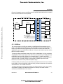
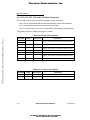
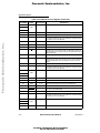
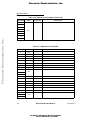
1
Freescale Semiconductor, Inc...
Freescale Semiconductor, Inc.
MPC823ADSDB
User’s Manual
Motorola reserves the right to make changes without further notice to any products herein. Motorola makes no warranty, representation or guarantee regarding
the suitability of its products for any particular purpose, nor does Motorola assume any liability arising out of the application or use of any product or circuit, and
specifically disclaims any and all liability, including without limitation consequential or incidental damages. "Typical" parameters can and do vary in different
applications. All operating parameters, including "Typicals" must be validated for each customer application by customer's technical experts. Motorola does not
convey any license under its patent rights nor the rights of others. Motorola products are not designed, intended, or authorized for use as components in
systems intended for surgical implant into the body, or other applications intended to support or sustain life, or for any other application in which the failure of the
Motorola product could create a situation where personal injury or death may occur. Should Buyer purchase or use Motorola products for any such unintended
or unauthorized application, Buyer shall indemnify and hold Motorola and its officers, employees, subsidiaries, affiliates, and distributors harmless against all
claims, costs, damages, and expenses, and reasonable attorney fees arising out of, directly or indirectly, any claim of personal injury or death associated with
such unintended or unauthorized use, even if such claim alleges that Motorola was negligent regarding the design or manufacture of the part. Motorola and
are registered trademarks of Motorola, Inc. Motorola, Inc. is an Equal Opportunity/Affirmative Action Employer.
© 1997 Motorola, Inc. All Rights Reserved.
For More Information On This Product,
Go to: www.freescale.com
Freescale Semiconductor, Inc...
Freescale Semiconductor, Inc.
PowerPC™ is a registered trademark of IBM Corporation and is used by Motorola under license from IBM.
I2C™ is a registered tradmeark of Philips Corporation.
All other trademarks are the property of their respective owners.
For More Information On This Product,
Go to: www.freescale.com
Freescale Semiconductor, Inc.
Freescale Semiconductor, Inc...
SECTION 1
INTRODUCTION
This document is the MPC823ADS daughterboard operation guide. The daughterboard
encompasses the MPC823 device along with some necessary logic that must be close to
the MPC823 and peripherals. These peripherals are dedicated to the MPC823, but are not
necessarily required for any other member of the MPC8xx Family. The daughterboard has
two sets of matching connectors—one set on the print side (on the bottom of the board) and
one on the component side (on the top of the board). Those on the print side connect to a
matching set found on the MPC8xxFADS, while those on the component side are to serve
hardware expansion via a dedicated adaptor. Also a set of logic analyzer connectors is
featured matching the new high-density HP16500 logic analyzer adaptors to provide fast
connection to a logic analyzer while saving board space and reducing EMI.
1.1 TERMINOLOGY
• ADI—Application Development Interface
• ADS—Application Development System
• BCSR—Board Control and Status Register
• BGA—Ball Grid Array
• DB—Daughterboard
• GPCM—General-Purpose Chip-Select Machine
• GPL—General-Purpose Line (associated with the UPM)
• I/R—Infra-Red
• Spec—Engineering Specification Document
• UPM—User Programmable Machine
• ZIF—Zero Input Force
1.2 RELATED DOCUMENTATION
• MPC823 User’s Manual
• ADI Board Specification
• MPC8xxFADS User’s Manual
• Analog Devices’ ADV7176 Data Sheet at http://www.analog.com/products/sheets/
ADV7176.html.
• Philip’s PDIUSBP11 Data Sheet. May be obtained from http://
www.semiconductors.philips.com/acrobat/4417.pdf
MOTOROLA
MPC823ADSDB USER’S MANUAL
For More Information On This Product,
Go to: www.freescale.com
1-1
Freescale Semiconductor, Inc.
Introduction
1.3 SPECIFICATIONS
The MPC823ADS daughterboard specifications are shown in Table 1-1
Table 1-1. MPC823ADS Daughterboard Specifications
CHARACTERISTICS
Microprocessor
Addressing
Total address range:
Freescale Semiconductor, Inc...
SPECIFICATIONS
MPC823 @ 50MHz
4G Internal
64M External*
Operating temperature
0OC – 30OC
Storage temperature
-25OC – 85OC
Relative humidity
5% – 90% (non-condensing)
Dimensions:
Length
Width
Thickness
5.87" (149mm)
4.37" (111mm)
0.063" (1.6mm)
NOTE:
* denotes the maximum contiguous block of memory that may be accessed. It can reside, however, anywhere
within the 4G addressing space.
1.4 FEATURES
• MPC823 Operation At a Maximum 50MHz
• Onboard Video Support Using the AD7176 Video Encoder with Shutdown Option
• RGB, Composite and S-Video Connection Options
• LCD Panel Connection Support with 4-Bit per Color Support
• USB Port with Shutdown Option (BCSR-Controlled). Support for Both Type A and B
USB Connectors.
• USB Port Speed Control (BCSR-driven)
• 5V Supply for USB Port (BCSR-controlled)
• Selectable KAPWR Source—3.3V or Externally Supplied
• Selectable VDDL Source—3.3V or 2.2V
• Selectable Clock Source—32768Hz Crystal Resonator or 4MHz Clock Generator That
Can be Easily Changed to Any 3.3V-Powered Oscillator with a 3–5MHz Frequency
Range
• On-Board Expansion Connectors, Including All MPC823 Pins and MPC8xxADS Control
and Status Signals.
• Onboard High-Density Logic Analyzer Connectors That Support Fast Connection to
HP16500 Logic Analyzer
• MPC821 Modem Tool Support
1-2
MPC823ADSDB USER’S MANUAL
For More Information On This Product,
Go to: www.freescale.com
MOTOROLA
Freescale Semiconductor, Inc.
LCD
CONNECTOR
Introduction
LOGIC ANALYZER
CONNECTOR
S-VIDEO
G
MPC823
AD7176
VIDEO
ENCODER
R
B
USB TYPE A
C
CLOCKS
USB TYPE B
Freescale Semiconductor, Inc...
MOTHERBOARD AND
EXPANSION CONNECTORS
Figure 1-1. MPC823ADS Daughterboard Block Diagram
1.5 CHANGES FROM PREVIOUS REVISION (DRAFT 0.1)
• Video controller is reset only by software via BCSR. Not affected by hard reset.
• Changed SCC2 port to MPC823ADS connection scheme. See Section 4.7
Communication Ports for more information.
• Added USB power control (BCSR-controlled) with power-on indication LED.
• Added 3.3V pull-up resistors over USB’s D+ and D- lines. Connection scheme of these
resistors depends on USB port’s speed. See Section 4.7.1 USB Port for more
information.
• Added support for MPC821 modem tool. See Section 4.8.1 MPC821 Modem Tool
Support for more information.
• The selection of power-on reset source is moved onboard from the MPC8xxFADS.
• Part numbers are provided for all connectors.
MOTOROLA
MPC823ADSDB USER’S MANUAL
For More Information On This Product,
Go to: www.freescale.com
1-3
Freescale Semiconductor, Inc.
Freescale Semiconductor, Inc...
SECTION 2
CONFIGURATION AND INSTALLATION
This section contains information about preparing, configuring, and installing the
MPC823ADS daughterboard. When you receive your daughterboard, you should unpack
the shipping carton and verify the contents against the packing list. If the contents were
damaged during shipping, call your local Motorola sales office, explain the problem, and you
should receive another package. If the contents are undamaged, save the packing slip and
start configuring the board for your design.
Caution: Avoid touching the integrated circuitry of the board with your hands since static
discharge can damage circuits.
2.1 CONFIGURING THE BOARD
Before you configure the MPC823ADS daughterboard, you may have to change the
jumpers settings before you can install the board into your system. Since they are factory
set and tested, they may not be set correctly for your particular configuration. Figure 2-1
illustrates the location of these jumpers, LEDs, and connectors on the board. The
MPC823ADS daughterboard settings contain the following parameters that you can change
for your specific configuration:
• Clock generator
• Power-on reset source
• MPC823 keep-alive power source
• MPC823 internal logic supply source
• ADV7176 video controller’s I2C free address bit
MOTOROLA
MPC823ADSDB USER’S MANUAL
For More Information On This Product,
Go to: www.freescale.com
2-1
Freescale Semiconductor, Inc.
Freescale Semiconductor, Inc...
Configuration and Installation
Figure 2-1. MPC823ADS Daughterboard Top-Side Parts Locator
2.1.1 Replacing the Clock Generator
When replacing the clock generator (U1), all you need to know is that there are two supply
levels. A 5V supply is available at Pin 14 and a 3.3V supply is available at Pin 11.
2-2
MPC823ADSDB USER’S MANUAL
For More Information On This Product,
Go to: www.freescale.com
MOTOROLA
Freescale Semiconductor, Inc.
Configuration and Installation
Figure 2-2 illustrates that a 5V oscillator (with 3.3V output only) can be used with a 14-pin
form-factor, while 3.3V oscillators can be used with an 8-pin form-factor.
14
Freescale Semiconductor, Inc...
1
5V
3.3V
GND
7
8
U1
Figure 2-2. Clock Generator (U1) Power Sources
Inserting a 14-pin form-factor 3.3V clock generator into U1 could cause permanent damage
to your device. Since the MPC823 clock input is not 5V-tolerant, any clock generator
inserted into U17 must have a 3.3V-compatible output. If you insert a 5V output clock
generator into U17, you could cause permanent damage to the MPC823 microprocessor.
MOTOROLA
MPC823ADSDB USER’S MANUAL
For More Information On This Product,
Go to: www.freescale.com
2-3
Freescale Semiconductor, Inc.
Configuration and Installation
2.1.2 Selecting the Power-On Reset Source
Freescale Semiconductor, Inc...
The functionality of the power-on reset logic changes with each revision of the MPC823. For
your purposes, this means that you may need to select a different source to generate a
power-on reset. To select your power-on reset source, you need to set J1 on the
MPC823ADS daughterboard. When the J1 jumper is between positions 1 and 2, a power-on
reset is generated by the keep-alive power rail (KAPWR). For example, when KAPWR goes
below 2.005V, a power-on reset is generated. When the J1 jumper is between positions
2 and 3, a power-on reset is generated from the main 3.3V power rail. In other words, when
the 3.3V power rail gets below 2.805V, a power-on reset is generated.
J1
J1
1
1
KEEP-ALIVE POWER RAIL
MAIN POWER RAIL
Figure 2-3. Power-On Reset Source
2.1.3 Selecting the VDDL Source
The J3 jumper is used to select the VDDL, which supplies the MPC823’s internal logic.
When the J3 jumper is between positions 1and 2, VDDL is supplied with 3.3V of power.
When the J3 jumper is between positions 2 and 3, VDDL is supplied with 2.2V of power. The
J3 jumper is factory set between positions 1 and 2.
J3
1
J3
1
3.3V VDDL
2V VDDL
Figure 2-4. VDDL Source
2-4
MPC823ADSDB USER’S MANUAL
For More Information On This Product,
Go to: www.freescale.com
MOTOROLA
Freescale Semiconductor, Inc.
Configuration and Installation
2.1.4 Selecting the Keep-Alive Power Source
The J2 jumper is used to select the keep-alive power source. When the J2 jumper is
between positions 1 and 2, the keep-alive power is fed from the main 3.3V bus. When you
need to connect an external power source (such as a battery) to the keep-alive power rail,
it should be connected between positions 2 (the positive pole) and 3 (GND) without any
jumper connected.
J2
J2
1
Freescale Semiconductor, Inc...
3.3V
3.3V
1
KAPWR
KAPWR
+
GND
GND
–
KAPWR FROM 3.3V
KAPWR FROM EXTERNAL
POWER SUPPLY
EXTERNAL
POWER SUPPLY
Figure 2-5. Keep-Alive Power Source
2.1.5 Selecting the ADV7176’s I2C Slave Address
The ADV7176 video encoder has two possible slave addresses that can be selected using
the J5 jumper. When J5 is between positions 1 and 2, the slave address is 1101011. When
the jumper is between positions 2 and 3, the slave address is 1101010. The J5 jumper is
factory set to positions 2 and 3.
J5
J5
1
1
SLAVE ADDRESS 1101011
SLAVE ADDRESS 1101010
2C
Figure 2-6. ADV7176 I
Slave Address
2.2 INSTALLING THE DAUGHTERBOARD
To begin with, the MPC823ADS daughterboard must be plugged into the MPC8xxFADS
motherboard. Make sure there is no power connected to either board. Place the
MPC823ADS daughterboard over the motherboard connectors so that the PM1–PM4 of
both boards are aligned. Then press the board gently into position. This process should be
relatively unproblematic since the connectors are arranged in a nonsymmetrical form.
MOTOROLA
MPC823ADSDB USER’S MANUAL
For More Information On This Product,
Go to: www.freescale.com
2-5
Freescale Semiconductor, Inc.
SECTION 3
OPERATION
Freescale Semiconductor, Inc...
This section contains the necessary information you need to operate the MPC823ADS
daughterboard.
3.1 INDICATORS
The MPC823ADS daughterboard does not have any switches, but it has eight indicators:
• Four GND bridges
• A 3.3V indicator
• A USB-On indicator
• A USB power indicator
• A VDO-On indicator
3.1.1 GND Bridges
There are four GND bridges on the MPC823ADS daughterboard. They can be used to assist
you with easy ground access points for general measurements and a logic analyzer
connection.
Warning: The onboard GND bridges physically resemble the J4 jumper and you should
take care not to mistake it for a GND jumper. Doing so could cause permanent
damage to your MPC823ADS daughterboard or MPC8xxFADS motherboard.
When you are connecting to a GND bridge, use only insulated GND clips to
keep from damaging the board.
3.1.2 3.3V Indicator
The yellow 3.3V LED (LD1) indicates that the 3.3V power bus is receiving power from the
MPC823ADS board.
3.1.3 USB-On Indicator
The yellow USB-On indicator LED (LD2) indicates that the USB transceiver is enabled for
USB reception (the receive buffer is driven towards the MPC823). When it is not lit, the
receive buffer is three-stated and the USB pins can be used for another function. See
BCSR4 of the MPC8xxFADS User’s Manual for more information.
MOTOROLA
MPC823ADSDB USER’S MANUAL
For More Information On This Product,
Go to: www.freescale.com
3-1
Freescale Semiconductor, Inc.
Operation
3.1.4 USB-PWR Indicator
The yellow USB-PWR LED indicates that the 5V power is being driven to pin 1 of the USB
connectors P3 and P4. When the it is not lit, it indicates that Pin 1 of these connectors is
floating and the MPC823ADS daughterboard can be connected to an external USB master.
See BCSR4 of the MPC8xxFADS User’s Manual for more information.
Freescale Semiconductor, Inc...
3.1.5 VDO On Indicator
When the yellow VDO On LED is lit, it may indicate that the video encoder is enabled on the
I2C® bus. This is a soft indication since the ADV7176 is enabled and disabled via the I2C
port. This indication allows your application software to visually indicate that the video
encoder is on. See BCSR4 of the MPC8xxFADS User’s Manual for more information.
3.1.6 Memory Map
The memory map is the same on all daughterboards. See Section 3.3 Memory Map of the
MPC8xxFADS User’s Manual for more information.
3.1.7 Programming the MPC8xx Registers
To program the MPC8xx registers, see Section 3.1.7 Programming the MPC8xx
Registers of the MPC8xxFADS User’s Manual.
3-2
MPC823ADSDB USER’S MANUAL
For More Information On This Product,
Go to: www.freescale.com
MOTOROLA
Freescale Semiconductor, Inc.
SECTION 4
FUNCTIONALITY
Freescale Semiconductor, Inc...
This section describes these main functions of the MPC823ADS daughterboard:
• Reset
• Interrupts
• Clock generator
• Video support
• LCD panel support
• PCMCIA port
• Communication ports and their expansion
• Board control and status register
• Debug port
4.1 RESET
There are three sources of reset for the MPC823 device:
• Power-on reset
• Hard reset
• Soft reset
4.1.1 Power-On Reset
On the MPC823ADS daughterboard, a power-on reset can be generated from a keep-alive
power bus or a main power bus. A jumper is used to select one of these sources. When you
select the keep-alive power bus, a dedicated voltage detector made by Seiko
(S-8051HN-CD-X), which has a detection voltage range of 1.795–2.005V, generates the
power-on reset. During a keep-alive power-on, or when there is a voltage drop of that input
into the above range, a power-on reset is generated (the PORESET input of the MPC823 is
asserted for approximately 4 seconds).
When you select the main power bus, a dedicated voltage detector made by Seiko
(S-8052ANY-NH-X), with a detection voltage range of 2.595–2.805V, generates the
power-on reset. During a main 3.3V bus power-on, or when there is a voltage drop of that
input into the above range, a power-on reset is generated (the PORESET input of the
MPC823 is asserted for approximately 4 seconds). The main power-on reset also generates
a power-on reset to all logic on the motherboard.
MOTOROLA
MPC823ADSDB USER’S MANUAL
For More Information On This Product,
Go to: www.freescale.com
4-1
Freescale Semiconductor, Inc.
Functionality
The power-on reset configuration is read by the MPC823 when PORESET is asserted to the
MPC82. See Section 4.1.6.1 Power-On Reset Configuration of the MPC8xxFADS User’s
Manual for more information.
4.1.2 Hard Reset
A hard reset is generated from four possible sources:
• A main power-on reset
• A manual hard reset generated on the motherboard
Freescale Semiconductor, Inc...
• A debug port hard reset
• An internal source of the MPC823
When the open-drain HRESET signal is asserted, hard reset configuration data is driven on
the data bus by the motherboard logic. See Section 4.1.6.2 Hard Reset Configuration of
the MPC8xxFADS User’s Manual for details.
4.1.3 Soft Reset
A soft reset is generated from three possible sources:
• The debug port controller on the motherboard
• A manual soft reset generated on the motherboard
• An internal source of the MPC823
The motherboard logic makes a soft reset configuration available to the MPC823 when a
soft reset is generated to the MPC823. See Section 4.1.6.2 Soft Reset Configuration of
the MPC8xxFADS User’s Manual for details.
4.2 INTERRUPTS
The only external interrupt that is applied to the MPC823 via its interrupt controller is the
abort (NMI) interrupt, which is generated by a push-button and logic residing on the
motherboard.
4.3 CLOCK GENERATOR
Although most of the clock generator logic is found on the daughterboard, it is explained in
detail in the motherboard manual since it is common to all daughterboards. See Section 4.3
Clock Generator of the MPC8xxFADS User’s Manual for more information.
4-2
MPC823ADSDB USER’S MANUAL
For More Information On This Product,
Go to: www.freescale.com
MOTOROLA
Freescale Semiconductor, Inc.
Functionality
4.4 VIDEO SUPPORT
Freescale Semiconductor, Inc...
The MPC823ADS daughterboard has full onboard support for video. A direct connection can
be made between the MPC823ADS daughterboard and a video monitor supporting either
RGB, Composite or S-Video input standards.
The Analog Devices ADV7176, which is an NTSC/PAL video encoder, can be controlled by
the MPC823 I2C port. Since an I2C slave has a unique address, you can connect another
I2C slave with the expansion connector without any buffering. The ADV7176 can be put in
low-power mode while another I2C device is used offboard via the expansion connectors.
The ADV7176 is clocked by an onboard 27MHz clock generator (U11), which can be
three-stated with the VDOEXTCK signal from the motherboard’s board control and status
register 4 (BCSR4). When the clock generator is disabled (three-stated), the MPC823 can
clock the ADV7176 if 27MHz can be achieved using a multiplication factor (MF).
Warning:
If U1 is enabled and the MPC823 drives the PD3/VDOCLK signal to the ADV7176, it could
cause permanent damage to the MPC823 and 27MHz clock generator.
Using BCSR4’s VDORST signal, the software can reset the video encoder. Notice that this
is a falling-edge reset, instead of a level-sensitive reset. The video encoder supports three
types of video inter-connects:
• S-Video via the P10 connector on the daughterboard
• Composite video via the P11 connector on the daughterboard
• RGB video via the P12–P14 connectors on the daughterboard
You can enable or disable the video encoder at any time via its I2C port. For more
information see the ADV7176 data sheet for more information.
4.4.1 ADV7176 Power Considerations
The ADV7176 is an analog device, which requires a quiet power supply. Therefore, its
power supply is filtered by a ∏ network and is isolated from the noisy digital supply. The
ground of the device is isolated from the digital ground by means of a peninsula to avoid
noisy digital GND currents. The D/As of the ADV7176 require a stable and clean 1.2V
voltage reference, which can be obtained from U3 (an AD589 voltage reference device).
4.5 LCD PANEL SUPPORT
A dedicated LCD connector is provided with your board to allow connection to an LCD panel.
This connector contains the MPC823 Port D pins and any additional LCD Port B pins. When
the video encoder is in low-power mode, you can connect to an LCD panel with the port D
pin and three Port B pins (the Port B pins add 1 bit per color which makes it a 4,4,4 color
word). The LCD connector is a superset of the LCD connector that exists on the
MPC821ADS, which makes it easy to move tools between the two boards and to connect
the additional color bits.
MOTOROLA
MPC823ADSDB USER’S MANUAL
For More Information On This Product,
Go to: www.freescale.com
4-3
Freescale Semiconductor, Inc.
Functionality
To make connecting even easier, there are 5V supply pins available on the additional pins
of the LCD connector. For a signal description of the LCD connector, see Table 5-8 in this
manual.
4.6 PCMCIA PORT
Freescale Semiconductor, Inc...
The MPC823 has only one PCMCIA port and it resides on the PCMCIA port B pins. It is
routed to the PCMCIA port on the MPC823AADS. The default hard reset configuration of
the MPC823ADS sets up these pins as PCMCIA port B pins.
The PCMCIA port on the MPC823ADS is intended to reside on the PCMCIA port A of the
MPC823. Therefore, there is a cross between PCMCIA ports A and B on the motherboard
connectors. The port B signals are connected in the same place that is reserved for the
PCMCIA port A pins. For more information, see Section 4.10 PCMCIA Port of the
MPC8xxFADS User’s Manual.
4.7 COMMUNICATION PORTS
The MPC823 has the following communication ports that can be used in a variety of ways
on the MPC823ADS daughterboard:
• A USB port that is connected to a USB transceiver onboard
• A serial communication controller (SCC2) that can operate as an Ethernet port, an
infra-red port (IrDA), or an RS-232 port #2.
• A serial management controller (SMC1) that is connected to RS-232 port #1 of the
MPC823ADS
• A serial management controller (SMC2) that is not used onboard.
• An inter-integrated circuit (I2C) that is used to program the video encoder
• A serial peripheral interface (SPI) that is not used onboard
Using BCSR1 or BCSR4, the software can enable or disable all of the communication ports.
See BCSR1 and BCSR4 in the MPC8xxFADS User’s Manual for details.
To protect against possible contention, the RxD lines of the Ethernet port, IrDA port, and
RS-232 port #2 of the MPC823ADS are multiplexed to the RXD2 input. Use the appropriate
enable bits in the BCSR1 to select between the three RxD lines. When one and only one of
the ETH_EN, IRD_EN, or RS_EN2 bits in the BCSR1 is enabled, its respective
communication port RxD line is driven to RXD2 of the MPC823. If two or more of these lines
are simultaneously enabled and then 0 is driven to RXD2. When none of them are asserted,
the output of the mux is three-stated and the RXD2 line of the MPC823 can be used for
another function.
4-4
MPC823ADSDB USER’S MANUAL
For More Information On This Product,
Go to: www.freescale.com
MOTOROLA
Freescale Semiconductor, Inc.
Functionality
Figure 4-1 illustrates how to connect Ethernet, IrDA, and RS-232 Serial Port #2 is connected
to the SCC2 and selection is accomplished.
MPC823ADS DAUGHTERBOARD
MPC8XXFADS
PM3
PD3
ETHERNET
TXD
MPC823
74LCX257
RXD
3
Freescale Semiconductor, Inc...
TXD2
RXD2
MUX 8:1
IRDA
TXD
Z
5
6
0,1,2,4,7
OE 2 1 0
RXD
RS-232 #2
TXD
RXD
BCSR1
RS_EN2
IRD_EN
ETH_EN
Figure 4-1. SCC2 Connection Scheme
4.7.1 USB Port
The universal serial bus (USB) port resides on the MPC823ADS daughterboard and is
driven by the USB port of the MPC823. A dedicated USB transceiver (the PDIUSBP11 by
Philips) is provided with the daughterboard. Also provided is a three-state buffer that
separates this port from the MPC823’s USB port, so that you can disable a port and use the
MPC823 USB pins offboard.
To properly support the different speeds of the USB, the detachable 3.3V pull-up resistors
are provided on the D+ and D- lines of the USB. They are controlled by the USB_SPD bit of
the BCSR4. When the USB_SPD bit is in low-speed mode, D- is pulled up while D+
continues to float. When the USB_SPD bit is in high-speed mode, D+ is pulled up while Dcontinues to float. The USB_SPD bit is connected to the SPEED input of the USB
transceiver, which sets it to the preferred operation range.
In Revision ENG, a 5V power source is provided to the USB connector and it is controlled
by the USB_VCC0 bit in the BCSR4. When the USB_VCC0 bit is driven low, a 5V source is
connected to Pin 1 of the USB connectors.
To support both types of physical connections, two USB connectors (Type A and Type B)
are provided in parallel. For additional information on USB pin connection to those
connectors, see BCSR4 later in this manual.
MOTOROLA
MPC823ADSDB USER’S MANUAL
For More Information On This Product,
Go to: www.freescale.com
4-5
Freescale Semiconductor, Inc.
Functionality
4.7.2 Ethernet Port
The SCC2 of the MPC823 can operate as an Ethernet port. It can be connected to the
ethernet transceiver on the MPC823ADS if the ETH_EN bit of the BCSR1 is asserted and
the IRD_EN and RS_EN2 bits in the same register are inactive. For more information, see
Section 4.11.3 Board Control and Status Register 1 of the MPC8xxFADS User’s Manual.
Freescale Semiconductor, Inc...
4.7.3 Infra-Red Port
The SCC2 of the MPC823 can operate as a fast IrDA port. It can be connected to the fast
IrDA transceiver on the MPC823ADS if the IRD_EN bit of the BCSR1 is asserted and the
ETH_EN and RS_EN2 bits in the same register are inactive. For more information, see
Section 4.11.3 Board Control and Status Register 1 and Section 4.9.2 Infra-Red Port
of the MPC8xxFADS User’s Manual.
4.7.4 RS-232 Ports
There can be two RS-232 ports with this application. The RS-232 port #1 of the
MPC823ADS is connected to the SMC1 of the MPC823. The RS-232 port #2 of the
MPC823ADS can be connected to the SCC2 of the MPC823 if the RS_EN2 bit in the BCSR1
is asserted and the ETH_EN and IRD_EN bits in the same register are inactive.
Both ports can be enabled or disabled at any time using the BCSR1. For more information,
see Section 4.11.3 Board Control and Status Register 1 and Section 4.9.3 RS-232 Port
of the MPC8xxFADS User’s Manual.
4.8 COMMUNICATION PORT EXPANSION
On the MPC823ADS board, all of the MPC821 and MPC860 communication port pins were
available at a 96-pin DIN 41612 connector (P13). This connector is compatible with P8 of
the MPC8xxFADS. Since the MPC823 has a unique and partial set of communication ports,
the pin assignment is different. Therefore, it is important that you carefully examine any tool
you create for this connector before it is connected to an MPC8xxFADS with a
daughterboard attached to it.
4.8.1 MPC821 Modem Tool Support
The MPC821 modem tool uses the MPC821 time-slot assigner (TSA) TDM ports A and B.
However, the MPC823 has only one TDM port. Therefore, the data portion of the tool, which
originally used TDM port B, is now multiplexed with the voice portion so that they both reside
on TDM port A of the MPC823. To support this multiplexing, two signals are introduced from
the MPC823ADS; MODEM_EN, which enables the mux, and MDM_AUD, which selects
between the data and voice codecs of the modem tool.
4-6
MPC823ADSDB USER’S MANUAL
For More Information On This Product,
Go to: www.freescale.com
MOTOROLA
Freescale Semiconductor, Inc.
Functionality
Figure 4-2 illustrates the modem tool support logic.
MPC823ADS DAUGHTERBOARD
PX3
MPC823
PC7
PC7/USBTXP
PB22
PB31
PB22
PB31
PB28
PA11
PB28
Freescale Semiconductor, Inc...
PM3
PB18
PB19
PA9
PA9/L1TXDA
1
PA8/L1RXDA
OE 0
S
1
PA7/L1RCLKA
MPC8XXFADS
PD3
OE 0
S
PA10
PA8
PA2
PA7/ETHTCK
PA5
PA5/ETHTCK
P8
MPC821 MODEM TOOL
B14
HOOK CONTROL
B28
RING DETECT
B10
MUTE
B1
RESET~ (DATA)
B4
RESET~ (VOICE)
A18
A20
DIN (DATA)
DIN (VOICE)
A19
DOUT (DATA)
A21
DOUT (VOICE)
A14
SCLK (DATA)
A9
SCLK (VOICE)
A11
PC6/USBTXN
1
PC4/L1RSYNCA
PB26 /I2CCLK
PB27/I2CDAT
PB29
PB30
OE 0
S
PC6
PC4
PB26
PB27
PB29
PB30
PB15
PA6/ETHRCK
ETHRCK
B29
FSYNC (DATA)
B31
FSYNC (VOICE)
B6
HC1 (VOICE)
HC0 (VOICE)
HC1 (DATA)
B5
B3
B2
HC0 (DATA)
B17
PB15 (CLK SOURCE)
A10
PA6 (CLK SOURCE)
MDM_AUD~
MODEMEN~
Figure 4-2. Modem Tool Support Logic
MOTOROLA
MPC823ADSDB USER’S MANUAL
For More Information On This Product,
Go to: www.freescale.com
4-7
Freescale Semiconductor, Inc.
Functionality
Before operating the modem tool, the following conditions should be met.
• The Ethernet, USB, and video ports must be disabled since they only use a few lines
that are common to the modem application. These ports must be disabled when their
respective enable bits in the BCSR1 and BCSR4 are negated. This does not apply for
the video encoder, however, which is enabled and disabled with the I2C port. The video
encoder uses the I2C port for initializations, but once they are complete the port can be
used for other applications.
• Use PB19 for hook control, instead of PB18, which was used with the MPC821.
Freescale Semiconductor, Inc...
• Assert the MODEM_EN bit in the BCSR4. For more information, see BCSR4 in the
MPC8xxFADS User’s Manual.
• With the MPC821, one of the optional clock sources for the modem was PB15, which
does not exist on the MPC823. Since it was not used with the working application, no
replacement was provided for this signal and it remains unconnected.
• To select between the voice and data portions of the modem, set the MDM_AUD bit in
the BCSR4. For more information, see BCSR4 in the MPC8xxFADS User’s Manual).
4.9 BOARD CONTROL AND STATUS REGISTER
Most board control and status register (BCSR) control signals and some status signals are
available on the motherboard connectors and the expansion connectors. The BCSR
controls most of the functions available on the MPC823ADS daughterboard and on the
MPC8xxFADS. See Section 4.11 Board Control and Status Register of the
MPC8xxFADS User’s Manual for more information.
4.10 DEBUG PORT
The MPC823 uses the motherboard connectors to connect to the MPC823ADS board’s
debug port controller. For details, see Section 4.12 Debug Port Controller in the
MPC8xxFADS User’s Manual.
The debug port on the daughterboard resides on the MPC823 JTAG port. There is no
support for the debug port to reside on the PCMCIA port B pins. Since the VFLS[0:1] pins,
which are usually required by the debug port controller to monitor the run/debug mode
status, are being used for PCMCIA port B, you must use the FRZ signal that is connected
to the MPC823ADS debug port controller.
4-8
MPC823ADSDB USER’S MANUAL
For More Information On This Product,
Go to: www.freescale.com
MOTOROLA
Freescale Semiconductor, Inc.
SECTION 5
SIGNAL DESCRIPTIONS
Freescale Semiconductor, Inc...
This section contains signal information for supporting, maintaining, and connecting to the
MPC823ADS daughterboard.
5.1 INTERCONNECT SIGNALS
The MPC823ADS daughterboard uses the following connectors to interconnect with
external devices.
• P1, P2, P5, P6, P8, and P9—Logic analyzer connectors
• P3 and P4—USB connectors
• P7—LCD panel connector
• P10, P11, P12, P13, and P14—Video connectors
• PM1, PM2, PM3, and PM4—Motherboard connectors
• PX1, PX2, PX3, and PX4—Expansion connectors
• MPC823ADS P8—Serial port expansion connector1
5.1.1 P1, P2, P5, P6, P8, and P9–Logic Analyzer Connectors
These connectors are 38-pin, receptacle MICTOR connectors manufactured by AMP. Each
connector connects to a dedicated adaptor for an HP16500 Series logic analyzer, which
interconnects to two 16-bit pods. Since all the signals on these connectors are also on the
motherboard connectors and expansion connectors, they are described in the MPC823
User’s Manual as well.
1. This
connector is located on the motherboard. It is documented here since its contents depends on the
daughterboard.
MOTOROLA
MPC823ADSDB USER’S MANUAL
For More Information On This Product,
Go to: www.freescale.com
5-1
Freescale Semiconductor, Inc.
Signal Descriptions
Freescale Semiconductor, Inc...
Table 5-1. P1 Interconnect Signals
PIN NUMBER
SIGNAL
PIN NUMBER
SIGNAL
1
—
2
—
3
GND
4
—
5
TEA
6
7
SDRMCS
8
BSWE0
9
CS5
10
BSWE1
11
CE1B
12
BSWE2
13
CE2B
14
BSWE3
15
BR
16
DRM_W
17
BG
18
EDOOE
19
BB
20
GPL2
21
BI
22
GPL3
23
BURST
24
GPL4A
25
—
26
GPL4B
27
—
28
GPL5A
29
BVS2
30
GPL5B
31
BVS1
32
F_CS
33
BWP
34
BCSRCS
35
BCD2
36
DRMCS1
37
BCD1
38
DRMCS2
NOTE: — is not connected.
5-2
MPC823ADSDB USER’S MANUAL
For More Information On This Product,
Go to: www.freescale.com
MOTOROLA
Freescale Semiconductor, Inc.
Signal Descriptions
Table 5-2. P2 Interconnect Signals
PIN NUMBER
SIGNAL
PIN NUMBER
SIGNAL
1
—.
2
—
3
GND
4
—
6
TS
8
A16
TS
10
A17
11
TA
12
A18
13
R_W
14
A19
15
REG_A
16
A20
17
TSIZ1
18
A21
19
A6
20
A22
21
A7
22
A23
23
A8
24
A24
25
A9
26
A25
27
A10
28
A26
29
A11
30
A27
31
A12
32
A28
33
A13
34
A29
35
A14
36
A30
37
A15
38
A31
5
TA
7
Freescale Semiconductor, Inc...
9
NOTE: — is not connected.
MOTOROLA
MPC823ADSDB USER’S MANUAL
For More Information On This Product,
Go to: www.freescale.com
5-3
Freescale Semiconductor, Inc.
Signal Descriptions
Table 5-3. P5 Interconnect Signals
Freescale Semiconductor, Inc...
PIN NUMBER
SIGNAL
PIN NUMBER
SIGNAL
1
—
2
—
3
GND
4
—
5
—
6
—
7
DSCK
8
DSDI
9
BBVD2
10
—
11
BBVD1
12
DSDO
13
BRDY
14
FRZ
15
ALE_B
16
NMI
17
SPKROUT
18
IRQ1
19
MODCK1
20
IRQ2
21
MODCK2
22
IRQ7
23
WAIT_B
24
—
25
RSTCNF
26
EXTCLK
27
TEXP
28
—
29
HRESET
30
DP0
31
SRESET
32
DP1
33
PORST
34
DP2
35
—
36
DP3
37
—
38
V3.3
NOTE: — is not connected.
5-4
MPC823ADSDB USER’S MANUAL
For More Information On This Product,
Go to: www.freescale.com
MOTOROLA
Freescale Semiconductor, Inc.
Freescale Semiconductor, Inc...
Table 5-4. P6 Interconnect Signals
PIN NUMBER
SIGNAL
PIN NUMBER
SIGNAL
1
—
2
—
3
GND
4
—
5
—
6
SYSCLK
7
USBRXD
8
9
USBOE
10
—
11
USBRXP
12
—
13
USBRXN
14
—
15
USBTXP
16
PC12
17
USBTXN
18
TPSQEL
19
TXD2
20
PC14
21
RXD2
22
BINPAK
23
TMS
24
—
25
I2CDAT
26
SPARE2
27
I2CCLK
28
—
29
PB28
30
RSDTR1
31
PB29
32
—
33
PB30
34
RSDTR2
35
LCD_A
36
RSRXD1
37
TRST
38
RSTXD1
NOTE: — is not connected.
MOTOROLA
MPC823ADSDB USER’S MANUAL
For More Information On This Product,
Go to: www.freescale.com
5-5
Freescale Semiconductor, Inc.
Signal Descriptions
Freescale Semiconductor, Inc...
Table 5-5. P8 Interconnect Signals
PIN NUMBER
SIGNAL
PIN NUMBER
SIGNAL
1
—
2
3
GND
4
5
—
6
7
—
8
9
—
10
11
PA4
12
—
13
ETHTCK
14
HSYNC
15
ETHRCK
16
VSYNC
17
PA7
18
BLANK
19
PA8
20
FIELD
21
PA9
22
VD0
23
ETHLOOP
24
VD1
—
—
VDOCLK
—
25
TPFLDL
26
VD2
27
E_RENA
28
VD3
29
E_CLSN
30
VD4
31
PB16
32
VD5
33
LCD_C
34
VD6
35
E_TENA
36
VD7
37
LCD_B
38
SPARE3
NOTE: — is not connected.
5-6
MPC823ADSDB USER’S MANUAL
For More Information On This Product,
Go to: www.freescale.com
MOTOROLA
Freescale Semiconductor, Inc.
Signal Descriptions
Freescale Semiconductor, Inc...
Table 5-6. P9 Interconnect Signals
PIN
NUMBER
SIGNAL
PIN NUMBER
SIGNAL
1
—
2
—
3
GND
4
—
5
—
6
—
7
D0
8
D16
9
D1
10
D17
11
D2
12
D18
13
D3
14
D19
15
D4
16
D20
17
D5
18
D21
19
D6
20
D22
21
D7
22
D23
23
D8
24
D24
25
D9
26
D25
27
D10
28
D26
29
D11
30
D27
31
D12
32
D28
33
D13
34
D29
35
D14
36
D30
37
D15
38
D31
NOTE: — is not connected.
MOTOROLA
MPC823ADSDB USER’S MANUAL
For More Information On This Product,
Go to: www.freescale.com
5-7
Freescale Semiconductor, Inc.
Signal Descriptions
5.1.2 P3 and P4–USB Connectors
The MPC823ADS daughterboard supports both Type A and Type B USB connectors. P3 is
Type B and P4 is Type A (both of which are manufactured by AMP). Their pinout is identical
and their signals are shown in Table 5-7.
Freescale Semiconductor, Inc...
Table 5-7. P3 and P4 Interconnect Signal
PIN NUMBER
SIGNAL
INPUT/OUTPUT
1
USBPWR
O
DESCRIPTION
USB Power. To support USB Host function, this pin can be driven
with a 5V BCSR–controlled source. See BCSR4 in the
MPC8xxFADS User’s Manual for more information. When the
MPC823 daughterboard is configured as a USB slave, the power
should be turned off for that pin.
2
D–
I/O
USB negative (differential) data line.
3
D+
I/O
USB positive (differential) data line.
4
GND
—
MPC823 daughterboard Ground plane.
5.1.3 P7–LCD Panel Connector
The LCD panel connector is a 40-pin (2x20) header connector, which is compatible with the
LCD panel connector that is on the MPC821ADS, plus an expansion to support the 4-bit per
color added for the MPC823. To allow for an easier migration for MPC821 users, the signals
are assigned so that panels that were connected to the MPC821ADS can be connected
directly. The P7 are shown in Table 5-8.
Table 5-8. P7 Interconnect Signals
PIN
NUMBER
SIGNAL
INPUT/OUTPUT
DESCRIPTION
1
SHIFT_C
I/O
LCD Shift Clock
GND
—
—
5
LOE
I/O
Output Enable for TFT Displays or Passive Panels LCD_AC Signal
6
GND
—
—
7
HSYNC
I/O
Display Line Beginning Mark
2
3
4
8
GND
—
—
9
VSYNC
I/O
New Frame Beginning Mark
GND
—
—
13
LD0
I/O
LCD Data Line 0
14
GND
—
—
10
11
12
5-8
MPC823ADSDB USER’S MANUAL
For More Information On This Product,
Go to: www.freescale.com
MOTOROLA
Freescale Semiconductor, Inc.
Signal Descriptions
Table 5-8. P7 Interconnect Signals (Continued)
Freescale Semiconductor, Inc...
PIN
NUMBER
SIGNAL
INPUT/OUTPUT
DESCRIPTION
15
LD1
I/O
LCD Data Line 1
16
GND
—
—
17
LD2
I/O
LCD Data Line 2
18
GND
—
—
19
LD3
I/O
LCD Data Line 3
20
GND
—
—
21
LD4
I/O
LCD Data Line 4
22
GND
—
—
23
LD5
I/O
LCD Data Line 5
24
GND
—
—
25
LD6
I/O
LCD Data Line 6
26
GND
—
—
27
LD7
I/O
LCD Data Line 7
28
GND
—
—
29
LD8
I/O
LCD Data Line 8
30
GND
—
—
—
—
35
LCD_A
I/O
Mux’ed on PB31. The MSB for the LCD Data Word.
36
VCC
O
5V Supply
37
LCD_B
I/O
Mux’ed on PB19. The Middle of the Additional Three LCD Data Bits.
31
32
Pin is Cut to Allow 30-Pin Connector Insertion
33
34
38
VCC
O
5V Supply
39
LCD_C
I/O
Mux’ed on PB17. The LSB of the Additional Three LCD Data Bits.
40
VCC
O
5V Supply
MOTOROLA
MPC823ADSDB USER’S MANUAL
For More Information On This Product,
Go to: www.freescale.com
5-9
Freescale Semiconductor, Inc.
Signal Descriptions
5.1.4 P10, P11, P12, P13, and P14–Video Connectors
The following connectors support various standards in video connectivity:
• P10 is a 4-pin subminiature DIN connector that conforms to the S-Video standard
• P11 is a coaxial RCA connector that carries composite video
• P12, P13, and P14 carry red, green, and blue (RGB) video signals (correspondingly)
The signals are shown in Tables 5-9 through 5-13 below.
Freescale Semiconductor, Inc...
Table 5-9. P10 Interconnect Signals
PIN NUMBER
SIGNAL
INPUT/OUTPUT
DESCRIPTION
1
—
—
Unused. Nonexistent with This Connector, Although Counted for Pin
Numbering. This Connector is a Subset of the DIN-8 Connector.
3
GND
—
—
4
—
—
Unused. Nonexistent with This Connector, Although Counted for Pin
Numbering. This Connector is a Subset of the DIN-8 Connector.
5
GND
—
—
6
Green/Luma/Y
O
Luma signal. From the ADV7176 Video Encoder.
7
—
—
Unused. Nonexistent with This Connector, Although Counted for Pin
Numbering. This Connector is a Subset of the DIN-8 Connector.
8
Red/Chroma/V
O
Chroma signal.
2
NOTE: — is not connected.
Table 5-10. P11 Interconnect Signals
PIN NUMBER
SIGNAL
INPUT/OUTPUT
1
GND
—
—
2
Composite
O
Composite Video from the ADV7176 Video Encoder
5-10
DESCRIPTION
MPC823ADSDB USER’S MANUAL
For More Information On This Product,
Go to: www.freescale.com
MOTOROLA
Freescale Semiconductor, Inc.
Signal Descriptions
Freescale Semiconductor, Inc...
Table 5-11. P12 Interconnect Signals
PIN NUMBER
SIGNAL
INPUT/OUTPUT
DESCRIPTION
1
GND
—
—
2
Red/Chroma/V
O
Red Component of RGB. Generated by the ADV7176 Video
Encoder
Table 5-12. P13 Interconnect Signals
PIN
NUMBER
SIGNAL
INPUT/OUTPUT
DESCRIPTION
1
GND
—
—
2
Green/Luma/Y
O
Green Component of RGB. Generated by the ADV7176 Video
Encoder.
Table 5-13. P14 Interconnect Signals
PIN
NUMBER
SIGNAL
INPUT/OUTPUT
1
GND
—
—
2
Blue/Composite/U
O
Blue Component of RGB. Generated by the ADV7176 Video
Encoder.
MOTOROLA
DESCRIPTION
MPC823ADSDB USER’S MANUAL
For More Information On This Product,
Go to: www.freescale.com
5-11
Freescale Semiconductor, Inc.
Signal Descriptions
5.1.5 PM1 to PM4–Motherboard Connectors
These connectors, which connect to their mates on the motherboard, are 140-pin
interboard, male connectors manufactured by Molex. These connectors are arranged in a
square shape to provide the shortest PCB routes possible. As shown in Figure 5-1, the
connectors are not in a perfectly symmetrical shape. This prevents you from inserting the
daughterboard incorrectly.
1
46.3mm
PM3
11.14mm
PM2
PM4
30.19mm
1
17.49mm
71.12mm
1
13.68mm
Freescale Semiconductor, Inc...
1
PM1
93.98mm
Figure 5-1. Motherboard Connectors Mechanical Assembly
5-12
MPC823ADSDB USER’S MANUAL
For More Information On This Product,
Go to: www.freescale.com
MOTOROLA
Freescale Semiconductor, Inc.
Signal Descriptions
The motherboard connectors’ signals are shown in Tables15-14 through 15-17.
Freescale Semiconductor, Inc...
Table 5-14. PM1 Interconnect Signals
PIN NUMBER
SIGNAL
INPUT/OUTPUT
1
BB
I/O, L
DESCRIPTION
Bus Busy signal. Pulled up on the MPC823ADS.
2
VCC
—
—
3
DRM_W
I,L
GPL0 lines used as R/W signal for the DRAM SIMM or as an A10
line for the SDRAM
4
VCC
—
5V Bus
5
TEA
I/O, L, O.D.
6
VCC
—
7
BR
I/O,L
8
VCC
—
9
BURST
I/O, L
10
VCC
—
—
11
GPL4A
X,L
UPMA General-Purpose Line 4. Not used on the MPC8xxFADS.
12
VCC
—
—
13
TA
I/O, L
14
VCC
—
15
TS
I/O, L
Transfer Start signal. Pulled up, but otherwise unused on the
MPC823ADS.
O, L
General-Purpose Line 5 of UPMB. Not used on the MPC823ADS.
I/O, L
Bus Grant signal. Pulled up on the MPC823ADS, but otherwise
unused.
O, L
General-Purpose Line 4 of UPMB. Not used on the MPC823ADS.
I/O, L
Read/Write signal. Pulled up on the MPC823ADS and used by
MPC8xxFADS logic.
CS1 of the MPC823. Used as chip-select for the BCSRs. Pulled up.
When BCSR is removed from the local map, this signal can be used
offboard via the expansion connectors.
16
VCC
17
GPL5B
18
VCC
19
BG
20
VCC
21
GPL4B
22
VCC
23
R_W
24
VCC
25
BCSRCS
I/O, L
26
VCC
O
27
GPL5A
X,L
28
VCC
O
MOTOROLA
Transfer Error Acknowledge. Pulled up, not driven on board.
—
Bus Request signal. Pulled up on the MPC823ADS, but otherwise
unused.
—
Burst indication. Pulled up on the MPC823ADS, but otherwise
unused.
Transfer Acknowledge signal. Indicates end of bus cycle, used with
MPC823ADS logic.
—
5V bus.
UPMA General-Purpose Line 5. Not used on the MPC823ADS.
5V bus.
MPC823ADSDB USER’S MANUAL
For More Information On This Product,
Go to: www.freescale.com
5-13
Freescale Semiconductor, Inc.
Signal Descriptions
Table 5-14. PM1 Interconnect Signals (Continued)
SIGNAL
INPUT/OUTPUT
29
BI
I/O,L
Freescale Semiconductor, Inc...
PIN NUMBER
5-14
DESCRIPTION
Burst Inhibit signal. Pulled up, but otherwise unused on the
MPC823ADS.
30
—
—
31
CE2B
O,L
32
GND
—
33
CS5
O, L
34
GND
—
—
35
CE1B
I, L
PC-card Enable 1 for PCMCIA slot B. Enables the even address
bytes. Connected to the MPC823ADS PC-card control logic.
36
GND
—
—
37
F_CS
I/O, L
38
GND
—
39
CE1B
O, L
40
GND
—
41
CE2B
O, L
42
GND
—
43
DRMCS2
I/O, L
44
GND
—
45
DRMCS1
I/O, L
46
GND
—
47
SDRMCS
I/O, L
48
GND
—
49
GPL3
O, L
50
GND
—
51
GPL2
O, L
52
GND
—
53
BSWE3~
O, L
Not Connected. Reserved.
PC-card Enable 2. Enables odd address bytes. Connected to the
MPC823ADS PC-card control logic.
MPC8xxFADS Ground plane.
Chip-Select line 5. Not used on the MPC823ADS.
Chip-select Line 0. Used as chip-select for the flash SIMM on the
MPC823ADS. Pulled up on the motherboard. When the flash is
disabled via the BCSR, this signal can be used offboard via the
expansion connectors.
—
See pin 35. Duality exists since the MPC823 uses slot B controls for
the MPC823ADS PC-card, originally residing over slot A.
—
See pin 31. Duality exists since the MPC823 uses slot B controls for
the MPC823ADS PC-card, originally residing over slot-A
—
Chip-Select Line 3. Used as chip-select line for the second bank of
the DRAM SIMM. Pulled up on the motherboard. When the DRAM
is disabled via the BCSR, or when a single bank of DRAM SIMM is
being used, this signal can be used offboard via the expansion
connectors.
—
Chip-Select Line 2. Used as chip-select line for the first bank of the
DRAM SIMM. Pulled up on the motherboard. When the DRAM is
disabled via the BCSR, thsi signal can be used offboard via the
expansion connectors.
—
Chip-Select Line 4. Used as chip-select for the synchronous DRAM.
Pulled up on the motherboard. When the SDRAM is disabled via the
BCSR, this signal can be used offboard via the expansion
connectors.
—
UPMA or UPMB General-Purpose Line 3. Used as WR signal for the
SDRAM.
—
General-Purpose Line 2 for UPMA or UPMB. Used with the SDRAM
as a CAS signal.
—
UPM Byte Select 3, GPCM Write Enable 3, or PCMCIA WE. Selects
the LSB within a word for the SDRAM, EDO DRAM and flash SIMM
or qualifies writes for the PC-card.
MPC823ADSDB USER’S MANUAL
For More Information On This Product,
Go to: www.freescale.com
MOTOROLA
Freescale Semiconductor, Inc.
Signal Descriptions
Table 5-14. PM1 Interconnect Signals (Continued)
Freescale Semiconductor, Inc...
PIN NUMBER
SIGNAL
INPUT/OUTPUT
DESCRIPTION
54
GND
—
55
BSWE2~
O, L
56
GND
—
57
BSWE1~
O, L
58
GND
—
59
BSWE2~
O, L
60
GND
—
61
BSWE0~
O, L
62
GND
—
—
63
—
—
—
64
GND
—
_
65
EDOOE~
O,L
66
GND
—
67
BSWE0
O, L
68
GND
—
69
BSWE3
O, L
70
GND
—
71
A31
O, T.S.
72
GND
—
73
BSWE1
O, L
74
GND
—
75
TSIZ1
O, T.S.
76
GND
—
77
REG_A
O, T.S., L
78
GND
—
79
A30
O, T.S.
80
GND
—
81
A21
O, T.S.
MOTOROLA
—
UPM Byte Select 2, GPCM Write Enable 2, or PCMCIA OE. Selects
the offset 2 byte within a word for the SDRAM, EDO DRAM, and
flash SIMM or open data buffers for read from PC-card.
—
UPM Byte Select 1, GPCM Write Enable1, or PCMCIA I/O Write.
Selects the offset 1 byte within a word for the SDRAM, EDO DRAM
and flash SIMM or functions as I/O write for the PCMCIA channel.
—
See pin 55. The duality due to separation of BS[0:3]_A from
WE[0:3]/BS[0:3]_B with other members of the MPC8xx Family.
—
UPM Byte Select 0, GPCM Write Enable 0, or PCMCIA I/O Read.
Selects the offset 0 byte within a word for the SDRAM, EDO DRAM
and flash SIMM or functions as I/O reads from PC-card.
UPMA or UPMB General-Purpose Line 1. Used for Output Enable
with EDO DRAM SIMMs that have this input (most of them don’t).
Used also as RAS signal for the SDRAM.
—
See pin 61. The duality due to separation of BS[0:3]_A from
WE[0:3]/BS[0:3]_B with other members of the MPC8xx Family.
—
See pin 53. The duality due to separation of BS[0:3]_A from
WE[0:3]/BS[0:3]_B with other members of the MPC8xx Family.
—
Address line 31.
—
See pin 57. The duality due to separation of BS[0:3]_A from
WE[0:3]/BS[0:3]_B with other members of the MPC8xx Family.
—
Transfer Size 1. Used in conjunction with TSIZ0 to indicate the
number of bytes remaining in an operand transfer. Not used on the
MPC823ADS.
—
TSIZ0/REG–Transfer Size 0 or PCMCIA REG. Used with the
PCMCIA port as attribute memory select or I/O space select.
—
Address line 30.
—
MPC823’s Address line 21.
MPC823ADSDB USER’S MANUAL
For More Information On This Product,
Go to: www.freescale.com
5-15
Freescale Semiconductor, Inc.
Signal Descriptions
Table 5-14. PM1 Interconnect Signals (Continued)
SIGNAL
INPUT/OUTPUT
82
GND
—
83
A20
O, T.S.
84
GND
—
85
A7
O, T.S.
86
GND
—
87
A15
O, T.S.
88
GND
—
89
A14
O, T.S.
90
GND
—
91
A13
O, T.S.
92
GND
—
93
A6
O, T.S.
94
GND
—
95
A12
O, T.S.
96
GND
—
97
A11
O, T.S.
98
GND
—
99
A19
O, T.S.
100
GND
—
101
A9
O, T.S.
102
GND
—
103
A18
O, T.S.
104
GND
—
105
A10
O, T.S.
106
GND
—
107
A17
O, T.S.
108
GND
—
109
A16
O, T.S.
110
GND
—
111
A8
O, T.S.
112
GND
—
113
A29
O, T.S.
114
GND
—
115
A27
O, T.S.
116
GND
—
Freescale Semiconductor, Inc...
PIN NUMBER
5-16
DESCRIPTION
—
MPC823’s Address line 20.
—
MPC823’s Address line 7.
—
MPC823’s Address line 15.
—
MPC823’s Address line 14.
—
MPC823’s Address line 13.
—
MPC823’s Address line 6.
—
MPC823’s Address line 12.
—
MPC823’s Address line 11.
—
MPC823’s Address line 19.
—
MPC823’s Address line 9.
—
MPC823’s Address line 18.
—
MPC823’s Address line 10.
—
MPC823’s Address line 17.
—
MPC823’s Address line 16.
—
MPC823’s Address line 8.
—
MPC823’s Address line 29.
—
MPC823’s Address line 27.
—
MPC823ADSDB USER’S MANUAL
For More Information On This Product,
Go to: www.freescale.com
MOTOROLA
Freescale Semiconductor, Inc.
Signal Descriptions
Table 5-14. PM1 Interconnect Signals (Continued)
Freescale Semiconductor, Inc...
PIN NUMBER
SIGNAL
INPUT/OUTPUT
DESCRIPTION
117
A28
O, T.S.
118
GND
—
119
A26
O, T.S.
120
GND
—
121
A25
O, T.S.
122
GND
—
123
A24
O, T.S.
124
GND
—
125
A22
O, T.S.
126
GND
—
—
127
—
—
—
128
GND
—
—
129
A23
O, T.S.
130
GND
—
—
131
—
—
—
132
GND
—
—
133
—
—
—
134
GND
—
—
135
—
—
—
136
GND
—
—
137
—
—
—
138
GND
—
—
139
—
—
—
140
GND
—
—
MPC823’s Address line 28.
—
MPC823’s Address line 26.
—
MPC823’s Address line 25.
—
MPC823’s Address line 24.
—
MPC823’s Address line 22.
MPC823’s Address line 23.
Table 5-15. PM2 Interconnect Signals
PIN NUMBER
SIGNAL
INPUT/OUTPUT
DESCRIPTION
V12
O
10V output from voltage doubler. Used to switch TMOS gates on
both motherboards and daughterboards. Should not be used for any
other purpose.
—
—
Not connected.
1
2
3
4
5
6
MOTOROLA
MPC823ADSDB USER’S MANUAL
For More Information On This Product,
Go to: www.freescale.com
5-17
Freescale Semiconductor, Inc.
Signal Descriptions
Table 5-15. PM2 Interconnect Signals (Continued)
PIN NUMBER
SIGNAL
INPUT/OUTPUT
DESCRIPTION
7
DSDI
I, X
DSDI/TDI. Debug Port Serial Data Input or JTAG port serial
Data Input. Used on the MPC823ADS as debug port serial data,
driven by the debug-port controller. If the ADI bundle is not
connected to the MPC823ADS, this signal can be driven by external
debug / JTAG port controller. Be aware that TRST is connected to
GND with a zero ohm resistor.
GND
—
—
10
DSCK
I, X
DSCK/TCK. Debug Port Serial Clock input or JTAG port serial clock
input. Used on the MPC823ADS as debug port serial clock, driven
by the debug-port controller. If the ADI bundle is not connected to
the MPC823ADS, this signal can be driven by an external debug /
JTAG port controller. Be aware that TRST is connected to GND with
a zero ohm resistor.
11
DSDO
O, X
DSDO/TDO. Debug Port Serial Data Output or JTAG port Data
Output. Used on the MPC823ADS as debug port serial data. If the
ADI bundle is not connected to the MPC823ADS, this signal can be
used by an external debug / JTAG port controller. Be aware that
TRST is connected to GND with a zero ohm resistor.
GND
—
—
14
BWP
I/O
IP_B2/IOIS16/AT2. PCMCIA slot B Input Port 2, PCMCIA 16-bit
I/O capability indication, or Address Type 2. Configured as IP_B2
and functions as PC-card Write-Protect signal. If the PCMCIA
channel is disabled, this signal can be configured to alternate
function.
15
GND
—
—
16
BCD2
I/O
IP_B3/IWP2/VF2. PCMCIA slot B Input Port 3, Instruction
Watch-Point 2, or Visible Instruction Queue Flushes Status 2.
Configured as IP_B3 to function as PC-card Detect 2 signal. If the
PCMCIA channel is disabled, this signal can be configured to
alternate function.
17
GND
—
—
18
BCD1
I/O
IP_B4/LWP0/VF0. PCMCIA slot B Input Port 4, Data Watch-Point 0,
or Visible Instruction Queue Flushes Status 0. Configured as IP_B4
to function as PC-card Detect 1 signal. If the PCMCIA channel is
disabled, this signal can be configured to alternate function.
GND
—
—
22
—
—
Not connected.
23
GND
—
—
24
FRZ
I/O, X
25
GND
—
26
IRQ2
I/O, L
8
Freescale Semiconductor, Inc...
9
12
13
19
20
21
5-18
Freeze/IRQ6. Debug state indication or Interrupt Request Line 6.
Used by the debug port controller as a debug state indication. May
be configured to an alternate function if that VFLS[0:1] pin functions
as VFLS and J1 is moved to position 1–2.
—
RSV/IRQ2. Reservation or Interrupt Request 2. Pulled up on the
motherboard, but otherwise unused on the MPC823ADS.
MPC823ADSDB USER’S MANUAL
For More Information On This Product,
Go to: www.freescale.com
MOTOROLA
Freescale Semiconductor, Inc.
Signal Descriptions
Table 5-15. PM2 Interconnect Signals (Continued)
PIN NUMBER
SIGNAL
INPUT/OUTPUT
DESCRIPTION
GND
—
30
BRDY
I/O, X
31
GND
—
—
32
—
—
Not connected.
—
27
28
—
Freescale Semiconductor, Inc...
29
33
GND
—
34
BVS1
I/O, X
35
GND
—
36
SPKROUT
I/O, X
37
GND
—
38
BVS2
I/O, X
GND
—
42
BBVD2
-
43
GND
—
44
ALE_B
I/O, X
45
GND
—
46
BBVD1
I/O, X
47
GND
—
48
MODCK2
I/O, L
IP_B7/PTR/AT3. PCMCIA slot B Input Port 7, Program Trace
instruction fetch indication, or Address Type 3. Configured as IP_B7
to function as PC-card Ready indication. If the PCMCIA channel is
disabled, this signal can be configured to an alternate function.
IP_B0/IWP0/VFLS0. PCMCIA slot B Input Port 0, Instruction
Watchpoint 0, or Visible history Flushes Status 0. Configured as
IP_B0 to function as PC-card Voltage Sense 1. If the PCMCIA
channel is disabled, this signal can be configured to an alternate
function.
—
KR/IRQ4/SPKROUT. Kill Reservation input, Interrupt Request 4
input, or PCMCIA Speaker Output. Configured SPKROUT. If the
PCMCIA channel is disabled, this signal can be configured to an
alternate function.
—
IP_B1/IWP1/VFLS1. PCMCIA slot B Input Port 1, Instruction
Watchpoint 1, or Visible history Flushes Status 1. Configured as
IP_B1 to function as PC-card Voltage Sense 2. If the PCMCIA
channel is disabled, this signal can be configured to an alternate
function.
39
40
—
41
MOTOROLA
IP_B5/LWP1/VF1. PCMCIA slot B Input Port 5, Load/Store
Watch-Point 1, or Visible Instruction Queue Flushes Status 1.
Configured as IP_B5 to function as Battery Voltage Detect 2. If the
PCMCIA channel is disabled, this signal can be configured to an
alternate function.
—
ALE_B/DSCK/AT1. Address Latch Enable for PCMCIA slot B,
Debug Serial Clock, or Address Type 1. Configured as ALE_B. If the
PCMCIA channel is disabled, this signal can be configured to an
alternate function.
—
IP_B6/DSDI/AT0. Input Port B 6 or Debug Serial Data Input or
Address Type 0. Configured as IP_B6 to function as PC-Card’s
Battery Voltage Detect 1. May be used for alternate function. If the
PCMCIA channel is disabled, may be configured to alternate
function.
—
MODCK2/OP1. At power-on reset this signal determines, along with
MODCK1, the clock operation mode for the MPC823. After
power-on reset, serves as the OE signal for the PCMCIA port.
MPC823ADSDB USER’S MANUAL
For More Information On This Product,
Go to: www.freescale.com
5-19
Freescale Semiconductor, Inc.
Signal Descriptions
Table 5-15. PM2 Interconnect Signals (Continued)
PIN NUMBER
SIGNAL
INPUT/OUTPUT
DESCRIPTION
GND
—
—
52
—
—
Not connected.
53
GND
—
—
54
ALE_B
I/O, H
55
GND
—
—
56
—
—
Not connected.
57
GND
—
—
58
AS
I, L
Asynchronous external master Address Strobe signal. When
asserted (low) by the external master, the MPC823 recognizes an
asynchronous cycle in progress. Pulled up, but otherwise unused on
the MPC823ADS.
49
50
Freescale Semiconductor, Inc...
51
See pin 44. The duality since the MPC823’s PCMCIA port B is
connected to PCMCIA port on the motherboard, normally residing
on PCMCIA port A of the MPC823.
59
GND
—
—
60
MODCK1
I/O
OP2/MODCK1/STS. PCMCIA Output Port 2, Mode Clock 1 input, or
Special Transfer Start output. Used at power-on reset as MODCK1.
Configured afterwards as an OP2 signal to function as PC-card
Reset.
61
GND
—
—
62
MODCK1
I,H
See pin 60. The duality since the MPC823’s PCMCIA port B is
connected to PCMCIA port on the motherboard, normally residing
on PCMCIA port A of the MPC823.
GND
—
—
66
—
—
Not connected.
67
GND
—
—
68
TEXP
O, H
63
64
65
69
GND
—
70
WAIT_B
I/O, L
MPC823 Timer Expired. Not used on the MPC823ADS.
—
This signal is PCMCIA slot B wait signal. Pulled up, but otherwise
not used on the MPC823ADS.
71
GND
—
72
MODCK2
I/O, X
—
GND
—
—
—
—
Not connected.
See pin 48. The duality since the MPC823’s PCMCIA port B is
connected to PCMCIA port on the motherboard, normally residing
on PCMCIA port A of the MPC823.
73
74
75
76
5-20
MPC823ADSDB USER’S MANUAL
For More Information On This Product,
Go to: www.freescale.com
MOTOROLA
Freescale Semiconductor, Inc.
Signal Descriptions
Table 5-15. PM2 Interconnect Signals (Continued)
PIN NUMBER
SIGNAL
INPUT/OUTPUT
GND
—
80
SRESET
I/O, L, O.D.
81
GND
—
DESCRIPTION
77
78
—
Freescale Semiconductor, Inc...
79
Soft Reset. Driven by motherboard logic and may be driven by
off-board logic with Open-Drain gate only.
—
82
PORST
O, L
83
GND
—
Power-On Reset for the MPC823. Not used on the MPC823ADS.
84
HRESET
I/O, L, O.D.
85
GND
—
—
86
RSTCNF
I, L
Hard Reset Configuration input. Driven by motherboard logic during
Hard Reset to the MPC823, to signal the MPC823 that it should
sample Hard Reset configuration from the data bus.
87
GND
—
—
88
R_PORI
I, L
Main battery power-on reset. Generated by motherboard logic as a
result of main 3.3V bus going through power-up or power-down.
Drives motherboard’s logic, as well as hard reset or power-on reset
to the MPC823.
GND
—
—
92
WAIT_B
I/O, L
93
GND
—
94
BWP
I/O, H
95
GND
—
96
BVS1
I/O,X
—
MPC823 Hard Reset. Driven by motherboard logic and may be
driven by off-board logic with Open-Drain gate only.
89
90
91
97
GND
—
98
BRDY
I/O, H
GND
—
102
DP3
I/O, X
103
GND
—
See pin 70. The duality since the MPC823’s PCMCIA port B is
connected to PCMCIA port on the motherboard, normally residing
on PCMCIA port A of the MPC823.
—
See pin 14. The duality since the MPC823’s PCMCIA port B is
connected to PCMCIA port on the motherboard, normally residing
on PCMCIA port A of the MPC823.
—
See pin 34. The duality since the MPC823’s PCMCIA port B is
connected to PCMCIA port on the motherboard, normally residing
on PCMCIA port A of the MPC823.
—
See pin 30. The duality since the MPC823’s PCMCIA port B is
connected to PCMCIA port on the motherboard, normally residing
on PCMCIA port A of the MPC823.
99
100
—
101
MOTOROLA
DP3/IRQ6. Data Parity line 3 or Interrupt Request 6. May generate
and receive parity data for D[24:31] bits connected to the DRAM
SIMM. May be configured as IRQ6 input for the MPC823 only if the
DRAM is disabled on the motherboard.
—
MPC823ADSDB USER’S MANUAL
For More Information On This Product,
Go to: www.freescale.com
5-21
Freescale Semiconductor, Inc.
Signal Descriptions
Table 5-15. PM2 Interconnect Signals (Continued)
SIGNAL
INPUT/OUTPUT
104
BVS2
I/O, X
105
GND
—
106
BCD1~
I/O, L
107
GND
—
—
108
MODIN
I, X
This signal selects between clock generator and the 32768Hz
crystal as clock sources for the MPC823. Its is driven by DS2/4 of
the motherboard.
—
Freescale Semiconductor, Inc...
PIN NUMBER
109
GND
—
110
BBVD1
O, X
111
GND
—
112
BCD2~
I/O, L
DESCRIPTION
See pin 38. The duality since the MPC823’s PCMCIA port B is
connected to PCMCIA port on the motherboard, normally residing
on PCMCIA port A of the MPC823.
—
See pin 18. The duality since the MPC823’s PCMCIA port B is
connected to PCMCIA port on the motherboard, normally residing
on PCMCIA port A of the MPC823.
IP_A6. Buffered PCMCIA slot A Battery Voltage Detect 1. Used in
conjunction with the BBVD2 to determine the battery status of a
PC-card. For the MPC823 or MPC850 daughterboards, connected
to the IP_B6 signal of the MPC823.
—
See pin 16. The duality since the MPC823’s PCMCIA port B is
connected to PCMCIA port on the motherboard, normally residing
on PCMCIA port A of the MPC823.
113
GND
—
114
BBVD2
I/O, X
GND
—
—
Not connected.
115
—
See pin 42. The duality since the MPC823’s PCMCIA port B is
connected to PCMCIA port on the motherboard, normally residing
on PCMCIA port A of the MPC823.
116
5-22
117
—
—
118
DP0
I/O, X
119
V3.3
—
120
DP2
I/O, X
121
V3.3
—
122
DP1
I/O, X
123
V3.3
—
—
124
—
—
Not connected.
125
V3.3
—
—
126
IRQ1
I/O, L
127
V3.3
—
DP0/IRQ3. Data Parity line 0 or Interrupt Request 3. May generate
and receive parity data for D[0:7] bits connected to the DRAM
SIMM. May be configured as IRQ3 if the DRAM is disabled on the
motherboard.
—
DP2/IRQ5. Data Parity line 2 or Interrupt Request 5. May generate
and receive parity data for D[16:23] bits connected to the DRAM
SIMM. May be configured as IRQ5 if the DRAM is disabled on the
motherboard.
—
DP1/IRQ4. Data Parity line1 or Interrupt Request 4. May generate
and receive parity data for D[8:15] bits connected to the DRAM
SIMM. May be configured as IRQ4~ only if the DRAM is disabled on
the motherboard.
Interrupt Request 1.Pulled up on the motherboard, but otherwise not
used on the MPC823ADS.
—
MPC823ADSDB USER’S MANUAL
For More Information On This Product,
Go to: www.freescale.com
MOTOROLA
Freescale Semiconductor, Inc.
Signal Descriptions
Freescale Semiconductor, Inc...
Table 5-15. PM2 Interconnect Signals (Continued)
PIN NUMBER
SIGNAL
INPUT/OUTPUT
128
SPARE3
I/O, X
129
V3.3
—
130
IRQ7
I/O, L
131
V3.3
—
—
132
—
—
Not connected.
133
V3.3
—
—
134
NMI
I, L
IRQ0.Non-Maskable Interrupt. Driven by motherboard logic by
open-drain gate. Pulled up. May be driven off-board by open-drain
gate only.
135
V3.3
—
—
136
—
—
Not connected.
137
V3.3
—
—
138
—
—
Not connected.
139
V3.3
—
—
140
—
—
Not connected.
MOTOROLA
DESCRIPTION
Spare line 3. Pulled up but otherwise unused on the MPC823ADS.
—
Interrupt Request 7. The lowest priority interrupt request line. Pulled
up, but otherwise not used on the MPC823ADS.
MPC823ADSDB USER’S MANUAL
For More Information On This Product,
Go to: www.freescale.com
5-23
Freescale Semiconductor, Inc.
Signal Descriptions
Table 5-16. PM3 Interconnect Signals
PIN NUMBER
SIGNAL
INPUT/OUTPUT
DESCRIPTION
1
ETHRX
O, X
Ethernet port Receive Data. When the ethernet port is disabled via
the BCSR1, it is three-stated.
GND
—
2
—
Freescale Semiconductor, Inc...
3
4
USBEN
O, L
USB Port Enable generated by the BCSR4 on the motherboard.
5
TXD2
O, X
SCC2’s TXD output. Connected to the Ethernet, IrDA, and RS-232
#2 ports of the motherboard.
GND
—
8
USBRXP
O, X
PC 11 signal. Appears also at P8 of the motherboard but otherwise
unused on the motherboard. One of USB transceiver’s receive
signals.
9
IRDRXD
I, X
Infra-Red Port Receive Data. When the infra-red port is disabled via
the BCSR1 this signal is three-stated. Appears also at P8 of the
motherboard.
10
GND
—
—
11
TXD2
O, X
GND
—
14
USBRXN
O, X
PC 10 signal. Appears also at P8 of the motherboard, but otherwise
unused on the motherboard. One of the USB transceiver’s receive
signals.
15
PA9
I/O, X
PA9/L1TXDA signal. Appears also at P8 of the motherboard to
support the MPC821 Modem Tool.
16
GND
—
17
L1RXDB
I/O, X
18
GND
—
20
USBTXP
I/O, X
USB Positive transmit signal (differential) also the PI/O port C 7
signal. Appears also at P8 of the motherboard, but otherwise
unused there. When the USB port is disabled via the BCSR4, this
signal can be used for an alternate function.
21
PA9
I/O, X
See pin 15. The duality is for modem tool support. When the modem
tool is either disabled via the BCSR4 or not present, PA9 can be
used for an alternate function.
6
—
7
12
See pin 5. Appears on three different pins since for the MPC823
daughterboard, the Ethernet, IrDA and RS-232 port #2 are
connected to the SCC2. With other daughterboards they may
appear on separate SCCs.
—
13
—
Mux’ed along with L1RXDA to PA8 of the MPC823. Mux control by
MDM_AUD signal generated by the BCSR4. This supports the
MPC821 Modem Tool. Connected to P8 of the motherboard, but
otherwise unused there. When the modem tool is either disabled via
the BCSR4 or not present, PA8 can be used for an alternate
function.
—
19
5-24
22
GND
—
23
L1RXDA
I/O, X
—
See L1RXDB on pin 17.
MPC823ADSDB USER’S MANUAL
For More Information On This Product,
Go to: www.freescale.com
MOTOROLA
Freescale Semiconductor, Inc.
Signal Descriptions
Table 5-16. PM3 Interconnect Signals (Continued)
PIN NUMBER
SIGNAL
INPUT/OUTPUT
GND
—
26
PC13
I/O, X
PI/O port C 13 signal. Appears also at P8 of the motherboard, but
otherwise unused.
27
ETHTCK
I/O, X
Ethernet Port Transmit Clock signal. When the Ethernet port is
disabled via the BCSR1, this signal is three-stated. Appears also at
P8 of the motherboard.
28
GND
—
29
ETHRCK
O, X
GND
—
—
32
USPSPD
I, X
USB Port Speed control. Controls the speed of the USB transceiver,
while changing the pull-up resistors between the USB D+ and Dlines.
33
LCD_A
I/O, X
See P7 pin 35. Appears also on motherboard’s P8 but otherwise
unused.
34
BINPAK
I/O, X
PCMCIA port Input Port Acknowledge. PC15/DREQ1/RTS1/L1ST1.
When the PCMCIA port is disabled via the BCSR1, this signal can
be used offboard for an alternate function.
35
PB30
I/O, X
PI/O port B 30 signal . Appears also at P8 of the motherboard, but
is otherwise unused.
36
GND
—
37
PB29
I/O, X
PI/O port B 29. Appears also at P8 of the motherboard, but is
otherwise unused.
38
RSTXD1
I/O, X
PB25/SMTXD1. RS-232 Port 1 Transmit Data. When RS-232 port 1
is disabled via the BCSR1, this signal can be used for an alternate
function. Appears also at P8 of the motherboard.
39
RSRXD1
I/O, X
PB24/SMRXD1. RS-232 Port 1 Receive Data. When RS-232 port 1
is disabled via the BCSR1, this signal is three-stated and can be
used for an alternate function. Appears also at P8 of the
motherboard.
40
RSDTR1
I/O, L
PB23/SDACK1. RS-232 port 1 DTR signal. When RS-232 port 1 is
disabled via the BCSR1, this signal is three-stated and can be used
for an alternate function. Appears also at P8 of the motherboard.
41
GND
—
42
TXD2
I/O, X
See pins 5 & 11.
43
RSRXD2
I/O, X
RS-232 Port 2 Receive Data. When RS-232 port 2 is disabled via
the BCSR1, this signal is three-stated and can be used for an
alternate function. Appears also at P8 of the motherboard.
44
RSDTR2
I/O, L
RS-232 port 2 DTR signal. When RS-232 port 2 is disabled via the
BCSR1, this signel is three-stated and can be used for any alternate
function. Appears also at P8 of the motherboard.
45
PC14
I/O, X
PI/O port C 14 signal. Appears also at P8, but is otherwise unused.
46
GND
—
—
47
—
—
Not connected.
24
DESCRIPTION
—
Freescale Semiconductor, Inc...
25
30
—
Ethernet Port Receive Clock signal. When the Ethernet port is
disabled via the BCSR1, this signal is three-stated. Appears also at
P8 of the motherboard.
31
MOTOROLA
—
—
MPC823ADSDB USER’S MANUAL
For More Information On This Product,
Go to: www.freescale.com
5-25
Freescale Semiconductor, Inc.
Signal Descriptions
Table 5-16. PM3 Interconnect Signals (Continued)
PIN NUMBER
SIGNAL
INPUT/OUTPUT
GND
—
50
I2CDAT
I/O, X
PI/O port B 27 signal. Used as I2C data for ADV7176 video encoder
programming. When the video encoder is disabled, this signal can
be used for an alternate function. Appears also at P8 of the
motherboard, but is otherwise unused.
51
PB28
I/O, X
PI/O port B 28 signal. Appears also at P8 of the motherboard, but is
otherwise unused.
52
GND
—
53
PC12
I/O, X
PI/O port C 12 signal. Appears also at P8 of the motherboard, but is
otherwise unused.
54
I2CCLK
I/O, X
PI/O port B 26 signal. Used as I2C clock for ADV7176 video encoder
programming. When the video encoder is disabled, this signal can
be used for an alternate function. Appears also at P8 of the
motherboard, but is otherwise unused.
GND
—
—
—
—
Not connected.
GND
—
—
60
PA4
I/O, X
PI/O port A 4. Appears also at P8 of the motherboard, but is
otherwise unused.
61
E_CLSN
I/O, H
Ethernet Port Collision indication signal. Also PC9/CTS2.
Connected to the SCC2’s CTS signal. When the Ethernet port is
disabled via the BCSR1, this signal can be used offboard for an
alternate function. Appears also on P8 of the motherboard.
62
E_RENA
I/O, H
Ethernet Receive Enable. Also PC8/CD2. Connected to the SCC2’s
CD signal. Active when there is network activity. When the Ethernet
port is disabled via the BCSR1, this signal can be used offboard for
an alternate function. Appears also on P8 of the motherboard.
63
SPARE2
I/O, X
Spare line 2. Pulled up, but otherwise unused on the MPC8xxFADS.
64
VDOEN
I, L
Video Encoder Enable indication. This is merely an indication, since
the encoder is actually enabled via it’s I2C port. Generated by the
BCSR4.
GND
—
—
SYSCLK
I, X
System Clock. CLKOUT of the MPC823.
GND
—
—
—
—
Not connected.
GND
—
—
48
DESCRIPTION
—
Freescale Semiconductor, Inc...
49
55
—
56
57
58
59
65
66
67
68
69
70
71
72
73
5-26
MPC823ADSDB USER’S MANUAL
For More Information On This Product,
Go to: www.freescale.com
MOTOROLA
Freescale Semiconductor, Inc.
Signal Descriptions
Table 5-16. PM3 Interconnect Signals (Continued)
PIN NUMBER
SIGNAL
INPUT/OUTPUT
DESCRIPTION
L1RCLKB.
I/O, X
Mux’ed along with ETHTCK to signal PA7/CLK1 of the MPC823.
Mux is controlled by the MDM_AUD signal, which is generated by
the BCSR4 to support the MPC821 Modem Tool. Connected to P8
of the motherboard, but is otherwise unused. When the modem tool
is either disabled via the BCSR4 or not present, PA7 can be used
for an alternate function.
75
LCD_C
I/O, X
PI/O port B 17. See P7 pin 39.
76
LCD_B
I/O, X
PI/O port B 18. See P7 pin 37.
77
E_TENA
I/O, H
Ethernet port Transmit Enable. Also PB18/RTS2. Connected to the
SCC2’s RTS signal. When active, a transmit is enabled via the the
MC68160 EEST on the motherboard. When the Ethernet port is
disabled via the BCSR1, this signal can be used off-board for an
alternate function.
78
GND
—
—
—
—
Not connected.
Freescale Semiconductor, Inc...
74
79
80
81
82
ETHEN
O, L
83
—
—
84
IRD_EN
O, L
85
—
—
Not connected.
GND
—
—
88
—
—
Not connected.
89
PA0
I/O, X
GND
—
—
92
TMS
I, X
JTAG Port Test Mode Select . Used to select test through the JTAG
port. Pulled up on the motherboard, but is otherwise not used.
93
PB16
I/O, X
PI/O Port B 16 signal. Also P8 of the motherboard, but is otherwise
unused.
94
TRST
O, L
JTAG Port Reset. Pulled down on the motherboard with a zero ohm
resistor, so that the JTAG logic is constantly reset. Otherwise,
unused on the MPC823ADS.
95
—
—
Not connected.
96
RS_EN1
I, L
RS-232 Port 1 Enable signal. Connected to the BCSR1.
Not connected.
86
Ethernet Port Enable. Connected to the BCSR1.
Not connected.
Infra-Red Enable. Connected to the BCSR1.
87
90
PI/O port A 0 signal. Also at P8, but is otherwise unused.
91
97
—
—
98
L1RSYNCA
I/O, X
Mux’ed along with L1RSYNCB to signal the PC4/L1RSYNCA of the
MPC823. Mux is controlled by the MDM_AUD signal, which is
generated by the BCSR4 to support the MPC821 Modem Tool.
Connected to P8 of the motherboard, but otherwise unused. When
the modem tool is either disabled via the BCSR4 or not present,
PC4 can be used for an alternate function.
99
PC5
I/O, X
PI/O port C 5. Also P8 of the motherboard, but is otherwise unused.
MOTOROLA
MPC823ADSDB USER’S MANUAL
For More Information On This Product,
Go to: www.freescale.com
5-27
Freescale Semiconductor, Inc.
Signal Descriptions
Table 5-16. PM3 Interconnect Signals (Continued)
SIGNAL
INPUT/OUTPUT
100
L1RSYNCB
I/O, X
101
GND
—
102
RS_EN2
O, L
103
VDOCLK
I/O, X
GND
—
106
HSYNC
I/O, X
PD4/LOAD/HSYNC. Appears also at P8 of the motherboard, but is
otherwise unused. Appears also at a dedicated LCD connector.
Functions as Horizontal Sync for the ADV7176 video encoder.
When the video encoder is disabled (via the I2C port), this signal can
be used for an alternate function.
107
VSYNC
I/O, X
PD5/FRAME/VSYNC. Appears also at P8 of the motherboard, but
is otherwise unused. Functions as a FIELD signal for the ADV7176
video encoder. Appears also on a dedicated LCD connector (P7).
When the video encoder is disabled (via the I2C port), this signal can
be used for an alternate function.
GND
—
110
BLANK
I/O, X
111
VDORST
I, L
Video Encoder Reset. This signal resets the ADV7176 video
encoder on its trailing edge.
112
VDOEXTCK
I, H
Video External Clock. When active (high), this signal enables the
27MHz video clock generator.
113
FIELD
I/O, X
114
VD0
115
VD1
Freescale Semiconductor, Inc...
PIN NUMBER
104
DESCRIPTION
Mux’ed along with L1RSYNCA to the PC4/L1RSYNCA of the
MPC823. Mux is controlled by the MDM_AUD signal, which is
generated by the BCSR4 to support the MPC821 Modem Tool.
Connected to P8 of the motherboard, but is otherwise unused.
When the modem tool is either disabled via the BCSR4 or not
present, PC4 can be used for an alternate function.
—
RS-232 Port 2 Enable. Generated by the BCSR1. Used in
conjunction with IRD_EN and ETH_EN to select and enable a a
multiplexer over the RXD2 signal.
Video Clock. PD3/CLK. Used as video main clock input (27MHz) for
both the MPC823 and the ADV7176 video encoder. Also at P8 of the
motherboard, but otherwise unused. Also on P7 (the LCD panel
connector).
—
105
108
—
109
5-28
PD6/LCD_AC/LOE. Used as a blanking input for the ADV7176
video encoder. Appears also on P7 (LCD panel connector) and on
P8 of the motherboard. Otherwise, it is unused. When the video
encoder is disabled (via the I2C port), this signal can be used for an
alternate function.
PD7/FIELD/LD0 signal. The Vertical Sync for the ADV7176 video
encoder. Appears also on P7 (LCD panel connector) and on the
ADV7176 video encoder’s P8, but is otherwise unused. When the
video encoder is disabled (via the I2C port), this signal can be used
for an alternate function.
PD8/VD0/LD1 signal. The video encoder’s MS data bit (7). Appears
also on P7 (LCD panel connector) and on the motherboard’s P8, but
is otherwise unused. When the video encoder is disabled (via the
I2C port), this signal can be used for an alternate function.
I/O, X
MPC823’s PD9/VD1/LD2 or MPC860s’ PD9/RXD4 signal. The
video encoder data bit 6. Appears also on P7 (LCD panel connector)
and on motherboard’s P8, but is otherwise unused. When the video
encoder is disabled (via the I2C port), this signal can be used for an
alternate function.
MPC823ADSDB USER’S MANUAL
For More Information On This Product,
Go to: www.freescale.com
MOTOROLA
Freescale Semiconductor, Inc.
Signal Descriptions
Freescale Semiconductor, Inc...
Table 5-16. PM3 Interconnect Signals (Continued)
PIN NUMBER
SIGNAL
INPUT/OUTPUT
DESCRIPTION
116
VD2
I/O, X
PD10/VD2/LD3 signal. The video encoder data bit 5. Appears also
on P7 (LCD panel connector) and on motherboard’s P8, but is
otherwise unused. When the video encoder is disabled (via the I2C
port), this signal can be used for an alternate function.
117
VD3
I/O, X
PD11/VD3/LD4 signal. The video encoder data bit 4. Appears also
on P7 (LCD panel connector) and on motherboard’s P8, but is
otherwise unused. When the video encoder is disabled (via the I2C
port), this signal can be used for an alternate function.
118
VD4
I/O
PD12/VD4/LD5 signal. The video encoder data bit 3. Appears also
on P7 (LCD panel connector) and on motherboard’s P8, but is
otherwise unused. When the video encoder is disabled (via the I2C
port), this signal can be used for an alternate function.
119
VD5
I/O, X
PD13/VD5/LD6 signal. The video encoder data bit 2. Appears also
on P7 (LCD panel connector) and on motherboard’s P8, but is
otherwise unused. When the video encoder is disabled (via the I2C
port), may be used for any alternate function.
120
VD6
I/O, X
PD14/VD6/LD7 signal. The video encoder data bit 1. Appears also
on P7 (LCD panel connector) and on motherboard’s P8, but is
otherwise unused. When the video encoder is disabled (viathe I2C
port), this signal can be used for an alternate function.
121
VD7
I/O, X
PD15/VD7/LD8 signal. The video encoder data bit 0 (LSB). Appears
also on P7 ( LCD panel connector) and on motherboard’s P8, but is
otherwise unused. When the video encoder is disabled (via the I2C
port), this signal can be used for an alternate function.
GND
—
—
124
ETHLOOP
I, H
Ethernet Transceiver Diagnostic Loop-Back Control. Generated by
the BCSR4. Not used on the daughterboard, just passed on to the
expansion connectors.
125
TPFLDL
I, L
Twisted-Pair Full Duplex. Allows for full-duplex operation over the
Ethernet twisted-pair channel. Not used on the daughterboard, just
passed on to the expansion connectors.
126
TPSQEL
I, L
Twisted-Pair Signal Quality Error Test Enable. Not used on the
daughterboard, just passed on to the expansion connectors.
127
MDM_AUD
I, L
Selects between the data and voice paths of the MPC821 Modem
Tool.
128
MODEMEN
I, L
Enables the MPC821 Modem Tool, as well as a multiplexer for data
and voice signals.
129
—
—
Not connected.
130
GND
—
—
—
—
Not connected.
122
123
131
132
MOTOROLA
MPC823ADSDB USER’S MANUAL
For More Information On This Product,
Go to: www.freescale.com
5-29
Freescale Semiconductor, Inc.
Signal Descriptions
Table 5-16. PM3 Interconnect Signals (Continued)
PIN NUMBER
SIGNAL
INPUT/OUTPUT
VCC
—
DESCRIPTION
133
134
135
136
137
—
Freescale Semiconductor, Inc...
138
139
140
Table 5-17. PM4 Interconnect Signals
PIN NUMBER
SIGNAL
INPUT/OUTPUT
1
GND
—
2
D31
I/O, X
3
GND
—
4
D30
I/O, X
5
GND
—
6
D29
I/O, X
7
GND
—
8
D28
I/O, X
GND
—
12
D27
I/O, X
13
GND
—
14
D26
I/O, X
15
GND
—
16
D25
I/O, X
17
GND
—
18
D24
I/O, X
GND
—
DESCRIPTION
—
Data line 31.
—
Data line 30.
—
Data line 29.
—
Data line28.
9
10
—
11
Data line 27.
—
Data line 26.
—
Data line 25.
—
Data line 24.
19
20
—
21
5-30
MPC823ADSDB USER’S MANUAL
For More Information On This Product,
Go to: www.freescale.com
MOTOROLA
Freescale Semiconductor, Inc.
Signal Descriptions
Table 5-17. PM4 Interconnect Signals (Continued)
Freescale Semiconductor, Inc...
PIN NUMBER
SIGNAL
INPUT/OUTPUT
22
D23
I/O, X
23
GND
—
24
D22
I/O, X
25
GND
—
26
D21
I/O, X
27
GND
—
28
D20
I/O, X
GND
—
32
D19
I/O, X
33
GND
—
34
D18
I/O, X
35
GND
—
36
D17
I/O, X
37
GND
—
38
D16
I/O, X
GND
—
42
D15
I/O, X
43
GND
—
44
D14
I/O, X
45
GND
—
46
D13
I/O, X
47
GND
—
48
D12
I/O, X
GND
—
52
D11
I/O, X
53
GND
—
54
D10
I/O, X
55
GND
—
56
D9
I/O, X
DESCRIPTION
Data line 23.
—
Data line 22.
—
Data line 21.
—
Data line 20.
29
30
—
31
Data line 191.
—
Data line 18.
—
Data line 17.
—
Data line 16.
39
40
—
41
Data line 15.
—
Data line 14.
—
Data line 13.
—
Data line 12.
49
50
—
51
MOTOROLA
Data line 11.
—
Data line 10.
—
Data line 9.
MPC823ADSDB USER’S MANUAL
For More Information On This Product,
Go to: www.freescale.com
5-31
Freescale Semiconductor, Inc.
Signal Descriptions
Table 5-17. PM4 Interconnect Signals (Continued)
PIN NUMBER
SIGNAL
INPUT/OUTPUT
57
GND
—
DESCRIPTION
58
D8
I/O, X
GND
—
62
D7
I/O, X
63
GND
—
64
D6
I/O, X
65
GND
—
66
D5
I/O, X
67
GND
—
68
D4
I/O, X
GND
—
72
D3
I/O, X
73
GND
—
74
D2
I/O, X
75
GND
—
76
D1
I/O, X
77
GND
—
78
D0
I/O, X
79
GND
—
—
81
DRMH_W
I, L
DRAM Half Word. Sets the DRAM to 16 bit data bus width. Not used
on the daughterboard, just passed on to the expansion connectors.
82
DRAMEN
O, L
DRAM Enable. Enables DRAM to the MPC823ADS memory map.
Not used
on the daughterboard, just passed on to the expansion connectors.
83
FCFGEN
O, L
Flash Configuration Enable. Allows for hard reset configuration to
be obtained from the flash memory if this option is supported by the
MPC823. Not used on the daughterboard, just passed on to the
expansion connectors.
84
F_EN
I, L
Flash Enable. Enables the flash memory to the MPC823ADS
memory map. Not used on the daughterboard, just passed on to
PX4.
85
SDRAMEN
I, H
SDRAM Enable. Enables the synchronous DRAM to the
MPC823ADS memory map. Not used on the daughterboard, just
passed on to PX4.
86
BCSREN
I, L
BCSR Enable. Enables the BCSR to the MPC823ADS memory
map. Not used on the daughterboard, just passed on to the PX4.
—
Data line 8.
59
60
—
Freescale Semiconductor, Inc...
61
Data line 7.
—
Data line 6.
—
Data line 5.
—
Data line 4.
69
70
—
71
Data line 3.
—
Data line 2.
—
Data line 1.
—
Data line 0.
80
5-32
MPC823ADSDB USER’S MANUAL
For More Information On This Product,
Go to: www.freescale.com
MOTOROLA
Freescale Semiconductor, Inc.
Signal Descriptions
Freescale Semiconductor, Inc...
Table 5-17. PM4 Interconnect Signals (Continued)
PIN NUMBER
SIGNAL
INPUT/OUTPUT
87
USBVCC0
I, X
USB Power. Drives VCC on the USB bus when the MPC823
functions as USB host. Available also on PX4.
88
PCCEN
I, L
PC-Card Enable. Enables the PC-card to be accessed by the
MPC8xxFADS. Available also on PX4.
89
EXTOLI0
O, X
90
SGLAMP
I, L
91
EXTOLI2
O, X
External Tool Identification 2. Connected to the BCSR2. Not used
on the daughterboard, just passed from PX4.
92
USBVCC1
O, X
Reserved signal for USB power control. Not used on the
daughterboard, just passed on to the PX4.
93
DBREV0
O, X
Daughterboard Revision Code Signal 0. The MSB of the
daughterboard revision code. Available also on PX4.
94
EXTOLI1
O, X
External Tool Identification 1. Connected to the BCSR2. Not used
on the daughterboard, just passed from PX4.
95
DBREV2
O, X
Daughterboard Revision Code Signal 2. The LMSB of the
daughterboard revision code. Available also on PX4.
96
EXTOLI3
O, X
External Tool Identification 3. Connected to BCSR2. Not used on
the daughteroard, just passed from PX4.
97
BCSR3R1
O, X
Reserved signal 1 in the BCSR3. Available also on PX4.
98
DBREV1
O, X
Daughterboard Revision Code Signal 1. Available also on PX4.
99
DBID1
O, X
Daughterboard ID Code 1. Part of the field that designates the type
of daughterboard connected. Available also on PX4.
100
BCSR3R0
O, X
Reserved signal 0 in the BCSR3. Available also on PX4.
101
DBID3
O, X
Daughterboard ID Code 3. Part of the field that designates the type
of daughterboard connected. Available also on PX4.
102
DBID0
O, X
Daughterboard ID Code 0. Part of the field that designates the type
of daughterboard connected. Available also on PX4.
103
DBID5
O, X
Daughterboard ID Code 5. Part of the field that designates the type
of daughterboard connected. Available also on PX4.
104
DBID2
O, X
Daughterboard ID Code 2. Part of the field that designates the type
of daughterboard connected. Available also on PX4.
105
BCSR3R13
O, X
Reserved signal 13 in the BCSR3. Available also on PX4.
106
DBID4
O, X
Daughterboard ID Code 4. Part of the field that designates the type
of daughterboard connected. Available also on PX4.
107
CHINS
O, L
Chip In Socket. When this signal is active (low), MPC823ADS logic
is being noticed that the evaluated MPC823 resides in its socket. If
inactive, either the MPC823 is out of socket or a daughterboard is
not connected, in which case the MPC823ADS becomes a debug
station. Available also on PX4.
GND
—
—
—
—
Not connected.
108
DESCRIPTION
External Tool Identification 0. Connected to the BCSR2. Not used
on the daughterboard, just passed from PX4.
Signaling Lamp. Used for miscellaneous software signaling
purposes. Not used on the daughterboard, just passed on to the
PX4.
109
110
111
MOTOROLA
MPC823ADSDB USER’S MANUAL
For More Information On This Product,
Go to: www.freescale.com
5-33
Freescale Semiconductor, Inc.
Signal Descriptions
Table 5-17. PM4 Interconnect Signals (Continued)
PIN NUMBER
112
SIGNAL
INPUT/OUTPUT
DESCRIPTION
GND
—
—
—
—
Not connected.
GND
—
—
—
—
Not connected.
GND
—
—
—
—
Not connected.
GND
—
—
—
—
Not connected.
GND
—
—
—
—
Not connected.
GND
—
—
—
—
Not connected.
GND
—
—
—
—
Not connected.
GND
—
—
113
114
115
116
117
Freescale Semiconductor, Inc...
118
119
120
121
122
123
124
125
126
127
128
129
130
131
132
133
134
135
136
137
138
139
140
5-34
MPC823ADSDB USER’S MANUAL
For More Information On This Product,
Go to: www.freescale.com
MOTOROLA
Freescale Semiconductor, Inc.
Signal Descriptions
5.1.6 PX1 to PX4–Hardware Expansion Connectors
These connectors are receptacle interboard connectors manufactured by Molex. They are
identical to those on the MPC8xxFADS motherboard and their mechanical assembly is
similar as well.
47.1mm
PX3
10.74mm
PX2
PX4
17.09mm
71.12mm
1
13.28mm
1
29.79mm
1
Freescale Semiconductor, Inc...
1
PX1
93.98mm
Figure 5-2. Expansion Connectors Mechanical Assembly
In principle, the expansion connectors are identical in signal assignment to the motherboard
connectors. However, there is a difference between PM3 and PX3, which is a result of the
difference between the various members of the MPC8xx Family. Therefore, in the following
tables only the differences are documented for each connector pair (PM1 and PX1, etc).
Table 5-18. PX1 and PM1 Interconnect Signal Differences
PIN NUMBER
SIGNAL
INPUT/OUTPUT
ALL
N/A
N/A
DESCRIPTION
No Difference
Table 5-19. PX2 and PM2 Interconnect Signal Differences
PIN NUMBER
SIGNAL
INPUT/OUTPUT
76
EXTCLK
O, T.S.
MOTOROLA
DESCRIPTION
External Clock. 4MHz Clock Generator Output, the Input Clock to
the MPC823.
MPC823ADSDB USER’S MANUAL
For More Information On This Product,
Go to: www.freescale.com
5-35
Freescale Semiconductor, Inc.
Signal Descriptions
Table 5-20. PX3 and PM3 Interconnect Signal Differences
SIGNAL
INPUT/OUTPUT
DESCRIPTION
1
USBRXD
O, X
PA15/USBRXD. USB Port Receive Data. This location on the
connectors is reserved for SCC1’s RXD line, which is this signal for
MPC823. When the USB port is disabled via the BCSR4, this signal
can be used for an alternate function.
5
USBOE
O, L
USB Port Output Enable. PC14/USBOE. This location is reserved
for SCC1’s TXD output, which normally resides on PA14. When this
signal is active (low) the USB transceiver is open to the USB bus.
When inactive, the transceiver is in receive mode.
9
RXD2
I/O, X
15
—
—
Reserved for PA11, which does not exist on the MPC823.
Reserved for PA10, whichdoes not exist on the MPC823.
Freescale Semiconductor, Inc...
PIN NUMBER
5-36
PA13/RXD2. SCC2 receive data. Mux’ed between the Ethernet,
Infra-Red, and RS-232 Port #2. When none of these ports are
enabled via the BCSR1, this signal can be used for an alternate
function.
17
—
—
23
PA8
I/O, X
Mux’ed between L1RXDA and L1RXDB coming from the MPC821
Modem Tool. When the modem tool is disabled via the BCSR4 or
not present, this signal can be used for an alternate function.
27
PA7
I/O, X
Mux’ed between ETHTCK/L1RCLKA and L1RCLKB coming from
the MPC821 Modem Tool. When the Ethernet port is enabled (the
modem tool must be disabled) serves as a transmit clock. When the
Ethernet port is disabled and the modem tool is enabled, this signal
is L1RCLKA or L1RCLKB, depending on the status of the
MDM_AUD signal. When both the modem tool and the Ethernet port
are inactive, this signal can be used for an alternate function.
42
—
—
Reserved for PB21/SMTXD2, which does not exist on the MPC823.
43
—
—
Reserved for PB20/SMRXD2, which does not exist on the MPC823.
57
ETHTCK
I/O, X
74
—
—
Reserved for PA2, which does not exist on the MPC823.
89
—
—
Reserved for PA0, which does not exist on the MPC823.
98
PC4
I/O, X
PC4/L1RSYNCA. When the modem tool is enabled, this signal is
multiplexed between L1RSYNCA and L1RSYNCB. When the
modem tool is either disabled or nonexistent, it can used for an
alternate function.
100
USBTXN
I/O, X
PC6/USBTXN. When the USB port is enabled, this signal is
negative differential transmit data. When the USB port is disabled
via the BCSR1, this signal can be used for an alternate function.
PA5/CLK3. Appears also as an input to the modem tool mux for
PA4. When the modem tool is disabled and the Ethernet port is
enabled, this signal is an Ethernet transmit clock. When both are
disabled, it can be used for an alternate function.
MPC823ADSDB USER’S MANUAL
For More Information On This Product,
Go to: www.freescale.com
MOTOROLA
Freescale Semiconductor, Inc.
Signal Descriptions
Table 5-21. PX4 and PM4 Interconnect Signal Differences
PIN NUMBER
SIGNAL
INPUT/OUTPUT
ALL
N/A
—
DESCRIPTION
No Difference
Freescale Semiconductor, Inc...
5.1.7 MPC8xxFADS’s P8—Serial Port Expansion Connector
P8 is a 96-pin, 900, DIN 41612 connector that allows you to conveniently expand the
MPC823 serial ports. Although this connector resides on the motherboard, it is documented
here since its signal assignment is unique for each MPC823.
Note: The contents of Table 5-22 may conflict with the MPC8xxFADS schematic since
the schematic page is named in MPC821/MPC860 terms. If there is a conflict
between the schematic and this table, use the table to resolve it.
Table 5-22. P8 Interconnect Signals
PIN NUMBER
SIGNAL
INOUT/OUTPUT
DESCRIPTION
A1
ETHRX
I/O
Ethernet Port Receive Data. See PM3(1).
A2
ETHTX
I/O
Ethernet Port Transmit Data. See PM3(5,11,42).
A3
IRDRXD
I/O
IrDA Port Receive Data. See PM3(9).
A4
IRDTXD
I/O
IrDA Port Tansmit Data. See PM3(5,11,42).
A5
LD4
I/O
Also VD3. See PM3(117).
A6
LD3
I/O
Also VD2. See PM3(116).
A7
LD2
I/O
Also VD1. See PM3(115).
A8
LD1
I/O
Also VD0. See PM3(114).
A9
ETHTCK
I/O
Ethernet Port Transmit Clock. See PM3(27).
A10
ETHRCK
I/O
Ethernet Port Receive Clock. See PM3(29)
A11
—
—
Not connected.
A12
PA4
I/O
BRGCLK2/TOUT2/CLK4/PA[4]. See PM3(60)
A13
—
—
Not connected.
A14
L1RCLKB
I/O
See PM3(74).
—
—
Not connected.
A17
VCC
—
—
A18
PA9
I/O
See PM3(15,21).
A15
A16
MOTOROLA
MPC823ADSDB USER’S MANUAL
For More Information On This Product,
Go to: www.freescale.com
5-37
Freescale Semiconductor, Inc.
Signal Descriptions
Table 5-22. P8 Interconnect Signals (Continued)
SIGNAL
INOUT/OUTPUT
A19
L1RXDB
I/O
See PM3(17).
A20
PA9
I/O
See PM3(21).
A21
L1RXDA
I/O
See PM3(23).
A22
GND
—
—
A23
GND
—
—
A24
IRQ7~
I, L
See PM2(130).
A25
FRZ
I/O
See PM2(24).
A26
ETHEN~
O
See PM3(82).
A27
—
—
Not connected.
A28
IRQ2~
I, L
RSV/IRQ2~. See PM2(26).
A29
IRQ1~
I, L
See PM2(126).
A30
NMI~
I, L
See PM2(134).
A31
RS_EN1~
O,L
A32
GND
—
—
B1
LCD_A
I/O
LCD_A/PB31. See PM3(33).
B2
PB30
I/O
See PM3(35).
B3
PB29
I/O
See PM3(37).
B4
PB28
I/O
See PM3(51).
B5
I2CDAT
I/O
PB27/I2CDAT. See PM3(50).
B6
I2CCLK
I/O
PB26/I2CCLK. See PM3(54).
B7
RSTXD1
I/O
See PM3(38).
B8
RSRXD1
I/O
See PM3(39).
Freescale Semiconductor, Inc...
PIN NUMBER
5-38
DESCRIPTION
See PM3(96).
B9
RSDTR1~
I/O
See PM3(40).
B10
RSDTR2~
I/O
See PM3(44).
B11
TXD2.
I/O
See PM3(5,11,42).
B12
RSRXD2
I/O
See PM3(43).
B13
E_TENA
I/O
See PM3(77).
B14
LCD_B
I/O
PB19/LCD_B. See PM3(76).
B15
LCD_C
I/O
PB17/LCD_C. See PM3(75).
B16
PB16
I/O
See PM3(93).
B17
—
—
Not connected.
B18
—
—
Not connected.
B19
GND
—
—
B20
BINPAK~
I/O
See PM3(34).
B21
PC14
I/O
See PM3(45).
MPC823ADSDB USER’S MANUAL
For More Information On This Product,
Go to: www.freescale.com
MOTOROLA
Freescale Semiconductor, Inc.
Signal Descriptions
Freescale Semiconductor, Inc...
Table 5-22. P8 Interconnect Signals (Continued)
PIN NUMBER
SIGNAL
INOUT/OUTPUT
DESCRIPTION
B22
PC13
I/O
See PM3(26).
B23
PC12
I/O
See PM3(53).
B24
E_CLSN
I/O
See PM3(61).
B25
E_RENA
I/O
See PM3(62).
B26
USBRXP
I/O
PC11/USBRXP. See PM3(8).
B27
USBRXN
I/O
PC10/USBRXN. See PM3(14).
B28
USBTXP
I/O
PC7/USBTXP. See PM3(20).
B29
L1RSYNCB
I/O
See PM3(100).
B30
PC5
I/O
See PM3(99).
B31
L1RSYNCA
I/O
See PM3(98).
B32
GND
—
—
VCC
—
—
RS_EN2~
O, L
GND
—
—
C15
VD7
I/O
See PM3(121).
C16
VD6
I/O
See PM3(120).
C17
VD5
I/O
See PM3(119).
C18
VD4
I/O
See PM3(118).
C1
C2
C3
C4
C5
C6
See PM3(102).
C7
C8
C9
C10
C11
C12
C13
C14
C19
FIELD
I/O
See PM3(113).
C20
BLANK~
I/O
See PM3(110).
C21
VCC
—
—
C22
HRESET~
I/O, L
See PM2(84).
C23
SRESET~
I/O, L
See PM2(80).
C24
—
—
Not connected
MOTOROLA
MPC823ADSDB USER’S MANUAL
For More Information On This Product,
Go to: www.freescale.com
5-39
Freescale Semiconductor, Inc.
Signal Descriptions
Table 5-22. P8 Interconnect Signals (Continued)
PIN NUMBER
SIGNAL
INOUT/OUTPUT
C25
VCC
—
—
C26
VDOCLK
I/O
See PM3(103).
VPPIN
I/O
+12V input for PCMCIA flash programming. Also P7 on the
motherboard.
C29
GND
—
—
C30
HSYNC
I/O
See PM3(106).
C27
DESCRIPTION
Freescale Semiconductor, Inc...
C28
C31
GND
—
—
C32
VSYNC
I/O
See PM3(107).
5.2 MPC823ADS DAUGHTERBOARD PARTS LIST
The MPC823ADS daughterboard’s bill of material is listed in Table 5-23 according to the
reference designation.
Table 5-23. MPC823ADS Daughterboard Part List
REFERENCE DESIGNATION
PART DESCRIPTION
MANUFACTURER
PART #
C1 C2 C3 C4 C5 C6 C8 C9 C10
C12 C13 C15 C16 C17 C21 C22
C23 C24 C25 C26 C28 C29 C32
C33 C34 C37 C38 C42 C43
Capacitor 0.1µF,16V, 10%, SMD
0603, Ceramic
AVX
0603YC104KAT20
C7 C19 C35 C36
Capacitor 10µF, 20V, 10%, SMD
Size C, Tantalum
SIEMENS
B45196-H4475-K20
C11
Capacitor 100µF, 10V, 10%, SMD
Size D, Tantalum
SIEMENS
B45196-H2107-K10
C14 C39
Capacitor 1µF, 25V, 10%, SMD
Size A, Tantalum
SIEMENS
B45196-H5105-K10
C18 C27
Capacitor 10pF, 50V 10%, COG,
SMD 1206, Ceramic
AVX
AV12065A100KAT00J
C20
Capacitor 10µF, 20V, 10%, SMD
Size C, Tantalum
SIEMENS
B45196-H4106-K30
C30
Capacitor 5000pF, 50V, 10%,
SMD 1206, Ceramic
AVX
AV12065C 502K A700J
C31
Capacitor 0.68µF, 20V, 10%,
SMD, Size A, Tantalum
SIEMENS
B45196-E4684-K9
C40
Cap 270pF, 50V, 10%, SMD
1206, Ceramic
AVX
10265A271KATJ
C41
Cap 22pF, 50V, 10%, SMD 1206,
Ceramic
SIEMENS
B37871K5331J62
C44
Cap 330pF, 50V, 10%, SMD
1206, Ceramic
AVX
12065A220JAT00J
D1
Diode SMD
Motorola
LL4004G
H1 H2 H3
Gnd Bridge, Gold-Plated
PRECIDIP
999-11-112-10
5-40
MPC823ADSDB USER’S MANUAL
For More Information On This Product,
Go to: www.freescale.com
MOTOROLA
Freescale Semiconductor, Inc.
Signal Descriptions
Table 5-23. MPC823ADS Daughterboard Part List (Continued)
Freescale Semiconductor, Inc...
REFERENCE DESIGNATION
PART DESCRIPTION
MANUFACTURER
PART #
J1 J2 J3 J5
Jumper Header, 3-Pole with
Fabricated Jumper
—
—
J4
Jumper, Soldered.
—
—
L1
Inductor 8.2mHy
BOURNS
PT12133
L2
Ferrite bid SMD
FAIR-RITE
2743021447
L3
Inductor 1.8µHy, SMD
ABC
CM322522-1R8K
LD1
LED Green SMD
SIEMENS
LG T670-HK
LD2 LD3 LD4
LED Yellow SMD
SIEMENS
LY T670-HK
P1 P2 P5 P6 P8 P9
Connector 38-Pin, Receptacle
MICTOR.
AMP
2-767004-2
P3
Connector 4-Pin, Female, USB
Type B
AMP
787780-1
P4
Connector 4-Pin, Female USB
Type A
AMP
787616-1
P7
Connector Header, 40-Pin, Dual
In-line, SMD
SAMTEC
TSM-115-04-S-DV
P10
Connector 4-Pin, Female, Mini
DIN, 90o
MOLEX
87391-6401
P11 P12 P13 P14
Connector RCA jack, Female,
Straight.
—
—
PM1 PM2 PM3 PM4
Connector Inter-board, 7mm
Height, 140-Pin, Plug, SMD
MOLEX
53481-1409
PX1 PX2 PX3 PX4
Connector Inter-board 140-Pin,
Receptacle, SMD
MOLEX
52760-1409
R1
Resistor 1kΩ, 1%, SMD 1206,
1/8W, Metal Film
AVX
CR32 102F T
R2 R3
Resistor 1.5kΩ, 1%, SMD 1206,
1/8W
RODERSTEIN
D25 010R FCS
R4 R5 R6 R26
Resistor 124KΩ, 5%, SMD 1206,
1/8W
RODERSTEIN
D25 124K FCS
R7 R8 R9
Resistor 150Ω, 5% SMD 1206,
1/8W
BOURNS
CR1206 JW 151 E
R10 R13 R14 R17 R18 R32 R33
R34 R35
Resistor 75Ω, 5%, SMD 1206,
1/ 8W
DRALORIC
CR1206 100 75RJ
R11 R12 R15 R31
Resistor 10KΩ, 1%, SMD 1206,
1/8W
RODERSTEIN
D25 010K FC5
R16 R20 R25
Resistor 4.7KΩ, 5%, SMD 1206,
1/8W
BOURNS
CR1206 JW 472E
R19
Resistor 47KΩ, 1%, SMD 1206,
1/8W
KYOCERA
CR32 473JT
R21
Resistor 200KΩ, 5%, SMD 1206,
1/8W
RODERSTEIN
D25 200K FCS
R22
Resistor 20MΩ, 5%, SMD 1206,
1/8W
RODERSTEIN
D25 020MJS
MOTOROLA
MPC823ADSDB USER’S MANUAL
For More Information On This Product,
Go to: www.freescale.com
5-41
Freescale Semiconductor, Inc.
Signal Descriptions
Table 5-23. MPC823ADS Daughterboard Part List (Continued)
REFERENCE DESIGNATION
MANUFACTURER
PART #
R23 R28* R29 R30 R37 R38* R39
Resistor 0Ω, SMD 1206, 1/8W
PART DESCRIPTION
TYOHM
RMC 1206 0E 1%
R24 R27
Resistor 10Ω, 1%, SMD 1206,
1/8W
RODERSTEIN
D25 010R FCS
R36 R44
Resistor 143Ω, 5%, SMD 1206,
1/8W
RODERSTEIN
D25 143R FCS
R43
Resistor 243Ω, 1%, SMD 1206,
1/8W
RODERSTEIN
D25 243R FCS
RN1 RN2
Resistor Network 75Ω, 5%, 8
resistors, 16-Pin.
BOURNS
4816P 001 750J
Freescale Semiconductor, Inc...
R40 R41 R42
T1 T2 T3 T4 T5
Transistor TMOS, Dual, 3A
U1
4MHz Clock Generator. 3.3V,
CMOS Levels
U2
MPC823, 16 x 16, 256-Pin BGA
U3
1.2V Voltage Reference
Analog Devices
AD589
U4
Quad Low Voltage CMOS AND
Gate
Motorola
74LCX08D
U5
8 -> 1 Mux with Three-State
Output.
Motorola
74ACT251D
U6
USB Transceiver
PHILIPS
PDIUSBP11
U7 U13
Quad CMOS Buffer with Individual
Output Enable
Motorola
74ACT125D
U8
Voltage Level Detector. Range
1.795–2.005V. Open-Drain
Output.
Seiko
S-8051HN-CD-X
U9
Quad Low Voltage CMOS 2 -> 1
MUX with Three-State Output
Motorola
74LCX257D
U10
NTSC/PAL Video Encoder
Analog Devices
ADV7176
U11
Clock Generator 27MHz,
±100ppM, 5V, HCMOS Output,
Three-State Output, SMD
Jauch
SMO VX-3E
U12
Variable Output Voltage Regulator
Motorola
LM317MDT
Y1
Crystal Resonator: 32.768KHz
Frequency Tolerance: ± 30 ppm
Drive-level: 10µW Max
Shunt capacitance: 2pF Max
Load capacitance: 12.5pF Max
Equivalent Series
Resistance: 35KΩ Max
RALTRON
RSM-200-32.768KHZ
—
14-Pin PC Socket
PD
110-93-314
ENPLUS
BGA256(441)-1.27-05
—
256-Pin 16 x 16 BGA ZIF Socket
Motorola
MMDF3N03HD
MGR-Tech
MH14FAD 3.3V 4.00MHz
Motorola
PPC823ZP25 or
PPC823ZP40 or
PPC823ZP50
* Not Assembled.
5-42
MPC823ADSDB USER’S MANUAL
For More Information On This Product,
Go to: www.freescale.com
MOTOROLA