1
10. Functional Principle of the PMC Electronics
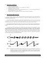
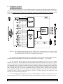
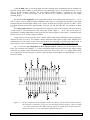
The block diagram presented in Fig. 13 illustrates the entire inner life of the PMC inclusive the
Hand-Control Unit. It shows the functional principle of the PMC electronics and its interaction with the
controls and the analog and digital interface signals.
The complete PMC electronics is supplied by a 35 W switching power supply with a single output
voltage of 12.7 V. All other voltages needed for the electronics (+5 V, ±15 V), including also the variable
bipolar high voltage (±0 V... ±400 V), are generated locally on the printed circuit board via DC/DC
converters.
The positive (+Vs, 0 V... +400 V) and the negative high voltage (-Vs, 0 V... –400 V) are produced by
two high voltage DC/DC converters from the company EMCO. Two separate controller-circuits (HV
Supply Controllers) perform the regulation and the current limitation of each of the two high voltage
DC/DC converters. The set value of the high voltage is wired in parallel to both of the two HV Supply
Controllers, resulting in a symmetrical bipolar high voltage (HV) in a range of ±0 V... ±400 V.
The bipolar HV supply is connected to the HV-Power Stage where the high voltage and high speed
signals are generated and thereafter distributed via the HV-Output Channel Selector to the selected HV
output cannel (HV_out[0..7]).
The HV-Power Stage is a push-pull power stage formed by two high-speed, high-voltage n-channel
MOS-FETs with two high power 22 Ohm resistors in series. These two resistors limit the maximum peakcurrent during the very fast discharge of the load capacitance.
The two gates of the power MOS-FETs are driven by two transformers which perform a galvanic
isolation between the HV power stage and the driving circuit.
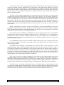
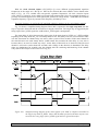
The following explanations are given for a positive sawtooth:
To generate the linear HV ramp, a 1 MHz square wave signal is amplitude modulated and then
transmitted via the transformer to gate of the 'loading' MOS-FET (upper MOS-FET). Thus the
capacitance at the HV output is continuously loaded by a vast series of small 1 MHz current pulses which
result in a fine stepped linear HV ramp at the output. To enable that this principle works for different load
capacitances and independent of the MOS-FET parameters, the linear ramp is generated by using a closed
feedback loop. The amplitude modulation is steered by a PI-Controller which gets the actual value of the
HV output via a Voltage Divider (÷200). The sawtooth reference signal is generated by a multiplying 10
bit DAC connected to a 10 bit counter located inside the PMC-Chip. The analog reference signal of the
multiplying DAC is derived from the actual HV amplitude. This scheme leads to a sawtooth DAC output
signal with an amplitude proportional to the adjusted HV.
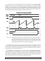
When the linear ramp reaches its maximum positive output voltage (+Vs), a fast back-jump has to
discharges the loaded capacitance to the negative output voltage (-Vs) in a very short time (around 1 μs).
This is performed by an exactly timed discharge pulse feed to the gate of the 'discharge' MOS-FET (lower
MOS-FET). After the fast discharge the HV output voltage is linearly ramped again towards the positive
output voltage (+Vs). A single steps as well as continuous stepping, start and stop with a piezo-motor
output voltage (HV_out ) of zero volt.
For a negative HV ramp (piezo-motor moves in opposite direction) the principle works in the same
way but the functions of the MOS-FETs and some other circuits are swapped.
The complete sawtooth control logic, the relay logic and the computer interface are implemented
inside the PMC-Chip. The PMC-Chip is a programmable CPLD from the company ALTERA.
PMC User's Manual (SP 869)
Physics Basel
Page 18 of 19