1
Freescale Semiconductor
Rev. 0.1, 6/2003
Initializing SDRAM
Parameters for Motorola
MPC106-Based Systems
Freescale Semiconductor, Inc...
This document describes the correlation of the programmable SDRAM interface parameters
of Motorola’s MPC106 PCI bridge/memory controller and typical SDRAM parameters found
in manufacturers’ data sheets. The MPC106 PCI bridge/memory controller provides a
PowerPC™ microprocessor common hardware reference platform (CHRP™) compliant
bridge between the PowerPC microprocessor family and the Peripheral Component
Interconnect (PCI) bus.
Additional information about the topics discussed in this document can be found in MPC106
PCI Bridge/Memory Controller User’s Manual (order #: MPC106UM/AD), and Addendum to
MPC106 PCI Bridge/Memory Controller User’s Manual: MPC106 Revision 4.0 Supplement
and User’s Manual Errata (order #: MPC106UMAD/AD). In this document, the term ‘106’
is used as an abbreviation for, ‘MPC106 PCI bridge/memory controller’.
To locate any published errata or updates for this document, refer to the website at
http://www.mot.com/SPS/PowerPC/.
Note that this document describes the parameters for Rev. 4.0 of the MPC106. Earlier
revisions are slightly different, but the information presented here is applicable with minor
adjustment. For example, Rev. 4.0 has a 10-bit BSTOPRE parameter while Rev. 3.0 has an
8-bit BSTOPRE parameter. This means that while Rev. 4.0 devices can have a
burst-to-precharge interval of 1023 clock cycles, Rev 3.0 devices are restricted to an interval
of 255 clock cycles.
1
SDRAM Interface Parameters
At system reset, initialization software must set up the programmable parameters in the
memory interface configuration registers (MICRs) of the 106. The MICRs control memory
boundaries (starting and ending addresses), memory bank enables, memory buffer control,
and memory controller operation and timing. Initialization software must program the MICRs
at power-on reset and then enable the memory interface on the 106 by setting
MCCR1[MEMGO].
The programmable parameters relevant to the SDRAM interface are:
•
•
•
•
•
© Freesc
Memory bank starting and ending addresses (memory boundary registers)
Memory bank enables (memory bank enable register)
PGMAX—maximum activate-to-precharge interval
SREN—self-refresh enable
RAMTYP—RAM type
conductor, Inc., 2004. All rights reserved.
For More Information On This Product,
Go to: www.freescale.com
Freescale Semiconductor, Inc.
Freescale Semiconductor, Inc...
Programming the Memory Boundary Registers
•
•
•
•
•
•
•
•
•
•
•
•
•
•
•
PCKEN—memory interface parity checking/generation enable
Bank n row—row address bit count for each bank
BSTOPRE[0–9]—burst-to-precharge interval
ECC_EN—ECC enable
REFINT—refresh interval
BUF_MODE—buffer mode
RMW_PAR—read-modify-write parity enable
REFREC—refresh recovery interval
RDLAT—data latency from read command
PRETOACT—precharge-to-activate interval
WCBUF—memory write buffer type
RCBUF—memory read buffer type
ACTOPRE—activate-to-precharge interval
SDMODE—SDRAM mode register
ACTORW—activate-to-read/write interval
The memory interface parameters, SREN, RAMTYP, PCKEN, ECC_EN, BUF_MODE, RMW_PAR,
WCBUF, and RCBUF are governed by the system design (refresh, parity, and buffering) and are not covered
in this document.
2
Programming the Memory Boundary Registers
The extended starting address and the starting address registers are used to define the lower address
boundary for each memory bank. The lower boundary is determined by the following formula:
Lower boundary for bank n = 0b00 || <extended starting address n> || <starting address n> || 0x0 0000
The extended ending address and the ending address registers are used to define the upper address boundary
for each memory bank. The upper boundary is determined by the following formula:
Upper boundary for bank n = 0b00 || <extended ending address n> || <ending address n> || 0xF FFFF
Any unused banks should have their starting and ending addresses programmed out of the range of memory
banks in use. If a disabled bank has its starting and ending address defined as overlapping an enabled bank’s
address space, there may be system memory corruption in the overlapping address range. Therefore, it is
always important to map any unused bank’s starting and ending address to memory space that is not used
by the system.
For example, if a system has one 64-Mbyte bank of SDRAM, in bank 0, starting at address 0x0000_0000
and ending at 0x03FF_FFFF, the memory boundary registers should be programmed as shown in Table 1.
Table 1. Memory Boundary Register Values for 64-Mbyte SDRAM in Bank 0
Value
(Hex)
Address Offset
(Hex)
Memory starting address 1
FFFF_FF00
80
Memory starting address 2
FFFF_FFFF
84
Register
Initializing SDRAM Parameters for Motorola MPC106-Based Systems
For More Information On This Product,
Go to: www.freescale.com
Freescale Semiconductor, Inc.
Programming the Memory Bank Enable Register
Table 1. Memory Boundary Register Values for 64-Mbyte SDRAM in Bank 0 (continued)
Value
(Hex)
Address Offset
(Hex)
Extended memory starting address 1
0303_0300
88
Extended memory starting address 2
0303_0303
8C
Memory ending address 1
FFFF_FF3F
90
Memory ending address 2
FFFF_FFFF
94
Extended memory ending address 1
0303_0300
98
Extended memory ending address 2
0303_0303
9C
Freescale Semiconductor, Inc...
Register
3
Programming the Memory Bank Enable Register
Individual banks are enabled or disabled by using the 1-byte memory bank enable register at address offset
0xA0. If a bank is enabled, the ending address of that bank must be greater than or equal to its starting
address. As stated in the previous section, even if a bank is disabled, its starting and ending addresses must
be programmed to memory space that is not used by enabled banks in the system.
4
Programming the Memory Page Mode Register
The 1-byte memory page mode register at address offset 0xA3 contains the PGMAX parameter, that
controls how long the 106 retains the currently accessed page (row) in memory. The PGMAX parameter
specifies the activate-to-precharge interval (sometimes called row active time or tRAS). The PGMAX value
is multiplied by 64 to generate the actual number of clock cycles for the interval. When PGMAX is
programmed to 0x00, page mode is disabled.
The value for PGMAX depends on the specific SDRAM devices used, the ROM system, and the operating
frequency of the 106. When the interval specified by PGMAX expires, the 106 must close the active page
by issuing a precharge bank command. PGMAX must be sufficiently less than the maximum row active time
for the SDRAM device to ensure that the issuing of a precharge command is not stalled by a memory access.
If a memory access is in progress when PGMAX expires, the 106 must wait for the access to complete
before issuing the precharge command to the SDRAM. In the worst case, the 106 initiates a memory access
one clock cycle before PGMAX expires. If ROM is located on the 60x/memory bus, the longest access that
could potentially stall a precharge is a burst read from ROM. If ROM is located on the PCI bus, then it is
not a factor, and the longest memory access that could potentially stall a precharge is a burst read from the
SDRAM.
The 106 also requires two clock cycles to issue a precharge bank command to the SDRAM device. So, the
PGMAX interval must be further reduced by two clock cycles.
Therefore, PGMAX should be programmed according to the following equation:
PGMAX < [tRAS(MAX) – (worst case memory access) – 2] ÷ 64
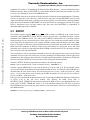
PGMAX parameter settings are shown in Figure 1.
Initializing SDRAM Parameters for Motorola MPC106-Based Systems
For More Information On This Product,
Go to: www.freescale.com
Freescale Semiconductor, Inc.
Programming the Memory Control Configuration Registers
tRAS(MAX) for SDRAM device
PGMAX x 64
Worst case mem access time
2 clocks
Figure 1. PGMAX Parameter Setting for SDRAM Interface
Freescale Semiconductor, Inc...
For example, consider a system with a 60x bus clock frequency of 66 MHz using SDRAMs with a maximum
row active time (tRAS(MAX)) of 100 µs. The maximum number of clock cycles between activate bank and
precharge bank commands is 66 MHz x 100 µs = 6600 clock cycles.
If the system uses 8-bit ROMs on the 60x/memory bus, a burst read from ROM follows the timing shown
in Figure 6-40 in the MPC106 PCI Bridge/Memory Controller User’s Manual. Also affecting the ROM
access time is MCCR2[TS_WAIT_TIMER]. The minimum time allowed for ROM devices to enter high
impedance is two clock cycles. TS_WAIT_TIMER adds clocks (n–1) to the minimum disable time. This
delay is enforced after all ROM accesses preventing any other memory access from starting. Therefore, a
burst read from an 8-bit ROM takes:
{[(ROMFAL + 2) x 8 + 3] x 4 + 5} + [2 + (TS_WAIT_TIMER – 1)] clock cycles
So, if MCCR1[ROMFAL] = 4 and MCCR2[TS_WAIT_TIMER] = 3, the interval for a 60x burst read from
an 8-bit ROM takes:
{[(4 + 2) x 8 + 3] x 4 + 5} + [2 + (3 – 1)] = 209 + 4 = 213 clock cycles
Plugging the values into the PGMAX equation above:
PGMAX < (6600 – 213 – 2) ÷ 64 = 99.7 clock cycles
The value stored in PGMAX should be 0b0110 0011 (or 99 clock cycles).
5
Programming the Memory Control Configuration
Registers
The four 32-bit memory control configuration registers (MCCRs) set all RAM and ROM parameters. These
registers are programmed by initialization software to adapt the 106 to the specific memory organization
used in the system. The following sections describe programming individual SDRAM interface parameters
within the MCCRs. Refer to the MCCR descriptions in Section 1.3.4, “Memory Control Configuration
Registers,” in the Addendum to MPC106 PCI Bridge/Memory Controller User’s Manual and Section
3.2.6.4, “Memory Control Configuration Registers,” in the MPC106 PCI Bridge/Memory Controller User’s
Manual for parameter locations within the MCCRs.
5.1 Bank n Row
Bits 15–0 of MCCR1 determine the row address configuration for the SDRAM devices in banks 0–7 (two
bits per bank). For 64-Mbit devices with four internal banks, MCCR1[Bank n row] should be 0b00. Banks
composed of 64-Mbit devices with two internal banks should have MCCR1[Bank n row] = 0b01. Banks
composed of 16-Mbit devices with two internal banks should have MCCR1[Bank n row] = 0b11.
5.2 BSTOPRE[0–9]
The BSTOPRE parameter is composed of BSTOPRE[0–1] (bits 21–20 of MCCR2), BSTOPRE[2–5] (bits
31–28 of MCCR3), and BSTOPRE[6–9] (bits 3–0 of MCCR4). BSTOPRE controls the burst-to-precharge
interval. BSTOPRE is similar to PGMAX in that when it expires, the 106 must generate a precharge
Initializing SDRAM Parameters for Motorola MPC106-Based Systems
For More Information On This Product,
Go to: www.freescale.com
Freescale Semiconductor, Inc.
Programming the Memory Control Configuration Registers
command. See Section 4, “Programming the Memory Page Mode Register,” for more information on the
PGMAX parameter. However, BSTOPRE is a much shorter duration counter that gets reloaded every time
a read or write command is issued to the SDRAM devices.
The BSTOPRE interval can be optimized for the particular 106-based system implementation. If memory
accesses are typically to the same rows within an active page, then a longer BSTOPRE interval would
improve performance. Alternately, if memory accesses are typically to several locations, spanning multiple
pages, then a shorter duration for BSTOPRE is in order. This allows for a precharge to close the active page
before a subsequent access activates another page. Note that when BSTOPRE is programmed to
0b00 0000 0000, page mode is disabled.
Freescale Semiconductor, Inc...
5.3 REFINT
The memory interface supplies CAS before RAS (CBR) refreshes to SDRAM at the refresh interval
specified by MCCR2[REFINT]. When REFINT expires, the 106 issues a precharge and then a refresh
command to the SDRAM devices. The value stored in REFINT should allow for a potential collision
between memory accesses and refresh cycles. In the worst case, the refresh must wait the number of clock
cycles required by the longest access. For example, if ROM is located on the 60x/memory bus and a ROM
access is in progress at the time a refresh operation needs to be performed, the refresh must wait until the
ROM access has completed. If ROM is located on the 60x/memory bus, the longest access that could
potentially stall a refresh is a burst read from ROM. If ROM is located on the PCI bus, the longest memory
access is a burst read from the SDRAM.
The 106 also has to wait for a precharge command (to close any open pages) before it can issue the refresh
command. The 106 requires two clock cycles to issue a precharge to an internal bank; with two pages open
simultaneously, this equates to four extra clock cycles that must be taken off the refresh interval. Finally, the
106 must wait for the PRETOACT interval to pass before issuing the refresh command.
Therefore, REFINT should be programmed according to the following equation:
REFINT < (per row refresh interval) – (worst case memory access) – (PRETOACT) – 4
Consider a typical SDRAM device with a refresh period of 32 ms for a 2K cycle. This means that it takes
32 ms to refresh each internal bank and each internal bank has 2K rows. To refresh the whole SDRAM (two
internal banks, 4K rows) it takes 64 ms. The refresh time per row is 32 ms ÷ 2048 rows (or 64 ms ÷ 4096
rows) = 15.6 µs. If the 60x bus clock is running at 66 MHz, the number of clock cycles per row refresh is
15.6 µs x 66 MHz = 1030 clock cycles.
If the system uses 8-bit ROMs on the 60x/memory bus, a burst read from ROM will follow the timing shown
in Figure 6–40 in the 106 user’s manual. Also affecting the ROM access time is
MCCR2[TS_WAIT_TIMER]. The minimum time allowed for ROM devices to enter high impedance is two
clock cycles. TS_WAIT_TIMER adds clocks (n–1) to the minimum disable time. This delay is enforced
after all ROM accesses preventing any other memory access from starting. Therefore, a burst read from an
8-bit ROM will take:
{[(ROMFAL + 2) x 8 + 3] x 4 + 5} + [2 + (TS_WAIT_TIMER – 1)] clock cycles
Initializing SDRAM Parameters for Motorola MPC106-Based Systems
For More Information On This Product,
Go to: www.freescale.com
Freescale Semiconductor, Inc.
Programming the Memory Control Configuration Registers
So, if MCCR1[ROMFAL] = 4 and MCCR2[TS_WAIT_TIMER] = 3, the interval for a 60x burst read from
an 8-bit ROM will take:
{[(4 + 2) x 8 + 3] x 4 + 5} + [2 + (3 – 1)] = 209 + 4 = 213 clock cycles
Plugging the values into the REFINT equation above:
REFINT < 1030 – 213 – 2 – 4 = 811 clock cycles
The value stored in REFINT should be 0b00 0011 0010 1010 (or 810 clock cycles).
Freescale Semiconductor, Inc...
5.4 REFREC
REFREC is the refresh recovery interval. This parameter is the number of clock cycles from a refresh
command until a bank activate command is allowed. The interval between a refresh and a new command is
TRC (row cycle time). A typical SDRAM data sheet shows TRC(MIN) = 96 ns. To put this time in clock cycles,
for a 66-MHz bus, 96 ns x 66 MHz = 6.3 clock cycles. Rounding up to 7, the value stored to REFREC should
be 0b0111.
5.5 RDLAT
RDLAT is the data latency from a read command. This parameter controls the number of clock cycles from
a read command until the first data beat is valid on the 60x data bus. The read command is issued with the
assertion of SDCAS. Therefore, this parameter equates to the CAS latency (TCAC) plus whatever latency is
imposed by the data buffers. Note that data latency is programmable for read operations (RDLAT). For write
operations, the first valid data beat coincides with the SDRAM write command.
A typical SDRAM data sheet says that CAS latency is 30 ns. To put this time in clock cycles, for a 66-MHz
bus, 30 ns x 66 MHz = 1.98 clock cycles (rounding up, 2 clock cycles). If the system uses registered data
buffers, there is a one clock delay between data valid on the memory bus and data valid on the 60x bus, so
the value stored to RDLAT should be 2 + 1 = 3 clock cycles (0b0011).
5.6 PRETOACT
PRETOACT is the number of clock cycles from a precharge command until a bank activate command is
allowed.
A typical SDRAM data sheet shows that TRP is the minimum row precharge time. That is, the time after a
precharge command is issued before the bank activate command can begin. TRP for a typical SDRAM
device is 30 ns. To put this time in clock cycles, for a 66-MHz bus, 30 ns x 66 MHz = 1.98 clock cycles.
Rounding up to 2, the value stored to PRETOACT should be 0b0010.
5.7 ACTOPRE
ACTOPRE is the number of clock cycles from a bank activate command until a precharge command is
allowed.
In a typical SDRAM data sheet, TRAS(MIN) is the specification for minimum row active time. Every bank
activate command must satisfy the TRAS(MIN) specification before a precharge command can be issued to
that active bank.
For a typical SDRAM device, TRAS(MIN) is 70 ns. To put this time in clock cycles, for a 66-MHz bus,
70 ns x 66 MHz = 4.62 clock cycles. Rounding up to 5, the value stored to ACTOPRE should be 0b0101.
Initializing SDRAM Parameters for Motorola MPC106-Based Systems
For More Information On This Product,
Go to: www.freescale.com
Freescale Semiconductor, Inc.
Revision History
5.8 SDMODE
SDMODE specifies the SDRAM mode register data to be written to the SDRAM array during power-up
configuration. The 106 has certain restrictions for the SDMODE bits. In fact, the only variable in the
SDMODE fields is the CAS latency parameter.
The opcode should be 0b0 0000 for normal operation.
In a typical SDRAM data sheet, TCAC is the specification for CAS latency. TCAC is programmable on most
SDRAM devices to one, two, or three clock cycles depending on operating frequency of the device. A
typical SDRAM data sheet says that CAS latency is 30 ns. To put this time in clock cycles, for a 66-MHz
bus, 30 ns x 66 MHz = 1.98 clock cycles. Rounding up to 2, the value for CAS latency should be 0b0010.
Freescale Semiconductor, Inc...
Finally, the wrap type must be 0b0 for sequential type wrapping and the wrap length must be 0b010 for four
(doubleword) beats for each access.
Therefore, the complete value stored to SDMODE should be 0b0000 0010 0010.
Note that for 64-Mbit SDRAMs, the SDRAM mode register data is actually a 14-bit field. On the 106, the
two-most-significant bits are forced to 0 and concatenated to MCCR4[SDMODE].
5.9 ACTORW
ACTORW controls the number of clocks cycles from a bank activate command until a read or write
command is allowed. It must be at least two clock cycles.
In a typical SDRAM data sheet, TRCD is the specification for the RAS-to-CAS delay time. For SDRAM
command encodings, RAS corresponds to the bank activate command and CAS corresponds to the read or
write command.
For a typical SDRAM device, TRCD = 25 ns. To put this time in clock cycles, for a 66-MHz bus,
25 ns x 66 MHz = 1.65 clock cycles. Rounding up to 2, the value for ACTORW should be 0b0010.
6
Revision History
Table 2 shows the revision history of this document.
Table 2. Revision History
Revision
Number
Changes
0.0
Initial release
0.1
Nontechnical reformatting
Initializing SDRAM Parameters for Motorola MPC106-Based Systems
For More Information On This Product,
Go to: www.freescale.com
Freescale Semiconductor, Inc.
How to Reach Us:
Home Page:
www.freescale.com
Freescale Semiconductor, Inc...
E-mail:
[email protected]
USA/Europe or Locations Not Listed:
Freescale Semiconductor
Technical Information Center, CH370
1300 N. Alma School Road
Chandler, Arizona 85224
+1-800-521-6274 or +1-480-768-2130
[email protected]
Europe, Middle East, and Africa:
Freescale Halbleiter Deutschland GmbH
Technical Information Center
Schatzbogen 7
81829 Muenchen, Germany
+44 1296 380 456 (English)
+46 8 52200080 (English)
+49 89 92103 559 (German)
+33 1 69 35 48 48 (French)
[email protected]
Japan:
Freescale Semiconductor Japan Ltd.
Headquarters
ARCO Tower 15F
1-8-1, Shimo-Meguro, Meguro-ku,
Tokyo 153-0064
Japan
0120 191014 or +81 3 5437 9125
[email protected]
Asia/Pacific:
Freescale Semiconductor Hong Kong Ltd.
Technical Information Center
2 Dai King Street
Tai Po Industrial Estate
Tai Po, N.T., Hong Kong
+800 2666 8080
[email protected]
For Literature Requests Only:
Freescale Semiconductor Literature Distribution Center
P.O. Box 5405
Denver, Colorado 80217
1-800-441-2447 or 303-675-2140
Fax: 303-675-2150
[email protected]
Information in this document is provided solely to enable system and software
implementers to use Freescale Semiconductor products. There are no express or
implied copyright licenses granted hereunder to design or fabricate any integrated
circuits or integrated circuits based on the information in this document.
Freescale Semiconductor reserves the right to make changes without further notice to
any products herein. Freescale Semiconductor makes no warranty, representation or
guarantee regarding the suitability of its products for any particular purpose, nor does
Freescale Semiconductor assume any liability arising out of the application or use of
any product or circuit, and specifically disclaims any and all liability, including without
limitation consequential or incidental damages. “Typical” parameters which may be
provided in Freescale Semiconductor data sheets and/or specifications can and do
vary in different applications and actual performance may vary over time. All operating
parameters, including “Typicals” must be validated for each customer application by
customer’s technical experts. Freescale Semiconductor does not convey any license
under its patent rights nor the rights of others. Freescale Semiconductor products are
not designed, intended, or authorized for use as components in systems intended for
surgical implant into the body, or other applications intended to support or sustain life,
or for any other application in which the failure of the Freescale Semiconductor product
could create a situation where personal injury or death may occur. Should Buyer
purchase or use Freescale Semiconductor products for any such unintended or
unauthorized application, Buyer shall indemnify and hold Freescale Semiconductor
and its officers, employees, subsidiaries, affiliates, and distributors harmless against all
claims, costs, damages, and expenses, and reasonable attorney fees arising out of,
directly or indirectly, any claim of personal injury or death associated with such
unintended or unauthorized use, even if such claim alleges that Freescale
Semiconductor was negligent regarding the design or manufacture of the part.
AN1725/D
For More Information On This Product,
Go to: www.freescale.com