1
CHAPTER 4 DIFFERENCES BETWEEN TARGET INTERFACE CIRCUIT AND TARGET DEVICE
4.2
For 78K0/FE2 Emulation
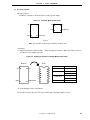
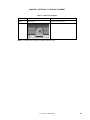
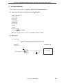
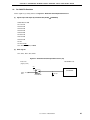
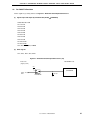
For the signals in (1) and (2) below, see Figure 4-2 Emulation Circuit Equivalent Circuit 2.
(1) Signals input and output by emulation CPU (FPGA, μ PD78F0893)
• P06, P05, 01, P00
• P17 to P10
• P33 to P30
• P43 to P40
• P53 to P50
• P63 to P60
• P76 to P70
• P87 to P80
• P93 to P90
• P120
• P132 to P130
• X2, XT2, RESET, VSS, FLMD0
(2) Other signals
• VDD, EVSS, EVDD, AVSS, AVREF
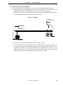
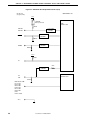
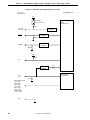
Figure 4-2. Emulation Circuit Equivalent Circuit 2 (1/2)
• Probe side
(target system)
• QB-78K0FX2 side
VDD
AVREF, VDD,
EVDD
μ PD78F0893
PI5A4624TX
0.1 μF
User’s Manual U17669EJ3V0UM
35