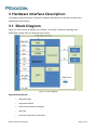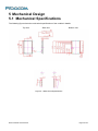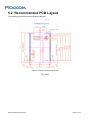
1
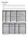
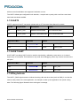
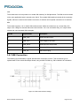
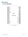
3.8.2 SIM Design Guidelines The SIM interface and signals design is extremely important for proper operation of module and the SIM card. There are several design guidelines that must be followed to achieve a robust and stable design that meets the required standards and regulations. The SIM should be located, and its signals should be routed, away from any possible EMI sources, such as the RF antenna and digital switching signals. The SIM interface signals length should not exceed 100 mm between the module interface connector and the SIM tray. This is to meet with EMC regulations and improve signal integrity. To avoid crosstalk between the SIM clock and data signals (SIM_CLK and SIM_DATA), it is recommended to rout them separately on the application board, and preferably isolated by a surrounding ground plane. The SIM card signals should be protected from ESD using very low capacitance protective elements (zener diodes, etc.). The recommended part no of ESD isAVR-M1005C270MAAB (TDK) We also recommended the ESD component should layout with SIM hold closely. 3.9 I2C Interface G610 supports I2C interface, two lines: one serial data line SDA, one serial clock line SCL. Features: Reaches up to 400kbit/s Open drain output Generate start bit and stop bit automatically Response and confirm automatically Application hardware I2C protocol Pin No. Signal Name Description 36 SDA/GPIO19 I2C data signal 37 SCL/GPIO18 I2C clock signal Note: If the customer needs this function, please adjust the software based on the specific device. G610 Hardware User Manual Page 26 of 41