1
User Manual
STM32F2/4
Evaluation Board
Introduction
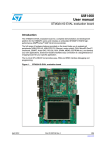
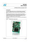
The STM32F417IGH6 evaluation board
STM32F2/4-EVB is designed as complete
development platform for STMicroelectronic’s
ARM Cortex-M3 core-based STM32F417IGH6
microcontroller with digital camera module
interface, High speed USB OTG, Full speed
USB OTG, Ethernet MAC, FSMC interface,
two channels of CAN2.0A/B compliant interface,
2channels I2S, 3 channels I2C, 6 channels
USART with smart card support, 3 channels
SPI, SDIO, 3 ADC, 2 DAC, internal 128KB
SRAM and 1MB Flash, JTAG&SWD debugging
support. The full range of hardware features
on the board is able to help you evaluate all
peripherals (USB OTG HS, USB OTG FS,
Ethernet, CAN, SD card, Smart card, USART, Audio DAC, RS232, PSRAM,NAND, MEMS,
EEPROM… etc.) and develop your own applications. Extension headers make it possible to
easily connect a daughter board or wrapping board for your specific application.
Features
■
Four 5V power supply options: Power jack, USB FS connector, USB HS connector or
daughter board.
■
Boot from User Flash, System memory or SRAM.
■
I2S Audio DAC, stereo audio jack.
■
1GByte or more SD card.
■
Both type A&B Smart card support.
■
I2C compatible serial interface 64KBit EEPROM, MEMS .
■
RS232 communication.
■
IrDA transceiver.
■
USB OTG HS and FS with Micro-AB connector.
■
IEEE-802.3-2002 compliant Ethernet connector.
■
Camera module
■
4Mbit PSRAM
■
512Mbit NAND
■
Two channels of CAN2.0A/B compliant connection.
■
Inductor Motor Control connector.
■
JTAG ,SW and Trace Debug support.
■
3.2” 240x400 TFT color LCD with touch screen.
■
Joystick with 4-direction control and selector.
■
Reset, Wakeup, Tamper and User button.
■
4 color LEDs.
■
RTC with backup battery.
■
Extension connector for daughter board or wrapping board.
Contents
1. Hardware Layout and configuration ....................................................................................5
1.1 Power Supply ....................................................................................................................7
1.2 Boot Option .......................................................................................................................8
1.3 Clock Source......................................................................................................................8
1.4 Reset Source.....................................................................................................................9
1.5 Audio .................................................................................................................................9
1.6 EEPROM...........................................................................................................................9
1.7 CAN...................................................................................................................................9
1.8 RS232 .............................................................................................................................10
1.9 SD card.......................................................................................................................... 10
1.10 MEMS............................................................................................................................11
1.11 USB OTG FS............................................................................................................... 11
1.12 Ethernet....................................................................................................................... 11
1.13 USB OTG HS
.............................................................................................................11
1.14 Camera Module........................................................................................................... 12
1.15 PSRAM and NAND
……........................................................................................... 12
1.16 Development and Debug support ............................................................................... 12
1.17 Display and Input devices ........................................................................................... 12
2. Connector .........................................................................................................................13
2.1 Daughter board extension connector CN1, 2, 3 and CN4............................................. 17
2.2 SD connector CN5
.......................................................................................................19
2.3 Ethernet RJ45 connector CN7
.....................................................................................20
2.4 USB OTG FS MINI-B connector CN12 …………………………………………………….20
2.5 USB OTG HS MINI-B connector CN13 ..........................................................................21
2.6 CAN D-type 9-pins male connector CON4(CAN2) & CON2(CAN1) ..............................21
2.7 Audio connector CN11 ...................................................................................................22
2.8 JTAG debugging connector CN8.. .................................................................................22
2.9 Camera module connector CN10................................................................................. 23
2.10 RS232 connector CON1&CON5...................................................................................24
2.11 RS232 connector CON3.. ............................................................................................24
2.12 Power connector CN6.. ................................................................................................25
2.13 TFT LCD connector CN9..............................................................................................25
3. Schematic ........................................................................................................................27
1. Hardware Layout and configuration
The STM32F2/4-EVB evaluation board is designed around the STM32F417IGH6 in 176-pin
UFBGA package. The hardware block diagram Figure 2 illustrates the connection between
STM32F417IGH6 and peripherals (Camera module, LCD, PSRAM, NAND, EEPROM, MEMS,
USART, USB OTG HS, USB OTG FS, Ethernet, Audio, CAN bus, SD card ) and Figure 3 will
help you locate these features on the actual evaluation board.
Figure 2: Hardware Block Diagram
BLOCK DIAGRAM
USB POWER
SWITCH
3.3V REGULATOR
OTG HS
2.5V REGULATOR
MCU
CONSUMPTION
MEASUREMENT
DAC
AUDIO DAC
GPIO
FSMC
TFT LCD
SD CARD
DB9
CONNECTOR
DB9
CONNECTOR
DB9
CONNECTOR
MEMS
EEPROM
STM32F417IGH6
NAND
PSRAM
USB
CONNECTOR
I2S
I2C1
LED,KEY
USB HS
PHY
DCMI
CAMERA
MODULE
USB
CONNECTOR
OTG FS
SDIO
JTAG/SWD
DEBUG
RS232
TRANSCEIVER
UART1
RS232
TRANSCEIVER
UART2
USB POWER
SWITCH
MII/RMII
CAN1
UART3
CAN2
PHY
RJ45
CONNECTOR
CAN
TRANSCEIVER
DB9
CONNECTOR
CAN
TRANSCEIVER
DB9
CONNECTOR
Figure 3: STM32F2/4-EVB Evaluation board layout
1.1 Power Supply
STM32F2/4-EVB evaluation board is designed to be powered by 5V DC power supply and to
be protected by PolyZen from wrong power plug-in event. It’s possible to configure the
evaluation board to use any of following Four sources for the power supply.
■
5V DC power adapter connected to CN6, the Power Jack on the board (PSU on silk screen
for Power Supply Unit).
■
5V DC power with 500mA limitation from CN12, the USB OTG FS Mini-B connector (FS on
silkscreen).
■
5V DC power with 500mA limitation from CN13, the USB OTG HS Mini-B connector (HS on
silkscreen).
The power supply is configured by setting the related jumpers JP1,JP7 as described in table 1.
Table 1 Power related Jumpers
JUMPER
Description
JP1 is used to select one of the four possible power supply resources.
For power supply jack(CN6) to the STM32F2/4-EVB only, JP1 is set as shown
to the right:
(Default Setting)
J1
PSU
FS
HS
●
●
●
●
●
●
For power supply from USB OTG FS (CN12) to STM32F2/4-EVB only,
JP1 is set as shown to the right:
J1
JP1
PSU
FS
HS
●
●
●
●
●
●
For power supply from USB OTG HS (CN13) to STM32F2/4-EVB only,
JP1 is set as shown to the right:
J1
PSU
FS
HS
●
●
●
●
●
●
Vbat is connected to battery when JP1 is set as shown to the right:
1
2
3
● ● ●
JP7
Vbat is connected to 3.3V power when JP1 is set as shown to the right:
(Default setting)
1
2 3
● ● ●
The LED D9 is lit when the STM32F2/4-EVB evaluation board is powered by the 5V correctly.
1.2 Boot Option
The STM32F2/4-EVB evaluation board is able to boot from:
■
Embedded User Flash
■
System memory with boot loader for ISP
■
Embedded SRAM for debugging
The boot option is configured by setting switch SW1 (BOOT1) and SW2 (BOOT0).
Table 2 Boot related Switch
BOOT0
0
BOOT1
X
Boot from
JP3
JP4
BOOT0
BOOT1
STM32F2/4-EVB boot from User Flash when
1
2
3
BOOT0 is set as shown to the right. BOOT1 is
● ● ●
● ● ●
STM32F2/4-EVB boot from System Memory
1
1
when BOOT0 and BOOT1 are set as shown to
● ● ●
● ● ●
STM32F2/4-EVB boot from Embedded
1
1
SRAM when BOOT0 and BOOT1 are set as
● ● ●
1
2
3
don’t care in this configuration.
(Default setting)
1
0
2
3
2
3
the right.
1
1
2
3
2
3
● ● ●
shown to the right.
1.3 Clock Source
Four clock sources are available on STM32F2/4-EVB evaluation board for STM32F417IGH6
and RTC embedded.
■
Y2, 25MHz Crystal for Ethernet PHY.
■
Y3, 24MHz Crystal for USB OTG HS PHY.
■
X1, 32KHz Crystal for embedded RTC.
■
Y1, 25MHz Crystal with socket for STM32F417IGH6 Microcontroller, it can be removed
when internal RC clock is used.
1.4 Reset Source
The reset signal of STM32F2/4-EVB evaluation board is low active and the reset sources
include:
■
Reset button SW1
■
Debugging Tools from JTAG connector CN8.
■
Daughter board from CN2
1.5 Audio
STM32F2/4-EVB evaluation board supports stereo audio play thanks to an audio DAC
CS43L22 connected to both I2S2 port and one channels of DAC of microcontroller
STM32F417IGH6. The CS43L22 can be configured via I2C1. The automatically switch
between the speaker and headphone is supported by both CS43L22 and audio jack with plug
detection pin.
1.6 EEPROM
A 64KBit EEPROM connected to I2C1 bus of STM32F417IGH6.
1.7 CAN
STM32F2/4-EVB evaluation board supports two channels of CAN2.0A/B complaint CAN bus
communication based on 3.3V CAN transceiver. The two CAN bus are disabled and
disconnected by jumpers from relevant STM32F417IGH6 IO’s CAN2 is shared with USB OTG
HS. The switch must be re-set to enable CAN2 as listed in table 6 and table 7.
Table 3 CAN1 related Jumpers
Jumper
Description
JP8
CAN1 terminal resistor is enabled when JP8 is fitted.
Default setting: Not fitted
Table 4 CAN2 related Jumpers
Jumper
Description
JP9
CAN2 terminal resistor is enabled when JP9 is fitted.
Default setting: Not fitted
SW5-7
CAN2_TX is connected to PB13 and USB OTG HS is disabled(SW5-8 OFF)
Default setting: Not fitted
SW5-5
CAN2_RX is connected to PB5 and USB OTG HS is disabled(SW5-6 OFF)
Default setting: Not fitted
1.8 RS232
RS232 communication is supported by D-type 9-pins RS232 connectors CON1(UART1) ,
CON3(UART2) , CON5(UART3) which are connected of STM32F417IGH6 on
STM32F2/4-EVB evaluation board.
RS232 can be selected by setting of SW2,SW3,SW5:
Table 5 RS232 Related Switch
UART1: ( shared with USB FS)
Switch_ ON
Description
SW3-1
UART1_TX is connected to PA9 and USB OTG FS is disabled(SW3-2 OFF)
Default setting: Not fitted
SW3-3
UART1_RX is connected to PA10 and USB OTG FS is disabled(SW3-4
OFF)
Default setting: Not fitted
UART2:( shared with USB HS & ETHERNET)
Switch_ ON
Description
SW2-1
UART2_CTS is connected to PA0 and WAKE is disabled(SW2-2 OFF)
Default setting: Not fitted
SW2-3
UART2_RTS is connected to PA1 and ETHERNET is disabled(SW2-4 OFF)
Default setting: Not fitted
SW2-5
UART2_TX is connected to PA2 and ETHERNET is disabled(SW2-6 OFF)
Default setting: Not fitted
SW2-7
UART2_RX is connected to PA3 and USB OTG HS is disabled(SW2-8 OFF)
Default setting: Not fitted
UART3:( shared with USB HS)
Switch_ ON
Description
SW5-1
UART3_TX is connected to PB10 and USB OTG HS is is disabled(SW5-2
OFF)
Default setting: Not fitted
SW5-3
UART3_RX is connected to PB11 and USB OTG HS is is disabled(SW5-4
OFF)
Default setting: Not fitted
1.9 MicroSD card
The 1GByte or more MicroSD card connected to SDIO of STM32F417IFT6 is available on the
board. MicroSD card Detection is managed by standard IO port PF11.
1.10 MEMS
A ST MEMS device LIS3DH is connected to I2C1 bus of STM32F417IGH6 on the board.
1.11 USB OTG FS
STM32F2/4-EVB evaluation board support USB OTG full speed communication via a USB
MINI-B connector (CN12) and USB power switch (JP7) connected to VBUS. The evaluation
board can be powered by this USB connection at 5V DC with 500mA current limitation.
1.12 Ethernet
STM32F2/4-EVB evaluation board support 10M/100M Ethernet communication by a PHY
IP101A (U7) and integrated RJ45 connector (CN7). Both MII and RMII interface mode are
supported and can be selected by setting of Jumper JP6 and Switch SW2 as listed below:
Table 6 Ethernet Related Jumpers
Jumper
Description
25MHz clock is provided by external crystal X1 (for MII interface mode only)
when JP6 is set as shown to the right:
1
2
3
● ● ●
JP6
25MHz clock for MII or 50MHz clock for RMII is provided by MCO when JP6 is
set as shown to the right (Default setting):
1
2
3
● ● ●
Table 7 Ethernet Related Switch(shared with UART2)
Switch_ ON
Description
ETH_RX_CLK is connected to PA1 and USART2_RTS
SW2-4
is disabled(SW2-3
OFF)
Default setting: fitted
SW2-6
ETH_MDIO is connected to PA2 and USART2_TX is disabled(SW2-5 OFF)
Default setting: fitted
1.13 USB OTG HS
STM32F2/4-EVB evaluation board support USB OTG High speed communication via a USB
Mini-B connector (CN13), USB High speed PHY (U19) and USB power switch (U18)
connected to VBUS. The evaluation board can be powered by this USB connector (CN13) at
5V DC with 500mA current limitation.
The USB ULPI bus is shared with UART2,MEMS,SPI1,UART3,CAN2,the SW2~SW5 must be
serring for USB OTG HS.
Table 8 Ethernet Related Switch(shared with UART2,MEMS,SPI1,UART3,CAN2)
Switch_ON
Description
ULPI_D0 is connected to PA3 and USART2_RX is disabled(SW2-7 OFF)
SW2-8
Default setting: fitted
ULPI_D1 is connected to PB0 and MEMS_INT1is disabled(SW3-5 OFF)
SW3-6
Default setting: fitted
ULPI_D2 is connected to PB1 and MEMS_INT2is disabled(SW3-7 OFF)
SW3-8
Default setting: fitted
ULPI_D7 is connected to PB5 and SPI1_MOSI is disabled(SW4-7 OFF)
SW4-8
Default setting: fitted
ULPI_D3 is connected to PB10 and USART3_TX is disabled(SW5-1 OFF)
SW5-2
Default setting: fitted
ULPI_D4 is connected to PB11 and USART3_RX is disabled(SW5-3 OFF)
SW5-4
Default setting: fitted
ULPI_D5 is connected to PB12 and CAN2_RX is disabled(SW5-5 OFF)
SW5-6
Default setting: fitted
ULPI_D6 is connected to PB13 and CAN2_TX is disabled(SW5-7 OFF)
SW5-8
Default setting: fitted
1.14 Camera Module
Camera module is connected to DCMI bus of STM32F417IGH6.
1.15 PSRAM and NAND
The 4Mbit PSRAM and 512Mbit NAND are connected to FSMC bus of STM32F417IGH6.
1.16 Development and Debug support
The two debug connectors available on STM32F2/4-EVB evaluation board are:
1. CN8, standard 20-pins JTAG interface connector that is compliant with debug tools of
ARM7 and ARM9.
2. 1.17 Display and Input devices
The 3.2” TFT color LCD connected to FSMC bus and 4 general purpose color LED’s
(D10,11,12,13) are available as display device. A touch screen connected to TSC2007,
direction joystick with selection key, general purpose button (SW9), Wakeup button (SW10)
and Tamper detection button (SW8) are available as input devices.
Table 9 LCD modules(TFT LCD with touch screen (CN9))
Pin on
Pin name
Pin connection
CN16
1
Pin on
Pin name
Pin connection
RS
FSMC_A0(PF0)
CN16
CS
FSMC_NE3 (PG10)
2
3
WR/SCL
FSMC_NWE(PD5)
4
RD
FSMC_NOE(PD4)
5
RESET
RESET#
6
PD0
FSMC_D0(PD14)
7
PD1
FSMC_D1(PD15)
8
PD2
FSMC_D2(PD0)
9
PD3
FSMC_D3(PD1)
10
PD4
FSMC_D4(PE7)
11
PD5
FSMC_D5(PE8)
12
PD6
FSMC_D6(PE9)
13
PD7
FSMC_D7(PE10)
14
PD8
FSMC_D8(PE11)
15
PD9
FSMC_D9(PE12)
16
PD10
FSMC_D10(PE13)
17
PD11
FSMC_D11(PE14)
18
PD12
FSMC_D12(PE15)
19
PD13
FSMC_D13(PD8)
20
PD14
FSMC_D14(PD9)
21
PD15
FSMC_D15(PD10)
22
BL_GND
GND
23
BL_CONTR
+5V
24
VDD
+3.3V
OL
25
VCI
+3.3V
26
GND
GND
27
GND
GND
28
BL_VDD
+5V
29
SDO
SDO(PB6)
30
SDI
SDI(PB9)
31
XL
XL
32
XR
XR
33
YD
YD
34
YU
YU
2. Connector
2.1 Daughter board extension connector CN1,2,3 and CN4
Four male headers CN1,2,3 and CN4 can be used to connect with daughter board or
standard wrapping board to STM32F2/4-EVB evaluation board. All total 140 GPI/Os are
available on it.
Table 10 Daughter board extension connector CN2
Pin
Description
Alternative Function
1
PE2
FSMC_A23
2
PE3
FSMC_A19
3
PE4
FSMC_A20
4
PE5
FSMC_A21
5
PE6
FSMC_A22
6
VBAT
--
7
PI8-RTC_AF2
GPIO(KEY)
8
PC13-RTC_AF1
GPIO(TAMPER)
9
PC14-OSC32_IN
OSC32_IN
10
PC15-OSC32_OUT
OSC32_OUT
11
PI9
CAN1_RX
12
PI10
ETH_RX_ER
13
PI11
ULPI_DIR
14
VSS-14
GND
15
VDD_14
VCC
16
PF0
FSMC_A0
17
PF1
FSMC_A1
18
PF2
FSMC_A2
19
PF3
FSMC_A3
20
PF4
FSMC_A4
21
PF5
FSMC_A5
22
VSS_5
GND
23
VDD_5
VCC
24
PF6
GPIO(SDC_WP)
25
PF7
GPIO(K_UP/LED1)Change form SW6
26
PF8
GPIO(K_LEFT/LED2)Change form SW6
27
PF9
GPIO(K_RIGHT/LED3)Change form SW6
28
PF10
GPIO(K_DOWN/LED4)Change form SW6
29
PH0-OSC_IN
OSC_IN(25MHz)
30
PH1-OSC_OUT
OSC_OUT(25MHz)
31
NRST
CPU Reset(LOW Reset)
31
PC0
ULPI_STP
33
PC1
ETH_MDC
34
PC2
ETH_TXD2
35
PC3
ETH_TX_CLK
36
VDD_12
VDD
37
VSSA
GND
38
VREF+
VREF+
39
VDDA
VDDA
40
PA0-WKUP
WAKE/USART2_CTS(Change form SW2)
41
PA1
ETH_RX_CLK/USART2_RTS(Change form SW2)
42
PA2
ETH_MDIO/USART2_TX(Change form SW2)
43
PH2
ETH_CRS
44
PH3
ETH_COL
Table 11 Daughter board extension connector CN3
Pin
Description
Alternative Function
45
PH4
ULPI_NXT
46
PH5
----
47
PA3
ULPI_D2/USART2/RX(Change form SW2)
48
VSS_4
GND
49
VDD_4
VCC
50
PA4
AUDIO_DAC
51
PA5
ULPI_CLK
52
PA6
CAM_PCLK
53
PA7
ETH_RX_DV
54
PC4
ETH_RXD0
55
PC5
ETH_RXD1
56
PB0
ULPI_D1/MEMS_INT1(Change form SW3)
57
PB1
ULPI_D2/MEMS_INT2(Change form SW3)
58
PB2
GPIO(TOUCH_INT)
59
PF11
GPIO(SD_RDY)
60
PF12
FSMC_A6
61
VSS_6
GND
62
VDD_6
VCC
63
PF13
FSMC_A7
64
PF14
FSMC_A8
65
PF15
FSMC_A9
66
PG0
FSMC_A10
67
PG1
FSMC_A11
68
PE7
FSMC_D4
69
PE8
FSMC_D5
70
PE9
FSMC_D6
71
VSS_7
GND
72
VDD_7
VCC
73
PE10
FSMC_D7
74
PE11
FSMC_D8
75
PE12
FSMC_D9
76
PB13
FSMC_D10
77
PE14
FSMC_D11
78
PE15
FSMC_D12
79
PB10
ULPI_D3/USART3_TX(Change form SW5)
80
PB11
ULPI_D4/USART3_RX(Change form SW5)
81
VCAP1
VCAP1
82
VDD_1
VCC
83
PH6
ETH_RXD2
84
PH7
ETH_RXD3
85
PH8
CAM_HSYNC
86
PH9
CAM_DATA0
87
PH10
CAM_DATA1
88
PH11
CAM_DATA2
Table 12 Daughter board extension connector CN4
Pin
Description
Alternative Function
89
PH12
CAM_DATA3
90
VSS_14
GND
91
VDD_14
VCC
92
PB12
ULPI_D5/CAN2_RX(Change form SW5)
93
PB13
ULPI_D6/CAN2_TX(Change form SW5)
94
PB14
GPIO(LCDBKL_CTL)
95
PB15
GPIO(K_SEL)
96
PD8
FSMC_D13
97
PD9
FSMC_D14
98
PD10
FSMC_D15
99
PD11
FSMC_A16
100
PD12
FSMC_A17
101
PD13
FSMC_A18
102
VSS_8
GND
103
VDD_8
VCC
104
PD14
FSMC_D0
105
PD15
FSMC_D1
106
PG2
FSMC_A12
107
PG3
FSMC_A13
108
PG4
FSMC_A14
109
PG5
FSMC_A15
110
PG6
FSMC_INT2
111
PG7
ZIGBEE_WAKE
112
PG8
ZIGBEE_INT
113
VSS_9
GND
114
VDD_9
VCC
115
PC6
I2S_MCK
116
PC7
----
117
PC8
SDC_D0
118
PC9
SDC_D1
119
PA8
ETH_MCO
120
PA9
USB_FS_DETECT/UART1_TX(Change form SW3)
121
PA10
USB_FS_ID/UART1_RX(Change form SW3)
122
PA11
USB_FS_DN
123
PA12
USB_FS_DP
124
PA13
JTMS
125
VCAP2
VCAP2
126
VSS_2
GND
127
VDD_2
VCC
128
PH13
CAN1_TX
129
PH14
CAM_DATA4
130
PH15
----
131
PI0
I2S_CMD
132
PI1
I2S_CLK
Table 13 Daughter board extension connector CN1
Pin
Description
Alternative Function
133
PI2
TOUCH_INT
134
PI3
I2S_DIN
135
VSS_15
GND
136
VDD_15
VCC
137
PA14
JTCK
138
PA15
JTDI/SPI1_NSS(Change form SW4)
139
PC10
SDC_D2
140
PC11
SDC_D3
141
PC12
SDC_CLK
142
PD0
FSMC_D2
143
PD1
FSMC_D3
144
PD2
SDC_CMD
145
PD3
FSMC_CLK
146
PD4
FSMC_NOE
147
PD5
FSMC_NWE
148
VSS_10
GND
149
VDD_10
VCC
150
PD6
FSMC_NWAIT
151
PD7
FSMC_NE1
152
PG9
FSMC_NE2
153
PG10
FSMC_NE3
154
PG11
ETH_TX_EN
155
PG12
----
156
PG13
ETH_TXD0
157
PG14
ETH_TXD1
158
VSS_11
GND
159
VDD_11
VCC
160
PG15
----
161
PB3
JTDO/SPI1_SCK(Change form SW4)
162
PB4
JTRST/SPI1_MISO(Change form SW4)
163
PB5
ULPI_D7/SPI1_MISO(Change form SW4)
164
PB6
I2C1_SCL
165
PB7
FSMC_NL
166
BOOT0
BOOT0
167
PB8
ETH_TXD3
168
PB9
I2C1_SDA
169
PE0
FSMC_NBL0
170
PE1
FSMC_NBL1
171
RFU
Reserved
172
VDD_3
VCC
173
PI4
CAM_DATA5
174
PI5
CAM_VSYNC
175
PI6
CAM_DATA6
176
PI7
CAM_DATA7
2.2 SD connector CN5
Figure 4 SD connector CN5
Table 14 SD connector CN5
Pin number
Description
Pin name
1
SDC_D3
PC11
2
SDC_CMD
PD2
3
VSS
4
VDD
5
SDC_CLK
6
VSS
7
SDC_D0
PC8
8
SDC_D1
PC9
9
SDC_D2
PC10
CD
SD_RDY
PF11
WP
SDC_WP
PF6
PC12
2.3 Ethernet RJ45 connector CN7
Figure 5 Ethernet RJ45 connector CN7
Pin number
Description
1
TxData+
2
TxData-
3
RxData+
4
Shield
5
Shield
6
RxData-
7
Shield
8
Shield
2.4 USB OTG FS MINI-AB connector CN12
Figure 6 USB OTG FS MINI-B connector CN12
Pin number
Description
1
VBUS (PA9)
2
D- (PA11)
3
D+ (PA12)
4
ID (PA10)
5
GND
2.5 USB OTG HS MINI-B connector CN13
Figure 7 USB OTG HS Micro-AB connector CN9
Pin number
Description
1
VBUS
2
D-
3
D+
4
ID
5
GND
2.6 CAN D-type 9-pins male connector CON4(CAN2) &
CON2(CAN1)
Figure 8 CAN D-type 9-pins male connector CON4 (CAN2) & CON2 (CAN1)
Table 15 CAN D-type 9-pins male connector CON4 (CAN2) & CON2(CAN1)
Pin number
Description
1,4,8,9
NC
2
CANL
7
CANH
3,5,6
GND
2.7 Audio connector CN11
A 3.5mm Stereo audio jack CN11 with plug-detection feature connected to audio DAC is
available on STM32F2/4-EVB board.
2.8 JTAG debugging connector CN8
Figure 9 JTAG debugging connector CN8
Table 16 JTAG debugging connector CN8
Pin number
Description
Pin number
Description
1
3.3V power
2
3.3V power
3
JTRST/PB4
4
GND
5
JTDI/PA15
6
GND
7
JTMS/PA13
8
GND
9
JTCK/PA14
10
GND
11
RTCK
12
GND
13
JTDO/PB3
14
GND
15
RESET#
16
GND
17
DBGRQ
18
GND
19
DBGACK
20
GND
2.9 Camera module connector CN10
Figure 10 Camera module connector CN10
Table 17 Camera module connector CN10
Pin number
Description
Pin number
Description
1
CAM_DATA3/PH12
2
CAM_DATA2/PH11
3
CAM_DATA5/PI4
4
CAM_DATA4/PH14
5
CAM_DATA7/PI7
6
CAM_DATA6/PI6
7
TBD/PI2
8
TBD/PI1
9
RESET#
10
11
NC
12
SDA/PB9
13
CAM_HSYNC/PH8
14
SCL/PB6
15
CAM_VSYNC/PI5
16
GND
17
CAM_PCLK/PA6
18
GND
19
+3V3
20
CLK
21
+3V3
22
GND
23
CAM_DATA1/PH10
24
CAM_DATA0/PH9
25
CAM_GPIO0
26
CAM_GPIO1/
27
NC
28
NC
29
NC
30
NC
31
GND
32
GND
2.10 RS232 connector CON1 & CON5
Figure 11 RS232 connector CON1 & CON5
Table 18 RS232 connector CON1 & CON5
Pin number
Description
Pin number
Description
1
NC
6
NC
2
RS232_RX
7
NC
3
RS232_TX
8
NC
4
NC
9
NC
5
GND
2.11 RS232 connector CON1 & CON5
Figure 12 RS232 connector CON3
Table 19 RS232 connector CON3
Pin number
Description
Pin number
Description
1
NC
6
NC
2
RS232_RX
7
RS232_RTS
3
RS232_TX
8
RS232_CTS
4
NC
9
NC
5
GND
2.12 Power connector CN6
Your STM32F2/4-EVB evaluation board can be powered from a DC 5V power supply via the
external power supply jack (CN6) shown in Figure13. The central pin of CN6 must be positive.
Figure 13 Power supply connector CN6
2.13 TFT LCD connector CN9
One 34-pin male header CN19 is available on the board to connect LCD module board
MB785. Please refer to chapter 1.17 for detail.
Pin number
Description
Pin number
Description
1
FSMC_NE3/PG10
2
FSMC_A0/PF0
3
FSMC_NWE/PD5
4
FSMC_NOE/PD4
5
RESET#
6
FSMC_D0
7
FSMC_D1
8
FSMC_D2
9
FSMC_D3
10
FSMC_D4
11
FSMC_D5
12
FSMC_D6
13
FSMC_D7
14
FSMC_D8
15
FSMC_D9
16
FSMC_D10
17
FSMC_D11
18
FSMC_D12
19
FSMC_D13
20
FSMC_D14
21
FSMC_D15
22
GND
23
LCDBKL_CTL/PB14
24
+3V3
25
+3V3
26
GND
27
GND
28
+3V3
29
SCL/PB6
30
SDA/PB9
31
X1
32
X2
33
Y2
34
Y1
3.
Schematic