1
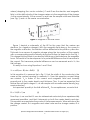
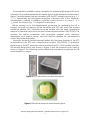
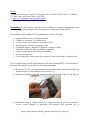
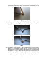
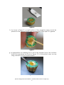
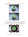
Hall Effect Measurement in Copper
(Electrical Transport Option)
Prof. Richard Averitt, UC San Diego
Description: The objective of this educational module (EM) is to measure the Hall
voltage VH to determine the Hall coefficient RH of Cu, a monovalent metal. VH in
metals is typically quite small (~microvolts for reasonable values of the applied
current and magnetic field), but is easily measured using VersaLab/ETO. This EM
will familiarize students with basic properties of simple metals and technical
aspects of using the VersaLab/ETO to make small signal transport measurements.
In addition, students will learn basic aspects of sample handling, soldering, and
data acquisition and analysis.
Hall Effect: The Hall effect (HE)1, arises from the sideways deflection of charges in
a conductor upon application of a magnetic field. This effect was discovered in
1879 by Edwin Hall and, as described below, provides a method to determine the
concentration (n) and sign (e.g. electrons or holes) of the charge carriers. The HE
is now used extensively in characterizing metals, semiconductors, and
ferromagnets2. In two-dimensional conductors the integer quantum Hall effect
(IQHE) and fractional-QHE (FQHE) have been discovered leading to Nobel prizes
in 1985 and 1998. Recently, the QHE has been observed in graphene at room
temperature3. Finally, we mention that VH is sufficiently large in semiconductors
enabling the development of Hall probes, which are used as compact
inexpensive magnetometers.
For a simple understanding of the HE, it is sufficient to consider the Lorentz force,
𝑭𝑭 = 𝑒𝑒𝑬𝑬 + 𝑒𝑒(𝒗𝒗𝑑𝑑 × 𝑩𝑩) (1)
and the current density,
𝑰𝑰
𝑱𝑱 = 𝑤𝑤𝑤𝑤 = 𝑛𝑛𝑛𝑛𝒗𝒗𝑑𝑑
(2)
Quantum Design Educational Module – Hall Effect Measurement in Copper (v.1)
1
where (dropping the vector notation), E and B are the electric and magnetic
field, vd is the drift velocity of the charge carriers, e is the magnitude of the charge,
J is the current density, I is the current, w and t are the sample width and thickness
(see. Fig. 1) and n is the carrier concentration.
Figure 1: diagram of the Hall Effect
Figure 1 depicts a schematic of the HE for the case that the carriers are
electrons (i.e. negative charges). With the magnetic field along z, the current in
the negative x direction, the electron will be deflected in the positive y direction.
This leads to an excess of negative charge along the top portion of the sample,
with a corresponding positive density along the bottom as depicted in the Fig. 1.
This charge build up leads to an electric field along y that balances the magnetic
force. This results in the development of a potential difference that is transverse to
the current. This transverse potential difference can be measured and is VH, the
Hall voltage.
It is easy to show using Equations 1 and 2 that,
VH = wJB/ne = IB/nte = RHIB/t
(3)
In this equation it is assumed (as in Fig. 1) that the width of the conductor is the
same as the contact spacing to measure VH. From this equation, several things
are evident. VH is linear in the current and magnetic field and inversely
proportional to the carrier density and thickness. Thus, it can be expected that
thinner films will yield a larger VH, as will samples with a smaller carrier density (e.g.
semiconductors).
An important quantity is the Hall efficient RH. For completeness, we note that
RH = VHt/IB = 1/ne
(4)
From Eqn. 4, we see that RH can be determined exclusively from experimentally
measured quantities, and that it depends on both the carrier density and sign.
This equation encapsulates the power of Hall measurements. When electrons are
the charge carriers, RH is negative and when holes are the charge carriers, RH is
positive.
Quantum Design Educational Module – Hall Effect Measurement in Copper (v.1)
2
It is important to establish a clear convention in determining the sign of RH since,
otherwise, it is possible misidentify the carrier type in a Hall transport measurement.
Figure 1 includes labels that are consistent with the ETO transport pucks (e.g. I+, I-,
V+, V-). Specifically, the field points along the z-direction that, in the VersaLab,
corresponds to vertical. In addition, a positive current is from I+ to I- and V+ - V- =
VH which, as shown in Fig. 1, is negative for electrons.
Before moving on to the experimental procedure for measuring the HE in
copper, we point out aspects of the VersaLab and ETO with which the student
should be familiar. First, students should be familiar with the basic operational
aspects of VersaLab as found in the user’s manual (part number 1300-001,B0). This
includes the helium compressor and cryocooler, magnet, puck interface,
diaphragm and sorption pump, and the MultiVu software for measurement
control and data acquisition.
Secondly, students should become familiar with the basic features of the ETO
as described in the ETO user’s manual (part number 1084-700,B0). Of particular
importance is the ETO hardware which includes the ETO CM-H module and EMQN remote head which are shown in Figure 2 and the transport puck which is
shown in Figure3. The following section details the procedures to perform the HE
measurement in copper.
Figure 2: ETO electronics: module and head
Figure 3: Electrical transport measurement puck
Quantum Design Educational Module – Hall Effect Measurement in Copper (v.1)
3
Notes:
1. See, for example, Chapter 6 of Introduction to Solid State Physics, 7th edition,
C. Kittel, Wiley and Sons, New York 1996.
2. http://en.wikipedia.org/wiki/Hall_effect
3. Y. Zhang, et al, Nature 438, 201 (2005).
Instructions: In this section, we will provide details on sample preparation and,
subsequently, performing the HE measurement using the VersaLab/ETO.
Several items are needed for this experiment, which includes:
•
•
•
•
•
•
•
•
•
Copper foil less than 100 microns thick
Caliper to measure Cu foil thickness
Cotton swabs and acetone to clear Cu foil
Soldering iron, solder, thin gauge wire
Cigarette paper + Apiezon H grease, or Kapton tape
Tweezers, toothpick (for spreading H grease)
Latex or nitrile gloves for sample handling
ETO transport puck
Puck wiring test station and ohm meter (to test continuity of solder joints)
Prior to performing the HE measurement with the VersaLab/ETO, it is important to
prepare the sample as detailed in the following steps:
a.) From the Cu foil, cut a square piece and make sure it can lie flat within the
square region of the sample puck (see Fig. 3).
b.) Using the calipers, measure and record the thickness of the Cu foil (Fig. 4).
Figure 4
c.) As shown in Fig. 5, clean the Cu foil using tweezers to hold the sample. A
cotton swab dipped in acetone will remove any residual oils or
Quantum Design Educational Module – Hall Effect Measurement in Copper (v.1)
4
contaminants, facilitating soldering and minimizing contamination of the
VersaLab sample chamber.
Figure 5
d.) As shown in Fig. 6 and 7, solder a short section of wire onto each corner of
the Cu foil. The excess length of wire can be cut off upon soldering the
sample to the transport puck (step h, below).
Figure 6
Figure 7
e.) The transport puck is metallic in order to maintain good thermal contact
between the sample and cold head. However, to prevent shorting of the
sample, electrical isolation is need. This can be achieved, for example, with
Kapton tape. In Figure 8, we show an alternative option where we will use
cigarette paper and Apiezon H grease. Apiezon H is a silicone-free high
thermal conductivity grease suitable for high vacuum applications.
Quantum Design Educational Module – Hall Effect Measurement in Copper (v.1)
5
Figure 8
f.) As shown in Figure 9, a small section of the cigarette paper should be
placed on the transport puck and covered with a thin layer of H grease.
Figure 9
g.) In preparation for soldering the Cu foil to the transport puck, the contacts
should be pre-tinned as shown in Figure 10. In the present case, we are
using channel 2 for the measurements.
Figure 10
Quantum Design Educational Module – Hall Effect Measurement in Copper (v.1)
6
h.) As shown in Figure 11 and 12, the Cu foil should be placed on the transport
puck, soldering each wire and then cutting off the excess.
Figure 11
Figure 12
i.) Figure 13 shows the transport puck /Cu foil attached to the puck wiring test
station. Importantly, notice the how the wires are soldered with V+ and Valong one diagonal and I+ and I- along the other diagonal, in a
configuration that is consistent with the convention for the HE described in
Figure 1.
Figure 13
Quantum Design Educational Module – Hall Effect Measurement in Copper (v.1)
7
j.) As shown in Figure 14, the puck wiring test station provides a convenient
means to check the continuity of the soldering prior to insertion into the
VersaLab instrument. If the solder joints are good, a resistance of less then
one ohm will be measured across any of the contacts.
Figure 14
k.) At this point the transport puck/Cu foil is ready to be inserted into the
VersaLab. This is accomplished using the puck insertion tool as described in
the VersaLab user’s manual (Figure 1-2). Upon inserting the puck, it is
important to make sure the tab on the transport puck is properly aligned.
The tab should face towards the front of the VersaLab, and it is possible to
feel a slight click. At this point gentle downward pressure will allow for
appropriate seating of the sample puck into the sample chamber.
l.) The sample chamber can be sealed by inserting the baffle set (don’t forget
the o-ring) and Kwik-Flange clamp.
The rest of this experiment will utilize the MultiVu software. Please see Chapter 3 of
the VersaLab manual and Chapter 4 of the ETO manual for complete details.
m.) Activate the ETO option. Under the utilities tab, select activate option.
Under the "Available Options" select "Electrical Transport" and then click
the activate button. This will activate the instrument and pull up the ETO
console.
n.) On the ETO console, click the "Datafile" tab and choose a sample name
and location for your data to be saved. There are default settings. Click
"Change" to alter the name and location of the datafile.
o.) While not required for this measurement, it is useful to know how to pump
down the sample chamber. Under the "Instrument" tab, select "Chamber".
This will pull up a dialog box. Under "Control" select "Purge/Seal" to initiate
putting the sample under vacuum. The left hand side of the dialog box will
show the status. This will reduce the sample vacuum to a few torr. To obtain
high vacuum, click the "HiVac" tab.
Quantum Design Educational Module – Hall Effect Measurement in Copper (v.1)
8
p.) The next step is to write a sequence to perform the required measurement.
Under the "file" tab, click new sequence. This will open a new sequence file
(e.g. Sequence1.seq) and the sequence command bar. Double click
"Scan Field" to open another dialog box to enter the desired parameters.
For example, you might choose an initial field of 10000 Oe and a final field
of -10000 Oe in steps of 1000 Oe. The maximum rate that can be chosen is
300 Oe/sec. Once your selections are made, click "ok" to insert the
command line into the sequence file.
q.) Returning to the sequence command bar, click "Electrical Transport" and
then double click “ETO Resistance”. This will pull up the "AC Resistance
Measurement" box. Since we have wired up the sample on channel two,
select "Enable Measurement" for Channel 2. For the excitation, choose
100mA and 21.3 Hz. Select autorange, and for the measurement
configuration choose a one second averaging time and 5 for the number
of measurements. Upon clicking “ok”, these selections will be inserted into
the sequence.
r.) This constitutes a complete, albeit short, measurement sequence to
measure the HE on copper. The sequence can be saved by selecting the
"file" tab and "save as" to select a file name and location.
s.) To initiate the measurement sequence, click the "play" button near the top
of the MultiVu software interface. This will start the data acquisition with the
data being save under the filename you selected in step o.) above.
t.) At the bottom of the MultiVu software, the status of the temperature, field,
and vacuum can be monitored.
u.) To monitor the data collection in real time click the "Datafile" tab on the
ETO console and select "View". This will plot the data in real time. The default
is to show the time stamp on the x-axis, and to plot the resistance and
phase angle of both channels one and two. To change this right click on
the plot and choose "data selection" to bring up a dialog box to change
the view. Change the x-axis to plot field and deselect the boxes for channel
one and the phase angle of channel 2. The result is that the Hall resistance
will be plotted as a function of the field. Right click on the plot and choose
"autoscale" to see the complete data set.
v.) At the end of the measurement sequence, you should obtain a plot of the
Hall resistance as a function of field as shown in Fig. 15.
Quantum Design Educational Module – Hall Effect Measurement in Copper (v.1)
9
Figure 15
w.) To return to the zero field condition select the "Instrument" tab and choose
"field." This will open a dialog box. Enter a setpoint of 0 Oe and click "set".
This will ramp the field down to zero. After venting the sample (if under
vacuum), the sample can be removed.
x.) Looking at this data, it is clear that the negative slope is consistent with
electrons as the change carriers in copper. Using this data, it is possible to
calculate the Hall coefficient and determine the carrier density. As a final
note, the data clearly shows that the data does not go through zero at zero
field. This arises from the imperfect alignment of the Hall voltage contacts.
A very slight misalignment from 90 degrees with respect to the direction of
the current, results in a longitudinal component being present in the
transverse data. In the present case, this can be subtracted from the data
prior to a more complete analysis.
Questions / Analysis: Some of the following questions are specific to the data that
was obtained, while others are of a more open-ended or comparative nature.
Quantum Design Educational Module – Hall Effect Measurement in Copper (v.1)
10
1. From your data, determine the Hall coefficient for RH copper. Determine
the carrier density of your sample. Make certain to include the error bars for
your data, along with a brief description of your error analysis.
2. Compare your results to existing values in the in the literature (be certain to
cite your sources). Discuss possible discrepancies in terms of samples,
sources of error, assumptions in your analysis, and anything else you
consider as a potential contributing factor.
3. Find the value of RH for single crystal Cu & discuss the difference with your
measurements on polycrystalline samples.
4. What would you expect to happen to RH with decreasing temperature?
Why? If you would like (or have not already done so), measure RH at 50K to
see if your experimental results agree with your expectations.
5. Obtain a piece of Zn and measure the Hall effect. Repeat your
determination of RH and the carrier density, and discuss the differences
between Cu and Zn.
Quantum Design Educational Module – Hall Effect Measurement in Copper (v.1)
11