1
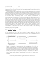
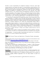
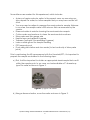
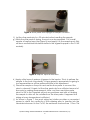
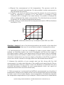
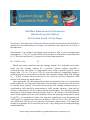
Hall Effect Measurement in Germanium
(Electrical Transport Option)
Prof. Richard Averitt, UC San Diego
Description: The objective of this educational module is to measure the Hall effect
germanium and determine the carrier concentration (and type) as a function of
temperature.
Germanium is an indirect bandgap semiconductor with a room temperature
bandgap EG = 0.67 eV. As discussed in the module on Hall effect measurements
in Cu, the Hall coefficient RH is given by the following equation:
RH = VHt/IB = 1/ne
(1)
Recall that when electrons are the charge carriers, RH is negative and when
holes are the charge carriers, RH is positive. Typical carriers densities in
semiconductors are orders of magnitude lower than in metals (typical values
range from ~1014 to 1018 cm-3). Thus, RH can be orders of magnitude larger in
semiconductors in comparison to metals. The correspondingly large Hall voltage
(VH = RHIB/t) enables semiconductors to be used as low-cost magnetic field
sensors with numerous applications1.
More generally, HE measurements provide a powerful means to characterize
semiconductors, an important task given the ubiquity of semiconductor devices
in virtually every aspect of modern technology. Hall voltage measurements, in
combination with resistivity measurements (with certain caveats – see below),
suffice to determine both the carrier density and mobility. The mobility (typically
denoted µ) characterizes the drift velocity, that is v = µE where v is the drift velocity
and E is the applied electric field. Mobility values are typically presented in terms
of cm2/Vs – for example in GaAs, the electron mobility at room temperature is
~8500 cm2/Vs, whereas for holes the mobility is ~400 cm2/Vs. In Ge, the numbers
are ~3900 and 1900 cm2/Vs for electrons and holes, respectively2. The larger the
mobility the greater the conductivity since σ = neµ, along with a correspondingly
smaller resistivity:
Quantum Design Educational Module – Hall Effect Measurement in Germanium (v.1)
1
ρ = 1/σ = 1/ neµ
(2)
A glance at Eqns. (1) and (2) shows that these determining RH and ρ allows for the
determination of n and µ.
These equations are a simplification, and would be appropriate for a material
where either electrons or holes are the dominant carriers. In semiconductors, both
electrons and holes can simultaneously contribute to the transport, and they must
be treated, initially at least, on equal footing. A basic understanding of this can
be obtained from considering Figure 1. The defining characteristic of
semiconductors is the existence of a nonzero bandgap with typical values on the
order of 1 eV. For an intrinsic semiconductor as depicted in Fig. 1(a) (i.e. one
without intentional doping), this leads to a small carrier density that is determined
via thermal activation across the gap. Intuitively, the larger the gap, the smaller
the carrier density at a given temperature. For intrinsic semiconductors, for each
electron thermally excited across the gap into the conduction band, there is a
corresponding hole in the valence band, both of which contribute to the
transport properties of the material – this is often termed ambipolar transport.
Consideration of electrons and holes to the transport leads to the following
expression for the Hall voltage:
𝑉𝑉𝐻𝐻 =
2
𝑝𝑝𝑝𝑝ℎ
−𝑛𝑛𝑛𝑛𝑒𝑒2
𝑒𝑒(𝑝𝑝𝑝𝑝ℎ −𝑛𝑛𝑛𝑛𝑒𝑒 )2
𝑝𝑝−𝑛𝑛𝑛𝑛2
= 𝑒𝑒(𝑝𝑝+𝑛𝑛𝑛𝑛)2
(3)
In this equation, p (n) is the hole (electron) carrier density, µp (µe) the
corresponding hole (electron) mobility, and θ = µe/µh. Eqn. (3) highlights that the
Figure 1: schematic of semiconductor with energy gap EG. a) For an
intrinsic semiconductor (i.e. undoped), the Fermi energy EF (more properly,
the chemical potential) is at ½EG. b) The addition of donors with binding
energy ED increases the conduction band carrier density (electrons) while
doping with acceptors with binding energy EA, increases the valence
band carrier density (holes). Doping leads to a shift of EF away from
midgap.
Quantum Design Educational Module – Hall Effect Measurement in Germanium (v.1)
2
situation is more complicated for ambipolar transport3. However, quite often
semiconductors are doped with atoms to create extrinsic semiconductors. The
addition of donors (e.g. P or As in Ge, see Fig. 1 (b)) adds additional electrons to
the conduction band at temperatures sufficient to ionize the donor impurities.
Similarly, the addition of acceptors (e.g. B or Al in Ge, see Fig. 1(c)), adds
additional holes to the valence band at temperatures sufficient to ionize the
acceptor impurities. If the dopant density is sufficiently larger that the intrinsic
carrier density then Eqn. 3 simplifies. For example, if the acceptor dopant density
is such that 𝑝𝑝 >> 𝑛𝑛𝜃𝜃 2 , then Eqn. 3 simplifies to the conventional form (i.e. Eqn. 1,
note however, we now have separate symbols – 𝑝𝑝 for holes and 𝑛𝑛 for electrons).
It is important to emphasize that temperature plays a key role because of the
thermal excitation of carriers across the gap and because of donor thermal
ionization. A given doped semiconductor could exhibit extrinsic behavior at room
temperature with a crossover to intrinsic behavior with decreasing temperature
because of dopant freeze-out (i.e. below the temperature where there is
appreciable dopant ionization). A crossover to intrinsic behavior could also occur
at higher temperatures because of thermal excitation of carriers across the gap
in excess of the dopant density. Temperature dependent HE measurements
enable the determination of this behavior. Excellent discussions of the statistical
mechanics of carrier density in intrinsic and extrinsic semiconductors can be
found in the notes4.
Versalab can be used to measure the Hall effect and the resistivity. However,
in this module, we will focus on Hall measurements of p-doped Ge as a function
of temperature. It may be useful to go back and review the Cu Hall Effect
module as it contains complementary information.
Notes:
1. Hall-Effect Sensors: Theory and Application, E. Ramsden, Elsevier, Amsterdam
2006.
2. An excellent online source for the properties of numerous semiconductors can
be found at http://www.ioffe.ru/SVA/NSM/Semicond/
3. It is worth mentioning at this point that a more complete analysis of the Hall
Effect must treat the statistical nature of the carrier velocity, leading to prefactor
in Eqn. 1 or 3 that is ~1.
4. Chapter 8 of Introduction to Solid State Physics, 7th edition, C. Kittel, Wiley and
Sons, New York 1996; Chapter 28 of Solid State Physics, N. W. Ashcroft and N.D.
Mermin, W.B. Saunders, Philadelphia 1976; Chapter 1of Physics of
Semiconductor Devices, S.M. Sze, Wiley & Sons, New York 1981.
Instructions: In this section, we will provide details on sample preparation and,
subsequently, performing the HE measurement using the VersaLab/ETO. We note
that the approach is similar to the Cu Hall effect measurements, but we there we
will take a slightly different approach if for no other reason to point out
alternatives.
Quantum Design Educational Module – Hall Effect Measurement in Germanium (v.1)
3
Several items are needed for this experiment, which includes:
•
•
•
•
•
•
•
•
•
•
A piece of semiconductor wafer. In the present case, we are using a ptype doped Ge wafer, but other samples that you may have access will
work.
You may need a caliper to measure the semiconductor sample thickness.
In our case, the sample wafer is 500 microns thick as measured by the
vendor.
Diamond scribe to assist in cleaving the semiconductor sample
Cotton swabs and acetone to clean the semiconductor surface
Silver paste and thin gauge wire
Kapton tape and apiezon N grease
Tweezers, toothpick (for spreading H grease)
Latex or nitrile gloves for sample handling
ETO transport puck
Puck wiring test station and ohm meter (to test continuity of silver paste
joints)
Prior to performing the HE measurement with the VersaLab/ETO, it is important to
prepare the sample as detailed in the following steps:
a.) First, it will be important to obtain an appropriate sized sample that can fit
within the sample puck. In our case, we had available a 2” diameter ptype Ge wafer as shown in Figure 2.
Figure 2: p-type Ge wafer
b.) Using a diamond scribe, score the wafer as shown in Figure 3.
Quantum Design Educational Module – Hall Effect Measurement in Germanium (v.1)
4
Figure 3: Score the wafer with a diamond scribe
c.) Place the wafer with the scribed line along a straight edge such as a
microscope slide and press gently. The wafer should break along the
scribed line as shown in Figure 4. Repeat this process along the orthogonal
directions until you have a square sample. Other approaches may be
more precise depending on the equipment available in your lab (e.g.
wafer saw).
Figure 4: Cleaved Ge wafer
d.) The sample should be cleaned with acetone prior to mounting on the
wafer puck and wiring up.
e.) For this sample we, instead of soldering we will attach the leads using
silver paste (Fig. 5). A sharp tip such as a syringe will be useful to precisely
locate the soldering paste and wires. For good adhesion to the wafer, we
first used the diamond scribe to gently scratch the area where the silver
paste will be applied. The process is quite similar to soldering as described
in the Cu Hall Effect module.
Quantum Design Educational Module – Hall Effect Measurement in Germanium (v.1)
5
Figure 5: Silver paste and syringe for sample contacts
f.) Let the silver paste dry for ~20 minutes before handling the sample.
g.) While the silver paste is drying, the puck can be prepared. Cut a small
sample of kapton tape (see Figure 6) and apply it to the sample puck (this
will serve as elelctrical insulation similar to the cigarette paper in the Cu HE
module).
Figure 6: Kapton tape as insulation
h.) Apply a thin layer of apiezon N grease to the kapton. This is to adhere the
sample to the puck. Importantly, N-type grease is appropriate for going to
low temperatures as will be performed later in this experiment.
i.) Place the sample on the puck and use the silver paste to connect the
wires to channel 2. Again, let the sliver paste dry for a sufficient amount of
time prior to making measurements. Note: we have used silver paste
down to 50K in the VersaLab without any problems and with out baking
the sample to drive off the volatiles from the silver paste. It appears that
drying at room temperature is sufficient.
j.) As shown in Figure 7, the puck wiring test station provides a convenient
means to check the continuity of the soldering prior to insertion into the
VersaLab instrument. In the Cu HE, the resistance was less than 1 Ohm. This
Quantum Design Educational Module – Hall Effect Measurement in Germanium (v.1)
6
need not be the case for the semiconductor and as Fig. 6 shows, for our
sample the resistance is ~0.9 kΩ.
Figure 7: Checking sample for continuity
k.) At this point the transport puck/Cu foil is ready to be inserted into the
VersaLab. This is accomplished using the puck insertion tool as described in
the VersaLab user’s manual (Figure 1-2). Upon inserting the puck, it is
important to make sure the tab on the transport puck is properly aligned.
The tab should face towards the front of the VersaLab, and it is possible to
feel a slight click. At this point gentle downward pressure will allow for
appropriate seating of the sample puck into the sample chamber.
l.) The sample chamber can be sealed by inserting the baffle set (don’t forget
the o-ring) and Kwik-Flange clamp.
The rest of this experiment will utilize the MultiVu software. Please see Chapter 3 of
the VersaLab manual and Chapter 4 of the ETO manual for complete details.
Moreover, the sequence is similar to the Cu Hall Effect, so please refer to steps m.)
– v.) of the Cu HE module.
m.) One difference is that for the Cu HE, we used a current of 100mA. That is
more than required for these measurements. Try using 1mA to determine if
that is sufficient to obtain a good signal. That is what we used for the
measurements of our p-type Ge Sample.
n.) The measurement you performed was at room temperature. As per the
discussion above, we expect the carrier concentration to change as a
function of temperature. We will manually cool the sample to 150K (i.e. not
using a sequence). To do this, right click in the temperature box in the lower
left corner of MultiVu. This will pull up the dialog box. Enter 150K, with a
cooling rate of 10K/min and push set. Wait for the temperature to stabilize.
Quantum Design Educational Module – Hall Effect Measurement in Germanium (v.1)
7
o.) Repeat the measurement at this temperature. This process could be
repeated at several temperatures. It is also possible to write a sequence to
fully automate this process.
p.) In Figure 7, we show our data for the p-type Ge sample. As can be seen the
slope, as expected is opposite to Cu, and there is a change in slope
consistent with a change in the carrier density. It is possible to analyze this
data to determine the carrier concentration. This data has been processed
to subtract off the residual longitudinal resistance.
q.) Finally, when you are finished set the temperature back to 300K and reduce
the field to 0 Oe.
Figure 8: Hall measurements in p-Ge sample: black 300K, red 150K
Questions / Analysis: Some of the following questions are specific to the data that
was obtained, while others are of a more open-ended or comparative nature.
1. In semiconductors, it can be a challenge to make a good ohmic contact.
Instead, as Schottkey barrier can result. Investigate and discuss the origin of
Schottkey barriers. Identify some approaches that have been used to eliminate
Schottkey barriers and achieve a good ohmic contact. How would you use the
VersaLab to determine if you have an ohmic or Schottky contact? Do you expect
have a non-ohmic contact to strongly affect the Hall measurement results?
2. Measure the resistivity of your sample and use this, along with the Hall
measurement, to obtain and estimate of the mobility and carrier density. Discuss
any approximations that you make. Look in the literature to determine the most
accurate techniques available for such measurements (note: you need not
implement these more accurate techniques).
3. Write a sequence to automate the Hall Effect measurements as a function of
temperature. Measure your sample at ten or more temperatures and use this data
to make a plot of the carrier density versus temperature. Qualitatively describe
the temperature dependence of your sample. Is there evidence for carrier freeze
Quantum Design Educational Module – Hall Effect Measurement in Germanium (v.1)
8
out (i.e. do you go to temperatures sufficiently low that you don’t ionize the
impurities?) Some of these questions can be very sample dependent so you may
need to think carefully about your results with regards to the room temperature
dopant density, etc.
4. What does the change in slope between the 300K data and 150K data in Figure
7 suggest? That is, is this data in line with your intuitive expectations for what should
occur upon cooling?
5. Either derive or find a derivation of Equation 3 for the Hall voltage when electron
and holes both contribute to the transport.
Quantum Design Educational Module – Hall Effect Measurement in Germanium (v.1)
9