1
Electron Transport in GaAs Heterostructures
at Various Magnetic Field Strengths
a dissertation presented by
Jeffrey Burnham Miller
to the Division of Engineering and Applied Science
in partial fulfillment of the requirements for the degree of
Doctor of Philosophy
in the subject of
Applied Physics
Harvard University
Cambridge, Massachusetts
January, 2007
©2007 Jeffrey Burnham Miller
All rights reserved.
Dissertation Advisor: Professor Charles M. Marcus
Author: Jeffrey B. Miller
Electron Transport in GaAs Heterostructures
at Various Magnetic Field Strengths
Abstract
This thesis describes two sets of experiments which explore transport in a two-dimensional electron gas in the presence of a magnetic field. We used nanofabrication techniques to make samples
on GaAs/AlGaAs heterostructures, and measured the samples at cryogenic temperatures using
ac-lock-in techniques.
In the first set of experiments—the low-field experiments—we studied the effect of spinorbit coupling. We tuned the strength of spin-orbit coupling from the weak localization regime to
the antilocalization regime using in situ gate control. Using a new theory, we separately extracted
the values for the three material-dependent spin-orbit constants. We also measured the average
and variance of conductance in assorted quantum dots, with and without strong spin-orbit coupling, and found quantitative agreement with recent random matrix theory predictions, as long
as we also properly included the effects of parallel magnetic field.
In the second set of experiments—the high-field experiments—we studied the transport
properties of quantum point contacts (qpc) fabricated on a GaAs/AlGaAs two dimensional electron gas that exhibits excellent bulk fractional quantum Hall effect, including a strong plateau in
the Hall resistance at Landau level filling fraction ν = 5/2. We demonstrate that the ν = 5/2 state
can survive in qpcs with 1.2 µm and 0.8 µm spacings between the gates. However, in our sample,
all signatures of the 5/2 state are completely gone in a 0.5 µm qpc. We study the temperature dependence at ν = 5/2 in the qpc and find two distinct regimes: at temperatures below 19 mK a we
find a plateau-like feature with resistance near (but above) the bulk quantized value of 0.4 h/e2 ,
while at higher temperatures this plateau does not form. We study the dc-current-bias (Idc ) dependence of the plateau-like feature, and find a peak in the differential resistance at Idc = 0 and
a dip around Idc ∼ 1.2 nA, consistent with quasiparticle tunneling between fractional edge states.
In a qpc with 0.5 µm spacing between the gates, we do not observe a plateau-like feature at any
temperature, and the Idc characteristic is flat for the entire range between ν = 3 and ν = 2.
iii
iv
Contents
Abstract
iii
Acknowledgements
ix
1 Introduction
1
2 Introduction to the 5/2 experiment
2.1 Overview . . . . . . . . . . . . . . . . . . . . . . . . .
2.2 Theoretical Background . . . . . . . . . . . . . . . .
2.2.1 General introduction to quantum computers
2.2.2 Introduction to anyons . . . . . . . . . . . . .
2.2.3 Integer and fractional quantum Hall effects
2.2.4 Topological Quantum Computation . . . . .
2.3 Prior experimental work . . . . . . . . . . . . . . . .
2.4 Impact of this work and future directions . . . . . .
2.5 Techniques . . . . . . . . . . . . . . . . . . . . . . . .
2.5.1 Refrigerator and wiring . . . . . . . . . . . .
2.5.2 LED . . . . . . . . . . . . . . . . . . . . . . . .
2.5.3 Electron Temperature . . . . . . . . . . . . .
.
.
.
.
.
.
.
.
.
.
.
.
3 Introduction to the spin-orbit coupling experiments
3.1 Theoretical background . . . . . . . . . . . . . . . . .
3.1.1 Spin-orbit coupling . . . . . . . . . . . . . . . .
3.1.2 Weak localization and antilocalization . . . . .
3.1.3 Conductance fluctuations . . . . . . . . . . . .
3.1.4 Physics in the dot and random matrix theory
3.2 Perspectives on the 2d spin-orbit experiment . . . . .
3.3 Perspectives on the quantum-dot experiments . . . .
3.4 Techniques . . . . . . . . . . . . . . . . . . . . . . . . .
3.4.1 Data Acquisition . . . . . . . . . . . . . . . . .
3.4.2 Data Analysis . . . . . . . . . . . . . . . . . . .
.
.
.
.
.
.
.
.
.
.
.
.
.
.
.
.
.
.
.
.
.
.
.
.
.
.
.
.
.
.
.
.
.
.
.
.
.
.
.
.
.
.
.
.
.
.
.
.
.
.
.
.
.
.
.
.
.
.
.
.
.
.
.
.
.
.
.
.
.
.
.
.
.
.
.
.
.
.
.
.
.
.
.
.
.
.
.
.
.
.
.
.
.
.
.
.
.
.
.
.
.
.
.
.
.
.
.
.
.
.
.
.
.
.
.
.
.
.
.
.
.
.
.
.
.
.
.
.
.
.
.
.
.
.
.
.
.
.
.
.
.
.
.
.
.
.
.
.
.
.
.
.
.
.
.
.
.
.
.
.
.
.
.
.
.
.
.
.
.
.
.
.
.
.
.
.
.
.
.
.
.
.
.
.
.
.
.
.
.
.
.
.
.
.
.
.
.
.
.
.
.
.
.
.
.
.
.
.
.
.
.
.
.
.
.
.
.
.
.
.
.
.
.
.
.
.
.
.
.
.
.
.
.
.
.
.
.
.
.
.
.
.
.
.
.
.
.
.
.
.
.
.
.
.
.
.
.
.
.
.
.
.
.
.
.
.
.
.
.
.
.
.
.
.
.
.
.
.
.
.
.
.
.
.
.
.
.
.
.
.
.
.
.
.
.
.
.
.
.
.
.
.
.
.
.
.
.
.
.
.
.
.
.
.
.
.
.
.
.
.
.
.
.
.
.
.
.
.
.
.
.
.
.
.
.
.
.
.
.
.
.
.
.
.
.
.
.
.
.
.
.
.
.
.
.
.
.
.
.
.
.
.
.
.
.
.
.
.
.
.
.
.
.
.
.
.
.
.
.
.
.
.
.
.
.
.
3
3
4
4
5
7
11
13
15
17
17
17
18
.
.
.
.
.
.
.
.
.
.
21
21
21
22
23
23
24
25
27
27
27
4 Spin-Orbit in Two Dimensions
4.1 Introduction . . . . . . . . . . . . . . . . . . . . . . . . . . . . . . . . . . . . . . . . . .
4.2 Previous Theory and Experiments . . . . . . . . . . . . . . . . . . . . . . . . . . . . .
4.3 Theory of Two-Dimensional Magnetotransport with Spin-Orbit Coupling beyond
the Diffusive Approximation . . . . . . . . . . . . . . . . . . . . . . . . . . . . . . . .
4.4 Experimental Details . . . . . . . . . . . . . . . . . . . . . . . . . . . . . . . . . . . . .
4.5 Crossover from WL to AL and Separation of Spin-Orbit Parameters . . . . . . . . .
4.6 Angular Dependence of Spin Precession Rates . . . . . . . . . . . . . . . . . . . . . .
4.7 Comparison with previous Theory . . . . . . . . . . . . . . . . . . . . . . . . . . . . .
4.8 Conclusion . . . . . . . . . . . . . . . . . . . . . . . . . . . . . . . . . . . . . . . . . . .
4.9 Acknowledgements . . . . . . . . . . . . . . . . . . . . . . . . . . . . . . . . . . . . . .
v
29
30
30
31
32
33
34
34
35
36
5 Antilocalization in Quantum Dots
5.1 Introduction . . . . . . . . . . . . . . . . . . . . . . . . . . . . . . . . . . .
5.2 Previous Experiments . . . . . . . . . . . . . . . . . . . . . . . . . . . . .
5.3 Random Matrix Theory . . . . . . . . . . . . . . . . . . . . . . . . . . . .
5.4 Antilocalization and Confinement Suppression of Spin-Orbit Effects . .
5.5 Suppression of Antilocalization by an In-Plane Magnetic Field . . . . . .
5.6 Breaking of Time-Reversal Symmetry due to an In-Plane Magnetic Field
5.7 Effects of Temperature on Antilocalization . . . . . . . . . . . . . . . . .
5.8 In Situ Control of Spin-Orbit Coupling with a Center Gate . . . . . . . .
5.9 Acknowledgements . . . . . . . . . . . . . . . . . . . . . . . . . . . . . . .
.
.
.
.
.
.
.
.
.
.
.
.
.
.
.
.
.
.
.
.
.
.
.
.
.
.
.
.
.
.
.
.
.
.
.
.
.
.
.
.
.
.
.
.
.
.
.
.
.
.
.
.
.
.
.
.
.
.
.
.
.
.
.
37
38
38
38
39
40
42
42
42
44
6 Conductance Fluctuations in Quantum Dots
6.1 Introduction . . . . . . . . . . . . . . . . . . . . . . . . . . . . .
6.2 Previous Work . . . . . . . . . . . . . . . . . . . . . . . . . . . .
6.3 Spin-Rotation Symmetry Classes . . . . . . . . . . . . . . . . .
6.4 Experimental Techniques . . . . . . . . . . . . . . . . . . . . .
6.5 Characterization of Spin-Orbit Strength at Zero In-Plane Field
6.6 Variance at Zero In-Plane Field . . . . . . . . . . . . . . . . . .
6.7 Effects of Spin-Rotation Symmetry on the Variance . . . . . .
6.8 Orbital effects of Bk on the Variance . . . . . . . . . . . . . . .
6.9 Conclusion . . . . . . . . . . . . . . . . . . . . . . . . . . . . . .
6.10 Acknowledgements . . . . . . . . . . . . . . . . . . . . . . . . .
.
.
.
.
.
.
.
.
.
.
.
.
.
.
.
.
.
.
.
.
.
.
.
.
.
.
.
.
.
.
.
.
.
.
.
.
.
.
.
.
.
.
.
.
.
.
.
.
.
.
.
.
.
.
.
.
.
.
.
.
.
.
.
.
.
.
.
.
.
.
.
.
.
.
.
.
.
.
.
.
.
.
.
.
.
.
.
.
.
.
45
46
46
46
47
47
48
49
50
51
52
7 Experimental observation of the ν = 5/2 state in a quantum point contact
7.1 Introduction . . . . . . . . . . . . . . . . . . . . . . . . . . . . . . . . . .
7.2 Measurement Techniques . . . . . . . . . . . . . . . . . . . . . . . . . .
7.3 Previous Experiments . . . . . . . . . . . . . . . . . . . . . . . . . . . .
7.4 Experimental Details . . . . . . . . . . . . . . . . . . . . . . . . . . . . .
7.5 Bulk Measurements . . . . . . . . . . . . . . . . . . . . . . . . . . . . . .
7.6 Demonstration of the qpc in iqhe and fqhe regimes . . . . . . . . . .
7.7 Observation of plateaus at ν = 5/2 . . . . . . . . . . . . . . . . . . . . .
7.8 Temperature data in the qpc . . . . . . . . . . . . . . . . . . . . . . . . .
7.9 Idc data . . . . . . . . . . . . . . . . . . . . . . . . . . . . . . . . . . . . .
7.10 Conclusion . . . . . . . . . . . . . . . . . . . . . . . . . . . . . . . . . . .
7.11 Acknowledgements . . . . . . . . . . . . . . . . . . . . . . . . . . . . . .
.
.
.
.
.
.
.
.
.
.
.
.
.
.
.
.
.
.
.
.
.
.
.
.
.
.
.
.
.
.
.
.
.
.
.
.
.
.
.
.
.
.
.
.
.
.
.
.
.
.
.
.
.
.
.
.
.
.
.
.
.
.
.
.
.
.
.
.
.
.
.
.
.
.
.
.
.
.
.
.
.
.
.
.
.
.
.
.
53
54
55
55
55
56
57
58
58
59
61
61
.
.
.
.
.
.
.
.
.
.
.
.
.
.
.
.
.
.
.
.
.
.
.
.
.
.
.
.
.
.
.
.
.
.
.
.
.
.
.
.
63
A Raith Users Guide
.
.
.
.
.
.
.
.
.
.
.
.
.
.
.
.
.
.
.
.
.
.
.
.
.
.
.
.
.
.
.
.
.
.
.
.
.
.
.
.
.
.
.
.
.
.
.
.
.
.
.
.
.
.
.
.
.
.
.
.
.
.
.
.
.
.
.
.
.
.
.
.
.
.
.
.
.
.
.
.
.
.
.
.
.
.
.
.
.
.
.
.
.
.
.
.
.
.
.
.
.
.
.
.
.
.
.
.
.
.
.
.
.
.
.
.
.
.
.
.
.
.
.
.
.
.
.
.
.
.
.
.
.
.
.
.
.
.
.
.
.
.
.
.
.
.
.
.
.
.
.
.
.
.
.
.
.
.
.
.
.
.
.
.
.
.
.
.
.
.
.
.
.
.
.
.
.
.
.
.
.
.
.
.
77
77
77
78
81
81
81
82
83
C Complete Nanofabrication Recipe for 5/2 Devices
C.1 5/2-ready fab recipe . . . . . . . . . . . . . . . .
C.1.1 Mesas . . . . . . . . . . . . . . . . . . .
C.1.2 Ohmics . . . . . . . . . . . . . . . . . . .
C.1.3 Small gates . . . . . . . . . . . . . . . .
C.1.4 Connector gates . . . . . . . . . . . . . .
.
.
.
.
.
.
.
.
.
.
.
.
.
.
.
.
.
.
.
.
.
.
.
.
.
.
.
.
.
.
.
.
.
.
.
.
.
.
.
.
.
.
.
.
.
.
.
.
.
.
.
.
.
.
.
.
.
.
.
.
.
.
.
.
.
.
.
.
.
.
.
.
.
.
.
.
.
.
.
.
.
.
.
.
.
.
.
.
.
.
.
.
.
.
.
.
.
.
.
.
.
.
.
.
.
.
.
.
.
.
85
86
86
86
87
88
B Detailed Fabrication Procedures
B.1 Getting Started . . . . . . . . .
B.2 Cleave . . . . . . . . . . . . . . .
B.3 Mesa Photo . . . . . . . . . . .
B.4 Etch Procedure . . . . . . . . .
B.4.1 Summary . . . . . . . .
B.4.2 Details . . . . . . . . . .
B.4.3 Profilometer Operation
B.5 The rest . . . . . . . . . . . . . .
.
.
.
.
.
.
.
.
.
.
.
.
.
.
.
.
.
.
.
.
.
.
.
.
.
.
.
.
.
.
.
.
.
.
.
.
.
.
.
.
.
.
.
.
.
.
.
.
vi
.
.
.
.
.
.
.
.
.
.
.
.
.
.
.
.
D Wafer Data Sheet
89
E Antilocalization Fitting Routines
91
vii
viii
Acknowledgements
The Marcus lab is an amazing place to do physics. Unlimited helium, unlimited lock-in amplifiers, unlimited $50k gigahertz pulse generators, no
broken equipment to be found, and, yes, tools generally kept where they
belong. Thanks go to Charlie for invisibly doing the dreary, never-ending,
grant writing (and note writing) that made it possible to do exciting worldclass research without ever having to worry about a dollar (or a missing tool). But grants alone do
not teach students how to become scientists; that requires a role model and a mentor. With preternatural creativity, irrepressible optimism, a keen eye for interesting problems and for craftsmanship and elegance in their solution, nor’easterly energy levels, a willingness to do anything—from
the menial to the impossible—to get the research done, and always knowing what to do next, one
step at a time, Charlie is the consummate experimentalist. Besides that he is a pleasure to work
with, quick to make or get the obscure joke, and always ready with the unexpected allusion or
anecdote. Charlie’s ability to pair students with the right theorist at the most mutually beneficial
time is legendary; his willingness—in the interest of promoting the kind of discussions that lead
to advancements in science—to suffer gladly (even enjoy) the occasional eccentricity in both is
commendable. Thank you.
It was a tremendous privilege for me to spend most of my graduate career working with
another great experimentalist. Dominik has experimenter’s hands; he somehow just gets stuff
to work. The secret behind those hands is that he never turns any knob or solders any resistor
randomly: every move he makes in the lab is based on his deep understanding of the physics. The
same secret is behind his eye, which never misses a single wiggle or bump in the data and finds
the explanation for each one. He is a good friend and significant part of the reason I enjoyed my
PhD. Thank you.
Amir’s grasp of the fundamentals of physics, and how the core concepts show up in the
most advanced experiments, is an example of how a clear, seemingly simple thought process can
lead to the most elegant, important experiments. To work with Amir is to remember that simplex
sigillum veri, but that only the most accomplished intellect can reduce complicated problems to
their fundamental simplicity. I am very lucky I was able to work with Amir at Harvard, then at
the Weizmann Institute, and then again at Harvard. Thank you.
The research we do simply cannot be done alone, especially a problem as interesting and
difficult at the 5/2 experiment. As luck would have it, the team expanded to meet the problem.
Iuliana has a sharp eye and a physical way of thinking about things that helped us keep making
progress even when nothing seemed to be working. She is also dependable with a capital "D." She
stuck with the project through almost intolerable difficulties, and kept things running without a
minute’s interruption even when it was time for me to go have a baby. Marc welcomed me into his
lab and became a soothing source of valuable advice and encouragement. I always looked forward
to spending a few minutes or a few hours looking at data in Marc’s office; he knows that every
little piece of data is telling part of a story, and he knows how to go from noisy, messy, working
data to a neat, tidy story by reading with a careful eye and asking a few perceptive questions. Eli
learned a lot of details amazingly fast and helped keep a seemingly endless experiment running
ix
when everyone else was just too exhausted. Thank you.
For all practical purposes, I learned quantum mechanics, statistical mechanics and condensed matter physics from Heather. Thank you for your patience and help with all those problem sets, and for helping to make work fun back in the good-old days. Alex was always interested
and able to help with any problem, from the most obscure detail of mathematical physics to
Raith alignment difficulties to helping move a sofa up the stairs. He also, in a lab full of creative
folks, wins the prize for the most memorable lab art project: thank you for everything, especially
the "soda-sculpture." Reilly brought with him tremendous knowledge about all aspects of lowtemperature experiments, along with a selfless willingness to help others (including me) apply
them. He also brought his Australian friendliness and good humor, and helped make work fun
back in the good-new days. Jimmy, tea connoisseur, a cleanroom craftsman and vegetarian, thanks
for showing us how to put on boxing gloves and smash the bag. I learn something every time I
talk to any member of the lab: Andrew, Christian, Doug, Edward, Hugh, Jason, Jennifer, Josh,
Kate, Leo, Lily, Mike, Nadya, Nathaniel, Reinier, Ron, Sarah, Slaven, Susan and Yiming. Thank
you.
Yuli, who seems never to have forgotten any number, was kind enough to dial our number
in lab over and over again until we all understood spin-orbit coupling. Bert, Bernd and Xiao-Gang
were always happy to help us think about the 5/2 data, while Loren, was always glad to discuss tea
or wafers. All the members of Microsoft’s Project Q team have been a tremendous help, especially
Ady and Steve. David G-G has been a source of advice, experience, knowledge, and kindness.
Thank you.
So many people work out of everyday sight to keep a research group productive, James,
Jim, James, Ralph, Joan, Susan, thanks for keeping everything running smoothly. One of my first
projects was to help (watch) while Jim designed the BiasDAC, a tool that has been invaluable for
all of our research. Thank you.
To my parents for teaching by example, for having exuberant confidence in me, and for all
your love, thank you. To Neer who has only just started helping, you have been a constant delight
while I’ve been doing a lot of typing (you even helped a little at the keyboard, and you would
have liked to do more), thank you.
Experiments take a long time; sometimes it seems like I never came home. But when I
did come home, without fail it was to a loving reception. Following Manjari to Harvard turns
out to have been a fabulous decision: here I’ve had a chance to work with all the wonderful
people I mentioned, learn from them how to be a scientist, push my perfectionism-problem to
almost absurd levels (also following some world-class examples), help out with really interesting
research, but most rewardingly to love Manjari. Thank you!
x
Chapter
1
Introduction
I
t seems inevitable that arsenic—the garlicky king of poisons and poison of kings—and
gallium, an element named after France1 , would combine to form a compound of some
intrigue. Indeed, the compound gallium arsenide (GaAs) has played host to some very
intriguing physics over the years. One feature that makes GaAs so scientifically useful2 is
that we3 can grow a nearly perfect interface between GaAs and AlGaAs where electrons
become trapped in a two-dimensional (2d) universe. When these electrons are under the influence
of a strong magnetic field, there is almost no telling what wild physics can happen: nobody
predicted that 2d electrons and some magnetic flux would condense into an entirely new state of
matter [1], the anyonic fractional quantum Hall fluid, right at the GaAs/AlGaAs boundary.
During my PhD, I have studied how electrons confined to 2d behave when I apply a magnetic field. The laboratory for these studies has been the GaAs/AlGaAs heterostructure4 . The
results of my research are contained in this thesis.
Organization of the thesis
This thesis is organized into three general parts: the introduction, the papers, and the appendices.
The introductions
My PhD work can be divided into two different magnetic field ranges, which I introduce separately in two different chapters. Chronologically5 , I first studied the low-field transport properties
of electrons in a two-dimensional electron gas (2deg), in particular, the effects of spin-orbit coupling and magnetic field applied both parallel and perpendicular to the 2deg. The last two years
of my PhD I studied the high-field properties of the same system6 , in particular the fractional quantum Hall effect state at filling fraction ν = 5/2. In both introduction chapters, the primary goal is
to lay out the problems I have studied during my PhD: why the problem is interesting, the status
of the problem before my work, the specific contributions my work has made to understanding
1 France≡Gallia
2 Other features of GaAs also make it practically useful. In fact, you are probably carrying some GaAs right now: its in
your cell phone.
3 "We" means humanity in general, but Loren Pfeiffer and Art Gossard—the creators of the GaAs heterostructures I
measured for this thesis—in particular.
4 This small laboratory has been housed within a bigger laboratory provided by Prof. Charlie Marcus, see Acknowledgements.
5 The
chapters in my thesis are not arranged in the same order that we actually conducted the experiments.
6 The materials were the same (GaAs/AlGaAs heterostructures), but the details were a bit different. The wafers we used
for the 5/2 experiments had electron mobility up to 2000 m2/Vs, whereas the best mobility in the spin-orbit samples was
only 30 m2/Vs.
1
the problem, and the current status of the problem. The introductions also discuss some of the
non-obvious experimental techniques we used for each set of experiments.
In the case of the 5/2 experiment, the introduction also is intended to provide a fairly
complete, physically-oriented theoretical background at a level that is comfortably accessible to
the interested experimentalist. As far as I know, there is no such review in the literature, which
has not made my life easy over the past several years. Hopefully, the 5/2 introduction can serve
as a starting point for other experimentalists who are new to topological quantum computation,
new to non-Abelian anyons, or new to incompressible, weakly coupled Cooper pairs of composite
fermions.
The papers and appendices
After the introductions, the second part of the thesis consists of our detailed results, in the form
of papers that have either been published or submitted for publication. The third part consists
of appendices which give very technical details of our procedures and techniques that may be of
interest to future experimentalists.
2
Chapter
2
Introduction to the 5/2 experiment
2.1
Overview
The work that has occupied the final two years of my PhD—the effort to study (and eventually
manipulate) the fractional quantum Hall effect (fqhe) state at filling fraction ν = 5/2 in mesoscopic devices—has been especially challenging but especially rewarding. In Chapter 7, I will
describe the outcomes of this work in detail. Briefly, we experimentally observed a plateau near
ν = 5/2 in quantum point contacts (qpc), and also found evidence that we can use qpcs to induce
quasiparticle tunneling between fractional edge states. This is exciting because tunneling of the
quasiparticles at ν = 5/2 is one of the technological capabilities required to test whether these
quasiparticles obey non-Abelian statistics [2–6]. If the ν = 5/2 state turns out to be non-Abelian,
then needless to say this would be a tremendously exciting discovery: aside from being a new,
unique state of matter, a non-Abelian state could in principle be used to implement a topological
quantum computer (tqc).
In this chapter I first provide a theoretical introduction. I hope to provide just enough background to allow me to paint an accurate and intuitive picture of the physics of the ν = 5/2 state—at
least as it is understood at this time—including the proposed use of 5/2 for quantum computation.
I then review previous experimental work. Finally, I discuss in detail the contributions my PhD
work has made to this field, and I discuss possible future directions. (Those wishing to come back
to the theoretical review later may skip directly to the experimental contributions of my PhD work
in Section 2.4.) In the last section of the introduction, I discuss experimental techniques.
Prologue
Kitaev invented the tqc in 1997 [7]. The only catch is, nobody really knows exactly how to build
one. One possibility is the method published in 2003 by Duan, Demler and Lukin [8], which is a
“general technique that allows one to induce and control strong interaction between spin states
of neighboring atoms in an optical lattice,” including a way “to realize experimentally the exotic
Abelian and non-Abelian anyons” that are required for quantum computation. Another possible
way to realize a tqc was introduced in early 2005, just as I was thinking about what I wanted to
work on as one last-great-project for my PhD. Das Sarma, Freeman and Nayak proposed using
the ν = 5/2 fqhe state to implement (at least elements of) a topological quantum computer [2, 9].
At that time, I decided to spend the last four-to-six months of my PhD working on this interesting
problem. Two years later, having answered some significant scientific and technological questions,
the problem looks even more interesting, if more challenging, than we had initially realized.
3
2.2 An experimentalist’s theoretical introduction to the fractional
quantum Hall effect, the state at ν = 5/2 and topological quantum
computation
To motivate our experimental interest in the fqhe state at ν = 5/2, provide the prevailing theoretical picture of how this unusual state of matter forms, and describe how to use this matter to build
a computer, requires a fairly intricate arc of reasoning. In this section, I will start this arc with
a very brief introduction to the general principles of quantum computation—admittedly a long
way from the experiments that comprise my PhD research. However, this starting point allows the
intellectual arc to curve gently, and hopefully illuminatingly, through a list of tricky topics on the
way to our goal. So here we go.
2.2.1
General introduction to quantum computers
In this section I introduce the idea of quantum computation. For a more detailed treatment, I
recommend John Preskill’s Cal-tech lecture notes on the topic [10], which are available on the
internet. (He calls them lecture notes, but they run to hundreds of pages, and I think he is getting
ready to turn them into a book.) My treatment borrows heavily from his, but is of course much
shorter and is tuned towards topological quantum computation and the ν = 5/2 fqhe state.
Why go quantum?
All personal computers1 are universal [10], which means any computation that could be done
using a quantum computer (qc) could also be done on a home PC. The advantage of the qc is
that certain types of computation could be done much faster. We will now see how this works.
The unit of quantum information is the qubit. We can model the qubit as a vector in a two
dimensional complex vector space with inner product. We can call the qubit basis vectors |0i and
|1i (reminiscent of a classical bit), and then we can write down
| ψ i = a |0i + b |1i
(2.1)
where a and b are complex numbers, normalized | a|2 + |b|2 = 1. When we measure the qubit,
the state |ψi is projected onto the basis. The probability of measuring |0i is | a|2 and of course the
probability of measuring |1i is |b|2 . This brings up the interesting fact that the output of a quantum
computer is not deterministic: repeated measurements with exactly the same inputs will yield a
probability distribution, not an "answer" in the sense of a classical computer. This probabilistic
behavior is inherent to qcs. Part of the art in developing a good quantum algorithm is to find a
way to get the desired output with very high probability. This also helps explain why the types of
algorithms that have already been developed for qcs involve problems that are hard to solve but
easy to check: to factor a large number is hard, but a qc can find an answer fast, which the user
can then easily check. If the answer is wrong, the algorithm can be re-run.
This probabilistic behavior makes qcs seem worse than classical computers: even when
everything is working perfectly, qcs don’t always get the answer right. To see the advantage of a
qc, consider 50 qubits instead of just one. A 50 qubit qc can be represented as
1 Even
macs.
4
49
|ψi =
∑ ax |xi
(2.2)
x =0
where ∑ x | a x |2 = 1, and the basis vectors | x i are either |0i or |1i. To perform a computation, we
prepare |ψi in some input state, perform unitary operations on selected qubits (these operations
are known as quantum gates), and project the result onto the |0i, |1i basis. For each | x i, the probability of measuring |0i is | a x |2 . And that’s it. As promised, this procedure can be done either with
a qc or a classical computer. The trick is how long it would take to run the computation on a
classical computer. We only have 50 qubits, but to model |ψi with a classical computer we would
need to keep track of 250 complex numbers; that is more than 2000 terabytes (single precision).
Now imagine trying to compute rotations of 2000 terabyte matrices: it cannot be done.
Bell’s theorem [11] prevents the use of the following shortcut to classically simulate a qc
[10]. It might have been possible, since the output of the qc is probabilistic, to use probability
distributions and a random number generator along each step of the computation instead of
performing exact vector math on terabytes (or more) of data, only to finish the calculation with a
probabilistic projection. However, Bell’s theorem specifically prevents local probabilistic algorithms
from reproducing the quantum mechanical result.
In summary, it is the exceedingly complex non-local correlations of the quantum state,
along with the enormous size of the vector space ("Hilbert" space) of a quantum system that make
it useful for efficient computation of certain types of problems. At the end of this introduction, we
will see how the physics of the 5/2 state could meet these criteria.
Lots of schemes, little coherence
There are quite a few ideas for how to actually implement qubits, including optically trapped
atoms [8] or ions [12], quantum optics [13], cavity QED [14], NMR [15] and solid state implementations [16, 17]. In fact, few-qubit qcs have already been demonstrated in some of these systems
[18–20] but nobody has been able to build a qc with anywhere near enough qubits to be useful.
The difficulties, including gate accuracy and noise reduction, can largely be traced back to the fact
that qubits are so good at forming non-local correlations that they do not really know when to
stop; the qubits become correlated (the more graphic word is entangled) with the environment.
This entanglement effectively measures the system, and that measurement collapses the qubits
onto a set of basis states, thereby destroying coherence. This decoherence problem is extremely
hard to overcome, since it is very hard to isolate the physical qubits (ie, little atoms or electrons)
from the entire rest of the universe. Each proposed qc implementation has schemes to reduce
the decoherence. But the implementation I am gearing up to describe—the topological qc—has,
uniquely among known implementations, a built-in resistance to decoherence. However, before I
can describe a topological qc, I need to introduce anyons.
2.2.2
Introduction to anyons
Topological quantum computers (tqc) depend on a mathematical construction called the anyon.
Amazingly, it turns out that this mathematical construction is also a physical reality: the quasiparticles that form in the regime of fqhe plateaus are anyons. In this section, I introduce these
amazing little particles. I begin by discussing the quantum mechanical concept of identical particles.
Systems of identical particles are a fundamental topic in quantum mechanics [21]. Identical
is a technical term: the theory of quantum mechanics states that it is not possible even in principle
5
to distinguish two electrons, two protons, two neutrons, etc. As a result, if we swap two electrons
there may not be any observable differences between the two states. More mathematically, we can
define a permutation operator P (in 3d) according to
P| x1 i| x2 i = | x2 i| x1 i.
(2.3)
It is easy to confirm that PP = I, the identity matrix, and so the only eigenvalues of P are
±1. This result is a mathematical deduction from the principles of quantum mechanics [21]. The
postulates of quantum mechanics go on to identify particles with the eigenvalue +1 as bosons and
−1 as fermions. All of this is a standard and fundamental topic of quantum mechanics known as
"quantum statistics," but is only strictly true for three or more dimensions.
In two dimensions, the situation becomes even more interesting. Kitaev elegantly introduces anyons [7]:
Anyons are particles with unusual statistics (neither Bose nor Fermi), which can only
occur in two dimensions. Quantum statistics may be understood as a special kind of interaction: when two particles interchange along some specified trajectories, the overall
quantum state is multiplied by eiϕ . In three dimensions, there is only one topologically
distinct way to swap two particles. Two swaps are equivalent to the identity transformation, hence eiϕ = ±1. On the contrary, in two dimensions the double swap corresponds to one particle making a full turn around the other; this process is topologically
nontrivial. Therefore the exchange phase ϕ can, in principle, have any value—hence
the name anyon.
Here is a concrete example of an anyon, which I have adapted from the Physical Review
Letter where Wilczek first introduced (and named) anyons [22]. Suppose we have some 2d fluid
comprised of particles with charge q. Suppose we apply a magnetic field perpendicular to the 2d
plane, and for some reason the field forms point-like tubes carrying flux Φ. Finally, suppose the
charge q merges onto the edge of the flux tube Φ to form a new type of particle2 . Now lets rotate
this composite particle counterclockwise by exactly 2π. During this rotation, the charge makes
a complete loop around the flux, which results in an Aharonov-Bohm phase of eiqΦ/h̄ . But this
(unitary) rotation can also be represented via the angular momentum:
e−i2πJ/h̄ = eiqΦ/h̄
(2.4)
and so the angular momentum can take eigenvalues
J = m − qΦ/2π = m − θ/2π
(2.5)
where m is an integer and we have defined the angle θ. We will call eiθ the topological spin of the
anyon [23]. As we already mentioned, in 3d the only allowed values of θ are 0 and π, because
(in the language of groups) a 4π rotation in the the 3d rotation group SO(3) can be contracted
smoothly to a trivial path [23]. However, the 2d group SO(2) allows (in principle) any value of
θ. Hence, anyons. By a similar argument, moving one anyon around another results in the same,
nontrivial Aharonov-Bohm phase as rotating one anyon. We will see this braiding again.
At this point, I pause to make several comments. The first is that the situation in one
dimension is less interesting, or at least more ambiguous, because in order to swap two particles,
they must pass through one another, so it becomes hard to separate quantum statistics from
2 At
this point were are doing a math problem, not worrying about whether such a particle would ever really form.
6
interaction effects [10]. We already established that anyons do not exist in 3d and higher. So
2d is truly a special situation for quantum statistics. The second comment is that, even in this 3d
universe, 2d is not just a mathematical figment, but a physical reality, thanks to the GaAs/AlGaAs
heterointerface. Finally, the inherently topological origin (all that matters is the Aharonov-Bohm
winding number, not the precise path) of anyons is interesting in the context of qc. If a qubit could
be encoded topologically—that is, by using the winding number—then the information would be
intrinsically robust against decoherence: small local interactions with the environment would not
change the number of times particles have been moved in complete loops around each other.
2.2.3
Integer and fractional quantum Hall effects
Having met anyons, we now turn to a less abstract concept: the Hall effect. The treatment of
the integer and fractional Hall effects I present here is designed to lead straight to the 5/2 state.
Störmer’s Nobel lecture [24] is a masterpiece, and I recommend it as a more general introduction
to both the iqhe and the fqhe.
Classically, the Hall effect predicts a simple linear relationship between the Hall resistance,
Rxy and the magnetic field: Rxy = B/ne, where n is the electron density and e is the charge of an
electron. The basic observation of the quantum Hall effects (both integer and fractional) is that at
certain rational values of ν = Bn he , Rxy gets “stuck” at ν over finite regions in B (as the density n is
held constant); that is, plateaus develop in the Hall resistance.
Integer Quantum Hall Effect
To explain the iqhe we need to remember that in a magnetic field the continuous energy spectrum of the 2deg breaks up into discretely spaced, highly degenerate allowed energy levels
En = (n + 1/2)h̄ωc called Landau levels. At finite temperature, the Landau levels broaden slightly
into a very narrow energy band [25]. When the chemical potential lies within one of these bands,
the material is metallic; that is, the electron wave functions are not localized and transport can
occur throughout the sample with some finite conductivity3 . Away from these extended Landau
level states, any real material will have localized states (due to slight local variations in electron
density caused by tiny local variations in the 2d potential landscape). When the chemical potential is in the region of the localized states, varying the number of electrons only adds or subtracts
localized states which carry no current, so the current remains fixed at the full Landau level value.
Therefore, when the chemical potential is between Landau levels, the system is incompressible.
In a semiclassical picture, the Landau levels correspond to electrons moving in circular
orbits of quantized size, due to the Lorentz force. In a bulk region of the 2deg, the circular orbits
cause the electrons to be localized. But within a magnetic length ` B = (h̄/eB)1/2 of the edge,
the orbits will skip off the edge potential and form quasi-1d channels. One channel forms for
each occupied Landau level. A fully quantum mechanical treatment yields the same result [27,
28]. Either way, when the quantum Hall fluid is incompressible, all the current will flow around
the edges of the sample in 1d edge channels in a direction (clockwise or counterclockwise) set
by the magnetic field. Since each edge can only support current flowing in one direction4 , and
since the edges are spatially well separated, backscattering is not possible and the longitudinal
3 The existence of extended states in 2d is not allowed by scaling localization at zero magnetic field, but is now the
generally accepted picture for the quantum Hall effects [25–27], which occur at substantial fields. The exact fate of the
extended states as the field decreases towards zero does not seem to be completely settled in the literature.
4 In
the hierarchical picture of fractional edge channels [29] the picture is more complicated but the result is the same.
7
resistance along an edge channel is vanishing. The resistance of each edge state is just the 1d
contact resistance, h/e2 [30]. The Hall resistance is quantized because only the edge states carry
current, and their resistance is quantized.
fqhe and quasiparticles
The fqhe, unlike the iqhe [28], arises due to interactions between electrons. Because of the complete degeneracy of states, there is effectively no kinetic energy associated with the electrons in
the Landau level, yet the Coulomb repulsion is still effective. One configuration that may have
minimized the energy in this picture would be if the electrons were equally spaced as far apart
from each other as possible, forming a Wigner crystal [31]. However, the position of the electrons
is uncertain to within a magnetic length `. In the range of density and magnetic field where the
uncertainty broadened electron wave functions overlap, any Wigner crystal that may have formed
could melt and the lowest energy wave function is not necessarily a crystal. In fact, the ground
state is described by Laughlin’s [32] wave function:
∏ ( zi − z j )m e
Φ m ( z1 , . . . , z N ) =
−
1
4`2
∑ | z i |2
(2.6)
i< j
where z = x + iy is the position of a particle and m, which corresponds to filling fraction ν = 1/m,
is an odd number to preserve Fermi statistics. The exponential term comes from the Landau level
wave function [33] and the (zi − z j ) keeps the particles far apart to reduce Coulomb energy [31].
Importantly, this wave function leads to an incompressible quantum liquid.
Incompressibility, just as in the iqhe case, implies plateaus in Rxy . It also implies that, to
keep the macroscopic filling fraction pegged at the favorable value, small changes in B or n must
cause only well-localized deviations from ν. What this means is that when the magnetic field is
tuned to exactly the right value for filling fraction 1/m, the wave function of the system is exactly
Eq. 2.6. But when the field is detuned, a localized quasihole5 is created. The wave function of the
ground state plus a quasihole localized at position z0 is obtained by acting on the ground state:
Φm
z0 ≡
∏ ( z i − z0 ) Φ m .
(2.7)
i
It is clear from the (zi − z0 ) term that all the electrons in the ground state feel a barrier at z0
and are pushed away. The range of the repulsion is short: far away from z0 the wave function
is essentially unaffected. Less immediately obvious is the fact that the quasihole has fractional
charge e/m. However, it can be shown [32] that the spatial extent of the "bubble" in the electron
fluid excludes exactly 1/m of an electron, so the quasihole carries the fractional charge e/m. It can
also be shown using topological Berry phase arguments (similar in spirit to our introduction to
anyons in Section 2.2.2) that the quantum statistics of the quasiholes are fractional, although to do
so correctly is extremely non-trivial6 . Quasiparticles are described by a slightly more complicated
wave function, but they also have fractional charge and fractional statistics. The upshot is that
these fqhe quasiholes and quasiparticles are anyons [27, 34]. Fractional charge has been observed
experimentally [35], but to observe the anyonic statistics remains an experimental challenge [2, 36].
5 Depending on the sign of the detuning, either a quasiparticle or a quasihole can be created. Quasiholes are technically
simpler, quasiparticles are treated in the literature [34]
6 An interesting historical note: papers were published showing the statistics of the quasiholes are Fermi, Bose, and
Other. The correct answer, published by Halperin [27] and later expanded and confirmed by Arovas, Schrieffer and Wilczek
[34], is "Other"; the quasiholes are anyons with fractional statistics.
8
Before moving on, it is important to be clear about "flux tubes." Following Wilczek [37],
I introduced anyons as a charge/magnetic-flux composite (Section 2.2.2). However, real fqhe
quasiparticles do not actually carry magnetic flux [38]; the true origin of the fractional statistics
is a complicated many-body effect. Having emphasized this detail, I will now move on to the
composite fermion picture of the quasiparticles.
Composite fermions
Jain [39] realized that the essential features of the fqhe can be understood intuitively in terms of
a new kind of particle—the composite fermion (cf). The composite fermion theory is based on the
single hypothesis [33] that a system of electrons can reduce its energy if each electron captures an
even number 2n of vortices. Conceptually, a vortex forms when one magnetic flux quantum pierces
the 2deg. Mathematically, the vortices are singular points in a Chern-Simons gauge representation
[40]. The electron density at the center of a vortex is zero, increasing to the bulk value at the
perimeter. Electrons can reduce their Coulomb interaction by sitting in a vortex; hence, at rational
values of ν = 1/2n the energy of the system is minimized by forming composite fermions, which
are new particles comprised of an electron that has "captured" 2n vortices. (The vortex number
has to be even to preserve the Fermi statistics of the cfs). At ν = 1/2, the entire external magnetic
field is used up making the cfs, and the Coulomb interaction is essentially screened; the system
becomes mathematically equivalent to a system of fermions moving in a zero magnetic field [40].
As the magnetic field is varied away from this effective zero-point at ν = 1/2, the cfs experience
Shubnikov-de Hass oscillations as effective Landau levels form. As the deviation from zero field
p
increases, the cfs undergo an effective integer quantum Hall effect, with plateaus at ν = 2qp+1
when p Landau levels are occupied (p is a positive or negative integer, q is an integer). We have
just shown that the fqhe can be conceptualized as an iqhe of cfs [33].
p
Fractionally charged excitations can occur near ν = 2qp+1 on the fqhe plateaus. For simplicity, take the case of ν = 1/3. If the magnetic field deviates from exactly ν = 1/3 (for fixed
density) by one flux quantum, then one vortex will be formed; this vortex is a quasihole. Because
each electron normally carries three vortices at ν = 1/3, a single vortex (which causes the local
electron density to go to zero) looks like a deficit of 1/3 electron, so the quasihole charge is +e/3.
This, then, is another way to think about anyons.
Composite bosons
By extension of the composite fermion picture, [41–44], it is possible to describe odd-denominator
fqhe states in terms of composite bosons. At odd-denominator filling fractions, it is possible to
describe composite particles that are composed of an electron and an odd number of effective flux
quanta (instead of the even number in the composite fermion picture), and hence the composite
particles have bose statistics. These bosons then condense into a superfluid. The superfluid exhibits a Meisner effect, like other superfluids, expelling the Chern-Simons effective flux quanta
and forming vortices. As before, these vortices constitute the fractionally-charged anyonic quasiparticles. This minor extension of the composite fermion picture is useful to have in mind as we
move to the ν = 5/2 state.
The ν = 5/2 state
So far we have only discussed the origin of the odd-denominator fqhe plateaus. The experimental
observation of an even-denominator plateau at ν = 5/2 [45] cannot be explained in any of the
9
pictures of the fqhe or iqhe we have discussed. In fact, at this time the actual quantum mechanical
wave function of ν = 5/2 state is under considerable debate. One proposal by Moore and Read
[46] is to multiply the Laughlin fqhe wave fuction by a Pfaffian factor:
Φ m ( z1 , . . . , z N ) =
∏ ( zi − z j )m e
−
1
4`2
∑ | z i |2
· Pf(
i< j
1
)
zi − z j
(2.8)
where the Pfaffian7 is a way of describing a bcs-like pairing [47] of composite fermions [46, 48? –50].
The Pfaffian picture is supported by numerical studies [51], although experimental confirmation
is, so far, lacking (the work in this thesis is a first step towards an experimental verification—or
refutation—of the Pfaffian picture). Experimental evidence is of course needed to help determine
the nature of the wave function at ν = 5/2, especially since there are other proposals for the wave
function [49, 52].
Although the Moore-Read wave function is only one of many proposals for the ν = 5/2
state, we will study it in some detail for two reasons. The first is that the results of numerical
studies suggest the Moore-Read state has the lowest energy. The second is that the Moore-Read
state leads to non-Abelian quasiparticle excitations.
The Moore-Read picture of the ν = 5/2 state has some similarities to the Chern-Simons
composite-boson picture (presented at the end of the previous section): in both cases, the ground
state is a superfluid of bosons that supports vortex quasiparticle excitations. However the MooreRead state is a bcs-like condensate of Cooper-paired composite fermions, whereas the (abelian)
odd-denominator fqhe states are condensates of single bose-like quasiparticles.
The Moore-Read state also differs from other common bcs superfluids in the way the
fermions are paired. The Moore-Read wave function pairs the composite fermions in an angular momentum l = −1 p-wave orbital instead of the more common l = 0 s-wave orbital [53, 54].
This non-zero angular momentum results in the breaking of spin-rotation, spatial-rotation, parity
and time reversal symmetries [49]. These broken symmetries can lead to textures in the order
parameters for the pairing, and quasiparticle excitations of vanishing excitation energy on these
textures, called zero modes [49], which I describe below.
Another property of the Moore-Read state—a property which is not unlike typical bcs
superfluids but which is different from other fqhe states—is that the vortices are actually "half
vortices", with a charge of e/4 instead of e/2. Physically, one can associate this halving with the
pairing of cfs into Cooper pairs. Furthermore, each vortex is associated with an intra-vortex zero
mode. To gain a physical sense of the zero-mode, we consider that each vortex is a small, circular
edge (like the edge of the Hall bar) with vanishing electron density at the center. Thus each vortex
has a domain wall to separate the vacuum at the center from the Cooper-paired phase outside
[49]. These domain walls must satisfy the same boundary conditions as the edges of the sample.
The result8 is that, due to the p-wave pairing of the cfs, in addition to positive and negative
energy chiral modes on opposite edges (the edge states), there is a zero energy mode that is shared
between the edges. Applied to the vortices, these boundary conditions endow each vortex with
one zero energy mode that is entangled with all the other vortex-zero-modes, leading, for 2n
vortices, to 2n−1 distinct degenerate states [55, 56]. This large degeneracy of ground states—due
to the zero modes, which arise due to the p-wave pairing of cfs—is what allows the Moore-Read
state to be non-Abelian [23, 49].
7 The
Pfaffian is the square root of the determinant of an antisymmetric matrix.
8 Briefly, the Pfaffian is treated using a bcs mean field theory, which is diagonalized using Bogoliubov-de Gennes
equations. The solutions to these equations are allowed excitations, including the zero-mode [49].
10
Furthermore, in the presence of more than one vortex, a Cooper pair may be broken such
that one or two of its constituents are localized within the correlated zero-mode of the vortex
cores. A ground state is a superposition which has equal probability for the vortex core to be
empty or occupied by one of these fermions [56]. If one vortex encircles another vortex, the phase
it acquires will differ by π depending on whether the stationary vortex is occupied or not. Finally,
since the ground state is a superposition with equal weights for the two possibilities, this relative
π phase shift could transform the system from one ground state to another [56]. Importantly, the
information about vortex occupation is stored topologically, not locally; only pairs of vortices may
be occupied or unoccupied, and this occupation can only be changed topologically, by braiding the
quasiparticles. Small local interactions with the environment cannot change the occupation of a
single vortex. Thus, the entangled quantum state is protected from decoherence.
2.2.4
Topological Quantum Computation
We have introduced the general concept of quantum computation, argued that quantum computers would be useful, and discussed decoherence as a main pitfall in actually building a qc. We have
introduced anyonic particles, which acquire phase in nontrivial fractions of 2π, and identified a
physical system (fqhe) where anyons exist. We then outlined how the Moore-Read quantum Hall
wave function, which may describe the fqhe state at ν = 5/2, would lead to non-Abelian anyons due
to the quantum entanglement of vortex zero-modes and their possible occupation by a fermion.
So, finally, we are in a position to discuss topological quantum computation and how it could be
done using the ν = 5/2 state.
A nice introduction to topological quantum computation is available online: John Preskill’s
sixty-eight page lecture notes [23] on the topic give quite a physically-grounded introduction. In
the next few paragraphs, I motivate the fundamental concepts and in the process I outline how
the Moore-Read 5/2 state could be used to implement a tqc.
Topological quantum computation depends on the existence of particles in 2d that acquire
non-trivial phase when they are braided: tqc requires an anyon system. An anyon system is characterized by two sets of rules: the braiding rules that describe what happens when two anyons are
exchanged, and the fusion rules that describe what happens when two anyons are combined.
To implement a tqc, the following physical capabilities are required [23]:
• Pair creation; the ability to create pairs of anyons. The simplest possible system would contain
"chargeons" (with no effective flux) and "fluxons" (with no charge), but particles with both
charge and flux can also be used.
• Pair annihilation; the ability to bring pairs together and observe whether the pair annihilates
completely or (if the pair was carrying some other particle) leaves some detectable particle
behind.
• Braiding; the quantum gates are performed by exchanging particles to create different members of the topological braid group.
A computation proceeds as follows [23]. Many pairs of anyons are prepared, the pairs are
manipulated to form a particular braid, and pairs of anyons are fused to see whether they annihilate completely or not. The braiding operations act on a system with quantum entanglement,
which provides the large Hilbert space for quantum computation. The system is then measured
by fusion, which is a non-deterministic measurement.
11
The property of an anyon system that makes it non-Abelian [23] is if for at least some anyon
pairs the fusion can occur in two or more different ways. In an Abelian model, any two particles
fuse in a unique way. In a non-Abelian model there are some pairs of particles that can fuse in
more than one way, and there is a Hilbert space of two or more dimensions spanned by these
distinguishable states.
For the non-Abelian Moore-Read anyon model, we can write the fusion rules [53]:
ψ × ψ = I,
σ × σ = I + ψ,
ψ×σ = σ
(2.9)
where I is the ground state (the superfluid condensate), ψ is a single composite fermion (that
is, half of a cooper pair), and σ is a charge e/4 half-vortex. The fusion rules can be understood
physically: when two ψs fuse, they form a Cooper pair and condense into the ground state I.
When two σs fuse, they can either reveal that the core was empty (I) or that it contained a fermion
(ψ). This is the fusion rule that makes the ν = 5/2 Moore-Read state non-Abelian. The third rule
comes from the associativity of the other rules.
The braiding rules for the Moore-Read state are best illustrated with an example [2]. Assume we have four charge e/4 half-vortices labeled η1 , η2 , η3 and η4 . Let η1 and η2 form the qubit:
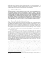
if this pair of half-vortices has a fermion in the core then we will call the state of the qubit |1i,
otherwise it is |0i. If we move (say) η3 around both η1 and η2 , the state acquires some phase if the
core is empty, but it acquires that phase plus an extra phase factor of −1 if the core is occupied by
a fermion. If we instead move η3 around only one of η1 or η2 , then the state of the qubit flips (that
is, an empty vortex acquires a fermion, or a full one loses its fermion)9 .
Das Sarma, Freedman and Nayak [2] have proposed using these braiding rules alone (without taking advantage of the fusion rules explicitly) to at least determine whether the ν = 5/2 state
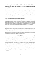
is non-Abelian via an interference experiment10 . The idea of the experiment is to localize η1 and
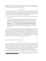
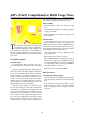
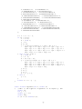
η2 on antidots in a three quantum point contact (qpc) interference device (see Figure 2.1). Two
tunneling paths, at qpc-1 and qpc-3, would interfere. Assume for now the interference is positive:
σxx ∝ |t1 + it2 |2 . Next, η3 would be allowed to controllably tunnel across qpc-2, which should flip
the qubit and change the sign of the interference to σxx ∝ |t1 − it2 |2 . If the interference changes
as a result of the braid operation, then the ν = 5/2 state must be non-Abelian. This proposal is
exceptionally ambitious. It is however, the proposal that motivated our own experimental effort at
ν = 5/2.
Shortly after Das Sarma, Freedman and Nayak published their proposal, several other authors published modifications that make the experiment simpler but still capable of probing nonAbelian statistics of the ν = 5/2 state [3–6]. These other proposals all require the use of gates to
manipulate the ν = 5/2 state, and typically call for tunneling of quasiparticles between the ν = 5/2
edge states.
In the remaining few sections of this introduction, the tone will become much more experimental. I will review prior experimental work at ν = 5/2, discuss our more immediate experimental goals and results, and provide a brief outlook for future experiments.
9 The
truly goal-oriented researcher would call this operation a not gate.
10 As far as I know, nobody has proposed a way to take advantage of the fusion rules. Presumably a scheme with fusion
would eliminate the need to measure the system using interference.
12
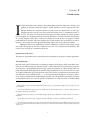
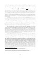
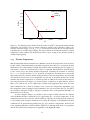
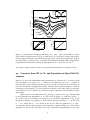
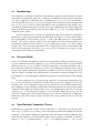
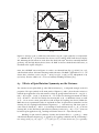
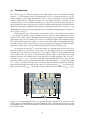
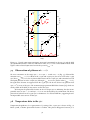
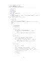
1
2
3
Figure 2.1: Artist’s rendering of the device proposed by Das Sarma, Freedman and Nayak. The
current flows along the edges as indicated by arrows. Tunneling occurs at the qpcs labeled 1 and
3. The two tunneling paths will interfere either constructively or destructively, influencing the
conductance. The two half-flux quasiparticles of a qubit are localized on the two stars. Another
half-flux may tunnel at qpc 2. If the ν = 5/2 state is non-Abelian, this braiding operation will
switch the interference from constructive to destructive or vice versa.
2.3
Prior experimental work
In 2005, when Das Sarma, Freedman and Nayak [2] published their method to experimentally
study the non-Abelian statistics of the ν = 5/2 state, it immediately prompted several experimental
groups (including our group, of course) to begin studying the manipulation and measurement of
the ν = 5/2 state in mesoscopic devices. In terms of studying 5/2 with gates or in etched structures
small enough to observe tunneling between edge states, I am not aware of any published prior
experimental work. However, a tremendous amount of experimental work has been done to study
the ν = 5/2 state in the bulk, and to study other fqhe states using qpcs.
Prior ν = 5/2 experiments
The first quantized Rxy plateau at ν = 5/2 was observed by Willett and coworkers in 1987 [45]. At
that time, the discovery of an even-denominator fqhe state was somewhat of a surprise (although
Halperin, four years earlier, had already proposed the possibility of boson-like bound-electron
pairs [57]), and there was certainly no consensus then (or even now) about the physics of the state.
Over the two decades since then, the quality of available 2deg GaAs/AlGaAs heterostructures
has improved tremendously. The measured 5/2 energy gap (∆) has increased from ∆ = 52 mK
in 1988 [58] to more than 500 mK today [2]. At the present time, the quality of the 2deg has
become so good that the ν = 5/2 state is just one (relatively stable) phase out of many exotic
phases that can be observed between ν = 3 and ν = 2 [59]. Important works using tilted magnetic
13
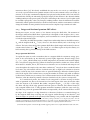
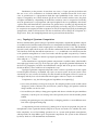
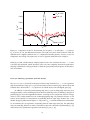
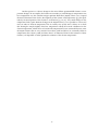
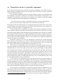
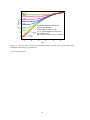
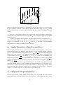
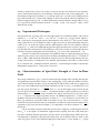
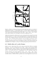
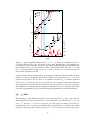
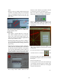
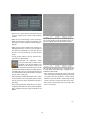
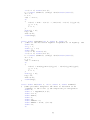
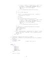
RD at ν=5/2.
RD at ν=2.
0.503
R h/e
2
0.502
0.501
0.500
0.499
Offset +0.1 h/e
-15
-10
-5
0
Idc (nA)
5
10
2
15
Figure 2.2: Comparison of the I-V characteristic for an iqhe (ν = 2) and fqhe ν = 5/2 plateau.
RD is, in fact, dV/dI, the differential resistance. The iqhe state shows ohmic behavior, while the
fqhe behavior is highly nonlinear due to a complicated tunneling density of states at very low
temperature and voltage. The fqhe curve is seen to approach ohmic behavior at high Idc .
fields [60, 61] and variable-density samples [62] have led to the conclusion that the ν = 5/2 state
is probably spin-polarized, which tentatively rules out some competing theoretical explanations.
Ongoing experimental work [63] is likely to clarify the spin-polarization properties of the bulk 5/2
state even further.
Prior fqhe tunneling experiments (and some theory)
The use of a qpc to selectively backscatter fractional edge channels for ν < 1 was experimentally demonstrated as long ago as 1990 by Kouwenhoven and coworkers [64]. Camino, Zhou and
Goldman have observed the ν = 11/3 plateau in an etched device with self-aligned gates [65].
In addition to selectively backscattering edge states, a qpc can bring edge states into close
enough proximity to allow tunneling between them. For fqhe edge states, including 5/2 [66], this is
predicted [67] to cause the longitudinal resistance to diverge at zero temperature and zero voltage,
when all of the current tunnels into the counterpropagating edge. Of particular relevance to our
results, the theoretical I-V characteristic for tunneling between fqhe edge channels has a very
distinct shape [68], illustrated in Figure 2.2. The peak at Idc = 0 and the minimum at intermediate
Idc are understood to be signatures of tunneling between fqhe edge states [68]. For iqhe edges
states the tunneling behavior is ohmic. This behavior has been observed experimentally [69, 70],
and found to be in quantitative agreement with theory [29, 68, 71, 72].
14
2.4
Impact of this work and future directions
The effort to probe the statistics of the ν = 5/2 fqhe state has just begun. Prior to our work
(described in detail in Chapter 7), only bulk experiments on the ν = 5/2 state had been reported. In
fact, it was not known whether the ν = 5/2 state could even exist in a confined area, since the state
exists only by virtue of exceptionally delicate bulk many-particle correlations. Furthermore, it was
not known whether the specialized, ultra-high mobility GaAs/AlGaAs samples that support the
ν = 5/2 state (which have δ-doping layers both above and below the 2deg, see Appendix D) could
be processed without destroying the ν = 5/2 state, and whether such material was even gateable
using standard top-gate depletion techniques. Furthermore, although the ν = 5/2 state exhibits all
the behaviors of a compressible quantum Hall state, there was no experimental evidence that it
would definitely even support an edge channel capable of tunneling. Although the existence of
edge channels has never been in serious doubt, experimental confirmation is always important,
especially since the theoretical proposals to probe the statistics at ν = 5/2 require interference of
edge channels. Our experiments have addressed all of these points.
We found that our standard nanofabrication procedure did degrade the 2deg, but I developed an improved procedure to fabricate Hall bars and nanoscale devices without affecting the
wafer mobility or the quality of ν = 5/2 features. My complete nanofabrication recipe is printed in
Appendix C.
Another difficulty was that the growth parameters that produce these remarkable bulk materials are not necessarily compatible with easy gating. We tested quite a few wafers with good
ν = 5/2 features that were ungateable due to switching noise, giant gate drift, unmanageable hysteresis and irreversibility of applied gate-voltage11 . Eventually, we found a wafer that happened
to have both manageable gates and good bulk ν = 5/2 features. Unfortunately, at this time there is
no clear correlation between growth parameters and useable gates, although some pattern could
emerge as we test even more wafers. Incidentally, we also found that all materials were utterly
ungateable after illuminating the (cold) sample with an infrared led12 .
We have observed plateau-like features near ν = 5/2 and ν = 21/3 in qpcs with 1.2 µm and
0.8 µm spacings between the gates. At temperatures above about 18 mK, the plateaus disappear.
Below this temperature, the resistance of the plateau-like feature is higher than the bulk-quantized
value of 0.4 h/e2 , and increases as temperature is decreased. The Idc traces near ν = 5/2 and
ν = 21/3 in these qpcs exhibit a characteristic shape, showing a peak in resistance at Idc = 0 nA,
a minimum near Idc = 1.2 nA, and approaching a constant value at higher currents. These observations are consistent with the formation of a gapped, incompressible fqhe state in the qpc at
these filling fractions, with qpc-induced tunneling between the edge states. In a qpc with 0.5 µm
spacing between the gates, we do not observe a plateau-like feature at any temperature, and the
Idc characteristic is flat for the entire range between ν = 3 and ν = 2. This suggests that in our
sample no incompressible states form in this qpc, probably due either to confinement or the effects of decreased electron density. All of these measurements were carried out in a magnetic field
range where the bulk filling fraction was on the iqhe ν = 3 plateau, while the filling fraction in
the qpc was tuned to lower values via the gate voltage.
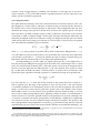
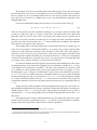
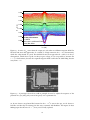
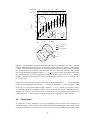
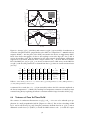
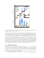
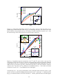
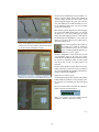
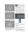
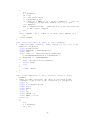
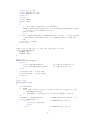
Interestingly, we find that there is a peak in resistance at zero Idc for the ν = 5/2 state, not a
dip (see Figure 2.3). In the language of an interesting paper by Roddaro [70], this means that the
5/2 state behaves like a particle tunneling state, not a hole tunneling state. Furthermore, although
11 All
"irreversible" gate behavior was reversible upon warming and re-cooling the device.
12 We
did find, consistent with the literature, that illumination improved the bulk fqhe properties of the material
15
0.430
0.420
RD (h/e²)
0.410
0.400
0.390
0.380
0.370
775 nm point contact.
iac=.855nA
0.360
Each trace is a different B field
Traces Not Offset
-12
-8
-4
0
idc (nA)
4
8
12
Figure 2.3: A series of Idc curves from the 0.8 µm qpc, each taken at a different magnetic field. The
The thick red curve that approaches R = 0.375 h/e2 at high current is the ν = 21/3 characteristic,
which has a dip instead of a peak. The thick black curve that approaches R = 0.4 h/e2 is the 5/2
characteristic, which shows a peak. At this qpc gate voltage, it was not possible to measure the
ν = 21/3 characteristic, because the required magnetic field would take the bulk filling fraction
away from ν = 3.
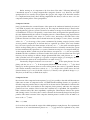
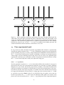
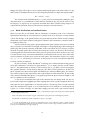
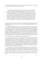
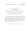
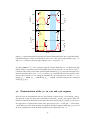
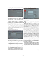
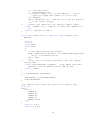
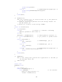
Figure 2.4: A prototype device that could in principle be used to adjust the steepness of the
potential in a qpc (using only some of the gates) or in a quantum dot.
we do not observe any plateau-like features for the ν = 22/3 state in the qpc, we do observe a
hole-like zero-bias dip in resistance for this state, consistent with Roddaro. The impact of these
findings upon the theories of ν = 5/2 has yet to be fully explored.
16
Future directions
The opportunities for continued experimental work on fqhe states in general and the ν = 5/2 state
in particular are myriad. More detailed studies of the tunneling properties of the ν = 5/2 state,
especially at various temperatures, should be carried out. The use of extra gates in and around a
qpc or quantum dot to adjust the steepness of the potential profile or increase the electron density
inside the qpc (so that, for example, the qpc can have ν = 5/2 while νbulk = 2) could possibly
help stabilize the ν = 5/2 state within a qpc or quantum dot. For example, see Figure 2.4. It has
been suggested [73] that in some cases fqhe states could be stronger in a confined area than in the
bulk of certain "dirty" samples, if the filling fraction of interest could be restricted to an area (ie,
in a qpc or dot) smaller than the scattering length. Devices with more than one tunneling gate
could be used to test the theoretical interference predictions. Finally, high-bandwidth studies of
the shot-noise of the ν = 5/2 state [74] could turn out to be the best way to probe the statistics of
fqhe states, including ν = 5/2.
2.5
Techniques
In this section I discuss some non-obvious experimental details, especially the issue of electron
temperature in quantum Hall measurements.
2.5.1
Refrigerator and wiring
We used a Frossati dilution refrigerator with a mixing-chamber base temperature of 5 mK, as
measured using a calibrated RuO2 resistor mounted on the mixing chamber. Coaxial cable was
used for electrical wiring from a break-out box, to the refrigerator, and all the way down to Frosatti
silver-epoxy filters. The filters were mounted in the bulkhead of a shielded chamber, thermally
anchored at the mixing chamber. Within this chamber, the sample was mounted in a socket on
a silver cold-finger attached to the mixing chamber. The socket was electrically connected to the
filters with copper wire.
2.5.2
LED
Within this chamber we mounted an infra-red light emitting diode. We used digikey part number
516-1262-ND, "Emitter IR 5mm 875nm." We were able to flash this led at base temperature, although the length of time of the flash was limited to about 5 minutes to avoid crashing the mixing
chamber due to excess heat. Attempts to mount the led at the ivc bulkhead (effectively at the
liquid helium bath), bringing the light to the sample with a fiber optic, were unsuccessful. The
fiber optic cable was difficult to thermally anchor at the mixing chamber, and therefore heated the
sample. Also, the efficiency of the fiber optic coupling, even though we physically mounted the
fiber optic into the led, was poor, and the desired effect of improving the 2deg mobility was never
achieved using this method.
With the led mounted directly shining on the sample, we used a Keithley 2400 to source 3.0
to 3.6 V with the current compliance limited. Once the led reached its steady-state temperature,
the current at 3.0 V was about 3 mA. We were able to achieve significant improvements in the
sample mobility using the led, although it made the gates unusable.
17
Center of 5/2 dip, bulk.
ln(Rxx)
Linear fit
-5.6
-6.0
ln(Rxx)
-6.4
-6.8
-7.2
-7.6
-8.0
0.025
0.050
1/T
0.075
0.100
Figure 2.5: An Arrhenius plot of ln( Rxx ) from the center of a bulk 5/2 dip against mixing chamber
temperature. The red line is a fit to a portion of the data, and the slope of this line is used to estimate the activation energy ∆, via Rxx ∝ e−∆/2T . The deviation from the line at low temperatures
is probably due to variable range hopping. The arrows indicate an ill-advised method to estimate
temperature, which requires that the deviation is due to poor cooling of the electrons instead of
variable range hopping.
2.5.3
Electron Temperature
With quantum Hall effect measurements it is difficult to measure the temperature of the electrons,
because unlike Coulomb blockade peak-width in quantum dots, there is no convenient absolute
thermometry. One could attempt to handle this problem using an Arrhenius plot (see Figure 2.5),
with ln( Rxx )—where Rxx measured in the center of a quantum Hall minimum—plotted against
1/TMC —where TMC is the mixing chamber temperature. Assuming the resistance is activated,
Rxx ∝ e−∆/2T , the plot of ln( Rxx ) vs 1/T should be a straight line. Assuming that at reasonably
high temperatures the electrons and the mixing chamber are the same temperature, and assuming
any deviations from the line at low temperature are due only to deviations between the mixing
chamber and electron temperature, it would be possible to estimate the actual electron temperature using the linear fit (see Figure 2.5). However, these assumptions are quite dubious, and not
likely to be valid. In fact, at low temperatures variable range hopping is likely to be the dominant contributor to Rxx , which is thought to have a power law temperature dependence [75].
The temperature where hopping becomes dominant is not even necessarily that low: for iqhe it
can already be dominant as high as 4 K [76]. So using the center of the quantum Hall dips as a
thermometer is not effective.
At lower magnetic fields, it is possible to find a region in field where the Rxx minima
of the Shubnikov-de Hass oscillations are just approaching Rxx = 0 at base temperature. As the
temperature increases, the resistance of these minima is expected to be activated, which in this case
is a reasonably good assumtion. Similarly, at low fields, the amplitude of the Shubnikov-de Hass
oscillations can be analyzed using Dingle plots [77, 78] to estimate a temperature. However, due
to the significant difference in Hall resistance between low and high field, there is no guarantee
that the low-field electron temperature is applicable to the high-field regime.
18
Another option is to observe changes in the most delicate quantum-Hall features as temperature changes. In our samples, the feature most sensitive to small changes in temperature near
base temperature was the reentrant integer quantum Hall effect (riqhe). There is no accepted
theoretical functional form for the development of this feature with temperature [79], but qualitatively the development of this feature is well known [59, 80, 81]. Very small changes in the
temperature lead to quite dramatic changes in the riqhe features, so it is possible to at least rank
traces in order of electron temperature. This is actually very useful, since it allows us to check
that heating the sample slightly from base temperature actually does make a difference in the
electron temperature, which shows at least that the temperature has not saturated. However, since
the riqhe features that are very sensitive from about 30 mK and below are essentially absent at
temperatures above about 50 mK, and since there is no functional form for the resistance of these
features, it is impossible to make quantitative estimates of the electron temperature.
19
20
Chapter
3
Introduction to the spin-orbit coupling experiments
In this chapter, I begin with a brief introduction to the effects of spin-orbit coupling upon transport in a two-dimensional electron gas (2deg), followed by a brief introduction to conductance
fluctuations and random matrix theory. Then, I discuss the place of my work in this field of study.
Finally, I record some of our techniques from these experiments.
3.1
3.1.1
Theoretical background
Spin-orbit coupling
Spin-Orbit coupling means that an electron’s spin can become coupled to its motion as it moves
around in the 2deg1 . The way this happens is quite a fascinating relativistic effect: an electric field
in the laboratory feels like a magnetic field in the rest frame of the (fast-moving) electron. From
special relativity [82], the electron feels effective an magnetic field
BSO = −(
v
× E)(1 − v2 /c2 )1/2
c
(3.1)
(where v is the velocity of the electron) which causes the spin to Larmor precess via s · BSO . So we
see a magnetic field (or at least an effective magnetic field) creeping into the system even when
we did not explicitly apply one. What is really interesting, though, is that this effective field does
not lift Kramer’s degeneracy the way a normal magnetic field would, because spin-orbit coupling
does not break time reversal symmetry.
For an electron in a GaAs/AlGaAs heterostructure, spin-orbit coupling can arise via three
different mechanisms.
The first two mechanism are due to the GaAs itself: the polar bond between the gallium
and arsenic atoms is asymmetric and produces an electric field which produces a spin-orbit contribution known as the Dresselhaus term. Silicon, by contrast, is inversion symmetric (it only has one
kind of atom) so does not exhibit Dresselhaus-type spin-orbit coupling. Dresselhaus [83] wrote
down the full Hamiltonian for 3d conduction band electrons with this type of interaction, but in
2d only two terms survive. One term is linear in the momentum (k) of the electron (note that
√
k = 2πn is related to the electron density, which we can control experimentally via a top-gate):
(1)
HD = α1 (−σx k x + σy k y ),
(3.2)
and one term is cubic in k:
(3)
HD = γ(σx k x k2y − σy k y k2x ).
(3.3)
The third source of spin-orbit coupling in a GaAs/AlGaAs heterointerface is the electric
field from the potential which confines the electrons to the 2d boundary. This term, called the
1 Spin-orbit
coupling is not exclusively a 2d effect the way anyons are, but I will only talk about the 2d version.
21
Rashba term [84], will not play a role in symmetrically-doped square wells where there is no net
field2 , but does contribute linearly in k for the triangular potential in a single-side-doped sample3 :
HR = α2 (σx k y − σy k x ),
(3.4)
The constants in these Hamiltonians, α1 , α2 and γ have been calculated by adding the spinorbit interaction as a perturbation to band structure calculations [85, 86], but the answers vary.
In Chapter 4 we report how we separately measured these three constants using transport. To
explain this measurement, however, I first need to introduce weak antilocalization
3.1.2 Weak localization and antilocalization
Ohm’s law feels like an old friend. Like an old friend, it sometimes needs a few corrections.
Quantum mechanically, the wave function for a particle (such as an electron in a 2deg) includes
a phase that changes as the particle follows any given trajectory. If the electron scatters (changes
momentum) several times without losing phase coherence, then interference corrections need to
be applied to Ohm’s law.
Enhanced backscattering is quite a general phenomenon when coherent waves meet a random
array of scatters: it is observed for laser light scattering in a cloudy liquid [87], radar scattering off
clouds [88], and electrons scattering off disorder in the 2deg. When the wave scatters, it follows
all kinds of random paths and on average the interference cancels out. However, all closed-loop
scattering paths that start and end at the same point are special, because there are always two ways
to scatter around a loop—forward and backwards, or forward and time reversed—that, unless time
reversal symmetry is broken, have exactly the same phase. The interference for these two paths,
ei( ϕ1 − ϕ2 ) = e0 = 1, will always be constructive. So the process for a wave to backscatter right back
to where it started is enhanced.
In phase-coherent, weakly disordered4 conductors, this enhanced backscattering process
causes the conductance to decrease by approximately e2 /h, no matter what the overall conductance is5 . This phenomenon is known as weak localization [26, 90, 91]. When at least one magnetic
flux quantum threads a closed electron trajectory, then time reversal symmetry is broken. The
phase acquired over time-reversed paths will differ by the Aharonov-Bohm phase, the interference will no longer be fully constructive, and weak localization will be lifted. This all only works
if the electrons remember their phase, so any path longer than the phase coherence length ` ϕ will
also not contribute to the localization.
So far, we have assumed that the spin of the electrons does not change much over any trajectory. If the sample has negligible spin-orbit coupling, this is often a good assumption. However,
if the spin does rotate significantly as an electron traverses a closed loop, then we need to include
this in the calculation. In Section 2.2.2, we learned that the wave function of a fermion picks up
a phase of −1 when rotated by 2π. Spin-orbit coupling can cause such a spin rotation without
2 For example, the fqhe samples discussed in Chapter 7 are double-doped square-well samples that would be expected
to exhibit negligible Rashba effect.
3 Most
4 The
of the wafers we have used for top-gate controlled mesoscopic physics have had triangular potentials.
disorder is considered weak if the conductance is about e2 /h or higher
5 To see that the magnitude of the correction is independent of the overall conductance requires a subtle argument.
For a very clear explanation, including the way this universal correction scales for larger (coherent) conductors of various
geometry, I recommend Datta’s book [89, Chapter 5].
22
breaking time reversal symmetry, and the resulting minus sign shows up in the interference6 . In
samples with strong enough spin-orbit coupling, this phase shows up in the transport: the weak
localization dip is transformed into an antilocalization peak in conductance.
3.1.3
Conductance fluctuations
Another manifestation of quantum interference, which also has a universal magnitude, is universal conductance fluctuations (ucf) [90]. The conductance of a sample is sensitive in detail to the
position of scatterers in the sample, because the interference depends in detail on the path lengths
between scattering events. Slightly changing the fermi energy of the sample, or slightly moving
some of the scatters can completely change the interference, leading to fluctuations in the sample conductance. Similarly to weak localization, these fluctuations have a universal magnitude of
about e2 /h, regardless of the overall conductance of the sample (as long as the overall conductance
is higher than about e2 /h). Datta’s book offers a very clear explanation of this universality [89].
3.1.4
Physics in the dot and random matrix theory
I turn now turn to the quantum dot [93]. Using nanoscale depletion gates, it is possible to create a
zero-dimensional confinement potential for electrons, connected to the 2d reservoirs by quasi-1d
quantum point contact (qpc) channels. The confinement causes the continuous dispersion of the
free electron gas to break up into discrete allowed energy levels, à la the particle-in-a-box problem
from introductory quantum mechanics. In this thesis, I only deal with "large" quantum dots (1 µm2
- 8 µm2 which contain roughly 100-1000’s of electrons), where the picture is more complicated. In
fact, the situation is chaotic.
The study of quantum chaos is new (only 30 years old) compared to the study of quantum
mechanics in general (about 100 years old). A technique to study the quantum chaos in quantum
dots, random matrix theory (rmt) [94, 95], was (and is) an active area of theoretical research even as
we conducted the large-dot experiments reported in Chapters 5 & 6. The exact spectrum of energy
levels of a large dot may be too complicated to write down, but according to rmt the statistical
distribution of energy level spacings is universal, depending only on the presence or absence of
symmetries of the system. Dots can be categorized by symmetry properties such as time reversal
symmetry, spin-orbit coupling and spin degeneracy, each category possessing a predictable energy
level distribution. rmt can predict certain measurable features of the chaotic system, such as the
average and variance of conductance.
The variance of conductance, which arises from the interference of multiple transport paths
through the device, is completely analogous to ucf in bulk samples. However, unlike 2d systems,
the quantum dot is in many ways an ideal place to study quantum chaos. Because the overall
conductance of the device can easily be set to a few e2 /h, the ucf represent a large fractional
change in the signal and are easy to measure. Quantum dots can be fabricated in any size, so
many of the relevant scales in the problem can be set by the experimentalist. Dots are extremely
tunable, so large statistically independent samples of the quantum chaos can be measured just by
changing a voltage. Importantly, although dots bestow significant control to the experimentalist,
they do not trivialize the problem: In fact, the combined influence of coherence, confinement,
electron-electron interactions, spin and spin-orbit coupling [96] makes the physics an extremely
rich ground for experimental and theoretical studies.
6 Because the interference is for all electron paths, the spin rotation needs to be averaged, so interference term is −1/2,
not −1 [92].
23
3.2
Perspectives on the 2d spin-orbit experiment
In this and the following section, I describe the specific contributions of my PhD research to
understanding the problems introduced in this chapter. This section deals with the 2d spin-orbit
work reported fully in Chapter 4.
The experiment described in Chapter 4 took place during somewhat of an awakening about
the importance of spin-orbit coupling in GaAs/AlGaAs heterostructures. Shortly prior to our
experiment, the prevailing view was that there essentially was no significant spin-orbit coupling
in GaAs. Quoting directly from Beenakker and van Houten [97]:
We will not discuss the effects of spin-orbit scattering or of superconducting fluctuations, since these may be neglected in [GaAs/AlGaAs heterostructures].
The beginning of the end to that attitude was an important paper by Paul Dresselhaus and coworkers [98] showing weak antilocalization in GaAs/AlGaAs heterostructures that was tunable via a
top-gate7 . Clearly, spin-orbit is not negligible in GaAs.
Even before Dresselhaus’ experiment, it was known that spin-orbit coupling and antilocalization could be important, especially in other materials such as InGaAs which have very strong
spin-orbit coupling. Hikami, Larkin and Nagaoka [99] had included a spin-orbit term in a formula
for the shape of weak localization in a magnetic field. Knap and coworkers extended the theory to
include different spin-orbit mechanisms [85], but all of these theories used a diffusive approximation, and were not actually applicable to the very clean, ballistic GaAs samples that Dreselhaus,
ourselves and others were measuring.
Meanwhile, spintronics [100, 101] (the manipulation of electron spin without destroying
phase coherence) was becoming a "hot" topic in condensed matter physics. Instead of neglecting
spin-orbit coupling, people were employing it as a key feature in devices such as the "Datta and
Das" coherent spin rotator [89] and spin-orbit-based spin-filters [102, 103].
This was the state of the field when we were doing our experiment. People wanted to use
spin-orbit coupling to make spin-transport devices, but there was no applicable theory to explain
antilocalization, one of the most easily observed effects of spin-orbit coupling, in high-mobility
GaAs heterostructures. Moreover, although the three materials-specific spin-orbit constants had
been calculated [85, 86], and measured using Raman spectroscopy [104], they had never been
separately measured using transport. Knowledge of these three constants (see Section 3.1.1) is
especially important for spintronic applications, because they affect the spin precession for electrons traveling along specific crystallographic directions; in fact, at certain densities, there could
be certain directions where there is no precession.
As far as I know, our experiment [105] was the first time that the spin-orbit strength was
tuned in situ with a gate voltage from complete weak localization to antilocalization. Moreover,
our paper included a new theory of antilocalization that was applicable to clean, ballistic (meaning
the spin-orbit length was longer than the mean free path) samples. The combination of the theory
and our gate-voltage dependent data allowed us to separately measure the contributions of the
three spin-orbit mechanisms (Rashba, linear Dresselhaus and cubic Dresselhaus).
In the years since we published our experiment [105], the interest in spintronics has continued [106], and there have been many interesting experimental advances, such as a spin laser
[107]. Theoretical proposals for new spintronic devices, such as "Electric-dipole induced spin resonance in disordered semiconductors" published this year in Nature Physics [108], appear regularly.
7 It
is surprising but apparently true that writing important papers about spin-orbit coupling is a hereditary trait.
24
Although it seems like practical applications of spintronic devices may need to wait for advances
in materials [106], especially (perhaps) magnetic semiconductors, the scientific progress spurred
by spintronic research is ongoing. For example, Schliemann, Loss and Westervelt [109] have proposed a method to study zitterbeweung—a long-standing prediction of relativistic quantum mechanics that leads to an oscillatory term in the Hamiltonian—using spin-orbit scattering in GaAs
heterostructures. Another interesting active avenue of research has to do with the importance of
Berry’s phase in spin-orbit systems [110–112], a point we also highlighted in our paper.
These papers [106, 109, 110] demonstrate one of the two main ways our paper has had an
impact on the field of spintronics. Our result is often cited in the theoretical literature when quantitative values of the three spin-orbit materials constants are required to make predictions. The second impact our paper has had is to provide a valid theory to fit other spin-orbit measurements—
mostly, it seems, in other materials systems such as InSb/InAlSb. Every so often I receive an email
like this one8 , which arrived on 19 Dec, 2006:
JeffI don’t believe we have met, however David Goldhaber-Gordon
recommended that I contact you in regards to a physics problem.
I have a group at the University of [somewhere], doing transport
measurements on InSb/InAlSb quantum wells for the last few years.
Recently we have been doing some low field measurements. InSb has
enormous spin-orbit coupling, so as you might suspect, we get a
significant anti-weak localization signal. Additionally the samples
are of relatively high mobility (>100,000 cm2 /Vs) compared to non-GaAs
systems. Some of our samples are in the ballistic regime where the mean
free path exceeds the magnetic length.
We have been trying to fit our data with the ballistic theory
introduced in a PRL on which you a co-author (PRL, 90 76807 (2003)). We
have not found this to be easy. David tells me that you were the fitting
expert for the previous gated GaAs results. I was wondering if you could
share some insights with us.
Thanks in advance.
This email simultaneously illustrates a feature of our paper and a weakness. The feature
is that ours is still essentially the only theory that is applicable in the ballistic regime for fitting
antilocalization data. The weakness is that the formulas really are a bear to work with, although I
guess they are what they are based on physics.
3.3
Perspectives on the quantum-dot experiments
In this section, I discuss the specific contributions to the literature of the quantum dot experiments
described in Chapters 5 & 6. These two chapters (and two papers [113, 114]) present results on
a single overarching topic: the study of an extremely rich many-body physics problem. The distinction between the two chapters is that Chapter 5 deals mainly with average conductance while
Chapter 6 is primarily about variance.
Just before we measured the spin-orbit properties in our 2d sample, Folk and coworkers [96]
had noticed something unexpected about ucf in a quantum dot. Folk’s experiment was designed
8 To
protect the privacy of the sender, I have removed names and places
25
to try to determine whether electron-electron interactions break spin degeneracy in a quantum
dot by applying an in-plane field. In Folk’s words [96]:
The original concept for the measurement was that if the system were spin degenerate at low field, then a large in-plane field would lift the degeneracy via Zeeman
splitting, with associated changes in the amplitude of conductance fluctuation. If, on
the other hand, spin degeneracy at low field were already lifted by interactions, then
a large parallel field would not alter spectral statistics and hence conductance fluctuation amplitude. Surprisingly, we find that the conductance fluctuations are indeed
suppressed by a strong parallel field (suggesting degeneracy at low field), but in many
cases by a significantly greater factor than can be understood in terms of a simple
breaking of spin degeneracy. At the end of the paper, we suggest a possible explanation for this large suppression as resulting from field-dependent spin-orbit scattering.
Something unexpect was going on, and the cause was probably spin-orbit coupling. Halperin and
coworkers published a theory paper (the very next letter after Folk) supporting spin-orbit as the
explanation [115].
Meanwhile, Dominik and I had a chip with strong, well-studied spin-orbit coupling in the
’fridge. We pulled the chip, Dominik made quantum dots, and we got to work trying to sort out
what was going on. As we were measuring, Aleiner and Fal’ko published a paper that expanded
upon Folk and Halperin’s theory that spin-orbit coupling was involved; in fact, they identified
"all possible symmetry classes which arise from the interplay between SO coupling and Zeeman
splitting in a disordered or chaotic semiconductor quantum dot and describe all the physically
achievable parametric dependencies treated as crossovers between distinct symmetry classes,"
[116]. In other words, they massively expanded the applicability of random matrix theory. Our
work [113] provided quantitative confirmation of these theories, which represents quite an advance
in the understanding of a very complicated many-body problem in physics.
The only small detail is that our results did not agree quantitatively with the theory in fairly
high parallel magnetic fields. It turns out that this did not represent a failure of the theory, just
an opportunity to add one more detail. The same year we were measuring, Fal’ko and Jungwirth
[117] and Meyer and Alt’shuler [118, 119] published papers correcting the naive view that in-plane
fields influence only the Zeeman energy without affecting the orbital physics. In fact, the parallel
field can break time reversal symmetry and couple to the orbital motion of electrons. Adding the
Fal’ko/Jungwirth terms to the Aleiner and Fal’ko theory allowed us to understand the average
conductance and conductance fluctuations in our dots of various sizes (and with a top-gate) in
materials with strong and weak spin-orbit coupling.
Our paper, along with the theory papers I mentioned above—and of course Folk’s first
observations—helped open up an entire field where spin-orbit coupling and quantum dots are
used to understand and control spin. Theoretical and experimental papers continue to report increasingly sophisticated techniques, as exemplified by a recent Letter [120], where single-electron
resonant tunneling spectroscopy is used in conjunction with the anisotropy of spin-splitting to
measure the relative strength of Rashba and Dresselhaus spin-orbit mechanisms in a quantum
dot.
26
2.0
6
ln(f)
1.5
5
4
1.0
3
2
1
0.5
σ (1/2π² e²/h)
7
0.0
-4
-2
0
ln(x)
2
4
Figure 3.1: This is our calculation of the function C ( f , x ), the Cooperon term, in Equation 4.2.
3.4
3.4.1
Techniques
Data Acquisition
The data for the 2d paper (Chapter 4) was difficult to acquire because a typical localization feature was only about 0.1% of the overall signal. In fact, it was virtually impossible to see any
localization peaks or dips in any single magnetic field trace. In order to achieve acceptable signalto-noise ratios in finite time, we took hundreds of traces and averaged them. This turned out to
be faster—that is, we measured more statistically independent points in a given amount of time—
than turning the time constant on the lock-in way up, since the overall noise between successive
points was typically larger than the change in the signal.
We also used the transformer on the Princeton Applied Research 124 lock-in amplifiers.
Later, we spent a month ensuring the linearity of our measurements. I would tend to avoid using
the transformer in the future unless there is really no other way to take data.
3.4.2
Data Analysis
The data acquisition for the 2d paper required very careful measurements, but the data analysis
turned out to be even harder. We first tried to fit our data using existing theories [99, 122], but these
theories did not yield useful results, even though the fits looked quite acceptable, because they
were designed for diffusive samples and were not valid in our ballistic sample. Once we arrived
(with Yuli’s help) at the correct theory to use, things actually become even harder. The heart of the
theory is the Cooperon function, which is the sum of an infinite sum of several integrals. None of
them converge particularly fast. In the end, we had the idea to calculate the function only once for
a massive 2d parameter space. The result is shown in Figure 3.1. The function is at least smooth.
With such slowly converging integrals, we wanted to somehow check that our numerics were
working correctly. Fortunately, Zduniak [121] had calculated the Cooperon function in certain
limits, and our results matched his (see Figure 3.2), so we were able to proceed with confidence
that our numerical methods were correct. The full source-code used for our Cooperon calculation
27
0
C(x,f) 4π³h/e²
-1
-2
-3
Agreement between Zduniak et al.
and our XOP function:
YuliC(x,f,BS=1e-5,Qu=1e-12)
β = f-1. BS=integration bin size for P0,
Qu=cutoff for sum.
Max number of terms in sum = 1000000.
-4
-5
-6
-4
-2
0
2
4
6
ln(x)
Figure 3.2: We were able to check our numerical methods (colored points) against previously
published calculations [121] (black lines).
is listed in Appendix E.
28
Chapter
4
Gate-Controlled Spin-Orbit Quantum Interference Effects in Lateral
Transport
J. B. Miller∗ , D. M. Zumbühl, C. M. Marcus
Department of Physics, Harvard University, Cambridge, Massachusetts 02138
∗ Division of Engineering and Applied Science
Harvard University, Cambridge, Massachusetts 02138
Y. B. Lyanda-Geller
Naval Research Laboratory, Washington, D.C. 20375
D. Goldhaber-Gordon
Department of Physics, Harvard University, Cambridge, Massachusetts 02138
Department of Physics, Stanford University
Stanford, California 94305
K. Campman, A. C. Gossard
Materials Department, University of California at Santa Barbara
Santa Barbara, California, 93106
In situ control of spin-orbit coupling in coherent transport using a clean GaAs/AlGaAs 2deg
is realized, leading to a gate-tunable crossover from weak localization to antilocalization. The
necessary theory of 2D magnetotransport in the presence of spin-orbit coupling beyond the
diffusive approximation is developed and used to analyze experimental data. With this theory
the Rashba contribution and linear and cubic Dresselhaus contributions to spin-orbit coupling are
separately estimated, allowing the angular dependence of spin-orbit precession to be extracted at
various gate voltages.
[ This chapter is published in Phys. Rev. Lett. 90, 76807 (2003) ]
29
4.1
Introduction
An important component along the path toward realizing quantum “spintronic" devices [100, 101]
is a structure that allows manipulation of electron spin without destroying phase coherence. Spinorbit (SO) coupling has been the focus of recent studies because of its potentially useful role in
coherent spin rotators [89], spin interference devices [123], and spin-filters [103, 124]. The mechanisms by which SO coupling affects transport [98, 99, 122, 125] have recently been considered in
the context of Aharonov-Bohm (AB) phase and Berry phase [113, 116, 123, 126–129], underscoring the richness of the underlying physics. The results in this and other recent experiments [130]
cannot be explained without considering these AB-like effects.
The conductivity of low-dimensional systems shows signatures of quantum interference
that depend on magnetic field and SO coupling [26, 90, 99, 122, 131]. In particular, constructive
(destructive) backscattering associated with pairs of time-reversed closed-loop electron trajectories
in the absence (presence) of significant SO interaction leads to negative (positive) magnetoresistance effects known as weak localization (antilocalization). Antilocalization is the paradigmatic
experimental signature of SO coupling in phase coherent electronic systems [125].
In this Letter, we demonstrate in situ control of SO coupling in a moderately high mobility
GaAs/AlGaAs two-dimensional electron gas (2deg), inducing a crossover from weak localization
(WL) to antilocalization (AL) as a function of an applied top-gate voltage (see Figure 4.1). Theory
beyond the diffusive approximation must be used to extract gate-voltage-dependent SO parameters from magnetotransport when the SO precession frequency becomes comparable to the inverse
transport scattering time (τ −1 ) as occurs here, and when the magnetic length becomes comparable
to the mean free path. Such a theory, which also takes into account AB-like spin quantal phases
and spin-relaxation [132], is developed here and used to estimate separately the various SO terms
(Rashba, linear and cubic Dresselhaus, defined below) over a range of gate voltages, ranging from
WL to AL.
4.2
Previous Theory and Experiments
Conventional WL theories assume SO times much longer than transport scattering times [99, 122,
128] and so cannot be applied to clean materials such as high-mobility 2degs. Previous theories
that go beyond the diffusive approximation do not treat SO [133, 134], or treat it only as spinrelaxation [121, 135] without accounting for Berry phase effects which play a crucial role, as we
show here.
Previous experiments in which SO rates are measured using WL/AL in a gated GaAs heterostructure have not reported in situ gate control [98, 136, 137]. Very recently, Koga et al. [102]
demonstrated gate controlled SO coupling in InGaAs heterostructures using WL/AL, but did not
report a full crossover from WL to AL in any single sample. We know of no previous study in
which an in situ crossover from WL to AL is demonstrated. Modification of Rashba SO coupling
using gated quantum wells has been observed using beating patterns in Shubnikov-de Haas oscillations in InGaAs [138, 139], InAs/AlSb [140] and HgTe [141]. Gate controlled SO coupling in
GaAs 2D hole systems [142–144] has also been investigated using beating of Shubnikov-de Haas
oscillations. The angular variation of SO coupling in GaAs quantum wells has been measured
using Raman scattering [104], but to our knowledge has not been extracted from transport data.
30
4.3 Theory of Two-Dimensional Magnetotransport with SpinOrbit Coupling beyond the Diffusive Approximation
2 2
The Hamiltonian for conduction band electrons in a [001] 2deg is H = h̄2mk∗ + (σ · Ω), where m∗ is
the effective mass, k = |k| (k = (k x , k y )) is the in-plane wave vector, σ = (σx , σy ) is the Pauli spin
operator and Ω = (Ω x , Ωy ) is the total SO frequency. Ω = Ω D1 + Ω D3 + Ω R can be written as the
vector sum of linear (Ω D1 ) and cubic (Ω D3 ) Dresselhaus terms and the Rashba term (Ω R ),
Ω D1
ΩR
Ω D3
= α1 −x̂k x + ŷk y /h̄,
(4.1a)
= α2 (x̂k y − ŷk x )/h̄,
(4.1b)
=
γ(x̂k x k2y
− ŷk2x k y )/h̄.
(4.1c)
where γ arises from the lack of inversion symmetry of the GaAs crystal, while α1 = γhk2z i also
depends on the thickness of the wave function in the quantization direction. The Rashba coefficient
α2 depends on the potential profile of the heterointerface. In fitting the data below, we assume
the effect of gate voltage, Vg , on Ω (≡ |Ω|) is through the carrier density, n = k2 /2π. Good
agreement between theory and experiment (Figure 4.2) supports this assumption, as do previous
studies of SO coupling in single-interface heterostructures [85]. Although α2 can be treated as
directly proportional to a uniform electric field [145], the magnitude of α2 in a single-interface
heterostructure originates mainly from the band-offset at the heterointerface, which is essentially
independent of Vg [86, 140].
The symmetry of the linear (in k) SO terms, Ω D1 and Ω R , allows these terms to be represented as a spin-dependent vector potential A that affects the orbital motion and phase of
electrons, σ · (Ω D1 + Ω R ) ∝ k · A [116, 123, 126–129]. That is, the linear terms affect electronic
interference as a spin-dependent AB-like effect. In contrast, the cubic term, Eq. (1c), upon removing terms with the symmetry of Eq. (1a), only causes spin relaxation in the diffusive regime
(although it also can produce AB-like effects in the quasi-ballistic regime [123]).
To develop the theory of 2D magnetotransport with SO coupling beyond the diffusive
approximation [132], we follow Refs. [133–135], which treat the quasi-ballistic case ` B < `
√
(` B = h̄/2eB is the magnetic length and ` is the transport mean free path) without spin-orbit
coupling. The approach is to introduce an operator P = GeR+ω (r1 , r2 , σ1 ) GeA (r1 , r2 , σ2 )h̄/2πντ for
the probability of an electron to propagate both forward and backward along a path segment from
r1 to r2 , where G R (G A ) are single-electron retarded (advanced) Green functions, σ1(2) are the Pauli
spin operators for particle moving forward (backward), ν is the density of states per spin, and τ
is the scattering time. The interference contribution from the nth traversal of a closed path is given
by the trace of ( P)n . In the presence of SO coupling of the form in Eq. (4.1), formulas in [134]
remain valid once a summation over spins is included in the trace.
Introducing the total spin of interfering partial waves, S = σ1 + σ2 , we write Tr [( P)n ] =
− ( P0 )n ], where operators P0 and P1 describe singlet (S = 0) and triplet (S = 1) contributions. To calculate Tr [( P0(1) )n ], we diagonalize P0(1) . We find that when Ω D1 and Ω R are taken into
account, P0(1) has the same eigenfunctions as the Hamiltonian H for particles with charge 2e, spin
1
n
2 Tr [( P1 )
2
h̄
2
S and spin frequency 2Ω: H = 2m
∗ ( k − 2eA em + 2eA S ) , where A em is the vector potential associ∗
ated with the applied perpendicular magnetic field, B, and AS = m 3 (−α1 Sx − α2 Sy , α2 Sx + α1 Sy )
2eh̄
is the SO vector potential. For S = 0, the eigenstates are Landau levels for a charge 2e particle in the magnetic field B, analogous to the spinless problem [135]. For S = 1, eigenstates of
H and P1 in general require a numerical solution, although analytic solutions exist when either
31
α1 or α2 equals zero [132]. An analytic solution is found when both α1 and α2 may be nonzero,
when ` B < λso , where λso = (2α1(2) m∗ /h̄2 )−1 is the distance over which spin rotates appreciably
(if ` > λso ) or dephases (if ` < λso ) due to spin AB-like effects. Performing a unitary transformation H → H̃ = U † HU, with U = exp (−ieAS · r), and expanding in coordinates, we find
2
2
3
h̄
2
2
2
∗2
H̃ = 2m
∗ ( k − 2eA em + Sz a ) , where a = Heff r × ẑ/ (2h̄ ), and Heff = 2( α2 − α1 ) m /eh̄ is the
effective SO field. P1 can then be block-diagonalized for each m (m = 0, ±1) using the Landau
basis for particles with charge 2e in the magnetic field B − mHeff . Thus, the effect of Ω D1 and
Ω R is to produce spin quantal phases of the AB type [116, 123, 126–129]. Higher expansion terms
to H̃ describe spin flip processes and can be taken into account by introducing a spin relaxation
time τso and its corresponding field scale Hso = h̄τ/(2e`2 τso ). The resulting quantum interference
contribution takes the form [132],
"
#
e2
(4.2)
∆σ( B) = − 2
∑ C(x1m , f1m ) − C(x00 , f00 )
4π h̄ m=−
1,0,1
P3 ( f
)
N Sm
where xSm = ( B − mHeff )/Htr describes the AB dephasing in Heff , C ( x, f Sm ) = x ∑∞
N =0 1− PN ( f Sm ) ,
R∞
PN ( f Sm ) = y 0 exp(−y f Sm t − t2 /2) L N (t2 )dt, L N (z) are Laguerre polynomials, y = (2/| x |)1/2 ,
and Htr = h̄/(2e`2 ). The dephasing factors f Sm are given by f 1±1 = (1 + ( H ϕ + Hso )/Htr ); f 00 =
(1 + H ϕ /Htr ); f 10 = (1 + ( H ϕ + 2Hso )/Htr ), where H ϕ = h̄/(4eL2ϕ ) and L ϕ is the phase breaking
length.
Equation (4.2) does not include all B-dependent interference terms, notably excluding
Cooper-channel contributions due to electron-electron interactions [90] and a reduction of WL
due to electron diffraction effects [133]. Also, in an attempt to capture the effects of cubic
∗
terms on Heff and Hso , we introduce an effective vector potential A∗S = AS + γ m 2 (k y 2 , −k x 2 ) ∼
AS + γ
m∗
( k2 , − k2 )
2eh̄2
eh̄
which leads to an effective SO field,
∗
Heff
= 2(α22 − α21 + 2πnα1 γ − π 2 γ2 n2 )m∗ 2 /eh̄3 .
(4.3)
∗ , which corresponds in the present experiment to B
Equation (4.2) is applicable when B > Heff
between 20-100 µT depending on Vg (see Figure 5.2). We have confirmed that fitting only to data
∗ gives, within error bars, the same results as fitting over the entire measured range
where B > Heff
of B.
Modification of the commutator [k + 2eA∗S , r] by A∗S induces spin flipping terms ∼ γk3 /4 in
∗ = 1 π 2 m∗ 2 γ2 n2 /eh̄, using its expression
the transformed Hamiltonian H̃∗ . The corresponding Hso
36
in the diffusive regime.
4.4
Experimental Details
We now turn to a discussion of the experiment. Three similarly fabricated samples made on three
separate heterostructure materials were measured, all showing qualitatively similar behavior. The
sample for which data is presented consists of a GaAs/AlGaAs heterostructure grown in the [001]
direction with double δ-doping layers set back 143 Å and 161 Å from the 2deg and a total distance
of 349 Å from the surface to the 2deg. A 200 µm wide Hall bar with 700 µm between voltage
probes was patterned by wet etching. A lithographically defined Cr/Au top gate was used to
control density and mobility in the Hall bar over the range n = 1.4-7.0 ×10¹⁵ m−2 and µ = 3.631 m2 /Vs. Measurements were made in a 3 He cryostat at temperature T = 300 mK using ac
lock-in techniques with bias currents ranging from 50 to 500 nA (depending on the gate voltage).
32
-1
30
-240 mV
20
10
0
+200 mV
-20
0
20
B⊥ (mT)
+100 mV
Δσ (MΩ)
-1
10
(a)
Δσ (MΩ)
20
0
-10
0 mV
-50 mV
-100 mV
-20
-150 mV
n (10
-1
10
σ (kΩ)
2
m )
20
2
4
0.0
B⊥ (mT)
μ (m /V·s)
6 (b)
30
-2
-0.2
15
-0.4
0
-200
0
Vg (mV)
0.2
30
(c)
20
10
0
200
0.4
-200 -100
0
100 200
Vg (mV)
Figure 4.1: (a) Experimental magnetoconductance, ∆σ = σ( B) − σ(0), (circles) offset for clarity,
along with three-parameter fits to Eq. (4.2) (solid curves) for several gate voltages. Inset: Experimental magnetoconductance data for the most negative gate voltage, showing pure WL. (b) Density and mobility as a function of Vg , extracted from longitudinal and Hall voltage measurements.
(c) Experimental conductivity, showing strong dependence on Vg . Note that ∆σ ∼ 10−3 σ.
At each gate voltage, the bias current was experimentally determined not to affect the results.
4.5 Crossover from WL to AL and Separation of Spin-Orbit Parameters
Figure 4.1 (a) shows the longitudinal magnetoconductance as a function of Vg . A crossover from
pure WL (Figure 4.1(a), inset) at Vg = −240 mV to essentially pure AL at Vg = +250 mV is
observed. This crossover demonstrates that a gate can be used to control SO over a wide range, as
pure WL corresponds to negligible SO rotations within the phase coherence length L ϕ , while AL
corresponds to spin rotations & 2π. The solid curves in Figure 4.1(a) are fits of Eq. (4.2) with three
∗ , and H ∗ . H is fixed at each gate voltage by measured values of density
free parameters, Hφ , Hso
tr
eff
and mobility.
∗ and H ∗ as a function of n2 . H ∗ is well described
Figure 4.2 shows extracted parameters Hso
so
eff
by the predicted linear dependence on n2 , with a best fit (Figure 4.2, solid line) giving γ =
∗ is well
31 ± 3 eVÅ3 with zero y-intercept (see Equation (4.1c)). The density dependence of Heff
described by Equation (4.3), (Figure 4.2, dotted curve), giving fit parameters γ = 28 ± 4 eVÅ3 ,
α1 = 4 ± 1 meVÅ and α2 = 5 ± 1 meVÅ. In this way, the three SO parameters α1 , α2 , and γ
are separately obtained from transport measurements by explicitly making use of the density
∗ and H ∗ . Extracted values of H correspond to dephasing times in the range
dependence of Heff
ϕ
so
33
100
8
80
40
*
*
2
H so
20
*
H eff
0
*
60
4
H eff (μT)
H so (μT)
6
0
10
20
30
2
15
-2 2
n (10 m )
40
0
50
∗ (filled circles) and H ∗ (open squares), as extracted using
Figure 4.2: Spin-orbit effective fields, Hso
eff
∗ (dotted
Eq. (4.2), plotted as a function of sheet density squared. The best fit of Eq. (4.3) to Heff
∗
curve) is used to extract γ, α1 and α2 . Alternatively, the best linear fit to Hso (solid line) is used to
extract γ.
τϕ ∼ 0.1-1.0 ns at 300 mK, which decrease by more than an order of magnitude as temperature
∗ and H ∗ do not depend on temperature over this
is increased to 2.5 K. Within the error bars, Hso
eff
temperature range.
Figure 4.3(a) displays the magnitudes of the three spin-orbit terms as functions of Vg , n,
and µ, determined using Eq. (4.1) and the extracted values of α1 , α2 , and γ. Plotted are values
along the [110] direction, φ ≡ tan−1 (k y /k x ) = π4 , where Ω D3 is maximum. Error bars indicate
uncertainties in the fitting procedure and noise in the data.
4.6
Angular Dependence of Spin Precession Rates
The total spin precession rate, Ω, is plotted as a function of the direction, φ, of the electron
momentum in Figure 4.3(b). While for most directions Ω is an increasing function of density,
7π
it is seen to decrease with increasing density near φ = 3π
4 and 4 . The linear Dresselhaus and
Rashba terms (Ω D1 and Ω R ) are of comparable magnitude to each other for all densities and
jπ
in all directions. Near φ = 2 (j an integer), Ω D3 Ω D1 , Ω R and the SO is controlled by the
(2j+1)π
, the cubic term becomes comparable to or even exceeds (at high
linear terms. For φ near
4
densities) the linear terms. Depending on φ, the linear and cubic terms either add (φ ∼ π4 , 5π
4 ) or
3π 7π
subtract (φ ∼ 4 , 4 ).
∗ , 28 ± 4 eVÅ3 using H ∗ ) are in good
The extracted values for γ (31 ± 3 eVÅ3 using Hso
eff
agreement with the value 27.5 eVÅ3 from band structure calculations [85, 86]. Estimates for α1
give values for hk2z i that correspond to a wave function width of ∼ 10 nm in the ẑ direction, which
is also reasonable. The extracted α2 corresponds to a uniform [145] electric field E ∼ 10 MV/m,
using α2 = α0 eE and a value of α0 = 5.33 Å2 from a k · p model [85, 86].
4.7
Comparison with previous Theory
We note that previously existing models for WL/AL [85, 122, 128] provide fits to the data that
appear qualitatively reasonable, giving values for Hso that are ∼ 5 times higher than those found
34
μ (m 2 ⁄ Vs )
4 5
7
n ( 10 15 m –2 ) 1.5
200
(a)
10
15
2.0 3.0 4.0
20
25
30
5.0 5.5 6.0
6.5
7.0
[010]
[100]
Ω (ns)
-1
150
100
[010]
50
[100]
0
-200
(b)
-100
[010]
0
Vg (mV)
100
ΩR
ΩD1
ΩD3
200
Vg = -150 mV
Vg = 0 mV
Vg = +250 mV
[100]
200
250 (ns)-1
Figure 4.3: (a) Magnitudes of isotropic linear Dresselhaus (Ω D1 ) and Rashba (Ω R ) terms, and nonisotropic cubic Dresselhaus (Ω D3 ) term as functions of gate voltage, Vg , density, n, and mobility,
µ. Insets show theoretical dependence on momentum direction for the three terms, indicating
that the linear terms are isotropic, while the cubic term has a four-fold symmetry and is highly
anisotropic. Maximum magnitude (when φ = ( j + 14 )π) is shown for the anisotropic (Ω D3 ) term.
(b) Angular variation of Ω, the magnitude of the total SO precession vector at Vg = −150 mV
(dotted), 0 mV (dashed), and 250 mV (solid), corresponding to densities of 2.3, 5.0, and 7.0 × 10¹⁵
m−2 respectively.
using Eq. (4.2). However, these fits also lead to the unphysical result that τso < τ. Such unphysical
results are not surprising given that, for Vg > −50 mV, the SO length, v F /hΩi, is less than `, while
theory [85, 122, 128] assumes diffusive spin evolution ` λso , L ϕ . Finally we note that a theory
for arbitrarily strong SO coupling [129] may also be used to fit this data by including B via L ϕ ,
yielding values for Ω D3 and Ω D1 for all Vg ’s which agree with our estimates using Eq. (4.2) to
within a factor of ∼ 3. However, the theory in [129] does not separate Ω D1 and Ω R terms.
4.8
Conclusion
In conclusion, we have realized an in situ gate-controlled crossover from weak localization to
antilocalization in a GaAs/AlGaAs 2deg, experimentally demonstrating that spin rotation can be
strongly modulated in a clean, phase-coherent system. New theory addresses spin-orbit effects
35
in the quasi-ballistic regime and allows separate measurement of the Rashba, linear Dresselhaus,
and cubic Dresselhaus terms.
4.9
Acknowledgements
We thank I. Aleiner, H. Bruus and S. Studenikin for illuminating discussions and F. Mancoff
for device fabrication. This work was supported in part by DARPA-QuIST, DARPA-SpinS, AROMURI, and NSF-NSEC. We also acknowledge support from ONR and NSA (Y. L.-G.), NDSEG
(J. B. M.) and the Harvard Society of Fellows (D.G.-G). Work at UCSB was supported by QUEST,
an NSF Science and Technology Center.
36
Chapter
5
Spin-Orbit Coupling, Antilocalization, and Parallel Magnetic Fields
in Quantum Dots
D. M. Zumbühl, J. B. Miller∗ , C. M. Marcus
Department of Physics, Harvard University, Cambridge, Massachusetts 02138
∗ Division of Engineering and Applied Science
Harvard University, Cambridge, Massachusetts 02138
K. Campman, A. C. Gossard
Materials Department, University of California at Santa Barbara
Santa Barbara, California, 93106
We investigate antilocalization due to spin-orbit coupling in ballistic GaAs quantum dots.
Antilocalization that is prominent in large dots is suppressed in small dots, as anticipated
theoretically. Parallel magnetic fields suppress both antilocalization and also, at larger fields,
weak localization, consistent with random matrix theory results once orbital coupling of the
parallel field is included. In situ control of spin-orbit coupling in dots is demonstrated as a
gate-controlled crossover from weak localization to antilocalization.
[ This chapter is published in Phys. Rev. Lett. 89, 276803 (2002)]
37
5.1
Introduction
The combination of quantumcoherence and electron spin rotation in mesoscopic systems produces
a number of interesting transport properties. Numerous proposals for potentially revolutionary
electronic devices that use spin-orbit (SO) coupling have appeared in recent years, including gatecontrolled spin rotators [89] as well as sources and detectors of spin-polarized currents [103, 146,
147]. It has also been predicted that the effects of some types of SO coupling will be strongly
suppressed in small 0D systems, i.e., quantum dots [115, 116, 148–150].
In this Letter, we investigate SO effects in ballistic-chaotic GaAs/AlGaAs quantum dots.
We identify the signature of SO coupling in ballistic quantum dots to be antilocalization (AL),
leading to characteristic magnetoconductance curves, analogous to known cases of disordered 1D
and 2D systems [85, 98, 99, 105, 122, 125, 151]. AL is found to be prominent in large dots and
suppressed in smaller dots, as anticipated theoretically [115, 116, 148–150]. Results are generally
in excellent agreement with a new random matrix theory (RMT) that includes SO and Zeeman
coupling [116, 150]. Moderate magnetic fields applied in the plane of the 2D electron gas (2DEG)
in which the dots are formed cause a crossover from AL to weak localization (WL). This can be
understood as a result of Zeeman splitting, consistent with RMT [116, 150]. At larger parallel fields
WL is also suppressed, which is not expected within RMT. The suppression of WL is explained
by orbital coupling of the parallel field, which breaks time-reversal symmetry [117, 118]. Finally,
we demonstrate in situ electrostatic control of the SO coupling by tuning from AL to WL in a dot
with a center gate.
In mesoscopic conductors, coherent backscattering of time-reversed electron trajectories
leads to a conductance minimum (WL) at B = 0 in the spin-invariant case, and a conductance
maximum (AL) in the case of strong SO coupling [99, 122]. In semiconductor heterostructures, SO
coupling results mainly from electric fields [152] (appearing as magnetic fields in the electron
frame), leading to momentum dependent spin precessions due to crystal inversion asymmetry
(Dresselhaus term [83]) and heterointerface asymmetry (Rashba term [84]).
5.2
Previous Experiments
SO coupling effects have been previously measured using AL in GaAs 2DEGs [98, 105, 151] and
other 2D heterostructures [85]. Other means of measuring SO coupling in heterostructures, such as
from Shubnikov-de Haas oscillations [140, 153, 154] and Raman scattering [104] are also quite developed. SO effects have also been reported in mesoscopic systems such as Aharonov-Bohm rings,
wires, and carbon nanotubes [123, 130, 155–160]. Recently, parallel field effects of SO coupling in
quantum dots were measured [96, 161]. The observed reduction of conductance fluctuations in a
parallel field [96] was explained in terms of SO effects [115, 116, 150], leading to an extension of
random matrix theory (RMT) to include new symmetry classes associated with SO and Zeeman
coupling [116, 150].
5.3
Random Matrix Theory
This RMT addresses quantum dots coupled to two reservoirs via N total conducting channels,
with N 1. It assumes (γ, eZ ) ET , where γ = N∆/(2π ) is the level broadening due to escape,
∆ is the mean level spacing, eZ = gµ B B is the Zeeman energy and ET is the Thouless energy (Table 5.3). Decoherence is included as a fictitious voltage probe [116, 150, 162–164] with dimension-
38
A
¯m2
1.2
5.8
8
∆
¯eV
6.0
1.2
0.9
τd
ns
0.35
1.7
2.3
ET /∆
33
73
86
so /∆
e⊥
0.15
0.32
3.6
ekso /∆
0.04
0.33
3.1
a1 , a2
(ns)−1 T−2
6.6, 6.6
3.2, 0
1.4, 0.9
b2
(ns)−1 T−6
0.24
140
3.7
Dot area A = L1 L2 (130 nm edge depletion); spin-degenerate
mean level spacing ∆ = 2πh̄2 /m∗ A (m∗ =
√
so /∆ and eso /∆ for the fits in Figure 5.1; B2 coefficients
0.067me ); dwell time τd = h/( N∆); Thouless energy ET = h̄v F / A; e⊥
k
Table 5.1:
a1 and a2 from one and two parameter fits; B6 coefficient b2 from two parameter fit, see text.
less dephasing rate Nϕ = h/(∆τϕ ), where τϕ is the phase coherence time. SO lengths λ1,2 along
respective principal axes [110] and [11̄0] are assumed (within the RMT) to be large compared to
p
the dot dimensions L1,2 along these axes. We define the mean SO length λso = |λ1 λ2 | and SO
p
so = κ E ( L L /λ2 )2 ,
anisotropy νso = |λ1 /λ2 |. SO coupling introduces two energy scales: e⊥
⊥ T 1 2
so
so ,
representing a spin-dependent Aharonov-Bohm-like effect, and ekso ∼ (( L1 /λ1 )2 + ( L2 /λ2 )2 )e⊥
so
so
providing spin flips. AL appears in the regime of strong SO coupling, (e⊥ , ek ) γ̃, where
γ̃ = (γ + h̄/τϕ ) is the total level broadening. Note that large dots reach the strong SO regime
at relatively weaker SO coupling than small dots. Parameters λso , τϕ , and κ⊥ (a factor related to
trajectory areas) are extracted from fits to dot conductance as a function of perpendicular field,
B⊥ . The asymmetry parameter, νso , is estimated from the dependence of magnetoconductance on
parallel field, Bk .
The quantum dots are formed by lateral Cr-Au depletion gates defined by electron-beam
lithography on the surface of a GaAs/AlGaAs heterostructure grown in the [001] direction. The
2DEG interface is 349 below the wafer surface, comprising a 50 GaAs cap layer and a 299 AlGaAs
layer with two Si ffi-doping layers 143 and 161 from the 2DEG. An electron density of n ∼
5.8 × 10¹⁵ m−2 1 and bulk mobility µ ∼ 24 m2 /Vs (cooled in the dark) gives a transport mean free
path `e ∼ 3 ¯m. This 2DEG is known to show AL in 2D [105]. Measurements were made in a 3 He
cryostat at 0.3 K using current bias of 1 nA at 338 Hz. Shape-distorting gates were used to obtain
ensembles of statistically independent conductance measurements [165] while the point contacts
were actively held at one fully transmitting mode each (N = 2).
5.4 Antilocalization and Confinement Suppression of Spin-Orbit
Effects
Figure 1 shows average conductance h gi, and variance of conductance fluctuations, var( g), as a
function of B⊥ for the three measured dots: a large dot (A ∼ 8 µm2 ), a variable size dot with
an internal gate (A ∼ 5.8 µm2 or 8 µm2 , depending on center gate voltage), and a smaller dot
(1.2 µm2 ). Each data point represents ∼ 200 independent device shapes. The large dot shows AL
while the small and gated dots show WL. Estimates for λso , τϕ and κ⊥ , from RMT fits are listed
for each device below the micrographs in Figure 5.1 (see Table 5.3 for corresponding e⊥ and ek ).
When AL is present (i.e., for the large dot), estimates for λso have small uncertainties (±5%) and
give upper and lower bounds; when AL is absent (i.e., for the small and gated dots) only a lower
bound for λso (−5%) can be extracted from fits. The value λso ∼ 4.4 µm is consistent with all dots
and in good agreement with AL measurements made on an unpatterned 2DEG sample from the
1 All measured densities are below the threshold for second subband occupation n ∼ 6.6 × 10¹⁵ m−2 , which is known
from Shubnikov-de Haas measurements and a decreasing mobility with increasing density near the threshold.
39
2
20
10
1.03 ( a )
-0.4
-0.2
0.0
0.2
B⊥ (mT)
0.4
0
0.6
2
0.98
20
2
0.96
-1.0
-0.5
0.0
B⊥ (mT)
0.5
1.0
0
0.90
-3
-2
-1
0
1
B⊥ (mT)
2
3
0
-3
2
0.80
5
(c)
2
0.85
4 μm
λso = 3.7 μm
τϕ = 0.21 ns
κ⊥ = 0.024
1 μm
2
〈 g 〉 (e /h)
10
0.95
var g ((e /h) ) x 10
1.00
-5
0.94
10
(b)
[110]
λso = 4.4 μm
τϕ = 0.39 ns
κ⊥ = 0.23
2
〈 g 〉 (e /h)
30
var g ((e /h) ) x 10
1.00
-5
-0.6
[110]
30
1.04
2
1.05
4 μm
2
〈 g 〉 (e /h)
40
var g ((e /h) ) x 10
1.06
λso = 3.2 μm
τϕ = 0.10 ns
κ⊥ = 0.33
Figure 5.1: Average conductance h gi (squares) and variance of conductance var( g) (triangles)
calculated from ∼ 200 statistically independent samples (see text) as a function of perpendicular
magnetic field B⊥ for (a) 8.0 µm2 dot (b) 5.8 µm2 center-gated dot and (c) 1.2 µm2 dot at T = 0.3 K,
along with fits to RMT (solid curves). In (b), the center gate is fully depleted. Vertical lines indicate
the fitting range, error bars of h gi are about the size of the squares.
same wafer [105].
Comparing Figures 5.1(a) and 1(c), and recalling that all dots are fabricated on the same
wafer, one sees that AL is suppressed in smaller dots, even though λso is sufficient to produce AL
in the larger dot. We note that these dots do not strongly satisfy the inequalities L/λso 1, N 1,
having N = 2 and L/λso = 0.64 (0.34) for the large (small) dot. Nevertheless, Figure5.1 shows the
very good agreement between experiment and the new RMT.
5.5 Suppression of Antilocalization by an In-Plane Magnetic
Field
We next consider the influence of Bk on h gi. In order to apply tesla-scale Bk while maintaining
subgauss control of B⊥ , we mount the sample with the 2DEG aligned to the axis of the primary
solenoid (accurate to ∼ 1◦ ) and use an independent split-coil magnet attached to the cryostat
to provide B⊥ as well as to compensate for sample misalignment [96]. Figure 5.2 shows shapeaveraged magnetoconductance (relative to B⊥ φ0 /A, i.e., fully broken time-reversal symmetry),
δg( B⊥ , Bk ) = h g( B⊥ , Bk )i − h g( B⊥ φ0 /A, Bk )i as a function of B⊥ at several values of Bk , along
with fits of RMT [116, 150] with parameters λso , τϕ and κ⊥ set by a single fit to the Bk = 0 data.
The low-field dependence of δg(0, Bk ) on Bk [Figure 5.2(b)] allows the remaining parameter, νso ,
to be estimated as described below.
Besides Zeeman energy eZ (calculated using g = −0.44 rather than fit), parallel field comZ =
bined with SO coupling introduces an additional new energy scale, e⊥
40
κz e2Z A
2ET
∑i,j=1,2
li l j
λi λ j ,
where
(a)
0.01
(b)
133 mT
1.5 T (exp.)
200 mT
0.4 T (exp.)
1.5 T (th.)
0.000
8.0 μm
-0.005
0
-0.010
-0.015 250 mT
-0.2
0.0
B⊥ (mT)
0.4 T (th.) -0.01
0.2
0.0
νso = 1.4
νso = 0.8
0.1
B|| (T)
0.2
0.01
(c)
0
2
8.0 μm
RMT
RMT + FJ1
RMT + FJ2
-0.01
0
2
5.8 μm
2
δg(0,B||) (e /h)
2
2
2
66 mT
0 mT
0.005
δg(B⊥, B|| ) (e /h)
2
δg(0,B||) (e /h)
8.0 μm
-0.02
-0.04
0
1.2 μm
2
-0.05
-0.1
0
0.02
0.05 0.1
0.5
B|| (T)
1
5
10
Figure 5.2: (a) Difference of average conductance from its value at large B⊥ , δg( B⊥ , Bk ), as a
function of B⊥ for several Bk for the 8.0 ¯m2 dot at T = 0.3 K (squares) with RMT fits (curves).
(b) Sensitivity of δg(0, Bk ) to νso for the 8.0 ¯m2 dot, 1 ≤ νso ≤ 2 (shaded), νso = 1.4 (solid line)
and νso = 0.8 (dashed line) (c) δg(0, Bk ) (markers) with RMT predictions (dashed curves) and one
parameter (solid curves) or two parameter fits (dotted curves) using RMT including a suppression
factor due to orbital coupling of Bk , see text.
κ Z is a dot-dependent constant and l1,2 are the components of a unit vector along Bk [116, 150]. BeZ must instead be estimated from
cause orbital effects of Bk on δg( B⊥ , Bk ) dominate at large Bk , e⊥
RMT fits of var( g) with already-broken time reversal symmetry, which is unaffected by orbital
coupling [? ].
The RMT formulation [116, 150] is invariant under νso → r/νso , where r = L1 /L2 2 , and
√
gives an extremal value of δg(0, Bk ) at νso = r. As a consequence, fits to δg(0, Bk ) cannot distinguish between νso and r/νso . As shown in Figure 5.2(b), data for the 8¯m2 dot (r ∼ 2) are consistent
with 1 ≤ νso ≤ 2 and appear best fit to the extremal value, νso ∼ 1.4. Values of νso that differ from
one indicate that both Rashba and Dresselhaus terms are significant, which is consistent with 2D
data taken on the same material [105].
2 The
e2
Z =κ
Z
symmetry is precise if one takes e⊥
z 2E
T
A
λ2so
. See Ref. [116, 150].
41
5.6 Breaking of Time-Reversal Symmetry due to an In-Plane
Magnetic Field
Using νso = 1.4 and values of λso , τϕ , and κ⊥ from the Bk = 0 fit, RMT predictions for δg( B⊥ , Bk )
agree well with experiment up to about Bk ∼ 0.2 T [Figure 5.2(a)], showing a crossover from
AL to WL. For higher parallel fields, however, experimental δg’s are suppressed relative to RMT
predictions. By Bk ∼ 2 T, WL has vanished in all dots [Figure 5.2(c)] while RMT predicts significant
remaining WL at large Bk .
One would expect WL/AL to vanish once orbital effects of Bk break time-reversal symmetry. Following Ref. [117, 118] (FJ), we account for this with a suppression factor f FJ ( Bk ) =
−1 )−1 , where τ −1 ∼ aB2 + bB6 , and assume that the combined effects of SO coupling
(1 + τB−k1 /τesc
k
k
Bk
and flux threading by Bk can be written as a product, δg(0, Bk ) = δgRMT (0, Bk ) · f FJ ( Bk ). The Bk2
term reflects surface roughness or dopant inhomogeneities; the Bk6 term reflects the asymmetry of
the quantum well. We either treat a as a single fit parameter (a1 , Table 5.3), using b = 1.4 108 s−1 T−6
from device simulations 3 , or treat both a and b as fit parameters (a2 and b2 , Table 5.3). Fitting both
parameters only improves the fit for the (unusually shaped) center-gated dot.
5.7
Effects of Temperature on Antilocalization
Increased temperature reduces the overall magnitude of δg and also suppresses AL compared to
WL, causing AL at 300 mK to become WL by 1.5 K in the 8 ¯m2 dot [Figure 5.3(a)]. Fits of RMT to
δg( B⊥ , 0) yield λso values that are roughly independent of temperature [Figure 5.3(b)], consistent
with 2D results [151], and τϕ values that decrease with increasing temperature. Dephasing is
well described by the empirical form (τϕ [ns])−1 ∼ 7.5 T[K] + 2.5 (T[K])2 , consistent with previous
measurements in low-SO dots [166, 167]. As dephasing increases, long trajectories that allow large
amounts of spin rotations are cut off, diminishing the AL feature.
5.8
In Situ Control of Spin-Orbit Coupling with a Center Gate
Finally, we demonstrate in situ control of the SO coupling using a center-gated dot. Figure 5.4
shows the observed crossover from AL to WL as the gate voltage Vg is tuned from +0.2 V to −1 V.
At Vg = −1 V, the region beneath the center gate is fully depleted, giving a dot with area 5.8 ¯m2
that shows WL. In the range of Vg ≥ −0.3 V, the amount of AL is controlled by modifying the
density under the gate. For Vg > 0 V the AL peak is larger than in the ungated 8 ¯m2 dot. We
interpret this enhancement not as a removal of the SO suppression due to an inhomogeneous SO
coupling [168], which would enhance AL in dots with L/λso 1 (not the case for the 8 ¯m2 dot),
but rather as the result of increased SO coupling in the higher-density region under the gate when
Vg > 0 V.
One may wish to use the evolution of WL/AL as a function of Vg to extract SO parameters
for the region under the gate. To do so, the dependence may be ascribed to either a gate-dependent
so ). Both opλso or to a gate-dependence of a new parameter κk = ekso /((( L1 /λ1 )2 + ( L2 /λ2 )2 )e⊥
tions give equally good agreement with the data (fits in Figure 5.4 assume λso (Vg )), including the
parallel field dependence (not shown). Resulting values for λso or κk (assuming the other fixed)
3 V.
Falko, T. Jungwirth, private communication.
42
0.004
0.9 K
δg(B⊥, 0) (e /h)
0
(a)
0.3 K
1.5 K
2
0.4 K
-0.004
0.5 K
-0.008
-0.012
0.7 K
-0.4
-0.2
0.0
B⊥ (mT)
4
0.4
2
2 -1
τϕ[ns] = (7.5T[K] + 2.5T [K] )
(b)
-1
T
3
2
8.0 μm
0.2
6
-2
T
τϕ
100
5
λso
7
6
5
4
λso (μm)
τϕ (ps)
2
4
0.3
0.4
0.5
0.6 0.7 0.8 0.9 1
Temperature (K)
1.5
Figure 5.3: (a) Difference of average conductance from its value at large B⊥ , δg( B⊥ , 0), for various
temperatures with Bk = 0 for the 8.0 ¯m2 dot (squares), along with RMT fits (solid curves). (b) Spinorbit lengths λso (circles) and phase coherence times τϕ (triangles) as a function of temperature,
from data in (a).
2
〈 g(B⊥, 0) - g(0, 0) 〉 (e /h)
0
-1000 mV
-300 mV
0.5
4.5
4.3
1.0
1.5
-250 mV
0.5
λso
κ|| 4.7
-0.2 0.0
Vg (mV)
1
λso (μm)
0.02
0.01
B⊥ (mT)
-0.5
κ||
-1
0.2
-100 mV
-0.01
+0 mV
-0.02
+200 mV
-0.6
-0.4
-0.2
0.0
B⊥ (mT)
0.2
0.4
0.6
Figure 5.4: Difference of average conductance h gi from its value at B⊥ = 0 as a function of B⊥ for
various center gate voltages Vg in the center-gated dot (squares), along with fits to RMT [116, 150].
Good fits are obtained though the theory assumes homogeneous SO coupling. Error bars are the
size of the squares. Inset: λso and κk as a function of Vg extracted from RMT fits, see text.
are shown in the inset in Figure5.4. We note that the 2D samples from the same wafer did not
show gate-voltage dependent SO parameters [105]. However, in the 2D case a cubic Dresselhaus
term that is not included in the RMT of Ref. [116, 150] was significant. For this reason, fits using [116, 150] might show λso (Vg ) though the 2D case did not. Further investigation of the gate
dependence of SO coupling in dots will be the subject of future work.
43
5.9
Acknowledgements
We thank I. Aleiner, B. Altshuler, P. Brouwer, J. Cremers, V. Falko, J. Folk, B. Halperin, T. Jungwirth
and Y. Lyanda-Geller. This work was supported in part by DARPA-QuIST, DARPA-SpinS, AROMURI and NSF-NSEC. Work at UCSB was supported by QUEST, an NSF Science and Technology
Center. JBM acknowledges partial support from NDSEG.
44
Chapter
6
Conductance Fluctuations in Open Quantum Dots with Spin-Orbit
Coupling and Zeeman Fields
D. M. Zumbühl, J. B. Miller∗ , C. M. Marcus
Department of Physics, Harvard University, Cambridge, Massachusetts 02138
∗ Division of Engineering and Applied Science
Harvard University, Cambridge, Massachusetts 02138
D. Goldhaber-Gordon
Department of Physics, Harvard University, Cambridge, Massachusetts 02138
Department of Physics, Stanford University
Stanford, California 94305
J. S. Harris, Jr.
Departement of Electrical Engineering
Stanford University, Stanford, California 94305
K. Campman, A. C. Gossard
Materials Department, University of California at Santa Barbara
Santa Barbara, California, 93106
Conductance fluctuations in GaAs quantum dots with spin-orbit and Zeeman coupling are
investigated experimentally and compared to a random matrix theory formulation that defines
a number of regimes of spin symmetry depending on experimental parameters. Accounting for
orbital coupling of the in-plane magnetic field, which can break time-reversal symmetry, yields
excellent overall agreement between experiment and theory.
[This chapter is published in Phys. Rev. B 72, 081305 (2005)]
45
6.1
Introduction
The combination of quantum confinement, spin-orbit (SO) coupling and Zeeman effects in lateral
semiconductor quantum dots gives rise to rich physics, including novel spin-rotation symmetries
[116, 150], a suppression of SO effects due to confinement [96, 113, 115, 116, 148–150] leading to
very long spin life times [148, 149, 169–171] and lifting of the SO suppression by an in-plane field
[96, 115, 116, 150] as well as by a spatial dependence of the SO parameters [168]. Further, magnetic fields Bk applied in the plane of the 2D electron gas (2DEG) change the electron dispersion
and in particular can break time reversal symmetry (TRS) [113, 117, 118, 172], adding additional
complexity to this system.
In this communication, we present an experimental study of the variance of conductance
fluctuations var g through open quantum dots defined by lateral gates on a GaAs/AlGaAs 2DEG.
The Bk dependence of the variance var g( B⊥ 6= 0, Bk ) with TRS broken by a perpendicular
field B⊥ 6= 0 is seen to depend strongly on the SO strength and can be characterized by novel
spin-rotation symmetries found in Ref. [116, 150], which gives good fits to our data. Further,
var g( B⊥ , Bk ) is seen to become independent of B⊥ at large Bk due to effects of Bk breaking TRS.
This is in good agreement with theory [117, 118] as well as experiments on average [113] and
correlations [172] of conductance fluctuations.
6.2
Previous Work
Theory of low-dimensional, diffusive systems has long predicted conductance fluctuations [173,
174] to be reduced by both SO coupling [127, 175] as well as Zeeman effects [176–178]. Random
matrix theories [94, 95, 176, 179] offer a universal classification of statistical properties such as
the average and variance of conductance in terms of the fundamental symmetry classes. These
theories were widely confirmed by experiments in diffusive 2D and 1D systems in both metals
and GaAs 2DEG’s, including observed reductions in variance due to Zeeman splitting [180, 181],
SO coupling [151, 182] and breaking of TRS both in the presence [183] and absence of SO coupling
[184].
In open quantum dots, an observed large reduction of conductance fluctuations in Bk
[96, 161, 185, 186] has been explained by SO effects that increase upon application of Bk while
SO effects at Bk = 0 are confinement suppressed [115]. This has led to an extended random matrix
theory (RMT) [116, 150], including a classification of transport properties in terms of spin-rotation
symmetries. Subsequent experiments found AL [113, 187] in high density dots due to strong SO
coupling at Bk = 0, allowing the SO length λso to be extracted. Orbital effects of Bk were observed via a suppression of weak (anti)localization [113] as well as in correlations of conductance
fluctuations [172]. In this study, we report on effects of Bk on the variance in dots of various SO
strength.
6.3
Spin-Rotation Symmetry Classes
The RMT [116, 150] gives the variance (at zero temperature T = 0) in terms of symmetry parameters: var g ∝ s/( βΣ) [116, 150], where β is the conventional parameter describing time-reversal
symmetry, s is the Kramers degeneracy parameter and Σ characterizes mixing of different spins
when Kramers degeneracy is already broken. Spin rotation symmetry is classified as either not
broken (s = 2, Σ = 1), partially broken (s = 1, Σ = 1) or completely broken (s = 1, Σ = 2). The
46
variance is reduced by a factor of two when a crossover into the class with next-lower symmetry
occurs. The Kramers degeneracy can be lifted by a Zeeman field as well as SO coupling if B⊥ 6= 0.
Once Kramers degeneracy is broken (s = 1), mixing of spins (Σ = 2) is due to SO coupling and can
be possible already at Bk = 0 due to SO coupling or can be revived by Bk when SO coupling is confinement suppressed [115] at Bk = 0. Finite temperatures and decoherence strongly reduce var ( g)
[116, 150], but the relative reduction factor R = var g( B⊥ 6= 0, Bk = 0)/var g( B⊥ 6= 0, Bk 0) is
affected only weakly.
6.4
Experimental Techniques
Four quantum dots of various sizes were measured, made on two different 2DEG’s with electron
densities n = 2 × 1011 cm−2 and n = 5.8 × 1011 cm−2 , see Ref. [113, 172] for details. Figures 1
and 2 show device micrographs (insets). Measurements were made in a 3 He cryostat at 0.3 K
using current bias of 1 nA at 338 Hz. In order to apply tesla-scale Bk while maintaining sub-gauss
control of B⊥ , we mount the sample with the 2DEG aligned to the axis of the primary solenoid
(accurate to ∼ 1◦ ) and use an independent split-coil magnet attached to the cryostat to provide B⊥
[96]. The Hall effect measured in a GaAs Hall bar as well as the location of weak (anti)localization
extrema in transport through the dot itself (visible Bk . 2T) were used to determine B⊥ = 0.
Statistics of conductance fluctuations were gathered using two shape-distorting gates [165]
while the point contacts were actively held at one fully transmitting mode each (N = 2). Based on
about ∼ 400 (∼ 200) statistically independent samples for the low density (high density) dots, the
average and variance of conductance were obtained. Measurements were taken at various fixed
Bk as a function of B⊥ , with high resolution around B⊥ = 0, increasing the number of statistically
independent samples for B⊥ 6= 0 by about a factor of 5.
6.5 Characterization of Spin-Orbit Strength at Zero In-Plane
Field
The average conductance h g( B⊥ )i is used to characterize the strength of SO coupling. The large dot
on high density material shows AL due to SO coupling [Fig. 6.1(a)], while the smaller dot on the
same material displays WL [Fig. 6.1(b)], showing that SO effects in the small dot are suppressed
due to the extra confinement, as previously reported [113]. Fits of h g( B⊥ )i to the RMT [116, 150]
p
give the average SO length λso = |λ1 λ2 |, where λ1,2 are the SO lengths along the main crystal
axes, the phase coherence time τϕ and κ⊥ , a parameter related to typical trajectory area. The SO
p
inhomogeneity νso = |λ1 /λ2 | can be extracted from h g( Bk )i in the presence of AL, and is taken
as νso = 1.4(1.0) for the high(low) density devices. An additional parameter κ 0 of order one in
the RMT—relevant in the strong SO limit—is taken as κ 0 = 1 for all devices. For fit details see
Ref. [113], parameters are listed in Table I. In absence of AL, only a lower bound on λso can be
found. The extracted coherence times are comparable for all devices and consistent with previous
√
experiments [167]. Note that the SO length λso is comparable to the device diameter L = A of
the big dot.
On the low density material, both devices show WL, see Figure 6.2, indicating that for both
dots λso L, the regime of confinement suppressed SO coupling. Note that while both 8 µm2
dots have nominally identical geometries, only the device on the high density 2DEG shows AL.
Constrained by experiments observing WL (rather than AL) in identical devices made on this
wafer [167] down to the lowest dilution-refrigerator temperatures, a lower bound λso & 8.5 µm
47
(a)
n = 5.8 × 10
15
-2
m
1.08
150
2
1.07
4 μm
1.06
2
100
2
50
0
1.05
8.0 μm
2
-0.4
1.04
-0.2
0.0
0.2
B⊥ (mT)
0.4
-4
0.8
15
m
-2
1.00
60
0.97
2
2
40
〈 g 〉 (e /h)
2
0.6
n = 5.8 × 10
(b)
var g ((e /h) ) x 10
〈 g 〉 (e /h)
var g ((e /h) ) x 10
-6
200
0.94
20
0
1.2 μm
-2
2
0.91
1 μm
-1
0
1
B⊥ (mT)
2
3
4
Figure 6.1: Average h g( B⊥ )i (solid dots) and variance var g( B⊥ ) (open symbols) of conductance as
a function of magnetic field B⊥ perpendicular to the 2DEG at a temperature T = 300 mK and zero
magnetic field Bk = 0 in the plane of the 2DEG, measured in the devices on high density 2DEG.
Insets show device micrographs. AL due to SO coupling is seen in the big 8 µm2 dot (a). WL is
seen in the smaller 1.2 µm2 dot (b) fabricated on the same material, demonstrating confinement
suppression of SO effects. Both dots show a larger variance at B⊥ = 0 when TRS is not broken.
Fits of the RMT [116, 150] to h g( B⊥ )i are shown as dashed curves. Solid curves are the RMT for
var g( B⊥ ) with the same parameters as obtained from fits to h gi times an overall correction factor
(see text).
n
m−2
2.0
2.0
5.8
5.8
A
µm2
3.0
8.0
1.2
8.0
τϕ
ns
0.18
0.21
0.10
0.39
λso
µm
8.5
8.5
3.2
4.4
νso
κ⊥
f var
ξ
1.0
1.0
1.4
1.4
0.15
0.25
0.33
0.23
1.0
0.6
1.9
0.7
2.8
3.0
1.0
0.45
a
ns−1 T−2
0.5±0.1
0.37±0.07
6.6±1
1.4±0.4
b
ns−1 T−6
0.028
0.028
0.14
0.14
Table 6.1: Carrier density n, dot area A = L2 , coherence time τϕ , spin-orbit parameters λso and νso , RMT parameters κ⊥ ,
f var and ξ and FJ parameters a and b, see text.
is estimated. It is noted that a λso = 8.5 µm noticeably reduces the WL correction amplitude at
the lowest temperatures T = 50 mK. The resulting low-temperature saturation of coherence times
extracted using theory neglecting SO effects is consistent with the large dot results of Ref. [167].
6.6
Variance at Zero In-Plane Field
The variance of conductance fluctuations var g( B⊥ ) at Bk = 0 is seen to be reduced upon application of a small perpendicular field B⊥ [Figures 6.1 and 6.2]. This is due to breaking of TRS
by B⊥ and is well known [165, 188]. Using the parameters obtained from fits to h g( B⊥ )i and an
additional overall factor f var (Table I) to match the RMT variance at B⊥ 6= 0 with the experi-
48
n = 2 × 10
(a)
15
m
-2
0.93
0.92
100
2
2
2
0.91
〈 g 〉 (e /h)
var g ((e /h) ) x 10
-6
150
0.90
50
0
8.0 μm
2
-0.4
-0.2
0.0
0.2
B⊥ (mT)
(b)
0.4
0.6
0.89
0.8
n = 2 × 10
15
-2
m
0.98
0.96
2
8
2
2
0.94
〈 g 〉 (e /h)
var g ((e /h) ) x 10
-4
12
4 μm
4
0
0.92
3.0 μm
2
-1.0
1 μm
0.0
1.0
B⊥ (mT)
0.90
2.0
Figure 6.2: Average h g( B⊥ )i (solid dots) and variance var g( B⊥ ) (open symbols) at a temperature
T = 300 mK and Bk = 0, measured in the devices on low density 2DEG. Both devices display
WL, indicating that SO effects are weak. Note that while both 8 µm2 dots have nominally identical
geometry, only the high density device shows AL. RMT is shown as dashed and solid curves, as
described in the caption of Figure 1.
ment, the solid RMT curves in Figures 6.1 and 6.2 are obtained from Eq. (37) of Ref. [116, 150],
which includes effects of thermal smearing and decoherence. The RMT—applicable for N 1 in
chaotic dots—calculates a ratio var g( B⊥ = 0, Bk )/var g( B⊥ 6= 0, Bk ) of two, independent of Bk
(see below). Theories valid for N = 2 are not currently including SO effects [189].
6.7
Effects of Spin-Rotation Symmetry on the Variance
The variance in an in-plane field Bk when TRS is broken by B⊥ 6= 0 depends strongly on the SO
properties. The open symbols in the main panels of Figures 6.3 and 6.4 show that the variance is
reduced upon application of Bk and saturates at large Bk , giving reduction factors R = var g( B⊥ 6=
0, Bk = 0)/var g( B⊥ 6= 0, Bk 0) between R ∼ 1.6 for the dot showing pronounced SO effects
at Bk = 0 and R ∼ 4 for the low density dots showing WL at Bk = 0. Reduction factors as small
as R ∼ 1.3 are seen in center gated devices with stronger SO coupling (not shown). Within the
RMT these new experimental results are explained in terms of spin-rotation symmetries: in dots
showing AL, SO coupling breaks Kramers degeneracy s = 1 and mixes up and down spins to
some extent at already Bk = 0 if B⊥ 6= 0, resulting in small reduction factors 1 ≤ R ≤ 2. In dots
showing WL, on the other hand, spin-rotation symmetry is intact at Bk = 0 (s = 2, Σ = 1) but can
be broken upon application of Bk , resulting in reduction factors R ∼ 4 (low density dots).
Breaking of spin rotation symmetry—besides the Zeeman effect eZ = gµ B B (| g| = 0.44)
which breaks Kramers degeneracy—is caused by SO coupling combined with Bk , introducing a
Z = ξ 2 e2 / (2E )( A/λ2 ). A is the device area, ξ is a geometry
new energy scale [115, 116, 150] e⊥
T
so
Z
49
0.00 ( a )
δg ( e /h )
6
2
5
4
RMT
RMT + FJ
-0.05
-0.10
3
0 0.02
2 10
-3
0.1 0.3 1
B|| ( T )
3 7
2
1.2 μm
R = 2.2
B⊥ = 0
B⊥ ≠ 0
RMT
RMT + FJ
2
2
var g ( (e / h) )
1.5
0.01
2
δg ( e /h )
1.7
-4
10
9
8
7
(b)
0.00
-0.01
RMT
RMT + FJ
0 0.02
6
5
0.1 0.3 1
B|| ( T )
3 7
2
8 μm , R = 1.6
high density, n = 5.8 × 10
4
0
1
2
15
-2
m
3
4
B|| ( T )
5
6
7
Figure 6.3: Variance of conductance fluctuations through high density devices as a function of
in-plane field Bk with B⊥ = 0 (solid symbols) and B⊥ 6= 0 (open symbols) sufficiently large to
break TRS. It is seen that the big dot with strong SO effects at Bk = 0 shows a smaller reduction
of the variance in Bk than the small dot. Insets show δg( Bk ) = h g( B⊥ = 0, Bk )i − h g( B⊥ 6= 0, Bk )i
(open symbols). Dashed curves show RMT, the solid curves are RMT+FJ, see text.
and Bk direction-dependent coefficient and ET is the conventional Thouless energy. The associated
Z & γ̃, where γ̃ is the level broadening due to escape and decoherence [113],
field scale, given by e⊥
becomes large in small dots and in the weak SO limit and is inaccessible in the smallest dot,
giving R ∼ 2 due to breaking of Kramers degeneracy only. In the bigger, low density dots, where
this field scale is one to two Tesla, the SO strength λso cannot be independently extracted from a
var g( Bk ) measurement because of the extra coefficient ξ. Using ξ as the only fit parameter, the
dashed RMT curves in Figures 6.3 and 6.4 are obtained, giving good agreement for all devices.
6.8
Orbital effects of Bk on the Variance
Finally, we turn to orbital effects of Bk on the variance measured when TRS is not externally
broken (B⊥ = 0). As Bk is increased from zero, var g( B⊥ = 0, Bk ) is seen to decrease sharply,
approaching var g( B⊥ 6= 0, Bk ). At large Bk , the measured variance becomes independent of B⊥
within the errorbars (solid symbols, Figures 6.3 and 6.4) while the RMT predicts that the variance
with B⊥ = 0 is twice the value at B⊥ 6= 0, independent of Bk . On a comparable Bk field scale,
quantum corrections to the average conductance, δg( Bk ) = h g( B⊥ = 0, Bk )i − h g( B⊥ 6= 0, Bk )i,
are seen to be vanishing upon application of Bk in all devices (open symbols, insets), whereas
the RMT calculates a reduced but finite δg (dashed curves, insets). Suppression of δg in Bk was
50
0.00 ( a )
-3
δg ( e /h )
9
8
7
2
10
-0.03
-0.06
6
-0.09
5
2
3 μm
R = 4.4
4
B|| ( T )
B⊥ = 0
B⊥ ≠ 0
2
var g ( (e / h) )
3
RMT
RMT + FJ
0 0.2 0.4 1 2 4 7
2
2
RMT
RMT + FJ
-4
9
8
7
0.00
2
δg ( e /h )
10
6
5
4
(b)
-0.02
RMT
RMT + FJ
-0.04
2
8 μm
R = 4.0
3
0 0.2 0.4
1 2
B|| ( T )
4 7
2
low density, n = 2 × 10
0
1
2
15
-2
m
3
B|| ( T )
4
5
Figure 6.4: As Figure 3 but for low density devices. Due to effects of Bk to break TRS, the variance for B⊥ = 0 is seen to
be reduced to the variance for B⊥ 6= 0 on the same Bk field scale where WL/AL effects are suppressed by Bk (insets).
previously reported [96, 113] and is due to effects of Bk to break TRS [117, 118].
Following Ref. [117] (FJ), the suppressions of average and variance can be accounted
−1 )−1 , where τ −1 ∼ aB2 + bB6 and τ −1 = N∆/h is
for by a factor f FJ ( Bk ) = (1 + τB−k1 /τesc
esc
k
k
Bk
the escape time. The Bk2 term reflects interface roughness and dopant inhomogeneities; the Bk6
term is due to the asymmetry of the well. It is assumed that the combined effects of the
RMT and flux threading by Bk can be written as products δg( Bk ) = δgRMT ( Bk ) f FJ ( Bk ) and
var g( B⊥ = 0, Bk ) = var gRMT ( B⊥ 6= 0, Bk )(1 + f FJ ( Bk )) 1 . The coefficient a is obtained from a
fit to the experimental δg( Bk ) while b is estimated from device simulations2 (Table I). The resulting theory curves for both δg( Bk ) (solid curves, insets) and var g( B⊥ = 0, Bk ) (solid curves, main
panels) are in good agreement with the experiment. We emphasize that the theoretical variance
curves are not fit. The coefficients a, b estimated from correlation functions [172] are consistent
with the values obtained here from δg( Bk ).
6.9
Conclusion
In summary, the variance of conductance fluctuations in open quantum dots in presence of SO
coupling and in plane fields Bk is understood in terms of symmetries in the system, including
1 V.
Fal’ko and T. Jungwirth, private communication
2 V.
Fal’ko and T. Jungwirth, private communication
51
novel spin rotation symmetries as well as time reversal symmetry, which can be broken both by
perpendicular fields B⊥ and parallel fields Bk .
6.10 Acknowledgements
We thank I. Aleiner, B. Al’tshuler, P. Brouwer, J. Cremers, V. Fal’ko, J. Folk, B. Halperin, T. Jungwirth and Y. Lyanda-Geller. This work was supported in part by DARPA-QuIST, DARPA-SpinS,
ARO-MURI and NSF-NSEC. We also acknowledge support from NDSEG (J. B. M.) and the Harvard Society of Fellows (D.G.-G). Work at UCSB was supported by QUEST, an NSF Science and
Technology Center.
52
Chapter
7
Experimental observation of the ν = 5/2 state in a quantum point
contact
J. B. Miller∗ , I. Radu† , D. M. Zumbühl†§ , E. Levenson-Falk‡ ,
M. A. Kastner† , C. M. Marcus‡
L. N. Pfeiffer¶ , K. W. West¶
∗ Division
of Engineering and Applied Science, Harvard University, Cambridge, Massachusetts 02138
† Department
of Physics, Massachusetts Institute of Technology, Cambridge, Massachusetts 02139
§ Institut
für Physik, Universität Basel, Klingelbergstr. 82, CH-4056 Basel, Switzerland
‡ Department
¶ Bell
of Physics, Harvard University, Cambridge, Massachusetts 02138
Labs, Lucent Technologies, Murray Hill, New Jersey 07974
We study the transport properties of quantum point contacts (qpcs) fabricated on a
GaAs/AlGaAs two dimensional electron gas that exhibits well-developed fractional quantum
Hall effect, including at bulk filling fraction νbulk = 5/2. We find that a plateau at effective filling
factor νQPC = 5/2 is identifiable in point contacts with lithographic widths of 1.2 µm and 0.8 µm,
but not 0.5 µm. We study the temperature and dc-current-bias dependence of the νQPC = 5/2
plateau as well as neighboring fractional and integer plateaus in the qpc while keeping the
bulk at νbulk = 3. Transport near νQPC = 5/2 in the qpcs is consistent with a picture of chiral
Luttinger liquid edge-states with inter-edge tunneling, suggesting that an incompressible state at
νQPC = 5/2 forms in this confined geometry.
[This chapter is similar to an article to appear in Nature Physics, August 2007. ]
53
7.1
Introduction
The discovery [45] of a fractional quantum Hall effect (fqhe) at the even-denominator filling
fraction ν = 5/2 has sparked a series of experimental [60–62, 190–193] and theoretical [51, 194, 195]
studies, leading to a prevailing interpretation of the 5/2 state as comprised of paired composite
fermions condensed into a BCS-like state [46, 48? –50]. Within this picture, excitations of the
5/2 ground state possess nonabelian statistics [55, 56, 196] and associated topological properties.
The possibility that such a topological state can be accessed in the laboratory has prompted recent
theoretical work aimed at experimentally testing the nonabelian character of the 5/2 state [3–6, 197],
and building topologically protected quantum gates controlled by manipulating the excitations of
the 5/2 state [2, 198, 199].
While proposed tests of the statistics of excitations of the 5/2 state make use of confined
(∼ few micron) geometries, previous studies of the 5/2 state have been conducted in macroscopic (100 µm - 5 mm) samples. Although experiments using mesoscopic samples with a quantum
point contact (qpc) are now routine, the 5/2 state is exceptionally fragile; only the highest quality
GaAs/AlGaAs heterostructures exhibit a 5/2 state even in bulk samples. Experimental investigation of the statistics of the 5/2 ground state is crucial, especially since alternative models have been
proposed to explain the 5/2 state in confined geometries [200] and in the bulk [49, 52].
In this paper we study the 5/2 state in the vicinity of a quantum point contact. Near a qpc,
the electron density is not uniform, so the notion of a qpc-filling fraction is not well defined.
However, based on transport measurements, it is possible to define an effective filling fraction
in the vicinity of the qpc (νQPC ), as discussed below. Below 30 mK, a plateau-like feature with
diagonal resistance (also defined below) near, but above, the bulk quantized value of 0.4 h/e2
is evident at νQPC = 5/2 in qpcs with 1.2 µm and 0.8 µm spacings between the gates. On this
plateau, we find a peak in the differential resistance at dc-current bias Idc = 0 and a dip around
Idc ∼ 1.2 nA, a characteristic shape that is consistent with qpc-induced quasiparticle tunneling
between fractional edge states [68]. We also observe a zero-bias peak at νQPC = 21/3, whereas we
find a zero-bias dip near νQPC = 22/3 [201], consistent with previous qpc studies for νQPC < 1 [70].
RL
(a)
(b)
150 µm
VG
RD
Rxy
VG
1 µm
×
Rxx
B
Figure 7.1: (a) sem micrograph of the 0.5 µm qpc. (b) Optical micrograph of the entire device (the
outline of the wet-etched Hall bar has been enhanced for clarity). The measurement circuit for the
red-highlighted qpc is drawn schematically, with the direction of the edge-current flow indicated
by the yellow arrows.
54
As the temperature increases from 30 mK to 70 mK, the plateaus in the qpc disappear. Fractional
plateaus are not observed in a 0.5 µm qpc, and the Idc characteristic is flat for all magnetic fields.
Together, these observations suggest that the 5/2 state is destroyed in the 0.5 µm qpc, but can
survive and exhibit quasiparticle tunneling [66, 69, 70, 202–204] in the larger qpcs.
7.2
Measurement Techniques
We measure Rxy , Rxx , RD and RL (Fig. 7.1) as four-wire differential resistances (R = dV/dIac ) [205].
In the iqhe regime, these resistances can be readily interpreted in terms of edge channels [206,
207], where Nbulk is the number of edge channels in the bulk and NQPC (≤ Nbulk ) is the number
traversing the qpc. The bulk Hall resistance, Rxy ∼ h/e2 (1/Nbulk ) [208], probes the number of
edge states in the bulk region. The bulk longitudinal resistance, Rxx , vanishes when Rxy shows
a plateau. The diagonal resistance across a qpc, RD ∼ h/e2 (1/NQPC ), is sensitive only to the
number of edge channels traversing the qpc, and hence provides a qpc-analog to the bulk Rxy .
The longitudinal resistance across the qpc, RL ∼ RD − Rxy , contains information about both the
bulk and the qpc-region, and is not directly analogous to the bulk Rxx . On bulk iqhe plateaus, the
filling fraction is equivalent to the number of edge states, νbulk = Nbulk . By analogy, in the qpc,
where the filling fraction is not well defined due to nonuniform density, we define an effective
filling fraction in the qpc: νQPC ∼ h/e2 (1/RD ).
The edge state interpretation for Rxy , Rxx , RD , and RL has been extended to the fqhe
[29, 64, 207, 209–214]. Within this generalized picture, a quantized plateau in Rxy ∼ h/e2 (1/νbulk )
corresponds to the quantum Hall state at filling fraction νbulk , and a plateau in RD ∼ h/e2 (1/νQPC )
indicates that an incompressible quantum Hall state has formed in the vicinity of the qpc with
effective filling fraction νQPC . We associate deviations from precisely quantized values with tunneling, which we study below as a function of temperature and bias.
To simplify the study of quantum states in the vicinity of the qpc, the perpendicular magnetic field (B) and gate voltage of the qpc (Vg ) are tuned such that νbulk is fixed at an integer
quantum Hall effect (iqhe) plateau whenever νQPC is at a value of interest. With Rxx ∼ 0 and Rxy
quantized to an iqhe plateau, features in RD and RL measurements can be attributed to the qpc
region and not the bulk.
7.3
Previous Experiments
Previously, qpcs have been used to selectively transmit integer [215, 216] and fractional edge
channels [64, 217], and to study inter-edge tunneling between fractional edge channels [69, 203],
including in the regime where the bulk is intentionally set to an iqhe plateau [70, 204]. Comparisons with these results are discussed below. qpcs have also been employed in studies of noise
[218] and (along with etched trenches) interference of quasiparticles [219] in the fqhe regime. In
all of these studies ν < 2, where the fqhe gaps are typically much larger [220, 221] than those
with ν > 2.
7.4
Experimental Details
The sample is a GaAs/AlGaAs heterostructure grown in the [001] direction with electron gas
layer 200 nm below the surface, with Si δ-doping layers 100 nm and 300 nm below the surface. A
55
νbulk
0.50
Rxy (h/e²)
0.45
2.9
22⁄3
5⁄2
Bulk
9 mK
12 mK
24 mK
36 mK
56 mK
150 mK
2 1 ⁄3
5⁄2
0.40
22⁄3
0.400
0.35
0.396
4.25
Rxx (h/e²)
2.1
21⁄3
4.30
0.04
0.02
0.00
4.0
4.5
B (T)
5.0
Figure 7.2: Bulk transport measurements, including temperature dependence. The inset is an
enlargement of the Rxy data near νbulk = 5/2.
150 µm-wide Hall bar is patterned using photolithography and a H2 O:H2 SO4 :H2 O2 (240:8:1) wetetch, followed by thermally evaporated Cr/Au (5 nm/15 nm) top-gates patterned using electronbeam lithography (see Fig. 7.1). The gates form qpcs with lithographic separation between gates
of 0.5, 0.8 and 1.2 µm [222]. Depleting the electron gas beneath only one side of a qpc has no effect
on transport measurements. Measurements are performed in a dilution refrigerator with base
temperature 6 mK using standard four-wire lock-in techniques, with an ac current-bias excitation
(Iac ) ranging from 0.2 nA to 0.86 nA, and a dc current-bias ranging from 0 to 20 nA. The differential
resistances (dV/dIac ) are measured in four places, as shown in Fig. 7.1. All quoted temperatures
are measured using a RuO2 resistor mounted on the mixing chamber. The bulk mobility of the
device measured at base temperature is 2000 m2 /Vs and the electron density is 2.6×10¹⁵ m−2 .
7.5
Bulk Measurements
Bulk Rxx and Rxy measurements for the filling fraction range νbulk = 3 to 2, measured in the
vicinity of the 1.2 µm qpc before the gates are energized, are shown in Fig. 7.2. Rxx and Rxy are also
measured in a region of the Hall bar without gates, and found to be virtually indistinguishable,
showing that the surface gates do not significantly affect the 2deg. Rxx and Rxy in an un-gated
region show no changes caused by energizing gates.
As temperature is increased, Rxy near νbulk = 5/2 evolves from a well-defined plateau at
56
4
0.05
5
0.20
0.00
6
4
(b) Bulk
Rxy
Rxx
5
0.20
0.005
6
0.15
1.75
0.010
Rxx (h/e²)
Rxy(h/e²)
0.25
RL (h/e²)
RD(h/e²)
(a) 1.2µm QPC
RD
RL
0.25
2.00
B (T)
2.25
0.000
2.50
Figure 7.3: Typical iqhe magnetoresistance measured concurrently in the qpc (a) and the bulk (b).
Quantized resistance values are indicated in units of h/e2 . The yellow stripe indicates νQPC = 5
and νbulk = 6. Likewise, the blue stripe indicates νQPC = 4 and νbulk = 5.
Rxy =0.4 ± 0.0002 h/e2 to a line consistent with the classical Hall effect for a material with this
density. There is a stationary point in the middle of the plateau where Rxy is very close to 0.4 h/e2 ,
consistent with scaling seen in other quantum Hall transitions [25, 223]. Activation energies ∆ for
the three fractional states νbulk = 5/2, 21/3 and 22/3 are extracted from the linear portion of the
data in a plot of ln( Rxx ) vs 1/T (using the minimum Rxx for each fqhe state, and Rxx ∝ e−∆/2T ),
giving ∆22/3 ∼ 60 mK, ∆5/2 ∼ 130 mK and ∆21/3 ∼ 110 mK, consistent with previous measured
values [45, 59, 81].
7.6
Demonstration of the qpc in iqhe and fqhe regimes
We now focus on measurements with one qpc formed, as shown in Fig. 1. Low-field RD and RL
data from the 1.2 µm qpc along with concurrently measured Rxy and Rxx show regions where one
iqhe state forms in the bulk with a lower iqhe state in the qpc (see Fig. 7.3). Figure 7.3 also shows
the appearance of a plateau-like feature in the qpc between νQPC = 5 and νQPC = 4 in both the
1.2 µm and 0.8 µm qpcs which remains unexplained. At higher magnetic fields (Fig. 7.4), RD and
RL show fqhe plateaus while the bulk is quantized at the iqhe value νbulk = 2.
57
(a) 1.2µm QPC
RD
RL
1 2 ⁄5
13⁄7
0.2
RL (h/e²)
RD (h/e²)
0.7
11⁄3
1 4 ⁄7
13⁄5
1 2 ⁄3
0.6
0.1
2
(b) Bulk
Rxy
0.7
Rxx
12⁄5
13⁄7
0.0
0.2
14⁄7
13⁄5
12⁄3
0.6
11⁄3
Rxx (h/e²)
Rxy (h/e²)
0.5
0.1
2
0.5
5.0
6.0
B (T)
7.0
0.0
8.0
Figure 7.4: Typical fqhe magnetoresistance measured concurrently in the qpc (a) and the bulk
(b). Quantized resistance values are indicated in units of h/e2 . The colored bands indicate field
regions where selected fqhe states form in the qpc and νbulk = 2.
7.7
Observation of plateaus at ν = 5/2
We now concentrate on the range νQPC = 3 to νQPC = 2 with νbulk = 3 (Fig. 7.5). Plateau-like
structure near νQPC = 5/2 is evident in the 1.2 µm and 0.8 µm qpcs, but is not seen in the 0.5 µm
qpc. Near νQPC = 21/3 we also see plateau-like behavior in the 1.2 µm qpc, and somewhat less well
developed plateaus in in the 0.8 µm qpc (although νbulk is not on a plateau when νQPC ∼ 21/3),
but again these features are suppressed in the 0.5 µm qpc. We do not observe any plateaus near
νQPC = 22/3 in any of the qpcs. The reentrant integer quantum Hall effect features [80], which are
clearly visible in the bulk, do not survive at all in the qpcs.
We interpret the plateau-like features in the two larger qpcs as indicating that the incompressible states at νQPC = 5/2 and νQPC = 21/3 are not destroyed by the confinement. The linear,
plateau-less behavior in the 0.5 µm qpc is reminiscent of a classical Hall line, suggesting that no
incompressible states survive in this qpc.
7.8
Temperature data in the qpc
Temperature dependence for a representative Vg setting of the 1.2 µm qpc is shown in Fig. 7.6.
Below 30 mK, a distinct plateau-like feature is evident. This plateau disappears between 30 to
58
2
RD (h/e²)
0.5 (a) QPC
1.2 µm
0.8 µm
0.5 µm
21⁄3
5⁄2
0.4
22⁄3
3
0.5
2
(b) Bulk
Rxy
Rxx
5⁄2
Rxy (h/e²)
0.4
22⁄3
0.06
3
0.03
0.3
3.0
Rxx (h/e²)
2 1 ⁄3
3.5
4.0
B (T)
4.5
0.00
5.0
Figure 7.5: Typical magnetoresistance from ν = 3 to ν = 2, measured concurrently in the qpc
(a) and the bulk (b). In (a), the RD curves are from three different qpcs, of lithographic size
0.5 µm (black), 0.8 µm (red) and 1.2 µm (blue). The colored stripes highlight regions in field where
the resistance in the 1.2 µm and 0.8 µm qpcs forms a plateau-like feature near νQPC = 5/2 with
νbulk = 3. The applied gate voltages Vg are -2.2, -2.0 and -1.9 V for the 1.2, 0.8 and 0.5 µm qpcs and
the ac lock-in excitation is 0.86 nA.
70 mK, consistent with the disappearance of the plateaus in the bulk. However, unlike the bulk,
where the 5/2 plateau disappears symmetrically around a stationary point at Rxy = 0.4 h/e2 as
temperature increases, in the qpc there is an additional resistance: RD exceeds the quantized
value of 0.4 h/e2 by 26 Ω±5 Ω. We also note that the the extra resistance on the plateau decreases
as the temperature increases, behavior consistently observed in both the 0.8 µm and 1.2 µm qpcs.
We interpret this as indicating that the temperature dependence comes not only from the thermal
excitation of quasiparticles, but also from the temperature dependence of their backscattering.
7.9
Idc data
The dependence of the differential resistance on dc source-drain bias Idc (Fig. 7.7) provides additional insight into this excess resistance. At base temperature, the resistances RD vs Idc near
νQPC = 5/2 and νQPC = 21/3 in the 1.2 µm (Fig. 7.7c) and 0.8 µm (not shown) qpcs show pronounced peaks at Idc = 0, a dip at intermediate values, and saturation to a constant value at high
currents. In these qpcs, the Idc behavior near νQPC = 22/3 (not shown) is inverted, with a pro-
59
1.2 µm QPC
8 mK
12 mK
18 mK
24 mK
36 mK
72 mK
0.40
0.5
RD (h/e²)
RD (h/e²)
0.41
0.39
4.0 B (T)
2
3.2
21⁄3
5⁄2
0.4
3
3.55
3.60
3.65
B (T)
3.70
3.75
Figure 7.6: Temperature dependence of the 5/2 state in the 1.2 µm qpc. The inset shows an expanded range of the 8 mK trace with the grey box indicating the range of the data in the main
panel. All traces are measured with Vg =-2.7 V and an ac lock-in excitation of 0.86 nA. νbulk = 3 for
the entire B range of the main panel, but not the full range of the inset.
0.43
1.2 µm QPC
(b)
0.428
21⁄3
0.426
RD (h/e²)
0.42
-2
c
0.41
b
0
2
Idc (nA)
c
c
0.402
5⁄2
0.40
-2
(c)
b
Idc (nA)
0
2
b
(a)
Idc
0
0.3
0.4
0.5
0.6
0.7
0.8
1.0
1.2
1.5
1.8
3.0
nA
0.400
0.398
1.2 µm QPC
3.5
3.6
B (T)
3.7
Figure 7.7: Dependence upon dc current bias of the 5/2 and 21/3 states in the 1.2 µm qpc. The
main panel (a) shows the RD data as a function of magnetic field; each trace represents a different
Idc from 0 nA to 3 nA. RD as a function of Idc for selected magnetic fields (indicated by the colorcoded arrows) are shown in (b) and (c). The dotted grey lines in the insets indicate resistance
values of 3/7h/e2 (b) and 2/5h/e2 (c). All traces are measured with Vg = −2.4 V and an ac lock-in
excitation of 0.2 nA. νbulk = 3 for all fields shown in this figure.
nounced dip at Idc = 0 a peak at intermediate values, and high-current saturation. In the 0.5 µm
qpc the Idc traces are flat for all filling fractions between νQPC = 3 and νQPC = 2. All the traces in
Fig. 7.7 are measured with an ac-lock-in excitation Iac = 0.2 nA, (while the data in all other figures
60
have been measured with Iac = 0.86 nA).
Fig. 7.7 provides a key point of comparison to previous experimental and theoretical work
on the fqhe. In a recent experiment [70], a qpc is used to measure tunneling differential resistance
characteristics (Idc curves) for νQPC < 1 while νbulk is fixed on an iqhe plateau. Our Idc data for 2 <
νQPC < 3 and νbulk = 3, with a distinct peak at zero bias and dips at intermediate biases, resembles
the Idc curves in that work. In Ref. 70 it is convincingly argued that the Idc curves are a signature
of quasiparticle tunneling between the fqhe edge states, based on quantitative comparison to
applicable theory. That theory states that the characteristic for tunneling between fqhe edge states
[29, 72, 224] is expected to have a peak at zero bias and a minimum at intermediate biases [67, 68],
whereas tunneling between iqhe edge channels is expected to yield a flat (ohmic) curve. The data
we present for νQPC = 5/2, both the temperature dependence and the Idc curves, are consistent
with the formation of a fqhe state with tunneling-related backscattering.
We interpret that a mechanism for the deviation of RD from 0.4 h/e2 near 5/2 and 21/3, as
well as the peak-and-dip behavior of the Idc data, could be tunneling between edge channels on
opposite sides of Hall bar in the vicinity of the qpc. We do not believe the data can be explained
by transport via thermally excited particles through the (small) bulk region of the qpc, since this
process would be expected to have the opposite temperature dependence.
7.10
Conclusion
In conclusion, we have observed plateau-like features near νQPC = 5/2 and νQPC = 21/3 in qpcs
with 1.2 µm and 0.8 µm spacings between the gates. The plateaus disappear between 30-70 mK.
At lower temperature, the resistance of the plateau-like feature is higher than the bulk-quantized
value of 0.4 h/e2 , and increases as temperature is decreased. Near νQPC = 5/2 and νQPC = 21/3
in these qpcs the differential resistance exhibits a characteristic shape, showing a peak at Idc =
0 nA, a minimum near Idc = 1.2 nA, and approaching a constant value at higher currents. These
observations are consistent with the formation of gapped, incompressible fqhe states in the qpc,
with qpc-induced tunneling between the edge states. In a qpc with 0.5 µm spacing between the
gates, we do not observe a plateau-like feature at any temperature, and Idc is flat for the entire
range between νQPC = 3 and νQPC = 2. This suggests that in our sample no incompressible states
form in this qpc, because of either confinement or the effects of decreased electron density. All of
these measurements have been carried out in a magnetic field range where the bulk filling fraction
was on the iqhe νbulk = 3 plateau, while the νQPC was tuned to lower values via the gate voltage.
7.11
Acknowledgements
We gratefully acknowledge helpful discussions with M. Fisher, B. Halperin, A. Johnson, E. Kim, B.
Rosenow, A. Stern, X.-G. Wen and A. Yacoby. Research supported in part by Microsoft Corporation
Project Q, and HCRP at Harvard University, and ARO (W911NF-05-1-0062), the NSEC program
of the NSF (PHY-0117795) and NSF (DMR-0353209) at MIT.
61
62
Appendix
A
Raith Users Guide
I made a lot of devices during the course of my PhD. One of the trickiest parts of the device
fabrication process is electron-beam lithography. A small part of the trickiness is that making
arbitrarily-shaped 30 nm gold lines (that is, lines of gold only about 200 atoms wide) is near the
edge of technological capability. It is near the edge, but it is not over the edge. At Harvard, the
main part of the trickiness is the "Raith," a slightly rickety pile of passable hardware and defective
software. Over the course of time, the Raith users at Harvard developed methods to "outsmart"
the defective software and push the hardware to the white-knuckle edge of functionality (ie, we
got the thing to work to spec). I wrote these methods down in Jeff’s (Fairly Comprehensive) Raith
Usage Notes, a document that became the de facto Raith user’s manual at Harvard [225]. I’m rather
proud of this little document, which I have included in its original form in this Appendix.
[Jeff’s (Fairly Comprehensive) Raith Usage Notes start on the next page]
63
,GHHŏU
(CKTN[%QORTGJGPUKXG4CKVJ7UCIG0QVGU
,GHH/KNNGT/CTEWU)TQWR*CTXCTF7PKXGTUKV[2TKPVVJKUQWVQPENGCPTQQORCRGT
8GTUKQP
ſTUVCPF+COECTGHWNVQYTKVGVJGICVGUVJCVYQWNFDG
OQUVUGPUKVKXGVQ4CKVJUVCIGFTKHVEQPUGEWVKXGN[
/CMGC)&5ſNG
t (TQO &GUKIP%#& GZRQTV [QWT FGUKIP CU C &:(
ſNG
t 7UKPI.KPM%#&
KPUVCNNGFQPVJGFGUKIPEQORWVGT
EQPXGTVVQC)&5ſNG
t 5CXG VJG )&5 ſNG QP C FKUMGVVG HQT VTCPUHGT VQ VJG
4CKVJEQORWVGT
6
JKUFQEWOGPVKUKPVGPFGFVQDGCHTKGPFN[HCKTN[
EQORTGJGPUKXG IWKFG VQ WUKPI VJG 4CKVJ 'NGE
VTQP$GCO.KVJQITCRJ[U[UVGOKPENWFKPIVTKEMU
VQIGVUOCNNFQVUVQYTKVGPKEGN[GXGPKHVJG4CKVJKUPQV
DGKPIPKEG9TKVVGPRTKOCTKN[CUCPCRRGPFKZVQ,GHHŏU
VJGUKUKVUJQWNFDGWRFCVGFYJGPGXGTUQOGDQF[NGCTPU
CPGYVTKEM
5RKP1P2//#
(QT SWCPVWOFQVUK\GF ICVGU HGCVWTGU UK\GU FQYP
VQPOQTUOCNNGTKVKUDGUVVQWUGCUKPINGNC[GTQH
2//#6JGTGEKRGJGTGTGUWNVUKPC2//#VJKEMPGUU
CTQWPFPOYJKEJKUVJKEMGPQWIJVQTGUWNVKPGCU[
NKHVQHHDWVVJKPGPQWIJVJCVPCTTQYVQYGTUQHTGUKUVDG
VYGGPPGCTD[ICVGUFQPQVVGPFVQHCNNQXGT
t UQNXGPVENGCP
6%'ĺ#EGVQPGĺ/GVJCPQNOKP
GCEJKPWNVTCUQWPF
t $CMGOKPCVu%
VQFTKXGQHHYCVGT
t 5RKPQP2//#-KP%JNQTQDGP\GPG5GVWR
URKPPGTYKVJCUURKPWRCV42/HQNNQYGFD[C
UURKPCV42/7UGCTCORTCVGQH42/
7UGCINCUURKRGVVQRNCEGCHGYFTQRUQH2//#QP
VJGUCORNGFWTKPIVJGUURKPWR
2TG4CKVJ2TGRCTCVKQP
&GUKIPVJG&GXKEG
7UG &GUKIP%#& VQ OCMG [QWT FGXKEG *GTG CTG C
HGYDCUKEFGUKIPVKRU+ŏNNCFFOQTGNCVGTKH+HGGNNKMG
KV
t $CMGOKPCVu%VQJCTFGP2//#
+PIGPGTCNVJGFGRNGVKQPNGPIVJKUCRRTQZKOCVGN[VJG
UCOGCUVJGFGRVJQHVJG&')CPFVJGYCXGNGPIVJQH
4CKVJ2TQEGFWTGU
VJGGNGEVTQPKUFGVGTOKPGFD[VJGFGPUKV[QHVJGOCVG
TKCN(QTGZCORNGUC[[QWJCXGCOCVGTKCNYKVJCYCXG %QR[)&5ſNGVQ4CKVJ%QORWVGT
NGPIVJ QH PO CPF VJG &') KU PO DGNQY VJG t +PUGTVVJGFKUMYKVJ[QWT)&5ſNGKPVQVJG4CKVJEQO
UWTHCEGCPF[QWYCPVVQOCMGCRQKPVEQPVCEVVJCVKU
RWVGT
VJG%27KUNQECVGFFKTGEVN[WPFGTVJGNQCFKPI
YKNNJCXGCVNGCUVEQPFWEVCPEGRNCVGCWU;QWPGGFVQ
RQTV
URCEGVJGICVGUCVNGCUVPOCRCTV
POGCEJHQT
t %QR[ VJG ſNG KPVQ CP CRRTQRTKCVG FKTGEVQT[ QP VJG
FGRNGVKQPNGPIVJPOGCEJRGTRNCVGCW
4CKVJ EQORWVGT JCTF FTKXG 6JG 4CKVJ EQORWVGT
1PEG VJG FGUKIP KU ſPKUJGF KV KU WUGHWN VQ URGEKH[
OQPKVQT
CUQRRQUGFVQVJG.GQEQORWVGTKUVJGQPG
VJGYTKVGQTFGTQHVJGICVGU)CVGUYKNNDGYTKVVGPKPVJG
QPVJGNGHV
QTFGTVJCVVJG[YGTGCFFGFVQVJG&GUKIP%#&ſNG1H
EQWTUG[QWYGTGPQVNKMGN[VQJCXGFGUKIPGFVJGFGXKEG
KPVJGUCOGQTFGT[QWYQWNFNKMGKVVQYTKVGUQ[QWYKNN
JCXGVQOCMGCPGYſNGCPFRCUVGVJGICVGUKPVQKVKP
VJGEQTTGEVQTFGT#NVGTPCVKXGN[+JCXGYTKVVGPCNKVVNG
&GUKIP%#&OCETQVJCV[QWECPWUGVQURGEKH[VJGYTKVG
QTFGTQHVJGICVGU+WUWCNN[YTKVGO[őUOCNNGUVŒICVGU
2CIG
64
JCKT[ FCPFTWHH[ JCPFU TGRNCEG VJG UCORNG JQNFGT
KPVQVJGNQCFKPIRQTV+PUVCNN[QWTEJKRCUUJQYPEQT
TGEVN[QTKGPVGF
t 7UGQPN[UQHVVYGG\GTUCTQWPFUCORNGJQNFGT0QVG
VJGPWOGTQWUUETCVEJGUECWUGFD[KPEQPUKFGTCVGRGQ
RNGYJQJCXGWUGFOGVCNVYGG\GTU
t %NQUGVJGRQTVCPFHCUVGPVJGVYQENCORU
5CORNGNQCFKPIRQTVQPVJG4CKVJ
.QCF5CORNG
t %CTGHWNN[TGOQXGVJGUCORNGJQNFGTHTQOVJGUCORNG
NQCFKPIRQTV&QPQVFTQRVJGUCORNGJQNFGT
CUUQOG
RGQRNGJCXGRTGXKQWUN[FQPG
t +HVJGTGKUCP[UKNXGTRCKPVQPVJGHTQPVQHVJGUCO
RNGJQNFGTECTGHWNN[ENGCPKVQHHYKVJCEGVQPGCPFC
ENGCPTQQOYKRGQTCENGCPTQQO3VKR
t .KDGTCNN[DNQYQHHVJGHTQPVCPFDCEMQHVJGUCORNG
JQNFGTWUKPIEQORTGUUGFPKVTQIGP$GUWTGVQTGOQXG
CNNFWUVCPFECVJCKTHTQOVJGVJTGGJQNGUQPVJGDCEM
QHVJGJQNFGTCP[VJKPIUKVVKPIKPVJGUGJQNGUYKNNNGCF
VQFTKHV
$CEMQHVJGUCORNGJQNFGT$GUWTGVQDNQYQWVVJGKPFKECVGF
JQNGU
(CTCFC[%WR
%NKR
5COR
G
JGT
NGIQGU
Z
6JG4CKVJEQORWVGTKUQPVJGNGHVVJG.GQ5'/EQORWVGTKU
QPVJGTKIJV6JGLQ[UVKEM
HCTNGHVKUWUGFVQOQXGVJG5'/
UVCIG
[
t 5VCTVVJG4CKVJUQHVYCTGCPFCEVKXCVG[QWTWUGTCE
EQWPV
(TQPVQHVJGUCORNGJQNFGTUJQYKPIVJG(CTCFC[EWRCPFENKR
5GEWTG[QWTEJKRYKVJENKRQTKGPVGFEQTTGEVN[CUKPFKECV
GF
t 9GCTKPIINQXGUVQRTQVGEVVJG4CKVJHTQO[QWTITGCU[
t +H PGGFGF CEVKXCVG VJG ő0CXKICVQT 'ZEJCPIGŒ YKP
FQYD[ENKEMKPIQPVJGUVQRNKIJVPGCTVJG4QOCPPW
OGTCN+QPVJGEQOOCPFDCT%NKEMVJG.QCF5CORNG
2CIG
65
DWVVQP
t +HCNNIQGUYGNN[QWTUCORNGYKNNDGNQCFGFKPCDQWV
OKPWVGU+HYGCTKPICDWPP[UWKV
QTUPQYRCPVU
ECWUGU C RU[EJQNQIKECN PGGF HQT [QW VQ RGG PQY
YQWNF DG C IQQF VKOG DGECWUG VJG PGZV HGY UVGRU
VCMGCYJKNG
t 7XUQ RQ WKH EHDP E\ FOLFNLQJ WKH EHDP EODQNXQ
EODQNEXWWRQRQWKH5DLWKFRPSXWHUFRPPDQGEDU
t 1PVJG.GQ5'/EQORWVGT
VJGTKIJVEQORWVGTVWTP
QP VJG ő5'/ EQPVTQNŒ YKPFQY D[ ENKEMKPI QP VJG
TGFCPFITGGPEKTEWNCTFKCNNQQMKPI DWVVQP QP VJG
EQOOCPFDCT
0C
X
1R
GP
OCPFŒVCDUGNGEVő(CTCFC[EWRQPJQNFGTŒCPFENKEM
IQ6JKUFTKXGUVJGUVCIGVQVJG(CTCFC[EWR
NG
OR
5C
CF
.Q
6QFKURNC[VJG0CXKICVQT'ZEJCPIGYKPFQYENKEMVJGő+UVQR
NKIJVΠ.QCF CPF WPNQCF UCORNG DWVVQPU CTG CXCKNCDNG KP VJG
0CXKICVQT'ZEJCPIGYKPFQY
%NKEMJGTG
+PKVKCN5GVWR
t #HVGT UCORNG KU NQCFGF 4CKVJ CUMU UGXGTCN SWGU
VKQPUő4GUGVEQQTFKPCVGU[UVGO!Œ
;GUő5YKVEJQP
DGCO!Œ
;GUő5GNGEVCEEGN8QNVCIGŒ
M8ő#R
GTVWTGUK\GŒ
ȝP³1RYDOXHVIRUDVWLJPDWLVPDQG
DSHUWXUHDOLJQLQGDWDEDVH´2.
PFQY
KUYK
VJ
TPQP
6QVW
t 7KHEHDPFXUUHQWUDPSVXSRYHUDERXWPLQXWHRU
OHVV1RWHWKHWLPHLQ\RXUODEERRNLWLVQLFHWRNQRZ
KRZORQJWKHEHDPKDVEHHQZDUPLQJXSEHIRUH\RX
EHJLQZULWLQJ
t :KLOHWKHEHDPLVUDPSLQJXSRSHQWKH³)LQGKRPH´
ZLQGRZDQGFOLFNWKHOLJKWQLQJEROGWR¿QGKRPHLQ
WKH[GLUHFWLRQWKHQWKH\GLUHFWLRQ,GRWKLVRSHUD
WLRQHYHU\WLPH,ORDGWKH5DLWKEHFDXVH,WKLQNLWUH
GXFHVGULIWSUREOHPVFDXVHGZKHQWKHVDPSOHKROGHU
LVSRRUO\VHDWHGRQLWVWKUHHSLQVXVSHQVLRQV\VWHP
t %NKEM QP VJG ő&GVGEVQTUŒ VCD CPF UGV ő5KIPCN #Œ VQ
ő5'Œ5GVVJGDTKIJVPGUUVQCDQWVVJGEQPVTCUV
VQCDQWV
t 6QUGVVJG\QQOQHVJG.GQſTUVENKEMQPVJG\QQOHQ
EWUDWVVQPQPVJG.GQEQPVTQNDCT
JQNF
VJGNGHVOQWUGDWVVQPQHVJG5'/OQWUGCPFOQXG
VJGOQWUGNGHVQTTKIJV
VQ\QQOQWVQTKP<QQOCNN
VJGYC[QWV
t .QQMHQTVJG(CTCFC[%WR
t 7UG VJG LQ[UVKEM VQ OQXG EGPVGT VJG NGHVJCPF GFIG
QHVJG(CTCFC[EWRWPFGTVJGITGGPETQUUJCKTU+HVJG
ITGGPETQUUJCKTUCTGPQVXKUKDNGVJG[ECPDGVQIINGF
WUKPIVJGKPFKECVGFDWVVQP
t +P VJG ő5VCIG EQPVTQNŒ YKPFQY WPFGT VJG őEQO
2CIG
66
R
ING
6QI
CT [EW
JG( CFC
U V
K
CKTU
UUJ
Q
T
%
6J
KU
t <QQOVQCDQWVM:%NKEMVJGő(QEWU9QDDNGŒDQZ
VJGPVJGő#RGTVWTG#NKIPŒDWVVQP#HVGTENKEMKPIVJG
ő#RGTVWTG #NKIPŒ DWVVQP VJG EWTTGPV XCNWGU HQT VJG
CRGTVWTGCNKIPOGPVCRRGCTKPCITGGPDQZCVVJGDQV
VQOQHVJG5'/UETGGP&QWDNGENKEMVJKUDQZVQGP
VGT VJG CNKIPOGPV XCNWGU HTQO [QWT RTGXKQWU 4CKVJ
UGUUKQPCUCUVCTVKPIRQKPV
t (KPGVWPGVJGCRGTVWTGCNKIPOGPVD[GKVJGTFTCIIKPI
VJGTGFFQVKPVJG5'/EQPVTQNRCPGNQTD[OQXKPI
VJG UNKFGT DCTU QT D[ CHVGT ENKEMKPI VJG #R #NKIP
DWVVQPNGHVENKEMFTCIIKPIWRFQYPQTNGHVTKIJVQP
VJG5'/KOCIG6JGCNKIPOGPVKUEQTTGEVYJGPVJG
KOCIG FQGU PQV OQXG FWG VQ HQEWU YQDDNG DWV KP
UVGCFQPN[EJCPIGUHQEWU
t (QEWUQPVJGOGVCNDWTTQPVJGNGHVJCPFUKFGQHVJG
(CTCFC[EWR6QHQEWUJQNFVJGEGPVGTOQWUGDWVVQP
QPVJG.GQOQWUGCPFFTCINGHVQTTKIJV
%NKEMQPVJGOCIPKH[KPIINCUUDWVVQPQP
VJG EQPVTQN DCT VQ TGVWTP VQ \QQOHQEWU
OQFG
1VJGTYKUGYJGP[QWVT[VQ\QQO
HQEWU[QWYKNNCEEKFGPVCNN[CFLWUVVJGCR
GTVWTGCNKIP4GHQEWU\QQOKPTGRGCV
t %NKEM VJG ő5VKIOCVKQPŒ DWVVQP 'PVGT VJG RTGXKQWU
IQQF UVKIOCVKQP XCNWGU KP VJG ITGGP DQZ 7PNGUU
UQOGDQF[VWTPUVJGſNCOGPVQHHQTQVJGTYKUGETCUJGU
VJG U[UVGO VJG UVKIOCVKQP XCNWGU CTG HCKTN[ UVCDNG
HTQO FC[VQFC[ UQ YTKVG [QWT XCNWGU FQYP VQ WUG
PGZVVKOG
t <QQOVQCDQWVM:QTJKIJGT(KPGVWPGVJGUVKI
OCVKQP6JGKFGCKUVQſTUVHQEWUVJGPVT[VQKORTQXG
VJGHQEWUCPFGNKOKPCVGFKTGEVKQPCNN[RTGHGTGPVKCNHQ
EWUKPID[CFLWUVKPIVJGUVKIOCVKQP
t #ICKPTGHQEWU\QQOKPTGRGCV
t %NKEMVJGő#RGTVWTGUŒVCDQPVJG5'/EQPVTQNRCPGN
t #UWHſEKGPVN[NQPIVKOGCHVGTTCORKPIWRVJGDGCO
+
WUWCNN[VJKPMOKPWVGUKUNQPIGPQWIJEGPVGT
VJGETQUUJCKTUQXGTVJG(CTCFC[EWRCPF\QQOCNNVJG
YC[KP
t 1RGPVJG%WTTGPVYKPFQYCPFENKEMVJGő/GCUWTGŒ
DWVVQPVQOGCUWTGVJGDGCOEWTTGPV
t 6JKU KU C IQQF VKOG VQ UGV WR VJG FGHCWNV GZRQUWTG
RCTCOGVGTU1RGPVJGő'ZRQUWTGŒYKPFQY
2CIG
67
t %NKEMQPVJGő%CNEWNCVQTŒDWVVQPVQQRGPVJGő'ZRQ
UWTG2CTCOGVGT%CNEWNCVQTŒYKPFQY
t 7UGVJGLQ[UVKEMVQOQXGCNQPIVJGENKRGFIGWPVKNKV
DGIKPUVQVCRGTKP5QQP[QWYKNNDGCDNGVQUGGVJG
EQTPGT QH [QWT EJKR &QPŏV NKPIGT VQQ NQPI QT [QW
EQWNFUVCTVVQGZRQUGVJG2//#CNVJQWIJCVVJKUNQY
OCIPKſECVKQP[QWJCXGWRVQUGEQPFUDGHQTG[QW
UVCTVVQGZRQUG
6JKUKU[Q
WTE
JKR
t 'PVGT VJG #TGC 5VGR 5K\G ȝO CPF VJG #TGC
&QUG
ȝ#UEO%NKEMQPVJGECNEWNCVQTKEQPQP
VJG#TGC&YGNN6KOGNKPGVQECNEWNCVGVJGFYGNNVKOG
CRTQZOU0QVGVJCVVJG$GCO%WTTGPVKU
UJQYPVQJKIJGTRTGEKUKQPKPVJKUYKPFQYVJCPCP[
YJGTGGNUGKPVJG4CKVJUQHVYCTG
t %JGEMVJCVVJGDGCOURGGFKUNGUUVJCPCDQWVOOU
VQCXQKFDTGCMUCPFQVJGTRTQDNGOU
t #USWKEMN[CURQUUKDNGWUGVJGLQ[UVKEMVQPCXKICVG
CNQPIVJGGFIGQH[QWTEJKRVQCRNCEGYJGTG[QWGZ
RGEVVQſPFCNKIPOGPVOCTMU
5GVWRVJGEQQTFKPCVGU[UVGO
t $NCPMVJGDGCO
t 7UG VJG UVCIG EQPVTQN YKPFQY VQ FTKXG VQ ENKR +H
[QWYCPVVQYCVEJVJGUVCIGOQXG[QWECPUYKVEJ
VQ68XKGYOQFGD[ENKEMKPIVJG68DWVVQPQPVJG
5'/EQPVTQNDCT
D[ENKEMKPI
t <QQOKPVQCDQWVZ
5YKVEJDCEMVQ5'/XKGY
t <QQO VQ CDQWV Z /CMG UWTG VJG DGCO KU WP
DNCPMGF;QWUJQWNFDGCDNGVQUGGVJGWRRGTTKIJV
JCPFUKFGQHVJGUCORNGENKRYJKEJNQQMUNKMGVJKU
t (QEWUQPCP[VJKPI[QWECPſPF
KGVJGGFIGQHVJG
EJKR
t (KPF [QWT CNKIPOGPV OCTMU VT[KPI VQ UVC[ PGCT VJG
GFIGUQHVJGEJKRVQCXQKFGZRQUKPICEVKXGCTGCUQH
VJG EJKR +H [QW PGGF VQ UVQR CPF VJKPM DNCPM VJG
DGCO
t (QEWUQPVJGCNKIPOGPVETQUUCUYGNNCURQUUKDNG
t %GPVGT VJG ETQUUJCKTU QP VJG ETQUU \QQOKPI KP VQ
OKPKOK\GGTTQT
2CIG
68
t 1RGPVJGő#FLWUV789
)NQDCNŒYKPFQYCPFENKEM
QPVJGő1TKIKP%QTTGEVKQPŒVCD
t +HVJGDWVVQPCVVJGNQYGTNGHVTGCFUő )NQDCNŒENKEM
KV UQ VJCV KV TGCFU ő .QECNŒ ;QW YCPV VQ UGV VJG
)NQDCN789
'PVGT VJG EQQTFKPCVG RQUKVKQP QH [QWT CNKIPOGPV
ETQUUKPVJG7CPF8UGVXCTKCDNGCTGC(QTKPUVCPEGKH
VJGEGPVGTQH[QWTFGUKIPKU
[QWTCNKIPOGPVETQUU
OC[DGNQECVGFCV
t %NKEMVJGő#FLWUVŒDWVVQPVQCFLWUVVJGQTKIKPQHVJG
78 EQQTFKPCVG U[UVGO 0QVG VJG :; EQQTFKPCVG
U[UVGOPGXGTEJCPIGUDWVVJG78U[UVGOUJQWNFDG
EJCPIGFVQOCVEJ[QWTRJQVQNKVJQITCRJ[UVGRCUYG
CTGPQYFQKPI
t %NKEMVJGő#PING%QTTGEVKQPŒVCD
t %NKEMVJGő4GCFŒDWVVQPQPNKPG
t -GGRVJGDGCOQPCPFOQXGVQVJGGZCEVEGPVGTQH
CPQVJGTCNKIPOGPVETQUUYJKEJKUUWRRQUGFVQDGJQT
K\QPVCNN[EQNKPGCTYKVJ[QWTQTKIKP
t %NKEMVJGő4GCFŒDWVVQPQPNKPGVYQCPFENKEMCFLWUV
6JGCPINGQHVJG78EQQTFKPCVGU[UVGOJCUPQYDGGP
UGV*QYGXGTVJCPMUVQ4CKVJUQHVYCTGVGEJPQNQI[
[QWT QTKIKP JCU DGGP UETGYGF WR )Q DCEM VQ [QWT
ſTUVETQUUEGPVGTQPKVCPFTGRGCVVJGQTKIKPEQTTGE
VKQPUVGR019VJGQTKIKPCPFCPINGQHVJG78EQ
QTFKPCVGU CTG UGV UQ KV UJQWNF DG RQUUKDNG VQ OQXG
CTQWPF[QWTUCORNGD[GPVGTKPICDUQNWVGQTTGNCVKXG
EQQTFKPCVGUKPVJGő5VCIG%QPVTQNŒYKPFQY
(QEWU%QTTGEVKQP
QQFHQEWUKUETKVKECNPQVLWUVVQCEJKGXGUOCNN
UK\G HGCVWTGU DWV CNUQ VQ IGV TQDWUV TGRTQ
FWEKDNG TGUWNVU KP VGTOU QH GZRQUWTG +P QVJGT
YQTFUKHVJGURQVUK\GQHVJGDGCOEJCPIGUHTQOQPG
YTKVGUGUUKQPVQVJGPGZV[QWYKNNPQVDGCDNGVQEQPVTQN
VJGFQUGEQTTGEVN[
6JGOGVJQFRTGUGPVGFDGNQYYKNN[KGNFVJTGGTGUWNVU
(KTUV[QWYKNNDGCDNGVQEQTTGEVN[UGVVJGYQTMKPIFKU
VCPEGVQVJGUWTHCEGQHVJG2//#YKVJCPCEEWTCE[QH
DGVVGTVJCPȝO$[EQPVTCUVKH[QWVT[VQHQEWUQPQPG
QH[QWTCNKIPOGPVOCTMU
DGNQYVJG2//#CFFKVKQPCN
POGTTQTQTUQOGUKNXGTRCKPV
WPMPQYPVJKEMPGUU
[QWTCEEWTCE[YKNNRTQDCDN[QPN[DGCDQWVȝPRU
PXFKZRUVH$ȝPHUURULQZRUNLQJGLVWDQFHFRU
UHVSRQGVWRDQLQFUHDVHRIDERXWQPLQWKHVSRWGL
DPHWHU²DWHUULEOHHUURUIRUGHYLFHVZLWKQPIHDWXUH
VL]HV6HFRQG\RXZLOOEHDEOHWRVHHWKHVL]HDQGVKDSH
RI WKH EHDP EHIRUH \RXU ZULWH VR \RX NQRZ ZKHQ WR
VWRSWZHDNLQJWKHIRFXVDQGDSHUWXUHDQGVWDUWZULWLQJ
DWLPHVDYHUDQG\RXFDQYHULI\FRQVLVWHQF\EHWZHHQ
ZULWHVHVVLRQV)LQDOO\\RXFDQUHOLDEO\FRUUHFWIRUWKH
DQJOHRI\RXUFKLSXVLQJWKUHHSRLQWFRUUHFWLRQVRWKDW
WKH IRFXV LV FRUUHFW QRW MXVW DW \RXU DOLJQPHQW PDUNV
EXWDQ\ZKHUH\RXZDQWWRZULWH
t &KRRVH WKUHH QRQFROLQHDU SRLQWV RQ \RXU FKLS WR
XVHDVWKHIRFXVORFDWLRQV,W\SLFDOO\FKRRVHWKHFHQ
WHURIWKUHHDOLJQPHQWPDUNVGLVWULEXWHGDURXQGP\
WDUJHWPHVDV
)
2CIG
69
t (QWHUWKHXYYDOXHVIRUWKHVHWKUHHSRLQWVLQWRWKH
8 DQG 9 FROXPQV RI WKH ³$GMXVW 89: *OREDO´
ZLQGRZ
t 0DNHVXUH\RXVHHWKHPHVVDJH³)RFXV&RUUHFWLRQ´
GLVSOD\HGLQUHGRQWKH³$GMXVW89:*OREDO´ZLQ
GRZ,IQRWWXUQIRFXVFRUUHFWLRQRQXQGHU³3URMHFWĺ
2SWLRQV´
6JKUIJQUVN[DNQDKUVJGTGUWNVQHCUGEQPFDWTPCHVGTHQEWU
KPICUYGNNCURQUUKDNGQPVJGPGCTD[CNKIPOGPVOCTM#ETG
CVKXGG[GKUTGSWKTGFCPFKVFQGUPŏVJWTVVQDGNKGXGKPIJQUVU
t 0DNH VXUH WKH EHDP LV EODQNHG WKHQ FOLFN WKH 89
OLJKWQLQJEROGRQOLQHWRPRYHWR\RXUILUVWSRLQW,I
\RXUSRLQWLVDQDOLJQPHQWFURVVWKHQILUVWIRFXVRQ
WKHFURVVDVZHOODVSRVVLEOHXSWRD]RRPRIDERXW
N;
t 8VHWKHMR\VWLFNWRPRYHDELWDZD\IURPWKHFURVV
DQG]RRPLQWRDERXWN;
&HQWHUFOLFN WKH ³6KRUW6SRW´ EXWWRQ
WR VWRS WKH EHDP IURP UDVWHULQJ DQG WR
KDUGEDNHDVSRWLQWRWKH300$DWWKH
ORFDWLRQ RI WKH FURVVKDLUV :DLW IRU VHFRQGVWKHQFHQWHUFOLFNWKHEXWWRQDJDLQWRUHWXUQ
WRQRUPDO6(0PRGH%HFDXVHWKHZRUNLQJGLVWDQFH
LVSUREDEO\RIIE\XSWRPPWKHEHDPZLOOQRWEH
YHU\FRQFHQWUDWHGRQWKHVSRWDQGLWWDNHVDORQJWLPH
VWREXUQDYLVLEOHVSRW
t $IWHUUHWXUQLQJWRQRUPDO6(0PRGHLWPD\RUPD\
QRWEHSRVVLEOHWRVHHDIDLQWJKRVWO\EORE<RXPD\
QHHGWR]RRPRXWWRDERXWN;LIWKHVSRWLV
TXLWHODUJH
t )RFXVRQWKHJKRVWO\EORE:KHQWKHIRFXVLVFRUUHFW
WKHJKRVWO\EOREORRNVPRUHOLNHDJKRVWO\GRXJKQXW
WKDWLVEULJKWHUDURXQGWKHHGJHVDQGGDUNHULQWKH
PLGGOH
*GTGKUVJGUCOGUGEQPFURQVKPHQEWU;QWECPVGNNVJGURQV
KUKPHQEWUDGECWUGKVNQQMUNKMGCTKPIQTCFQWIJPWV0QVKEG
VJGFKCOGVGTKUCDQWVPO
t $IWHUIRFXVLQJWDSWKHMR\VWLFNWRPRYHDZD\IURP
\RXUVHFRQGVSRWDQGEXUQDQRWKHUVSRWIRUDERXW
VHFRQGV 7KLV VSRW VKRXOG KDYH D PXFK VPDOOHU
GLDPHWHU EHFDXVH WKH EHDP LV PXFK EHWWHU IRFXVHG
ZKLFKLVDOVRZK\DVKRUWHUEXUQWLPHFDQEHXVHG
t )RFXVRQWKHVHFRQGVSRWPRYHDZD\IURPLWDQG
EXUQDVHFRQGVSRW
2CIG
70
+H VJG URQV KU PQV EKTEWNCT [QW YKNN PGGF
VQCFLWUVVJGCRGTVWTGWPVKNKVKUEKTEWNCT+
CNYC[UENKEMVJGOCTMGTDWVVQPVQRWVVYQ
OGCUWTGOGPVOCTMGTUQPVJG5'/KOCIG
VQEJGEMVJGFKCOGVGTKPVJGVYQőFGITGGŒFKTGE
VKQPUQVJGTYKUGVJGQRVKOKUVKEG[GECPDGHQQNGFKPVQ
DGNKGXKPIVJCVCPQXCNKUCEKTENG
t 1PEGVJGYQTMKPIFKUVCPEGCPFVJGCRGTVWTGCTGEQT
TGEVN[ UGV VJGUG XCNWGU PGGF VQ DG HGF VQ VJG 4CKVJ
EQORWVGT +P VJG ő#FLWUV 789 )NQDCNŒ YKPFQY
ENKEM VJG ő4GCFŒ DWVVQP QP NKPG VQ IGV VJG Z[
EQQTFKPCVGUCPFVJGYQTMKPIFKUVCPEGQHVJGEWTTGPV
NQECVKQP6[RGVJGEWTTGPV
WXEQQTFKPCVGUKPVQVJG
7CPF8EQNWOPU6JGUGXCNWGUECPDGHQWPFKPVJG
ő%QQTFKPCVGUŒ YKPFQY +V KU KORQTVCPV VQ GPVGT VJG
WX XCNWGU EQTTGEVN[ QT VJG GPVKTG 78 EQQTFKPCVG
U[UVGOEQWNFDGEQOGUVTGVEJGFTQVCVGFQTUJKHVGF
#URQVDWTPGFHQTUCHVGTHQEWUKPIQPCUURQV
6JGUCOGUURQVCHVGTHQEWUKPI
t %NKEM VJG EJGEMDQZ QP NKPG VQ VGNN VJG 4CKVJ VJCV
GXGT[VJKPIKUUGV
t $NCPMVJGDGCOENKEMVJG78NKIJVPKPIDQNVQPNKPG
VQOQXGVQ[QWTPGZVHQEWUNQECVKQPCPFTGRGCVVJG
GPVKTGHQEWURTQEGFWTG
t 4GRGCVHQTNKPG
t 9JGP CNN VJTGG EJGEMDQZGU CTG ENKEMGF ENKEM VJG
ő#FLWUVŒ DWVVQP YJKEJ ECWUGU VJG 4CKVJ VQ WUG VJG
PGYXCNWGUHQTHQEWUEQTTGEVKQP
#UURQVKPHQEWU;QWYKNNMPQYVJCVVJGYQTMKPIFKUVCPEG
KUEQTTGEVYJGPVJGFKCOGVGTKUPOPQOQTGHQEWUKPIKU
TGSWKTGF0QVGVJCVVJG\QQOJGTGKU`M:
t :KHQWKHVSRWVL]HLVQPWKHZRUNLQJGLVWDQFH
LVFRUUHFWIRUWKLVXYORFDWLRQ
t 6JKPM[QWTFQPG!0QYC[6JG4CKVJUQHVYCTGPQY
TGSWKTGU [QW VQ TGRGCV VJG '06+4' RTQEGFWTG 7P
EJGEMCNNVJGDQZGUCPFTGRGCVVJGGPVKTGHQEWURTQ
EGFWTGCICKP5GTKQWUN[&QPŏVCUMOGYJ[VJGTCKVJ
UQHVYCTGFQGUPŏVYQTM#VNGCUVVJKUVKOGVJGHQEWUKU
2CIG
71
WUWCNN[GCUKGT
t %NKEMVJGITGGP5'/DWVVQPQPVJG4CKVJEQORWVGT
t #HVGTſPKUJKPIVJGGPVKTGHQEWUEQTTGEVKQPRTQEGFWTG
HQT VJG UGEQPF VKOG VJG HQEWU EQTTGEVKQP KU WUWCNN[
EQTTGEV8GTKH[VJKUD[OQXKPIVQUGXGTCNUGNGEVGFNQ
ECVKQPU CPF DWTPKPI C UGEQPF URQV YJKEJ UJQWNF
DG PO KP FKCOGVGT +H UQ HQEWU EQTTGEVKQP KU
ſPKUJGF
9TKVG(KGNF#NKIPOGPV
KPCNN[VJGDGCOPGGFUVQDGCNKIPGFVQVJG78
U[UVGO
t 1RGP VJG ő/KETQUEQRG %QPVTQNŒ YKPFQY CPF
FQWDNG EJGEM VJCV VJG OCIPKſECVKQP KU CPF VJG
(KGNF5K\GKUȝO
(
VQHTGG\GVJG5'/KOCIGCPFCUUKIPEQPVTQNQH
VJG.'1VQVJG4CKVJ
t $NCPMVJGDGCO
t 1RGPCPGYRQUKVKQPNKUV
(KNGĺ0GY2QUKVKQP.KUV
CPFOCMGUWTGKVKUUGNGEVGF
t %NKEM QP (KNVGTĺ#NKIP 9TKVGſGNF 6JG #NKIP
9TKVGſGNF9KPFQYQRGPU
t /CMGUWTGVJGő#NKIP9TKVGſGNFŒYKPFQYKUXKUKDNG
t <QQOVQCDQWV:CPFRQUKVKQPVJGETQUUJCKTUQP
UQOGGCUKN[KFGPVKſCDNGHGCVWTG<QQOKPVQCHGYM:
VQOCMGUWTGVJGETQUUJCKTUCTGEQTTGEVN[RQUKVKQPGF
VJGP\QQODCEMVQ:
t +P VJG ő/CPWCNŒ VCD UGV VJG 5ECP 5K\G VQ
ZȝO
t %NKEMVJGő%TGCVG5ECP/CTMUŒDWVVQP
t 6JG OCIPKſECVKQP YKNN DG CWVQOCVKECNN[ UGV
CPF C UNQY UECP KOCIG YKNN DG FKURNC[GF QP
VJG4CKVJEQORWVGT
2CIG
72
DQGIRU\HDUV
t #VVJKURQKPV[QWEQWNFTGOGCUWTGVJGEWTTGPV
WU
KPIVJG(CTCFC[%WRKH[QWFGUKTG+H[QWFQDGUWTG
VQFQWDNGEJGEM[QWTQTKIKPYJGP[QWTGVWTPVQVJG
UCORNGCUNCTIGUVCIGOQXGOGPVUJCXGQEECUKQPCNN[
TGUWNVGFKPOGCUWTCDNGUJKHVU+HPGEGUUCT[[QWECP
TGQTKIKPVJG78EQQTFKPCVGU[UVGOYKVJQWVTWKPKPI
CNNVJGYQTM[QWJCXGCNTGCF[FQPG
t 9JKNGJQNFKPIVJGő%VTNŒMG[FTCIVJGEGPVGTQHVJG
ITGGPETQUUVQOCVEJVJGETQUUJCKTUQPVJG5'/KO
CIG
VJGETQUUVWTPUDNWG
t %NKEMőEQPVKPWGŒ6YQOQTGUNQYUECPUYKNNDGRTG
UGPVGFCNKIPVJGETQUUKPGCEJQPG
t 6JG 4CKVJ CUMU KH [QW YCPV VQ CEEGRV VJG EJCPIGU
;QW ECP GZCOKPG VJG EJCPIGU VQ <QQO 5JKHV CPF
4QVCVKQPKPVJGő#NKIP9TKVGſGNFŒYKPFQY#EEGRV
VJGEJCPIGU
9TKVKPIVJGRCVVGTP
VNQPINCUVKVKUVKOGVQYTKVGVJGRCVVGTP9TKV
KPICPGZRQUWTGOCVTKZKUVJGſTUVUVGRKPCP[
4CKVJHCDTKECVKQPDGHQTGYTKVKPICP[FGXKEGQP
XCNWCDNG&')CPGZRQUWTGOCVTKZUJQWNFDGYTKVVGP
QP LWPM DG UWTG VJG LWPM KU VJG UCOG OCVGTKCN CU VJG
&')CUFKHHGTGPVOCVGTKCNUECPJCXGFKHHGTGPVGNGEVTQP
DCEMUECVVGTKPIRTQRGTVKGU1PEGVJGFGXKEGKUUJQYPVQ
TGRGCVCDN[YQTMCVUQOGGZRQUWTGKVKUVKOGVQYTKVGVJG
TGCNFGXKEGQPVJGTGCN&')
t 1RGPVJGő)&5++&CVCDCUGŒYKPFQYCPFOCMGUWTG
VJG)&5++YKPFQYKUCEVKXG
#
t 7PDNCPM VJG DGCO TGCEVKXCVG WUGT EQPVTQN QH VJG
5'/
ENKEMVJG
DWVVQP
t /QXGLWUVQHHVJGGFIGQH[QWTCNKIPOGPVOCTM\QQO
KPVQM:CPFDWTPCPGYURQV<QQOQWVGPQWIJ
VQUGGVJGURQVCPFCIQQFRQTVKQPQHVJGCNKIPOGPV
OCTM+H[QWFQPQVOQXGVJGLQ[UVKEMCPFVJGTGKUPQ
FTKHV VJG ETQUUJCKTU YKNN DG GZCEVN[ EGPVGTGF QP VJG
DWTPURQV
t %NKEM
CPFDNCPMVJGDGCOTGRGCVCNKIPYTKVG
ſGNFRTQEGFWTGYKVJCUECPUK\GQHȝO
t #HVGT VJG CNKIP YTKVGſGNF RTQEGFWTG KU EQORNGVG
CICKPIQDCEMVQVJG5'/CPFOCMGUWTGVJGURQV
KUGZCEVN[KPVJGETQUUJCKTU4GRGCVCICKPYKVJCUECP
UK\GQHȝPWKHQDJDLQZLWKȝP
t %NKEMQP(KNGĺ1RGP2CVVGTP
t %NKEMő'FKVŒ
t *KVEVTNCVQUGNGEVCNN[QWTICVGUGVE
t %NKEM/QFKH[ĺ&QUGĺ5GVCPFGPVGTCFQUGXCNWGQH
6JKUGPUWTGUVJCVCNNICVGUCTGCUUKIPGFCFQUG+H
[QWHQTIGVVJKUUVGRVJG4CKVJYQPŏVDQVJGTVQYTKVG
CP[QH[QWTICVGU
t %NKEMVJG DWVVQPVQXKGYVJGGFKVKPIVQQNRCNGVVG
<QQO KP KH FGUKTGF &QWDNG ENKEM QP ICVGU VQ XKGY
OQTGKPHQTOCVKQPCPFUGVCNVGTPCVKXGFQUGNGXGNUVQ
EGTVCKPICVGUKHFGUKTGF
(QTKPUVCPEGQPCRCTVKEW
NCTN[VJKPICVG[QWOC[YKUJVQDQQUVVJGFQUGVQ
VQIKXGVJCVICVGOQTGFQUG
t 5HSHDW WKH DOLJQ ZULWHILHOG SURFHGXUH XQWLO WKH
FKDQJHV DUH DFFHSWDEO\ VPDOO 6SHFLILFDOO\ WKH
FKDQJHLQ]RRPVKRXOGEHDIDFWRUEHWZHHQ
DQGZKLFKIRUDȝPZULWHILHOG\LHOGV
D]RRPHUURURIQPRUOHVVSHUZULWHILHOGZKLFK
VKRXOGQRWUHVXOWLQVWLWFKLQJHUURUV7KHVKLIWHUURU
VKRXOGEHMXVWDIHZQPDQGWKHURWDWLRQHUURUVKRXOG
EHDIHZ¶VRIDGHJUHH
t :ULWHWKHVHYDOXHVGRZQLQ\RXUODEERRN,QWHUHVW
LQJO\WKHYDOXHVIRU]RRPKDYHEHHQDERXW
2CIG
73
t %NQUGVJGő)&5++'FKVQTŒDWVDGUWTGVQUCXGVJGPGY
)&5++FCVC
t %NKEM(KNGĺ0GY2QUKVKQP.KUV
t &TCI[QWTRCVVGTPHTQOVJG)&5++FCVCDCUGQPVQVJG
RQUKVKQPNKUV
t 4KIJVENKEMĺ2TQRGTVKGU
QPVJGRCVVGTPKP VJGRQUK
VKQPNKUVVQQRGPVJGő'ZRQUWTG2TQRGTVKGUŒYKPFQY
t 'PVGTVJGNC[GTU[QWYQWNFNKMGVQYTKVG6[RKECNN[
HQT CP GZRQUWTG OCVTKZ [QW YKNN GPVGT LWUV VJG NC[GTUYKVJVJGUOCNNGUVHGCVWTGU9JGPYTKVKPIVJG
TGCNFGXKEG+V[RKECNN[YTKVGLWUVVJGUGUOCNNHGCVWTGU
KGGXGT[VJKPIVJCVſVUKPVQCUKPINGYQTMKPICTGC
CPFVJGPURGEKH[CUGEQPFőRQUKVKQPŒKPVJGRQUKVKQP
NKUVHQTVJGNCTIGTICVGU
t 'PVGTVJGYQTMKPICTGCCPFRQUKVKQP6JGUGUVGRUCTG
CEVWCNN[CDKVEQPHWUKPI6JGYQTMKPICTGCKUVJGRQT
VKQPQH[QWTFGUKIPVJCV[QWYQWNFNKMGVQYTKVG(QT
KPUVCPEGKH[QWCTGYTKVKPICPGZRQUWTGOCVTKZ[QW
OC[ QPN[ YCPV VQ YTKVG VJG EGPVTCN ȝO QH [QWT
FGXKEG;QWEQWNFVJGTGHQTGURGEKH[VJGYQTMKPICTGC
VQDGȝOVQȝOKPDQVJ7CPF8*QYGXGT[QW
OC[ KPUVGCF YCPV VQ URGEKH[ C YQTMKPI CTGC VJCV KU
CPKPVGIGTOWNVKRNGQHVJGYTKVGſGNFUK\G
YTKVGſGNF
UK\GKUȝODGECWUGKVUKORNKſGUVJGECNEWNCVKQP
QHVJGRQUKVKQP
URGEKCN4CKVJHGCVWTG+PVJCVECUG
[QWYQWNFFGUKIP[QWTNC[GTUKPUWEJCYC[VJCVGZ
RQUWTGOCVTKZUK\GFEJWPMUCTGFGſPGFD[NC[GT+H
VJGVQVCNUK\GQH[QWTRCVVGTPKUNCTIGTVJCPCUKPING
YTKVGſGNFUK\G+WTIG[QWVQURGEKH[VJGYQTMKPICTGC
KPGPQWIJKPVGIGTOWNVKRNGUQHYTKVGſGNFUVQEQPVCKP
VJGRCVVGTP(QTGZCORNGKH[QWTRCVVGTPKUOO
D[ OO URGEKH[ C YQTMKPI CTGC QH 7ȝO
VQȝO8ȝOVQȝO6JGTGUWNVKUC
YQTMKPICTGCVJCVKUNCTIGGPQWIJVQEQPVCKPVJGGP
VKTGRCVVGTPDWKNVQWVQHKPVGIGTOWNVKRNGUQHȝO
#NUQPQVGVJCVVJGETKVKECNCTGCCTQWPF
KUPQVFK
XKFGFWRDGVYGGPFKHHGTGPVYTKVGſGNFUUQ[QWFQPŏV
JCXG VQ YQTT[ CDQWV VJG 4CKVJ őUVKVEJKPIŒ [QWT FG
XKEGKPEQTTGEVN[
t 0QYURGEKH[VJGRQUKVKQP6JGRQUKVKQP[QWGPVGTKPVQ
VJG GZRQUWTG RTQRGTVKGU YKPFQY URGEKſGU VJG NQEC
VKQP QH VJG EGPVGT QH NQYGTNGHVOQUV YTKVGſGNF $[
VJGYC[KHVJGYQTMKPICTGCKUUOCNNGTVJCPQPGYTKVG
ſGNFVJGPVJGNQYGTNGHVEQTPGTUQHVJGYTKVGſGNFCPF
VJGYQTMKPICTGCCTGEQKPEKFGPV(QTKPUVCPEGUC[[QW
YCPVVQYTKVGCȝOUSWCTGRQTVKQPQH[QWTFGXKEG
CVVJGEGPVGTQH[QWTOGUCEGPVGTGFCVRQUKVKQP
+H [QW URGEKH[ C YQTMKPI CTGC KP DQVJ 7 CPF 8 QH
ȝOVQȝOYKVJCYTKVGſGNFUK\GQHȝOVJGP
[QWPGGFVQGPVGTVJGXCNWGU
OOOO
HQTVJGRQUKVKQP6JKUKUCNKVVNGEQPHWUKPICPFECPNGCF
VQGTTQTUUQCPCNVGTPCVKXGOGVJQFYQWNFDGVQURGE
KH[CPYQTMKPICTGCQHȝOVQȝO4GUVTKEVVJG
UK\GQHVJGRCVVGTPD[EJQQUKPIQPN[UGNGEVNC[GTU+P
VJKUECUGVJGRQUKVKQPYQWNFDG
YJKEJKUOWEJ
NGUUNKMGN[VQECWUGEQPHWUKQP(KPCNN[HQTGZCORNG
UC[[QWYCPVVQYTKVG[QWTOOD[OORCVVGTP
YKVJ C YQTMKPI CTGC QH 7ȝO VQ ȝO
8ȝOVQȝOCVVJGEGPVGTQHVJGOGUC6JG
EQTTGEVRQUKVKQPVQURGEKH[KU
OOOO
t 5GV VJG FQUG (CEVQT (QT GZCORNG KH [QW URGEKſGF
VJG FGHCWNV FQUG VQ DG ȝ#UEO
WUKPI VJG FQUG
ECNEWNCVQT YKPFQY DWV [QW YCPV VQ YTKVG VJG RCV
VGTPCVȝ#UEOGPVGTKPVQVJG&QUG(CEVQT
2CIG
74
DQZ ENKEMVJGő'ZRQUWTG2CTCOGVGTŒDWVVQP VQ FKU t ;QWUJQWNFDGCDNGVQUGG[QWTRCVVGTPKPVJG2//#
WPFGTVJGOKETQUEQRG
RNC[VJG&QUGKPHQTOCVKQP7UWCNN[KH[QWUGVWRVJG
FQUG YJGP [QW OGCUWTGF VJG DGCO EWTTGPV CNN VJG
'XCRQTCVG
DQZGUECPDGENKEMGFő&GHCWNVŒ
t %TGCVGOQTGRQUKVKQPUKHFGUKTGF1PGYC[KUVQUJKHV t 'XCRQTCVG
FTCI GZKUVKPI RQUKVKQPU VQ EQR[ VJGO VJGP OQFKH[
.KHVQHH
UQOGQHVJGRCTCOGVGTUCUPGGFGF#PQVJGTYC[RCT
VKEWNCTN[WUGHWNHQTGZRQUWTGOCVTKEGUKUVQUGNGEVVJG t .KHVQHHKP#EGVQPG.GVVJGUCORNGUKVHQTCVNGCUVCP
JQWTRTGHGTCDN[QXGTPKIJV
RQUKVKQPVJGPENKEM(KNVGTĺ/CVTKZ%QR[6JGő%TGCVG
2QUKVKQP/CVTKZŒYKPFQYQRGPUCPF[QWECPURGEKH[ t $GDQNFIKXGKVCIQQFUJQVQHWNVTCUQWPF+ŏXGPGXGT
CUVGRUK\GCPFCFQUGHCEVQT6JGUGNGEVGFRQUKVKQP
UGGPCICVGNKHVQHHFWGVQWNVTCUQWPF
CNVJQWIJUGX
YKNNDGFWRNKECVGFCUOCP[VKOGUCU[QWURGEKH[QHH
GTCNTGXKGYGTUQHVJKUFQEWOGPVVGPFVQFKUCITGG
UGVD[VJGUVGRUK\GCPFYKVJVJGURGEKſGFFQUGHCEVQT
8KGYQTWUG
KPETGOGPVU
t 9JGP [QW JCXG CNN VJG RQUKVKQPU [QW YCPV ENKEM t +H [QW OCFG CP GZRQUWTG OCVTKZ XKGY KV KP VJG
5'/
5ECPĺ#NN6JG4CKVJOQXGUVJGUVCIGVQVJGEQTTGEV
NQECVKQPCPFGZRQUGUVJG2//#1PUETGGP[QWYKNN
UGGCITCRJKECNTGRTGUGPVCVKQPQHVJGQTFGTKPYJKEJ
VJG ICVGU CTG YTKVVGP +PEKFGPVCNN[ VJKU TGRTGUGPVC
VKQPKUVJGUK\GQHVJGYQTMKPICTGCUQKH[QWJCXG
URGEKſGF C UOCNNGT CTGC [QW ECP VTCEM VJG RTQITGUU
OWEJOQTGENGCTN[+H[QWYCPVVQDGUWTGUQOGVJKPI
KUCEVWCNN[JCRRGPKPI[QWECPFQWDNGEJGEMVJCVVJG
TGF.'&UQPVJG*KIJ5RGGF2CVVGTP2TQEGUUQTCTG
OQXKPICPFVJGEWTTGPV
OGCUWTGFYJGPVJGDGCOKU
DNCPMGFKUƀWEVWCVKPIQPVJGRKEQCOOGVGT
t +H[QWOCFGCFGXKEGſPKUJ[QWTNCUVRJQVQUVGRUCPF
OGCUWTGRWDNKUJCRCRGTCPFITCFWCVG
(KPKUJKPI
t 9JGP[QWCTGſPKUJGFYTKVKPICNN[QWTFGXKEGUENKEM
ő7PNQCF5CORNGŒKPVJGő0CXKICVQT'ZEJCPIGŒYKP
FQYCPFYCKVOKPWVGU
t 4GOQXG[QWTUCORNGENQUGVJGFQQT
2QUV4CKVJ2TQEGUUKPI
&GXGNQR
t &GXGNQRVJGUCORNGKP+UQRTQR[N#NEQJQN/GVJ[N
+UQDWV[N-GVQPGUQNWVKQPHQTOKPWVG4KPUGKP+UQ
RTQR[N#NEQJQNCPFDNQYQHH
2CIG
75
76
Appendix
B
Detailed Fabrication Procedures
This Appendix, written primarily for Eli’s benefit but likely to be of use to any new users of
the McKay cleanrooms, covers all aspects of fabrication except evaporation, which is trivial, and
e-beam lithography, which is covered in Appendix A. I have tried to include some information
about why we do things, not just how we do them.
B.1
Getting Started
Obtain supplies from the chemistry stock room or around the lab: toolbox, safety glasses with
anti-UV coating, pyrex petri dish with lid, a few glass microscope slides, Carbofib tweezers1
Obtain material.
B.2
Cleave
Cleave the material. To achieve cleave-position and chip-size precision near 100 µm, use the cleaver
in the upstairs cleanroom. Turn on the nitrogen gas. Turn on the pump (under the table). Turn
on the cleave-unit (power switch left-side rear). Start the "LSD" software. Adjust the scribe-tool
pressure and the break force. When initialization is finished, place your wafer-to-be-cleaved on
the blue tacky tape. The cleave direction is front to back, along the right-hand side of the metal
bar under the tacky tape. Align the wafer cleave-axis with this bar as well as possible by hand,
then be sure that the wafer is sticking to the tape under its entire area (or else the scribe may push
it aside instead of making a scratch). Use the rotation arrow buttons to align the wafer rotation
with the on-screen cross-hair reticle. Make sure the angle is correct by checking that an entire side
of the wafer is aligned with the reticle (move the wafer with the translation arrow buttons). Move
the wafer so a left or right edge is aligned with the vertical reticle. Enter the desired size of the
chip into the x-translation variable-entry-box by clicking on the units to the right of the entrybox.
Send the dimension to the x-axis. Move exactly this distance by clicking the blocky left or right
triangular arrow button. Make sure that the mode is "Scribe and Break", and that the stop-hook
above the threaded rod (used to stop the cleave-carriage in peck mode) has been lifted. Click "S1"
to scratch the wafer; the scribe will scratch along your wafer from front to back along the vertical
reticle. You may choose to break the wafer by hand. If not, place a clean Kimwipe on your sample
(to protect the surface from accumulated evil crap on the roller wheel) and press the "B1" button
to break the wafer along the scrbe-line.
It is also possible to measure x- or y- dimensions. For x-measurements, move the vertical
reticle to one side of your object-to-be-measured, click the "X1 Ruler" button. Move to the other
side, click the button again. The x-dimension will be displayed in the x-translation variable-entrybox.
1 Good tweezers for handling chips are the anti-Magnetic, anti-acid stainless steel ones, with "carbofib" tips, available
from techni-tool.com. They are ESD safe, soft and non-scratching.
77
When finished, exit the LSD program (click the file cabinet button), turn off the scriber, the
gas, and the pump. Sign the log book. Clean off the break-wheel wiht IPA and a Kimwipe.
B.3
Mesa Photo
In the upstairs cleanroom, make sure that the AB mask aligner light-source powersupply is turned
on. This powersupply is on a shelf under the table. If it is on, it will be possible to see a blue glow
around the light-source housing. If it is not on, flip on the circuit-breakers, wait about 10 minutes,
then press and hold the fire button until the starter fires (with a loud click). The light should now
be visible, but if not try firing again. Incidentally, the lamp should cool for 30 minutes after the
last person turned it off before you fire, so make sure the last user didn’t just turn it off. Typically,
you do not need to turn the lamp off, unless you are the last user of the night (how would you
ever know this?). To turn it off, switch of the breakers.
Clean the chip. Find four fluoroware beakers and label them TCE, ACE, IPA and DI H20
(you can keep these beakers and use them over and over). Pour a little TCE (trichloroethylene)
into a fluoroware beaker. Put the chip in the TCE and put the beaker in the ultrasound bath
(on/off buttons are on the panel above the fume-hood shield) for 5 minutes. TCE removes grease.
If the level in the bath is too low, add a little deionized (DI) water. If the beaker floats, add more
TCE, or try to remove some water from the bath. After 5 minutes, transfer the chip to another
beaker of Acetone for 5 minutes. Acetone removes photoresist and other organic impurities. Next,
transfer to IPA for 5 minutes. IPA removes the acetone. Next, transfer to DI water for 5 minutes.
Water removes all the solvents, and can itself be completely removed from the surface of the
chip through evaporation. Organic solvents form a monolayer on the chip surface that will not
evaporate, even at 180 degrees C. DI water is available from the plastic gun-like dispenser in the
fume hood. Always check that the resistance on the DI water filter is 18.2MOhms or higher.
Upon removing the chip from the water, blow it off with compressed nitrogen immediately.
While blowing, hold the chip on a cleanroom wipe, so any liquid that is tempted by surface
tension to cling to the sides will be wicked away. IF any liquid of any kind is ever allowed to dry
on the chip, it WILL be carrying some solid impurites which will precipitate onto the surface and
potentially ruin the chip.
Drive away the water by heating the chip on a hotplate at 180 degrees C for five minutes.
When using a hotplate, be sure to put the chip on an area that is clear of hard-baked photoresist
and other crap that inconsiderate cleanroom users have left for you. Also, be sure that in the
unlikely event that you contaminate the hot plate, to clean it off with an appropriate solvent
(generally acetone, or PGMEA if you are using LOR 3A). Only jerks ruin the cleanroom for other
users, and you are not a jerk.
Empty the cleaning solvents into waster containers, found in the yellow cabinets. The TCE
goes into a separate container in the toxics cabinet. The aceton and IPA go into the general solvent
waste container. If no waste containers are available, find empty solvent bottle left for this purpose
on the shelves near the sliding doors. Use a glass bottle for TCE waste. Always fill out the waste
label properly: write the full name of the waste (Isopropyl alcohol, not IPA), check the right boxes
(flamable for Acetone and IPA, Toxic/Poison and Flamable for TEC), write Marcus on the advisor
line, Cleanroom for room. 6-5546 for the phone number. Don’t fill in the date (that is to be filled
in on the day the bottle is full). The DI water can go down the drain.
While you are cleaning the chip, set up the spinner. Only the Headway spinners are able to
achieve repeatable results. It happens that upstairs, the right-hand spinner is a Headway, but it is
also the spinner that is designated for epoxy, SU-8, and other thick, disgusting resists. Some types
78
of SU-8 resist can form a residue on the spinner (if not cleaned by the previous user) that will spin
a voluminous spiderweb-like into the air when you use the spinner which lands on your chip,
ruining it. However, since SU-8 is just as frequently used on the left-hand spinner (even though
it is forbidden), you are better off using the Headway. To prevent contamination, line the spinner
tray with foil. Make a tidy hold for the spindle so the foil does not rub any moving parts.
Next, select a chuck to hold your chip. For chips less than 5mm squre, the best chuck is
the one with a single 1mm pillar in the middle with just one vacuum hole and no additional
vacuum channels. The vacuum hole is there to hold the chip while it spins, so make sure it is
clear of photoresist. Otherwise, the interlock will detect good vacuum, allow the spinner to start,
and fling your chip at high speed into the spinner tray. If you need to clean the hole, use either a
needle tool (which you carry just for such a purpose) and/or acetone (followed with an IPA rinse
to avoide damaging the O-ring too much). Some photoresists are better removed with PGMEA.
Blow the chuck dry, and firmly press onto the spindle.
Program the spinner. Press Recipe-0 (recipe 0 is the only recipe we are allowed to edit,
the others are set to a fixed program). Press Step-1. Press Speed, then type 5000-enter to set the
spin rate in RPM. Press Speed again, choose 5000-enter to set the ramp rate in RPM/sec. Press
StepTerminate and type 45-enter to set the spin time. Press Step-2, StepTerminate, 0-enter: the
recipe ends at the first 0-time step. Press Step-0 to end the programming sequence and return to
run-mode.
Always spin a junk-chip. Balance the chip on the chuck. This is often easier if you turn
on the vacuum by pressing the VacuumOnAuto button to toggle the vacuum ON (Don’t leave
vacuum on for highly extended periods, it isn’t that great for the pump). Center the chip carefully,
rotating the chuck by hand to be sure. Toggle vacuum back to Auto. Press the green foot-switch
to start the spinner. Check the speed on the display, and make sure the chip dosn’t fly away. After
the spin cycle ends, inspect the chip to make sure the spin-cycle didn’t contaminate the surface.
After your chip is done drying for 5 minutes, put it on the spinner and spin if for 45
seconds. This will enusre it is cool, and that it dosn’t fly away. If it does fly away, you’ll need to
clean it again. But first check the back for bumps that prevent a good vacuum and try to get it
to work. If the spinner refuses to work, it is probably clogged with photoresist or may need to
have the interlock adjusted...seek professional assistance (or jam a clothes hanger down the hole
to clear it). Never dump solvents down the vacuum hole.
Find Shipley 1813 in the yellow cabinet. Pour a little into a fluoroware beaker. Prepare a
little aluminum foil mat with one end folded enough times to form a little ridge. The idea is to be
able to lay the dropper on the ridge so that the tip hovers above the foil mat (without touching it)
but no so high that all the liquid rushes to the bulb. Get a dropper and fill it with enough liquid
to spin. Avoid air bubbles by allowing the bulb to fully fill before pulling the tip out of the liquid.
With the chip on the chuck and your foot poised above the green switch, drip a few drops
of photoresist into the spinner pan to clear away phantom dust, and to make sure no air bubbles
are near the tip. With the tip near the chip surface (to avoide excess air bubbles and turbulance)
drip JUST enough liquid to cover the chip surface (on drop, usually) and quickly start the spinner.
Some people recommend applying the resist during a 5 second, 500 RPM pre-spin, but it is not
necesary for our small chips and is likely to increase problems with bubbles.
When all your chips are finished spinning, bake them on the hotplate at 115 C for 2 minutes.
If you are working with more than one chip, you can keep them clean, safe, and identifiable lining
them up on a glass slide inside a covered glass petri dish. To time more than one chip, place the
first chip on the hotplate and start the watch. Then place the other chips in a line. When the alarm
sounds, remove them in the same order–it will take the same amound of time to remove them as
79
it took to place them, so they will all get the same bake time.
Dispose of any excess photoresist waste in a correctly labelled waste container. Throw the
empty beaker into the covered trashcan.
If the photomask is not clean (you can assume it is not, unless you cleaned it), hold it over
1-2 wipes and squirt it with a strong jet of acetone. Blow it dry, then rinse/blow with IPA. It is
very important to blow the mask completely dry. This should remove almost any dirt, but if it
dosn’t, ask the CNS staff about photomask cleaning products.
Move to the AB mask aligner. Raise the mask frame and make sure that the small squre
chuck with a single vacuum hole is installed. If not, remove the chuck by pulling the hoses off
the aligner and loosening the two screws on the sides. Install the correct chuck. Lower the mask
frame and place a piece of glass (not your mask) agains the pegs. Turn on the mask vacuum.
Hold in the leveler buton (on the aligner on the left-front of the aligner) and raise the cuck by
turning the z-knob. If the knob rotates without raising the chuck, tighten the idiotically long
screw on the side of the knob. If the knob won’t turn, this rediculously long screw is probably
hitting the edge–move the stage back with the x-micrometer dial until there is enough clearance.
Incidentally, the top of the z-knob is supposed to slip when the pressure of the chip/chuck against
the mask is appropriate, and this slip-tension can be adjusted by the screw in the top on the
knob (hidden under a plastic cap). Unfortunately, people often adjust this tension (often, I think
people mistakenly radically overtighten the tension screw when they really wanted to tighten the
rediculously long screw) so this feature cannot be relied upon. Continue raising the chuck and
holding the level button until the top of the chuck is pressed into the glass and has been leveled
by it. Release the level button and lower the chuck.
Replace the glass with your mask. Check that all the micrometers are apromimately centered so you have maximum adjustment capability in both directions. The chromimum-side
(brown looking side) of the mask should be face-down. Put the chip in the center of the chuck in
the desired orientation, squarely aligned with the mask as much as possible. Lower the mask (it
shouldn’t touch the chip yet). Look through the mask and move the chip into place with the x and
y micrometer screws, (in front and on the right) and rotate the chip with the angle micrometer (on
the left). Switch on the sample-vacuum.
Move the alignment microscope (use the "align" switch) above the mask. Use the lowest
magnification to start. Use the lowest light level to minimize unwanted exposure. The two buttons
on the microscope movement handle can be pressed to move the scope in the x or y direction.
Focus on the mask and raise the chip enough that it is ALMOST in focus. You don’t want the chip
to touch the mask until you have finished aligning. When ready, slowly raise the chip into the
mask. In fact, the first part of the chip to touch the mask will be the "corner beads," the thicker
bumps of photoresist that form in the corners of the chip. If the chips moves or rotates due to
edgebeads, then lower the chip slightly and realign. Holding in the level-button (to allow the
chip to self-adjust for uneven corner bead heights) raise the mask until the shadows of the mesas
disappear (ie, until the mask is touching the photoresist). Switch to the next-higher magnification,
focus on the mask. As you raise the chip, the mask will be pushed up and out of focus. You
want to get the contact between the chip and mask as close as possible without popping the mask
vacuum (or breaking the chip or mask), or else light will leak around the patterns and cause an
overexposure.
Send the alignment microscope back to the right. Make sure the "On’ and "Auto" buttons
are pressed on the exposre control (to the left), and set the time to 4 seconds. Since the auto button
is pressed, when you flip the switch (on the right) to move the exposure unit into position, it will
atuomatically turn on the lightsource when it is in place. Other than checking to ensure that the
80
light switches itself on, don’t stare at the light during the exposure: the system is supposed to be
safe, but look at it–there is no way all the UV is contained correctly. After the light switches off
(you can hear the switch), flip the switch to move the lightsource out of the way.
Lower the chuck to make sure the chip is not stuck to the mask, raise the mask, remove
the chip. Fill 2 labeled fluoroware beakers about 1/2 full with CD-26 developer. Fill the DI Water
beaker with DI water. Swirl the chip in the first CD-26 for 20 seconds, quickly switch to the second
beaker for 25 more seconds, then rinse in DI for 15 seconds. Blow the chip off. Inspect the results
under a microscope.
There will be invisible redidual photoresist on the surface of the chip. This must be removed
with UV-Ozone. Place the chip in the Uv-Ozone machine. Close the lid. Open both valves on the
oxygen cylinder under the table. The main valve is tricky–make sure you have opened it at least a
few turns. Set the time to 30 seconds. Don’t use heat. Turn on the main power, the UV, the Ozone.
Make sure the vent is closed (button not pressed) and hit start. Make sure there the flow indicator
bead is floating near the top of the scale. Afterwards, vent the chamber for a minute or two, unless
you like inhaling ozone and getting asthma. The chip is now ready to etch.
B.4
Etch Procedure
B.4.1
Summary
• DI Water:Sulfuric Acid:Hydrogen Peroxide 240:1:8 (approx. rate 3-5 nm/sec)
• Measure photoresist thickness
• Etch
• Measure photoresist + trench
• Remove photoresist with acetone + ultrasound
• Measure actual trench depth for future reference
B.4.2
Details
Gather materials
Get the hydrogen peroxide bottle out of the small fridge in the Westervelt sample prep room. If
the door is locked, it is possible to break into the room by removing the ventilation grating with
a screwdriver. Also take a calculator, a few glass pipets and bulbs from the sample prep room.
It may be wise to take an empty glass bottle for waste; the cleanroom does not reliably provide
clean empty bottles. Proceed to the downstairs cleanroom. In the gowning area you will find a red
Marcus toolbox with glass beakers, take it in with you.
Mix the solution
Use the large graduated cylinder to measure 240 ml of DI water from the filter on the back wall
(the DI water in the fume hood downstairs is not to be trusted).
Make sure an appropriate waste bottle is available and ready. Empty solvent bottles are not
appropriate, as solvents will explode when mixed with acid. Have a fluoroware beaker full of DI
water avialable. Use a pipet to suck 1 ml of sulfuric acid directly out of the bottle and measure it
81
into the small graduated cylinder. Empty any excess acid out of the pipet into the waste container,
and rinse the pipet a few times with the clean DI water from your nearby beaker. Dispose of
the pipet in the sharps waste, not the trash (otherwise an innocent person is likely to be stabbed
while handling the trash). Add the acid to the mixture, and mix well. The acid is added before the
H2O2 so that the heat liberated by the reaction does not degrate the H2O2. Finally, use a pipet to
measure H2O2 into the mixture, and stir well. Clean all the measurement tools with everything
with DI water, ensuring that all chemicals end up in waste containers, and finishing the job by
rinsing well with DI water in the sink. Allow the etch solution to "sit and equilibrate" while you
measure the thickness of the photoresist.
B.4.3
Profilometer Operation
Log into the profilometer computer (user:PBC pass:wismad). Start the profilometer software. Place
a chip on the sample holder. Click the "view sample" button (the screen will be black, since the
camera is still raised). Click the button to lower the tower. As the tower descends, use the x- and
y- translation knobs to position the chip: when the tip lands, it must hit your chip, not the sample
holder in order to correctly calibrate the tip height. The tip should not damage photoresist or
GaAs, but if you are paranoid, use a junkchip. Meanwhile, NEVER move the sample when the tip
is down, as it could damage the profilometer.
After the tower lowers and the tip hits your sample, the tip will automatically raise slightly.
Use the two rings on the camera to adjust the zoom and focus. Generally, maximum zoom is
appropriate for our devices. Use the lightbulb icons to adjust the light level. After setting the
zoom, click the "tip down" button. Right-click the point where the tip hits its shadow, and choose
to adjust the crosshair calibration. This readjusted crosshair is your best guide for positioning the
scan.
Since the tip is not touching the sample, use the knobs to move the feature you want to
measure to a position about 2-3 crosshair divisions to the right of your calibrated crosshair. The
scan will move from left to right, starting at the crosshair (on the screen). Physically, this is from
front to back on your sample. Rotate the stage to get the correct angle. Generally, it is best to start
and end the scan on a surface that is known to be level (like the surface of the chip) and arrange
for a bump (a narrowish region of photoresist) to be in the middle of the scan. This allows you to
confidently level the scan on the two side regions.
Before starting the scan, click the "recipe set up" button. Choose a scan length ( 100-200
microns), a scan time (30-60s), and a tip force (10 mg). Click the "view Sample" button, and when
ready, click the "start scan" button.
The profilometer violently drags the tip to the left (front), then starts again slowly to the
right (back). When the tip returns to the starting position, it begins taking data, as shown on
the screen. The violent action of the tip at the start of a scan can sometimes move the chip. If
this happens, try sandwiching your chip between microscope slides in front and in back to add
weight. It is also possible to reduce the tip force, although too little force may result in excessively
noisy data.
After the scan, the screen switches to view the data. Drag the cursors to two spots (ideally
as far away from each other as possible to maximize the lever arm) that should be level, and click
the level button. The trace will be adjusted. Drag the cursors to the two levels you wish to measure,
and pull them out to get regions to average over. The height difference between the cursor and
the average height difference between the regions is indicated in the box on the left. Switch back
to the sample view and repeat the scan as often as necessary to convince yourself it is accurate.
82
Incidentally, there will be variations in photoresist height across the chip, but the etch rate
is typically uniform across the chip. Therefore, the most accurate mesa-height can be achieved by
carefully measuring the same place (or places) on the chip.
When you have finished measuring, use the knobs to move the chip out from under the tip.
When the chip is well clear of the tip, use a tweezers to remove it from the stage. Never try to pull
a chip out from under the tip with the tweezers, due to the risk of hitting the tip 2 .
Etch the chip
A typical etch rate is 3 nm/s. The etch-depth target should be set to remove all the dopants plus
about 10%(if the sample is single-side doped: you do not have to etch all the way to the 2deg, if
the sample is double-side dope, you need to etch all the way to the under-side doping layer or
you’ll have leaky gates). The reason not to etch too far is that eventually you will have to evaporate
continuous gates over the mesa edge, and you don’t want to have to make them too thick because
liftoff gets hard.
Calculate an etch time that should etch about half way to the target. That gives enough
time to calculate the etch rate but does not risk going way to far (the etch rate shouldn’t be 6 nm/s).
Use the profilometer to measure the depth, calculate the etch rate, and iterate towards the target.
It should be possible to hit the target within 5%.
Occasionally some materials will have some oxide or something on the surface that takes
a long time to etch. Be patient, cowboy. Once the oxide is gone the etch rate goes back to the
expected rate; you don’t want to etch all the way to China just to get through the oxide with fewer
profliometer iterations.
Remove the photoresist
When the profilometer tells you that you have hit the target, remove the photoresist with a little
acetone. Measure the actual trench depth without the photoresist; you’ll need that number to set
the target evaporation thickness for the gates that connect the pads to the e-beam layer. That target
is the trench depth plus 10%.
B.5
The rest
We have covered the use of all the tools now (except the Raith, see Appendix A). To finish the
chip:
• Spin on a single-layer PMMA coating downstairs
• Pattern the small-gates with the Raith using the 20 µm aperture except for really tiny features. Use a step size of 10 nm. Be sure to burn a spot to focus, or nothing will be repeatable.
I no longer use focus correction, I think it is defective. Instead, burn a spot near all your
critical patterns.
• Develop for 1 minute in the 3:1 solution, rinse in IPA for 15 seconds.
• Clean the residual goop with Douwe’s UV-Ozone machine in the sample prep room for 2
minutes.
2 On the other hand, some may advocate raising the tower before removing the chip each time. However, I say this
time-wasting paranoia has no place in a safe and efficient fabrication procedure
83
• Evaporate 5 nm Cr, 15 nm Au in the thermal evaporator
• Liftoff in acetone, overnight if you like your chip. Be brave, use 5 seconds of ultrasound to
finish off the liftoff.
• Spin on triple-layer PMMA coating downstairs
• Pattern the large gate pads with the Raith using the 120 µm aperture. Use a step size of
100 nm. Don’t bother to burn a spot to focus: it won’t matter with this aperture.
• Develop in 3:1 solution for 90 sec. Do the 2 minute UV-Ozone.
• Evaporate 15 nm Cr and x nm of Au, where x is the mesa height + 10%.
• Liftoff overnight in acetone. This is the liftoff step that is most likely to fail (as could have
been predicted by Murphy’s law).
• DONE!
84
Appendix
C
Complete Nanofabrication Recipe for 5/2 Devices
In this Appendix I list the complete nanofabrication recipe I developed to process the ultra-high
mobility wafers for the 5/2 experiment. In fact, this recipe is only a small tweak to the standard
Marcus lab recipe that has been developed and improved by many group members over many
years.
We had two general difficulties in processing these wafers. The first difficulty was making
ohmic contacts. I think the problem was that the doping in the ultra-high mobility wafers is
designed to such tight tolerances that there is not much room for error in the ohmic-contact
doping. The ohmic contact recipe in this Appendix routinely yields contacts with 50 Ω or less
resistance. I think one important improvement over previous Marcus lab ohmic recipes is that the
Ge and Au are evaporated separately. Trying to evaporate a eutectic alloy is just asking for trouble.
Another improvement is the thickness of the metal. This makes the ohmics a pain to evaporate,
but not as much of a pain as cooling ohmics that do not work.
The second difficulty was that the mobility of the samples was degrading by about 1 or
2 million m2/Vs during the fabrication. That was a small percent change in mobility, but it was
enough to degrade the 5/2 features. We traced the problem to the solvents used for liftoff in the
LOR photoresist process. My first attempt at a solution was to switch to another photolithography
process (AZ-5200E) that used acetone as the liftoff solvent, but I found the process to be unstable
(although may be it is not more unstable than the Marcus lab standard LOR 3A recipe...somebody
should look in to the AZ process more carefully someday). The solution I went with in the end
was to use multilayer PMMA, patterned with e-beam lithography.
85
5/2-ready
C.1
C.1.1
fab recipe
Mesas
Photo
1. 4-solvent clean (TCE, Acetone, IPA, DI-water 5’ each in ultrasound)
2. Bake dry 180℃, 5’
3. Spin on S1813 photoresist. No 5s slow spin. 5000rpm 45s. 1s spin up and spin down.
4. Bake 115℃, 2min.
5. Expose 4s.
6. Develop CD-26, 45s. Rinse DI 15s.
7. UV-Ozone (in upstairs cleanroom) 30s. Do not use plasma.
Etch
8. Etch in 240:8:1 H2 O:H2 SO4 :H2 O2 . Rinse in DI-water for 15s for each etch. Etch rate is approx.
3nm/sec. Target depth is 330nm, the depth of the second doping layer + 10%.
9. Remove photoresist with acetone.
C.1.2
Ohmics
Spin
1. 4-solvent clean
2. Bake dry 5’ 180℃
3. Spin on 3-layer PMMA. No 5s spin-up. 4000rpm, 45sec, 1sec spin-up and spin-down. First
layer: 495 PMMA C6, 5’ bake at 180℃. Second layer:495 PMMA C6, 7’ bake at 180℃. Third
layer:950 PMMA A4, 10’ bake at 180℃. (The multilayer is for undercut and to get the PMMA
thick enough for liftoff.)
Pattern
4. Pattern on Raith using 120µm aperture.
5. Develop in 3:1 IPA:MIBK for 1min30sec. Rinse IPA 15sec.
6. 2 min UV-Ozone in the Douwe box.
Evaporate
7. Ammonium hydroxide dip, 3 seconds full strength. Rinse DI-water 15 sec.
8. Get into E-beam evaporator as quickly as possible. Don’t trip.
86
Figure C.1: An optical micrograph of an annealed ohmic that was measured to have less than
50 Ω resistance at 4 K. The white scale bar is 50 µm. Annealed ohmics that exhibit these cross-like
structures are virtually guaranteed to have very low resistance.
9. Evaporate the metal stack. The wait times are important to keep things from getting too hot.
For 100nm deep 2deg, the final three layers can be omitted. For 200nm deep 2deg, the final
three layers have been shown to decrease the ohmic resistance. The thicknesses given are the
actual target thickness. Multiply by 1.25 for the target in the Marcus lab e-beam evaporator.
A reasonable evaporation rate is about .25-.3nm/sec
Pt: 5nm
Au: 200nm
WAIT at least 30 min
Ge: 100nm
Pt: 73nm
WAIT at least 30 min
Au: 100nm
Ge: 50nm
Pt: 55nm
10. Liftoff in acetone. Usually takes 30 seconds.
Anneal
11. Use the Jipelec RTA in the cleanroom. Pyrometer control, target 530℃, 100s. (Reduce time
for shallower 2deg).
C.1.3
Small gates
Spin
1. 4-solvent clean.
2. 5 min bake 180℃
3. Spin on PMMA. No 5s spin-up. 4000rpm, 45sec, 1sec. spin-up and spin-down. 950 PMMA
A4.
4. 10’ bake at 180℃.
87
Pattern
5. Write the small gates using 20µmaperture on the Raith.
6. Develop 1 min in 3:1, 15 s IPA rinse.
7. 2 min UV-Ozone in the Douwe box.
Evaporate
8. Use thermal evaporator. 5nm Cr, 15nm Au.
9. Liftoff in Acetone, overnight. 5 sec ultrasound.
C.1.4
Connector gates
Spin
1. 4-solvent clean
2. Bake dry 5’ 180℃
3. Spin on 3-layer PMMA. No 5s spin-up. 4000rpm, 45sec, 1sec spin-up and spin-down. First
layer: 495 PMMA C6, 5’ bake at 180℃. Second layer:495 PMMA C6, 7’ bake at 180℃. Third
layer:950 PMMA A4, 10’ bake at 180℃. (The multilayer is for undercut and to get the PMMA
thick enough for liftoff.)
Pattern
4. Pattern on Raith using 120µm aperture.
5. Develop in 3:1 IPA:MIBK for 1min30sec. Rinse IPA 15sec.
Evaporate
6. Use thermal evaporator.
7. The target thickness is the depth of the mesa etch plus 10%.
8. Liftoff in Acetone.
9. DONE!
88
Appendix
D
Wafer Data Sheet
This appendix contains a copy of the wafer data sheet provided by Loren Pfeiffer for the material
we used in the experiments reported in Chapter 7. This is the one material we have found so far
with good features at ν = 5/2 and decent gateability.
89
90
Appendix
E
Antilocalization Fitting Routines
This appendix contains the full listing of the routines we used to fit the data in the 2d spin-orbit
coupling paper (Chapter 4). This listing is a C program I wrote that generates a detailed 2d matrix
of values for the Cooperon function in Equation 4.2. The Cooperon function is the sum of the sum
of two integrals, none of which converge very fast. By calculating all possible values once, we
were actually able to do data fitting.
/*
XFUNC1 . c -- This is the procedure used for calculating the " Yuli
C " function , the cooperon for
weak localization / antilocalization including Spin
Orbit .
*/
# include " XOPStandardHeade rs . h "
// Include ANSI headers , Mac
headers , IgorXOP .h , XOP . h and XOPSupport . h
# include " XFUNC1 . h "
# include < stdio .h >
# include < stdlib .h >
# include < math .h >
/* All structures are 2 - byte - aligned . */
# if GENERATINGPOWERPC
# pragma options align = mac68k
# endif
# ifdef _WINDOWS_
# pragma pack (2)
# endif
// FILE * fp ;
output .
// File can be used for diagnostic purposes to write
/* error function in double precision */
double derf ( double x )
{
// Downloaded from http :// momonga . t .u - tokyo . ac . jp /~ ooura / gamerf .
html
// Searched for Algorithm on http :// www . mathtools . net / C ++/
Mathematics /
int k ;
double w , t , y ;
static double a [65] = {
5.958930743 e -11 , -1.13739022964 e -9 ,
1.466005199839 e -8 , -1.635035446196 e -7 ,
1.6461004480962 e -6 , -1.492559551950604 e -5 ,
1.2055331122299265 e -4 , -8.548326981129666 e -4 ,
91
0.00522397762482322257 , -0.0268661706450773342 ,
0.11283791670954881569 , -0.37612638903183748117 ,
1.12837916709551257377 ,
2.372510631 e -11 , -4.5493253732 e -10 ,
5.90362766598 e -9 , -6.642090827576 e -8 ,
6.7595634268133 e -7 , -6.21188515924 e -6 ,
5.10388300970969 e -5 , -3.7015410692956173 e -4 ,
0.00233307631218880978 , -0.0125498847718219221 ,
0.05657061146827041994 , -0.2137966477645600658 ,
0.84270079294971486929 ,
9.49905026 e -12 , -1.8310229805 e -10 ,
2.39463074 e -9 , -2.721444369609 e -8 ,
2.8045522331686 e -7 , -2.61830022482897 e -6 ,
2.195455056768781 e -5 , -1.6358986921372656 e -4 ,
0.00107052153564110318 , -0.00608284718113590151 ,
0.02986978465246258244 , -0.13055593046562267625 ,
0.67493323603965504676 ,
3.82722073 e -12 , -7.421598602 e -11 ,
9.793057408 e -10 , -1.126008898854 e -8 ,
1.1775134830784 e -7 , -1.1199275838265 e -6 ,
9.62023443095201 e -6 , -7.404402135070773 e -5 ,
5.0689993654 144 881 e -4 , -0.00307553051439272889 ,
0.01668977892553165586 , -0.08548534594781312114 ,
0.56909076642393639985 ,
1.55296588 e -12 , -3.032205868 e -11 ,
4.0424830707 e -10 , -4.71135111493 e -9 ,
5.011915876293 e -8 , -4.8722516178974 e -7 ,
4.30683284629395 e -6 , -3.445026145385764 e -5 ,
2.4879276133 931 664 e -4 , -0.00162940941748079288 ,
0.00988786373932350462 , -0.05962426839442303805 ,
0. 4976 6113 2 5 0 9 4 7 6 3 6 7 0 8
};
static double b [65] = {
-2.9734388465 e -10 , 2.69776334046 e -9 ,
-6.40788827665 e -9 , -1.6678201321 e -8 ,
-2.1854388148686 e -7 , 2.66246030457984 e -6 ,
1.612722157047886 e -5 , -2.5616361025506629 e -4 ,
1.5380842432 375 365 e -4 , 0.00815533022524927908 ,
-0.01402283663896319337 , -0.19746892495383021487 ,
0.71511720328842845913 ,
-1.951073787 e -11 , -3.2302692214 e -10 ,
5.22461866919 e -9 , 3.42940918551 e -9 ,
-3.5772874310272 e -7 , 1.9999935792654 e -7 ,
2.687044575042908 e -5 , -1.1843240273775776 e -4 ,
-8.0991728956032271 e -4 , 0.00661062970502241174 ,
0.00909530922354827295 , -0.2016007277849101314 ,
0.51169696718727644908 ,
3.147682272 e -11 , -4.8465972408 e -10 ,
6.3675740242 e -10 , 3.377623323271 e -8 ,
-1.5451139637086 e -7 , -2.03340624738438 e -6 ,
1.947204525295057 e -5 , 2.854147231653228 e -5 ,
-0.00101565063152200272 , 0.00271187003520095655 ,
0.02328095035422810727 , -0.16725021123116877197 ,
0.32490054966649436974 ,
92
2.31936337 e -11 , -6.303206648 e -11 ,
-2.64888267434 e -9 , 2.050708040581 e -8 ,
1.1371857327578 e -7 , -2.11211337219663 e -6 ,
3.68797328322935 e -6 , 9.823686253424796 e -5 ,
-6.5860243990455368 e -4 , -7.5285814895230877 e -4 ,
0.02585434424202960464 , -0.11637092784486193258 ,
0.18267336775296612024 ,
-3.67789363 e -12 , 2.0876046746 e -10 ,
-1.93319027226 e -9 , -4.35953392472 e -9 ,
1.8006992266137 e -7 , -7.8441223763969 e -7 ,
-6.75407647949153 e -6 , 8.428418334440096 e -5 ,
-1.7604388937031815 e -4 , -0.0023972961143507161 ,
0.0206412902387602297 , -0.06905562880005864105 ,
0. 0908 4526 7820 65 4 7 8 4 8 9
};
w = x
if ( w
t
k
t
k
y
< 0 ? -x : x ;
< 2.2) {
= w * w;
= ( int ) t ;
-= k ;
*= 13;
= (((((((((((( a [ k ] * t + a [ k + 1]) * t +
a [ k + 2]) * t + a [ k + 3]) * t + a [ k + 4]) * t +
a [ k + 5]) * t + a [ k + 6]) * t + a [ k + 7]) * t +
a [ k + 8]) * t + a [ k + 9]) * t + a [ k + 10]) * t +
a [ k + 11]) * t + a [ k + 12]) * w ;
} else if ( w < 6.9) {
k = ( int ) w ;
t = w - k;
k = 13 * ( k - 2) ;
y = ((((((((((( b [ k ] * t + b [ k + 1]) * t +
b [ k + 2]) * t + b [ k + 3]) * t + b [ k + 4]) * t +
b [ k + 5]) * t + b [ k + 6]) * t + b [ k + 7]) * t +
b [ k + 8]) * t + b [ k + 9]) * t + b [ k + 10]) * t +
b [ k + 11]) * t + b [ k + 12];
y *= y ;
y *= y ;
y *= y ;
y = 1 - y * y;
} else {
y = 1;
}
return x < 0 ? -y : y ;
}
static double Laguerre ( int n , double x )
{
// This is the Laguerre Polynomial as in Arfken p . 779
double * L ;
int j = 1;
double jj = 1.0;
double Lag ;
if ( n == 0) return (1.0) ;
93
if ( n == 1) return ( - x +1.0) ;
L = ( double *) malloc ( ( size_t ) ( n +5) * sizeof ( double ) ) ;
* L = 1.0;
L += 1;
*( L ) = -x +1.0;
do
{
*( L +1) = * L *2 - *( L -1) - ( * L *(1+ x ) - *( L -1) ) /( jj +1.0) ;
jj += 1.0;
L += 1;
}
while ( jj < n ) ;
Lag = * L ;
free (L - n ) ;
return ( Lag ) ;
}
static double aLaguerre ( int n , double m , double x )
{
// This is the Associated Laguerre Polynomial as in Arfken p . 780
double * L ;
int j = 1;
double jj = 1.0;
double Lag ;
if ( n == 0) return (1.0) ;
if ( n == 1) return ( - x +1.0) ;
L = ( double *) malloc ( ( size_t ) ( n +5) * sizeof ( double ) ) ;
* L = 1.0;
L += 1;
*( L ) = -x + m +1.0;
do
{
*( L +1) = * L *(2* jj + m +1 - x ) /( jj +1) - *( L -1) *( jj + m ) /( jj +1) ;
jj += 1.0;
L += 1;
}
while ( jj < n ) ;
Lag = * L ;
free (L - n ) ;
return ( Lag ) ;
}
static double Pn ( double s , int n , double f , double binSize )
{ // This procedure integrates the curve as described in Pn
// binSize is the x - size of the trapezoids for integration
double b ;
double c = Laguerre (n ,0.0) ;
double i =1.0;
double Sum =0;
double t ;
double t2 ;
double nSmall = 0;
double SMALL = 1e -25; // 1e -50;
double ce ;
do
94
{
b=c;
t = binSize * i ;
t2 = t * t ;
ce = exp ( - s * f *t - t2 /2) ;
c = ce * Laguerre (n , t2 ) ;
if (( fabs ( c ) ) < SMALL || ce < 1e -150 ) nSmall ++;
// We are
looking for enough small numbers in a row to quit .
else nSmall =0;
Sum += binSize /2*( c + b ) ; // Add the area of the new trapezoid
to the overall integral
i ++;
}
while (( nSmall < 6) ) ; // Quit if we find 5 small numbers in a
row .
return ( s * Sum ) ;
}
static double Poo ( double x , double f , double binSize )
{
// This procedure return Po , either exactly ( if erf < 1.0) or by
numerical integration
double A = sqrt (2/ x ) * f ;
double ErfResult = derf ( A / sqrt (2) ) ;
double Pint ;
double exact = ( - sqrt (2/ x ) * exp (0.5* A * A ) * sqrt
( 3. 1 41 59 2 65 3 58 97 9 3 2 3 8 / 2 ) *( -1+ ErfResult ) ) ;
if ( ErfResult >= .9999999999990 )
{
Pint = Pn ( sqrt (2/ x ) ,0 ,f , binSize ) ;
return ( Pint ) ;
}
else
{
return ( exact ) ;
};
}
static double Pnm ( double s , int n , double m , double f , double
binSize )
{ // This procedure integrates the curve as described in Pnm
// binSize is the x - size of the trapezoids for integration
double b ;
double c = Laguerre (n ,0.0) ;
double i =1.0;
double Sum =0;
double t ;
double t2 ;
double nSmall = 0;
double SMALL = 1e -50;
double ce ;
do
{
b=c;
t = binSize * i ;
t2 = t * t ;
95
//
ce = exp ( - s * f *t - t2 /2) ;
c = ce * aLaguerre (n ,m , t2 ) ;
if ( fabs ( c ) < SMALL || ce < 1e -150) nSmall ++;
// We are
looking for enough small numbers in a row to quit .
else nSmall =0;
Sum += binSize /2*( c + b ) ; // Add the area of the new trapezoid
to the overall integral
i ++;
printf ("\ n %f , nSmall =% f , t =% f , Sum =% f " ,i , nSmall ,t , Sum ) ;
} while (( nSmall < 6) ) ; // Quit if we find 5 small numbers in a
row .
return ( s / sqrt ( n +1.0) * Sum ) ;
}
static double Dfunc ( double x , double fi , double binSize , double
QUALITY )
{
double P ;
int n =0;
double Sum =0;
double Term ;
do
{
P = Pn ( sqrt (2/ fabs ( x ) ) ,n , fi , binSize ) ;
Term = P * Pnm ( sqrt (2/ fabs ( x ) ) ,n ,1 , fi , binSize ) * Pnm ( sqrt (2/ fabs
( x ) ) ,n , -1 , fi , binSize ) /2/(1 - P ) ;
Sum += Term ;
n ++;
//
if ( n % 100 == 0) printf ("\ nTerm =% e , n =% d , P =% e , Sum =% f " ,
Term ,n ,P , Sum ) ;
} while ( fabs ( Term / Sum ) > QUALITY ) ; // Keep adding terms until
individual terms are QUALITY smaller than the sum .
return ( - x * Sum ) ;
}
void Go ( IORecHandle ioRecHandle )
{
HOST_IMPORT void main ( IORecHandle ) ;
main ( ioRecHandle ) ;
}
// The function YuliC returns the cooperon for a given x and f
static int
YuliC (
struct {
DOUBLE p4 ;
DOUBLE p3 ;
DOUBLE p2 ;
DOUBLE p1 ;
DOUBLE result ;
}* p )
{
double x = p - > p1 ;
double fi = p - > p2 ;
96
double binSize = p - > p3 ;
double QUALITY = p - > p4 ;
// START OF PROCEDURE FUNCTIONALITY
---------------------------------------------------------double P , Pa ;
long n =0;
double Sum =0;
double jj =1.0;
double Term ;
double ss = sqrt (2/ x ) ;
int flag =0;
long maxn = 1000000;
// This is the maximum number of terms to
include in the sum
// fp = fopen ("0906 file . txt " , " a +") ;
{
double * L ;
double * LL ;
double Po = Poo (x , fi , binSize ) ;
LL = ( double *) malloc ( ( size_t ) ( maxn +5) * sizeof ( double ) ) ;
L = LL ;
do
{
// CALCULATE P
if ( n == 0) {
P = Po ;
};
if ( n == 1) {
P =( fi * ss * ss - fi * fi * ss * ss * Po ) ;
if (( P > Po ) || ( fabs (( Po - P ) / Po ) > .05) ) {
flag = 1;
P = 1.0/ sqrt ( fi * fi +(2* n +1) *(2.0/ ss / ss ) ) ;
};
};
if ( n == 2)
{
double P1 = fi * ss * ss - fi * fi * ss * ss * Po ;
P = ( (1+ fi * fi * ss * ss ) *( Po - P1 ) /2.0 ) ;
if ( ( P > P1 ) || ( fabs (( P1 - P ) / P1 ) > .05) ) {
flag = 2;
P = 1.0/ sqrt ( fi * fi +(2* n +1) *(2.0/ ss / ss ) ) ;
};
};
if ( n == 3)
{
* L = Po ;
// n = -2
L += 1;
*( L ) = fi * ss * ss - fi * fi * ss * ss * Po ;
// n = -1
*( L +1) = (1+ fi * fi * ss * ss ) *( Po -(* L ) ) /2.0; // n =0
*( L +2) = (( jj +1+ fi * fi * ss * ss ) *( (* L ) - (*( L +1) ) ) +
jj * (*( L -1) ) ) /( jj +2) ;
jj += 1.0;
L += 1;
P = *( L +1) ;
97
if ( (*( L +1) > *( L ) ) || ( fabs ((*( L +1) - *( L ) ) / *( L )
) > .05) ) { // The series of Pn MUST be
decreasing , or we get huge problems . Switch to
symptotic as soon as this happens
flag = 3;
P = 1.0/ sqrt ( fi * fi +(2* n +1) *(2.0/ ss / ss ) ) ;
};
};
if ( ( n > 3) && ( flag ==0) )
{
*( L +2) = (( jj +1+ fi * fi * ss * ss ) *( (* L ) - (*( L +1) ) ) +
jj * (*( L -1) ) ) /( jj +2) ;
jj += 1.0;
L += 1;
P = *( L +1) ;
Pa = 1.0/ sqrt ( fi * fi +(2* n +1) *(2.0/ ss / ss ) ) ;
if ( (*( L +1) > *( L ) ) || ( fabs ((*( L +1) - *( L ) ) / *( L ) )
> .05) ) { // The series of Pn MUST be
decreasing , or we get huge problems . Switch to
symptotic as soon as this happens
flag = n ;
P = 1.0/ sqrt ( fi * fi +(2* n +1) *(2.0/ ss / ss ) ) ;
};
};
if ( flag >0) P = 1.0/ sqrt ( fi * fi +(2* n +1) *(2.0/ ss / ss ) ) ;
// DONE CALCULATING P
Term = P * P * P /(1.0 - P ) ;
Sum += Term ;
n ++;
} while ( ( fabs ( Term / Sum ) > QUALITY ) && ( n < maxn ) ) ; // Keep
adding terms until individual terms are QUALITY smaller
than the sum .
free ( LL ) ;
}
//
//
fprintf ( fp ,"\ tC ( x =% f , f =% f ) =\ t % f " ,x , fi , x * Sum ) ;
fprintf ( fp ,"\ tPnINT ( n =0) =\ t %.16 f \ t % d \ t % d \ n " , Pn ( ss ,0 , fi , binSize ) ,
flag , n ) ;
// fclose ( fp ) ;
p - > result = x * Sum ;
return (0) ;
/* XFunc error code */
}
static int
YuliD (
struct {
DOUBLE
DOUBLE
DOUBLE
DOUBLE
DOUBLE
}* p )
{
double x =
p4 ;
p3 ;
p2 ;
p1 ;
result ;
p - > p1 ;
98
double fi = p - > p2 ;
double binSize = p - > p3 ;
double QUALITY = p - > p4 ;
double P ;
int n =0;
double Sum =0;
double Term ;
do
{
P = Pn ( sqrt (2/ fabs ( x ) ) ,n , fi , binSize ) ;
Term = P * Pnm ( sqrt (2/ fabs ( x ) ) ,n ,1 , fi , binSize ) * Pnm ( sqrt (2/ fabs
( x ) ) ,n , -1 , fi , binSize ) /2/(1 - P ) ;
Sum += Term ;
n ++;
} while (( fabs ( Term / Sum ) > QUALITY ) && n < 2000) ; // Keep adding
terms until individual terms are QUALITY smaller than the
sum .
p - > result = -x * Sum ;
return (0) ;
}
// The rest of the file is just the interface to Igor .
struct DPComplexNum {
DOUBLE real ;
DOUBLE imag ;
};
static int
X F U NC1 Comp lexC onj ugat e (
struct {
struct DPComplexNum p1 ;
struct DPComplexNum result ;
}* p )
{
p - > result . real = p - > p1 . real ;
p - > result . imag = -p - > p1 . imag ;
return 0;
}
/* complex parameter */
/* complex result */
static long
RegisterFunction ()
{
int funcIndex ;
/* NOTE :
Some XOPs should return a result of NIL in response to the
FUNCADDRS message .
See XOP manual " Restrictions on Direct XFUNCs " section .
*/
funcIndex = GetXOPItem (0) ;
/* which function invoked ? */
switch ( funcIndex ) {
case 0:
/* XFUNC1Add ( p1 , p2 ) */
return (( long ) YuliC ) ;
break ;
case 1:
/* XFUNC1Div ( p1 , p2 ) */
99
return (( long ) YuliD ) ;
break ;
case 2:
/* X F U N C 1 C o m p l e x C o n j u g a t e ( p1 ) */
return (( long ) X F U N C 1 C o m p l e x C o n j u g a t e ) ;
break ;
}
return ( NIL ) ;
}
/*
DoFunction ()
This will actually never be called because all of the functions
use the direct method .
It would be called if a function used the message method . See
the XOP manual for
a discussion of direct versus message XFUNCs .
*/
static int DoFunction ()
{
int funcIndex ;
void * p ;
/* pointer to structure containing
function parameters and result */
int err ;
funcIndex = GetXOPItem (0) ;
/* which function invoked ? */
p = ( void *) GetXOPItem (1) ;
/* get pointer to params / result
*/
switch ( funcIndex ) {
case 0:
/* XFUNC1Add ( p1 , p2 ) */
err = YuliC ( p ) ;
break ;
case 1:
/* XFUNC1Div ( p1 , p2 ) */
err = YuliD ( p ) ;
break ;
case 2:
/* X F U N C 1 C o m p l e x C o n j u g a t e ( p1 ) */
err = X F U N C 1 C o m p l e x C o n j u g a t e ( p ) ;
break ;
}
return ( err ) ;
}
/*
XOPEntry ()
This is the entry point from the host application to the XOP for
all messages after the
INIT message .
*/
static void
XOPEntry ( void )
{
long result = 0;
switch ( GetXOPMessage () ) {
case FUNCTION :
function being invoked ? */
result = DoFunction () ;
100
/* our external
break ;
case FUNCADDRS :
result = RegisterFunction () ;
break ;
}
SetXOPResult ( result ) ;
}
/*
main ( ioRecHandle )
This is the initial entry point at which the host application
calls XOP .
The message sent by the host must be INIT .
main () does any necessary initialization and then sets the
XOPEntry field of the
ioRecHandle to the address to be called for future messages .
*/
HOST_IMPORT void
main ( ioRecHandle )
IORecHandle ioRecHandle ;
{
# ifdef applec
void _DATAINIT ( void ) ;
_DATAINIT () ;
UnloadSeg ( _DATAINIT ) ;
# endif
/* for MPW C for 68 K only */
/* for MPW C only */
# ifdef X OP _ GL OB A LS _ AR E_ A 4 _ B A S E D
# ifdef __MWERKS__
SetCurrentA4 () ;
correct A4 . This allows globals to work . */
SendXOPA4ToIgor ( ioRecHandle , GetA4 () ) ;
communicate it to Igor . */
# endif
# endif
LoadXOPSegs () ;
XOPInit ( ioRecHandle ) ;
XOP initialization */
SetXOPEntry ( XOPEntry ) ;
point for future calls */
/* Set up
/* And
/* do standard
/* set entry
if ( igorVersion < 200)
SetXOPResult ( REQUIRES_IGOR_200 ) ;
else
SetXOPResult (0 L ) ;
}
# if GENERATINGPOWERPC
# pragma options align = reset
# endif
# ifdef _WINDOWS_
# pragma pack ()
# endif
101
/* All structures are 2 - byte - aligned */
102
Bibliography
[1] Sethna J., in L. Nagel and D. Stein, eds., Order Parameters, Broken Symmetry, and Topology. 1991
Lectures in Complex Systems, Santa Fe Institute Studies in the Sciences of Complexity, Proceedings,
Addison-Wesley, New York (1992).
[2] Das Sarma S., Freedman M. and Nayak C., Phys. Rev. Lett. 94 166802 (2005).
[3] Stern A. and Halperin B.I., Phys. Rev. Lett. 96 016802 (2006).
[4] Bonderson P., Kitaev A. and Shtengel K., Phys. Rev. Lett. 96 016803 (2006).
[5] Hou C.Y. and Chamon C., Phys. Rev. Lett. 97 146802 (2006).
[6] Feldman D.E. and Kitaev A., Phys. Rev. Lett. 97 186803 (2006).
[7] Kitaev A., quant-ph/9707021 (2006).
[8] Duan L.M., Demler E. and Lukin M.D., Phys. Rev. Lett. 91 090402 (2003).
[9] Das Sarma S., private communication (2005).
[10] Preskill J., http://www.theory.caltech.edu/ preskill/ph229/ (2004).
[11] BELL J.S., Rev. Mod. Phys. 38 447 (1966).
[12] Garcia-Ripoll J.J., Zoller P. and Cirac J.I., Phys. Rev. A (Atomic, Molecular, and Optical Physics)
71 062309 (2005).
[13] Dell’Anno F., De Siena S. and Illuminati F., Physics Reports-Review Section Of Physics Letters
428 53 (2006).
[14] Mabuchi H. and Doherty A., Science 298 1372 (2002).
[15] Schulman L. and Vazirani U.
[16] Loss D. and DiVincenzo D.P., Phys. Rev. A 57 120 (1998).
[17] Taylor J.M. et al., Nature Physics .
[18] Schmidt-Kaler F. et al., Nature 422 408 (2003).
[19] Leibfried D. et al., nature 422 412 (2003).
[20] Das R. and Kumar A., Applied Physics Letters 89 024107 (2006).
[21] Ballentine L., World Scientific, New Jersey (1998).
[22] Wilczek F., Phys. Rev. Lett. 49 957 (1982).
[23] Preskill J., http://www.theory.caltech.edu/ preskill/ph219/topological.pdf (2004).
[24] Störmer H.L., Rev. Mod. Phys. 71 875 (1999).
103
[25] Das Sarma S., in S. Das Sarma and A. Pinczuk, eds., Perspectives in Quantum Hall Effects,
Wiley, New York (1997).
[26] Abrahams E. et al., Phys. Rev. Lett. 42 673 (1979).
[27] Halperin B.I., Phys. Rev. B 25 2185 (1982).
[28] Laughlin R.B., Phys. Rev. B 23 5632 (1981).
[29] Wen X.G., Phys. Rev. Lett. 64 2206 (1990).
[30] Datta S., ed., Cambridge University Press, Cambridge (2003).
[31] Shapere A. and Wilczek F., World Scientific, New Jersey (1989).
[32] Laughlin R.B., Phys. Rev. Lett. 50 1395 (1983).
[33] Jain J., in S. Das Sarma and A. Pinczuk, eds., Perspectives in Quantum Hall Effects, Wiley, New
York (1997).
[34] Arovas D., Schrieffer J.R. and Wilczek F., Phys. Rev. Lett. 53 722 (1984).
[35] Goldman V.J. and Su B., Science 267 1010 (1995).
[36] de C. Chamon C. et al., Phys. Rev. B 55 2331 (1997).
[37] I do not think Wilczek expected the anyon, which he considered essentially a toy mathematical object, to assume a physical form so soon after he published it. In the introduction
of his anyon paper [22], using a strategy now rarely seen in PRL introductions, he stated
that "practical applications of these phenomena seem remote." That was the only point in
the paper that turned out to be incorrect.
[38] Arovas D.
[39] Jain J.K., Phys. Rev. Lett. 63 199 (1989).
[40] Halperin B.I., Lee P.A. and Read N., Phys. Rev. B 47 7312 (1993).
[41] Read N., Bull. Am. Phys. Soc. 32 923 (1987).
[42] Read N., Phys. Rev. Lett. 62 86 (1989).
[43] Zhang S.C., Hansson T.H. and Kivelson S., Phys. Rev. Lett. 62 82 (1989).
[44] Zhang S. (1992).
[45] Willett R. et al., Phys. Rev. Lett. 59 1776 (1987).
[46] Moore G. and Read N., Nucl. Phys. B 360 362 (1991).
[47] Bardeen J., Cooper L.N. and Schrieffer J.R., Phys. Rev. 106 162 (1957).
[48] Greiter M., Wen X.G. and Wilczek F., Phys. Rev. Lett. 66 3205 (1991).
[49] Read N. and Green D., Phys. Rev. B 61 10267 (2000).
[50] Scarola V.W., Park K. and Jain J.K., Nature 406 863 (2000).
[51] Morf R.H., Phys. Rev. Lett. 80 1505 (1998).
[52] Tőke C. and Jain J.K., Phys. Rev. Lett. 96 246805 (2006).
[53] Stone M. and Chung S.B., Phys. Rev. B 73 014505 (2006).
[54] Tewari S. et al., quant-ph/0606101 (2006).
104
[55] Nayak C. and Wilczek F., Nulcear Physics B 479 529 (1996).
[56] Stern A., von Oppen F. and Mariani E., Phys. Rev. B 70 205338 (2004).
[57] Halperin B.I., Helv. Phys. Acta 56 75 (1983).
[58] Gammel P.L. et al., Phys. Rev. B 38 10128 (1988).
[59] Xia J.S. et al., Phys. Rev. Lett. 93 176809 (2004).
[60] Eisenstein J.P. et al., Phys. Rev. Lett. 61 997 (1988).
[61] Eisenstein J.P. et al., Surf. Sci. 229 31 (1990).
[62] Pan W. et al., Phys. Rev. Lett. 83 3530 (1999).
[63] Eisenstein J., private communication (2006).
[64] Kouwenhoven L.P. et al., Phys. Rev. Lett. 64 685 (1990).
[65] Camino F.E., Zhou W. and Goldman V.J., Phys. Rev. B 72 075342 (2005).
[66] Fendley P., Fisher M.P.A. and Nayak C., Phys. Rev. Lett. 97 036801 (2006).
[67] Moon K. et al., Phys. Rev. Lett. 71 4381 (1993).
[68] Fendley P., Ludwig A.W.W. and Saleur H., Phys. Rev. B 52 8934 (1995).
[69] Roddaro S. et al., Phys. Rev. Lett. 93 046801 (2004).
[70] Roddaro S. et al., Phys. Rev. Lett. 95 156804 (2005).
[71] Wen X.G., Phys. Rev. B 44 5708 (1991).
[72] Wen X.G., Phys. Rev. B 43 11025 (1991).
[73] Marcus C., private communication (2005).
[74] Stern A., private communication (2005).
[75] Efros A.L. and Shklovskii B.I., J. Phys. C 8 L49 (1975).
[76] Matthews J. and M. C., J. Res. Natl. Inst. Stand. Technol. 110 497 (2005).
[77] Coleridge P.T., Stoner R. and Fletcher R., Phys. Rev. B 39 1120 (1989).
[78] Coleridge P.T., Phys. Rev. B 44 3793 (1991).
[79] Das Sarma S. and Pinczuk A., eds., Wiley, New York (1997).
[80] Goerbig M.O., Lederer P. and Smith C.M., Phys. Rev. B 68 241302 (2003).
[81] Eisenstein J.P. et al., Phys. Rev. Lett. 88 076801 (2002).
[82] Jackson J.D., Classical Electrodynamics, Wiley (1975).
[83] Dresselhaus G., Phys. Rev. 100 580 (1955).
[84] Bychkov Y.L. and Rashba E.I., J. Phys C 17 6093 (1983).
[85] Knap W. et al., Phys. Rev. B 53 3912 (1996).
[86] Pfeffer P., Phys. Rev. B 59 15902 (1999).
[87] Akkermans E., Wolf P. and Maynard R., Phys. Rev. Lett. (1986).
105
[88] Ishimaru K., volume 2, Academic Press, New York (1978).
[89] Datta S. and Das B., Appl. Phys. Lett. 56 665 (1990).
[90] Altshuler B.L. and Aronov A.G., Electron-Electron Interactions in Disordered Systems, edited by
A. L. Efros and M. Pollak, p. 11, North Holland, Amsterdam (1985).
[91] Lee P.A. and Ramakrishnan T.V., Rev. Mod. Phys. 57 287 (1975).
[92] Bergmann G., Solid State Comm. 42 815 (1982).
[93] Kouwenhoven L. and Marcus C.M., Physics World 11 35 (1998).
[94] Beenakker C.W.J., Rev. Mod. Phys. 69 731 (1997).
[95] Alhassid Y., Rev. Mod. Phys. 72 895 (2000).
[96] Folk J.A. et al., Phys. Rev. Lett. 86 2102 (2001).
[97] Beenakker C.W.J. and van Houten H., Solid State Physics 44 1.
[98] Dresselhaus P.D. et al., Phys. Rev. Lett. 68 106 (1992).
[99] Hikami S., Larkin A.I. and Nagaoka Y., Prog. Theor. Phys. 63 707 (1980).
[100] Wolf S.A. et al., Science 294 1488 (2001).
[101] Awschalom D., Loss D. and Samarth N., Semiconductor Spintronics and Quantum Computation,
Springer-Verlag (2002).
[102] Koga T. et al., Phys. Rev. Lett. 88 126601 (2002).
[103] Kiselev A.A. and Kim K.W., Appl. Phys. Lett. 78 775 (2001).
[104] Jusserand B. et al., Phys. Rev. B 51 4707 (1995).
[105] Miller J.B. et al., Phys. Rev. Lett. 90 76807 (2003).
[106] Zutic I., Fabian J. and Sarma S.D., Reviews of Modern Physics 76 323 (2004).
[107] Rudolph J. et al., Applied Physics Letters 82 4516 (2003).
[108] Duckheim M. and Loss D., Nature Physics 2 195 (2006).
[109] Schliemann J., Loss D. and Westervelt R.M., Phys. Rev. B 73 085323 (2006).
[110] Serebrennikov Y.A., Phys. Rev. B 73 195317 (2006).
[111] Citro R., Romeo F. and Marinaro M., Phys. Rev. B 74 115329 (2006).
[112] Trushin M.P. and Chudnovskiy A.L., Physica E 34 397 (2006).
[113] Zumbühl D.M. et al., Phys. Rev. Lett. 89 276803 (2002).
[114] Zumbühl D.M. et al., to be published (2004).
[115] Halperin B.I. et al., Phys. Rev. Lett. 86 2106 (2001).
[116] Aleiner I.L. and Fal’ko V.I., Phys. Rev. Lett. 87 256801 (2001).
[117] Fal’ko V.I. and Jungwirth T., Phys. Rev. B 65 81306 (2002).
[118] Meyer J.S., Altland A. and Al’tshuler B.L., Phys. Rev. Lett. 89 206601 (2002).
106
[119] Meyer J.S., Fal’ko V.I. and Al’tshuler B.L., in NATO Science Series II, edited by I.V. Lerner,
B.L. Altshuler, V.I. Fal’ko and T. Giamarchi (Kluwer Academic Publishers, Dordrecht) Vol. 72 117
(2002).
[120] Konemann J. et al., Phys. Rev. Lett. 94 226404 (2005).
[121] Zduniak A., Dyakonov M.I. and Knap W., Phys. Rev. B 56 1996 (1997).
[122] Al’tshuler B.L. et al., Sov. Phys. JETP 54 411 (1981).
[123] Aronov A.G. and Lyanda-Geller Y.B., Phys. Rev. Lett. 70 343 (1993).
[124] Koga T. et al., Phys. Rev. Lett. 89 046801 (2002).
[125] Bergmann G., Phys. Rep. 107 1 (1984).
[126] Mathur H. and Stone A.D., Phys. Rev. Lett. 68 2964 (1992).
[127] Lyanda-Geller Y.B. and Mirlin A.D., Phys. Rev. Lett. 72 1894 (1994).
[128] Iordanskii S.V., Lyanda-Geller Y.B. and Pikus G.E., JETP Lett. 60 206 (1994).
[129] Lyanda-Geller Y.B., Phys. Rev. Lett. 80 4273 (1998).
[130] Morpurgo A.F. et al., Phys. Rev. Lett. 80 1050 (1998).
[131] Gor’kov L.P., Larkin A.I. and Khmel’nitskii D.E., JETP Lett. 30 228 (1979).
[132] Lyanda-Geller Y. (2002), unpublished.
[133] Gasparyan V.M. and Zyuzin A.Y., Sov. Phys. Solid State 27 999 (1985).
[134] Cassam-Chenai A. and Shapiro B., J. Phys. I France 4 1527 (1994).
[135] Kawabata A., J. Phys. Soc. Jpn. 53 3540 (1984).
[136] Hansen J.E., Taboryski R. and Lindelof P.E., Phys. Rev. B 47 16040 (1993).
[137] Ramvall P., Kowalski B. and Omling P., Phys. Rev. B 55 7160 (1997).
[138] Nitta J., Akazaki T. and Takayanagi H., Phys. Rev. Lett. 78 1335 (1997).
[139] Schäpers T. et al., J. Appl. Phys. 83 4324 (1998).
[140] Heida J.P. et al., Phys. Rev. B 57 11911 (1998).
[141] Schultz M. et al., Semicond. Sci. Technol. 11 1168 (1996).
[142] Papadakis S.J. et al., Physica E 9 31 (2001).
[143] Winkler R. et al., Phys. Rev. B 65 155303 (2002).
[144] Lu J.P. et al., Phys. Rev. Lett. 81 1282 (1998).
[145] Ivchenko E.L. and Pikus G.E., Superlattices and Other Heterostructures: Symmetry and Optical
Phenomena, volume 110 of Springer Series in Solid-State Sciences, Springer-Verlag (1995).
[146] Bulgakov E.N. et al., Phys. Rev. Lett. 83 376 (1999).
[147] Keppeler S. and Winkler R., Phys. Rev. Lett. 88 46401 (2002).
[148] Khaetskii A.V. and Nazarov Y.V., Phys. Rev. B 61 12639 (2000).
[149] Khaetskii A.V. and Nazarov Y.V., Phys. Rev. B 64 2001 (2001).
107
[150] Cremers J.N.H.J. et al., Phys. Rev. B 68 125329 (2003).
[151] Millo O. et al., Phys. Rev. Lett. 65 1494 (1990).
[152] D’yakonov M.I. and Perel’ V.I., Sov. Phys. JETP 33 1053 (1971).
[153] Papadakis S.J. et al., Science 283 2056 (1999).
[154] Grundler D., Phys. Rev. Lett. 84 6074 (2000).
[155] Kurdak C. et al., Phys. Rev. B 46 6846 (1992).
[156] Nitta J., Meijer F.E. and Takayanagi H., App. Phys. Lett. 75 695 (1999).
[157] Shea H.R., Martel R. and Avouris P., Phys. Rev. Lett. 84 4441 (2000).
[158] Engel H.A. and Loss D., Phys. Rev. B 62 10238 (2000).
[159] Braggio A., Sassetti M. and Kramer B., Phys. Rev. Lett. 87 146802 (2001).
[160] Mireles F. and Kirczenow G., Phys. Rev. B 64 24426 (2001).
[161] Hackens B. et al., Physica E 12 833 (2002).
[162] Buttiker M., Phys. Rev. B 33 3020 (1986).
[163] Baranger H.U. and Mello P.A., Phys. Rev. B 51 4703 (1995).
[164] Brouwer P.W. and Beenakker C.W.J., Phys. Rev. B 55 4695 (1997).
[165] Chan I.H. et al., Phys. Rev. Lett. 74 3876 (1995).
[166] Huibers A.G. et al., Phys. Rev. Lett. 81 200 (1998).
[167] Huibers A.G. et al., Phys. Rev. Lett. 83 5090 (1999).
[168] Brouwer P.W., Cremers J.N.H.J. and Halperin B.I., Phys. Rev. B 65 R81302 (2002).
[169] Fujisawa T. et al., Nature 419 278 (2002).
[170] Elzerman J.M. et al., Nature 430 431 (2004).
[171] Golovach V., Khaetskii A. and Loss D., Phys. Rev. Lett. 93 16601 (2004).
[172] Zumbühl D.M. et al., Phys. Rev. B 69 121305R (2004).
[173] Al’tshuler B.L., JETP Lett. 41 648 (1985).
[174] Lee P.A. and Stone A.D., Phys. Rev. Lett. 55 1622 (1985).
[175] Meir Y., Gefen Y. and Entin-Wohlman O., Phys. Rev. Lett. 63 798 (1989).
[176] Al’tshuler B.L. and Shklovskii B.I., Sov. Phys. JETP 64 127 (1986).
[177] Stone A.D., Phys. Rev. B 39 10736 (1989).
[178] Feng S., Phys. Rev. B 39 8722 (1989).
[179] Imry Y., Europhys. Lett. 1 249 (1986).
[180] Debray P. et al., Phys. Rev. Lett. 63 2264 (1989).
[181] Moon J.S., Birge N.O. and Golding B., Phys. Rev. B 56 15124 (1997).
[182] Fukai Y.K. et al., Solid State Comm. 94 757 (1995).
108
[183] Birge N.O., Golding B. and Haemmerle W.H., Phys. Rev. Lett. 62 195 (1989).
[184] Mailly D. et al., Europhys. Lett. 8 471 (1989).
[185] Gustin C. et al., Physica E 17 154 (2003).
[186] Gustin C. et al., Phys. Rev. B 68 241305R (2003).
[187] Hackens B. et al., Physica E 17 156 (2003).
[188] Huibers A.G. et al., Phys. Rev. Lett. 81 1917 (1998).
[189] Alves E.R.P. and Lewenkopf C.H., Phys. Rev. Lett. 88 256805 (2002).
[190] Pan W. et al., Phys. Rev. Lett. 83 3530 (1999).
[191] Pan W. et al., Phys. Rev. Lett. 83 820 (1999).
[192] Lilly M.P. et al., Phys. Rev. Lett. 83 824 (1999).
[193] Pan W. et al., Physica E 6 14 (2000).
[194] Haldane F.D.M. and Rezayi E.H., Phys. Rev. Lett. 60 956 (1988).
[195] Rezayi E.H. and Haldane F.D.M., Phys. Rev. Lett. 84 4685 (2000).
[196] Tserkovnyak Y. and Simon S.H., Phys. Rev. Lett. 90 016802 (2003).
[197] Chung S.B. and Stone M., Phys. Rev. B 73 245311 (2006).
[198] Kitaev A., Ann. Phys. (N.Y.) 303 (2003).
[199] Bonesteel N.E. et al., Phys. Rev. Lett. 95 140503 (2005).
[200] Harju A., Saarikoski H. and Räsänen E., Phys. Rev. Lett. 96 126805 (2006).
[201] Miller J.B. et al. (unpublished).
[202] D’Agosta R., Vignale G. and Raimondi R., Phys. Rev. Lett. 94 086801 (2005).
[203] Roddaro S. et al., Phys. Rev. Lett. 90 046805 (2003).
[204] Lal S., condmat/0611218 (2006).
[205] All resistances are differential with zero dc-current-bias unless otherwise noted.
[206] Büttiker M., Phys. Rev. Lett. 57 1761 (1986).
[207] Beenakker C.W.J. and van Houten H., Solid State Physics 44 1 (1991), see discussions in Secs.
IV.B and IV.C. Our RD corresponds to R+
D in this reference.
[208] In the absence of tunneling across the Hall bar, the derivations for Rxy and other resistances
yield an equality, e.g., Rxy =h/e2 (1/Nbulk ).
[209] Beenakker C.W.J., Phys. Rev. Lett. 64 216 (1990).
[210] MacDonald A.H., Phys. Rev. Lett. 64 220 (1990).
[211] Chang A.M. and Cunningham J.E., Solid State Comm. 72 651 (1989).
[212] Chang A.M. and Cunningham J.E., Surf Sci. 229 216 (1990).
[213] Wang J.K. and Goldman V.J., Phys. Rev. Lett. 67 749 (1991).
[214] Würtz A. et al., Physica E 22 177 (2004).
109
[215] van Wees B.J. et al., Phys. Rev. B 38 3625 (1988).
[216] Alphenaar B.W. et al., Phys. Rev. Lett. 64 677 (1990).
[217] Alphenaar B.W. et al., Phys. Rev. B 45 3890 (1992).
[218] Chung Y.C., Heiblum M. and Umansky V., Phys. Rev. Lett. 91 216804 (2003).
[219] Camino F.E., Zhou W. and Goldman V.J., Phys. Rev. Lett. 95 246802 (2005).
[220] Willett R.L. et al., Phys. Rev. B 37 8476 (1988).
[221] Engel L.W. et al., Phys. Rev. B 45 3418 (1992).
[222] Gate voltages were restricted to the range -1.9 V (depletion) to -3 V and allowed to stabilize
for several hours at each setpoint. Beyond -3 V the conductance was typically hysteretic as
a function of gate voltage.
[223] Wong L.W., Jiang H.W. and Schaff W.J., Phys. Rev. B 54 R17323 (1996).
[224] Kane C.L. and Fisher M.P.A., Phys. Rev. Lett. 72 724 (1994).
[225] Lu Y., private communication (2006).
110