1
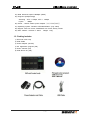
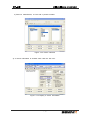
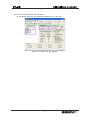
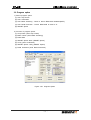
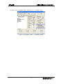
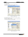
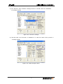
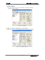
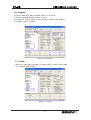
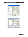
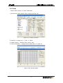
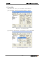
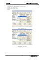
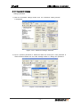
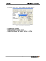
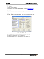
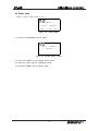
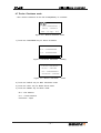
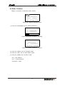
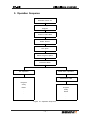
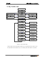
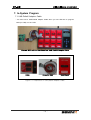
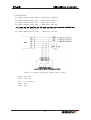
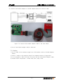
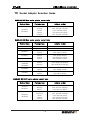
Revision 1.4
User's Manual
GW-uni2
Universal gang programmer
WWW.SEMINIX.COM
Important Notice
The information in this publication has been carefully checked and believed to be entirely
accurate at the time of publication. SEMINIX assumes no responsibility, however, for possible
errors or omissions, or for any consequences resulting from the use of the information contained
herein. SEMINIX, continues to improve products and upgrade specification, and firmware at any
time without notice.
SEMINIX reserves the right to make changes in its products or product specifications with the
intent to improve function or design at any time and without notice and is not required to update
this documentation to reflect such changes.
SEMINIX makes no warranty, representation, or guarantee regarding the suitability of its
products for any particular purpose, nor does SEMINIX assume any reliability arising out of the
application or use of any product or circuit and specifically disclaims any and all liability,
including without limitation any consequential or incidental damages.
© 2011 SEMINIX Co., Ltd.
This publication contains proprietary information, which is protected by copyrights. All rights are
reserved. No part of this publication may be photocopied, reproduced, transmitted in any form or
translated to another language by means, electric or mechanical, by photocopying, recording, or
otherwise, without the prior written consent of SEMINIX Co., Ltd.
Seminix Co., Ltd.
204-ho, 2ndFl. Leader's Building, #342-1
Yatap-dong, Bundang-Gu, Seongnam-si, Kyeonggi-do
Korea (463-828)
Web Address : http://www.seminix.com
E-mail: [email protected]
Tel+82-31-703-7891 Fax : +82-31-702-7869
Table of Contents
1. Overview
1.1 Features and Specifications ------------------------------------------------------------- 1
1.2 Packing Includes ---------------------------------------------------------------------------- 2
2. Setup
2.1 Host system requirement ---------------------------------------------------------------- 3
2.2 To install PC application program------------------------------------------------------ 3
2.3 To install USB driver ---------------------------------------------------------------------- 3
2.4 GW-uni2 Configuration -------------------------------------------------------------------- 3
3. PC Application Program
3.1 PC application program ------------------------------------------------------------------- 4
3.2 Hardware setup ------------------------------------------------------------------------------ 4
3.3 USB connection ----------------------------------------------------------------------------- 5
3.4 Device selection ----------------------------------------------------------------------------- 6
3.5 File open -------------------------------------------------------------------------------------- 8
3.6 Program option ------------------------------------------------------------------------------ 10
3.7 System Power(VDD), Program Power(VPP) --------------------------------------- 12
3.8 Program count ------------------------------------------------------------------------------- 13
3.9 Data download ------------------------------------------------------------------------------- 15
3.10 Program -------------------------------------------------------------------------------------- 16
3.11 Verify ------------------------------------------------------------------------------------------ 16
3.12 Chip erase ----------------------------------------------------------------------------------- 17
3.13 Blank check -------------------------------------------------------------------------------- 17
3.14 Device checksum ------------------------------------------------------------------------- 18
3.15 Buffer checksum -------------------------------------------------------------------------- 18
3.16 Dump ------------------------------------------------------------------------------------------ 19
3.17 Read Buffer --------------------------------------------------------------------------------- 20
3.18 Key Lock ------------------------------------------------------------------------------------- 21
3.19 Password Change ------------------------------------------------------------------------- 24
3.20 Socket state -------------------------------------------------------------------------------- 26
3.21 State window ------------------------------------------------------------------------------- 27
3.22 GW-uni2 Setting window --------------------------------------------------------------- 27
3.23 Upgrade -------------------------------------------------------------------------------------- 28
4. Stand-alone mode
4.1 System on and initialization ------------------------------------------------------------- 29
4.2 LCD display information ------------------------------------------------------------------ 29
4.3 Program mode ------------------------------------------------------------------------------- 30
4.4 Verification mode ---------------------------------------------------------------------------- 31
4.5 Erase mode ----------------------------------------------------------------------------------- 32
4.6 Blank check mode -------------------------------------------------------------------------- 33
4.7 Device checksum mode ------------------------------------------------------------------ 34
4.8 Buffer checksum mode ------------------------------------------------------------------- 35
4.9 Menu mode ----------------------------------------------------------------------------------- 36
4.10 Device setting ------------------------------------------------------------------------------ 37
4.11 Program option ----------------------------------------------------------------------------- 37
4.12 Read Device -------------------------------------------------------------------------------- 38
4.13 Program count ----------------------------------------------------------------------------- 39
4.14 Beep sound --------------------------------------------------------------------------------- 39
4.15 Information ----------------------------------------------------------------------------------- 39
4.16 Return ----------------------------------------------------------------------------------------- 39
4.17 Result ----------------------------------------------------------------------------------------- 40
4.18 Socket LED --------------------------------------------------------------------------------- 40
4.19 Socket Life Time -------------------------------------------------------------------------- 41
5. Operation Sequence----------------------------------------------------------------------- 42
6. Key Function Map ------------------------------------------------------------------------ 43
7. On-Board Program ----------------------------------------------------------------------- 44
8. Electrical Characteristics -------------------------------------------------------------- 47
9. Special Notice ------------------------------------------------------------------------------- 47
10. Adapter Socket Table ---------------------------------------------------------------- 48
GW-uni2
Universal gang programmer
1. Overview
GW-uni2 is the gang programmer for all SAMSUNG MCU and Fujitsu MCU with
standard serial writing. The Gang programmer consists of a master unit (GW-uni2) which
connects to various programming adapter sockets for programming all devices with a
different package.
This gang programmer can program 8 devices with very fast programming speed once.
It is good for mass production. A data is saved in GW-uni2 memory by PC so it works
without PC (Stand-alone mode). User can easily set a device information by a device
part number selection.
1.1 Features and Specifications
1) Support all SAMSUNG MCUs and Fujitsu MCUs with Standard Serial Writing.
2) Internal Memory: 100Mbyte
3) GW-uni2 setup and initialize with PC application program.
4) Stand-alone operation mode without PC.
(GW-uni2 should be setup by PC application program for the stand-alone mode in advance)
5) Program maximum 8 devices once.
6) Display a current state and a working state by LCD
7) Device selection can be set by a device part number.
8) Program : Data programming to a device.
- Other functions can be worked with program option
9) Program Option
- Auto Chip Erase : Erase before program.
- Auto Verification : Verify after program
- Read Protection : A device ROM data can't be read
- SMART Option
10) Erase : Erase a device ROM data.
11) Verify : Compare a butter memory data to a device data
12) Blank check: Check a device ROM data initialized (0xFF)
13) Device Checksum : Display a checksum of a device in the first socket.
14) Buffer Checksum : Display a checksum of GW-uni2 buffer memory data.
15) Dump : Display a device ROM data or a buffer memory data.
16) Read buffer :
Save a buffer memory data as a PC file.(Intel hex format).
17) Read device : Save a device ROM data in buffer memory.
18) Program counter : Display the number of programed device.
19) Key Lock : Restrict functions in stand-alone mode.
20) Password Change : Change a password
21) GW-uni2 setting information: Display GW-uni2 setting information
22) Socket State : Display each socket state
23) User can use the latest software with a simple upgrade.
- 1 -
GW-uni2
Universal gang programmer
24) Data download speed: 860Kbps (MAX)
25) Program speed(average)
Samsung : OTP = 2KBps, MTP = 10KBps
Fujitsu
:
4KBps
26) Power : 19VDC 500mA power adapter (110/220VAC[60HZ])
27) Operating system: Windows NT/2000/XP/Win7 (only 32bit)
28) Support Intel hex format, SAMSUNG hex format, Binary format.
29) Size: 350mm x 220mm x 35mm
Weight: 1.4kg
1.2 Packing Includes
1) GW-uni2 main body
2) USB Cable
3) Power adapter (19VDC)
4) PC Application program (CD)
5) User's manual (CD)
6) USB Driver file (CD)
- 2 -
GW-uni2
Universal gang programmer
2. Setup
2.1 Host system requirement
1) Over IBM Pentium PC.
2) Window 2000/NT/XP/7 32bit-OS
3) CD-ROM, USB port
4) Operating System with 20MB of free Hard disk space
5) Over RAM 64MB
2.2 To install PC application program
1) Insert the installation CD into CD-ROM drive on your PC or download software at
SEMINIX web site. (www.seminix.com).
2) Execute the setup file in CD.
3) Install PC application program in order according to the instruction.
4) The program is installed at the folder "C:\Program Files\seminix\GW-uni2"
when the installation is finished.
2.3 To install USB driver
1) After restarting a host PC, connect GW-uni2 to USB port of the host PC
Then, the PC displays " Found New hardware Wizard" dialog.
2) Select ' C:\Program Files\seminix\GW-uni2\drives and finish the setup.
2.4 GW-uni2 Configuration
.
➀ Socket connection port
➁ LCD panel
➂ Touch Key
➃ Power switch
➄ Adapter connection port
➅ USB connection port
Figure 2.4 GW-uni2 configuration (Front/Side)
- 3 -
GW-uni2
Universal gang programmer
3. PC Application Program
3.1 PC application program
1) Selection a device for program and send information of device to GW-uni2.
2) Download a data for program to GW-uni2 buffer memory.
3) Set Program Option.
4) Program count can be cleared.
5) Execute Erase, Write, Verify, Blank Check, Device Checksum, Buffer Checksum,
Dump and Read Buffer
7) GW-uni2 software upgrade.
3.2 Hardware setup
1) Connect a power adapter to GW-uni2 and turn on the power
2) Connect GW-uni2 to PC by USB cable.
3) Put a adapter socket in GW-uni2.
4) Put a device chip in a socket adapter.
Figure 3.2 GW-uni2 Hardware setup
- 4 -
GW-uni2
Universal gang programmer
3.3 USB Connection
1) Execute the application program and click the USB connection icon.
Figure 3.3.1 USB Connection
2) “** GW-uni2 is connected **" message and information of 'GW-uni2 setting', 'Program
count' and 'Program Option setting' are displayed when GW-uni2 is connected
by USB.
Figure 3.3.2 Finish USB connection
* Try from 1) again when USB connection is failed.
- 5 -
GW-uni2
Universal gang programmer
3.4 Device selection
1) Click the 'Device' icon.
Figure 3.4.1 Device selection
2) 'Select Device' Window is displayed.
Figure 3.4.2 'Select Device' Window
- 6 -
GW-uni2
Universal gang programmer
3) Select a manufacturer, a Core and a product number.
Figure 3.4.3 Device selection
4) A device information is showed when click the 'OK' icon.
Figure 3.4.4 Display a device information
- 7 -
GW-uni2
Universal gang programmer
3.5. File open
1) Click the file open icon.
Figure 3.5.1 File open
2) Select a file(*.hex or *.bin).
Figure 3.5.2 File selection.
- 8 -
GW-uni2
Universal gang programmer
3) Check the end address and checksum.
* It can take a little time for checksum depending on a file size.
Figure 3.5.3 Finish the file selection
- 9 -
GW-uni2
Universal gang programmer
3.6 Program option
1) Select program option.
(1) Auto Chip Erase
(2) Auto Verification
(3) Auto Blank Checking : Check a device ROM data initialized(0xFF)
(4) Auto Read Protection : Device ROM data is read as '0'
(6) SMART Option
2) Process of program option.
(1) Chip Erase (Auto Chip Erase)
(2) Blank Check (Auto Blank Checking)
(3) Data Write
(4) SMART Option Write (SMART Option)
(5) Verify (Auto Verification)
(6) SMART Option Verify (SMART Option)
(7) Read Protection (Auto Read Protection)
Figure 3.6.1 Program Option
- 10 -
GW-uni2
Universal gang programmer
3) There is an unavailable option depending on a selected device.
Figure 3.6.2 Program Option - unavailable Option
- 11 -
GW-uni2
Universal gang programmer
3.7 System Power(VDD), Program Power(VPP)
1) VDD : System power setting - User can set 3.3V or 5.0V.
Figure 3.7.1 VDD setting
2)
VPP : Program power setting - User can set VPP from 3.3V to 12.5V in
the unit of 0.1V
Figure 3.7.2 VPP setting
- 12 -
GW-uni2
Universal gang programmer
3.8 Program count
1) Success Num : Display the number of program success
2) Fail Num : Display the number of program fail
Figure 3.8.1 Program Count
3) The initialization window of 'Success Num' and 'Fail Num' is showed
after click the 'Clear Count' button.
4) The count is initialized when user puts a password on 'Password' blank
in 'Clear count' and clicks 'Clear Count' button.
Figure 3.8.2 Clear Count
- 13 -
GW-uni2
Universal gang programmer
5) The 'Success: Count Cleared!' message window is showed when the initialization
is normally finished.
Figure 3.8.3 Success message
6) 'Success Num' and 'Fail Num' is initialized to ‘0’ after the 'Clear Count' process is
normally finished.
Figure 3.8.4 Clear Program Count
- 14 -
GW-uni2
Universal gang programmer
3.9 Data download
1) Save the selected file data, device information and program options etc.
to GW-uni2 internal memory.
Figure 3.9.1 Download
2) Display the message "Download Success!" after download
3) Display information on 'GW-uni2 Setting Information’ window after download.
Figure 3.9.2 Download Success
- 15 -
GW-uni2
Universal gang programmer
3.10 Program
1) Write a data from GW-uni2 buffer memory to a device.
2) Execute selected program options in order.
3) Display the program result of each socket in ‘Socket state’ windows.
4) Program count is renewed.
Figure 3.10 Program
3.11 Verify
: Display the result after comparing a written data of a device and a data
of a GW-uni2 buffer memory.
Figure 3.11 Verify
- 16 -
GW-uni2
Universal gang programmer
3.12 Chip erase
:
Delete a device ROM data..
Figure 3.12 Erase
3.13 Blank check
: Check a device ROM data initialized(0xFF)
Figure 3.13 Blank Check
- 17 -
GW-uni2
Universal gang programmer
3.14 Device checksum
:
Display a device checksum in the #1(Master) socket of 8 sockets.
Figure 3.14 Device Checksum
3.15 Buffer checksum
: Display a checksum of GW-uni2 internal memory data.
Figure 3.15 Buffer Checksum
- 18 -
GW-uni2
Universal gang programmer
3.16 Dump
: Display buffer memory or device ROM data.
1) Execute the Dump window after clicking the dump icon.
Figure 3.16.1 Dump execution
2) Address is changed by '<<' and '>>' button.
3) 'Buffer Memory' : Display buffer memory data.
4) 'Device<Socket#1>' : Display device ROM data in a socket #1.
Figure 3.16.2 Dump window
- 19 -
GW-uni2
Universal gang programmer
3.17 Read Buffer
: Read data in buffer memory and save it as an intel hex file to PC
1) Click 'Read Buffer' button and the password window is displayed.
Figure 3.17.1 Read Buffer execution
2) Input password and click 'Check' button and start to execute Read Buffer.
Figure 3.17.2 Input password
- 20 -
GW-uni2
Universal gang programmer
3) File address is displayed after 'Read Buffer' is completed
Figure 3.17.3 Complete 'Read Buffer'
3.18 Key Lock
: If the 'Key Lock Selected', the following function will be protected
- PC Application Program
: 'Device Selection', 'Download', 'Program Option', 'Dump' function
- Stand-alone mode
: 'Device Setting', 'Program Option' and 'Read Device' function
1) Click the 'Key Lock' check box and
'Key Lock' setting window is displayed.
Figure 3.18.1 Key Lock execution
- 21 -
GW-uni2
Universal gang programmer
2) Input password and click 'Lock' or 'Unlock' button
3) 'Lock'
: Set the key lock
4) 'Unlock': Set the key unlock
5) 'Exit'
Figure 3.18.2 Key Lock
Figure 3.18.3 Key Unlock
- 22 -
GW-uni2
Universal gang programmer
Figure 3.18.4 Key lock mode - Device Selection Error
* This function helps to avoid an operator's mistake in the mass production line.
* You must set Password before use this function.( refer to 3.19 Password Change )
- 23 -
GW-uni2
Universal gang programmer
3.19 Password Change
: Change password
1) Click the 'Password Change' button and
the 'Password' setting window
is displayed
Figure 3.19.1 'Password Change' execution
2) Input a previous password in 'Password' blank box and input a new password in
'New Password' blank box and click 'Change' button to change the password
Figure 3.19.2 Password Change
- 24 -
GW-uni2
Universal gang programmer
3) A message window about a result is displayed after changing password.
Figure 3.19.3 Finish Password Change
- A password is not set at first
- Password can be set to maximum 8 words.
- Password is not set when 'New Password' blank box is not filled.
- 25 -
GW-uni2
Universal gang programmer
3.20 Socket state
: Display an operating result on each socket.
Figure 3.20 Display a socket state
3.21 State window
: Display an operating result on the 'Socket State' window.
Figure 3.21 State Window
- 26 -
GW-uni2
Universal gang programmer
3.22 GW-uni2 Setting window
: Display GW-uni2 setting state.
Figure 3.22 GW--uni2 setting window
1) Device : Display a device name.
2) Start Address : Display a program start address.
3) End Address : Dispaly a program end address.
4) Checksum : Display a data checksum which is downloaded.
5) VDD : Display a system voltage.
6) VPP : Display a program voltage.
GW-uni2 works based on GW-uni2 setting information so check whether GW-uni2
setting is changed after changing GW-uni2 setting information. (device information,
Program option, Download etc.)
* The setting value is displayed when GW-uni2 is connected to PC GW-uni2 normally.
- 27 -
GW-uni2
Universal gang programmer
3.23 Upgrade
- Upgrade GW-uni2 software.
- Please check a new firmware file at SEMINIX homepage(www.seminix.com)
periodically
- User can check the version information at 'Help -> About GW-uni2... ' menu
1) Upgrade process
(1) Write "UPGRD" to the 'Start Address' blank and then enter the 'Enter' key.
Figure 3.23 Upgrade Start
(2) The upgrade data is downloaded when user enters 'Enter key'
(3) GW-uni2 is upgraded after finish the download.
(4) Restart GW-uni2 about 20 min later (Power off -> Power On)
- 28 -
GW-uni2
Universal gang programmer
4. Stand-alone mode
4.1 System on and initialization
: To use GW-uni2 with stand-alone mode, user should setup PC application program
and download a data first
Touch keys don't work if the USB cable is connected so please disconnect
USB cable for the stand-alone mode.
1) Set a device with reference to ‘3.4 Device selection’
2) Set a program option with reference to ‘3.6 Program Option’
3) Download a data with reference to ‘3.5 File Open’,‘3.9 Data Download'
4) Disconnect USB cable. (The key is not working when USB cable is connected)
5) The system information is kept until user set it again.
4.2 LCD display information
: There is a program standing mode when user turns on GW-uni2 power
after initialization
Program Option
[
PROGRAM
]
Current Mode
Device : S3F9454
Device Name
Vdd : 5.0 Vpp : 12.5
Device Information
Figure 4.2 LCD display
1) Program Option : Display Program option
(1)
: Auto Chip Erase
(2)
: Auto Verification
(3)
: Auto Blankcheck
(4)
: Auto Read Protection
(5)
: Auto LDC Protection
(6)
: Auto Hard Lock
(7)
: SMART Option
2) Current Mode : Display a current mode.
(1) PROGRAM, VERIFICATION, ERASE, BLANK CHECK, DVC CHECKSUM,
and BUF CHECKSUM
(2) A mode is changed in order when touch 'LEFT' and 'RIGHT' keys.
- 29 -
GW-uni2
Universal gang programmer
3) Device Name
: Display a device name.( Display 'Nothing' when there is not any selected device)
4) Device Information : Display Device setting information..
(1) Vdd : System Power (Voltage)
(2) Vpp : Program Power (Voltage)
(3) E.A : End Address (Hex)
(4) Checksum : Buffer Checksum (Hex)
4.3 Program mode
: Program standing state
[
PROGRAM
]
Device : S3F9454
Vdd : 5.0 Vpp : 12.5
Figure 4.3.1 Program Mode
1) Touch 'PROGRAM' key and execute the program mode.
Device : S3F9454
<
Write
>
25%
Figure 4.3.2 Program Mode - Write to a device
2) Execute a program option together
3) Touch the 'RIGHT' key for 'Verification mode'
4) Touch the 'LEFT' key for 'Buf Checksum mode'
5) Touch the 'MENU' key for 'Menu mode'.
- 30 -
GW-uni2
Universal gang programmer
4.4 Verification mode
[
VERIFICATION
]
Device : S3F9454
Vdd : 5.0 Vpp : 12.5
Figure 4.4.1 Verification Mode
1) Touch the 'PROGRAM' key for verify.
Device : S3F9454
<
Verify SMCU
>
25%
Figure 4.4.2 Verification mode - Verify
2) Touch the 'RIGHT' key for 'Erase mode'.
3) Touch the 'LEFT' key for 'Program mode'.
4) Touch the 'MENU' key for 'Menu mode'.
- 31 -
GW-uni2
Universal gang programmer
4.5 Erase mode
: Make a device ROM initialize (0xff)
[
ERASE
]
Device : S3F9454
Vdd : 5.0 Vpp : 12.5
Figure 4.5.1 Erase Mode
1) Touch the 'PROGRAM' key for erase.
Device : S3F9454
<
ERASE
>
Figure 4.5.2 Erase Mode - Erase
2) Touch the 'RIGHT' key for 'Blank Check mode'.
3) Touch the 'LEFT' key for 'Verification mode'.
4) Touch the 'MENU' key for 'Menu mode'.
- 32 -
GW-uni2
Universal gang programmer
4.6 Blank Check mode
: Check a device ROM data initialized(0xff)
[
BLANK CHECK
]
Device : S3F9454
Vdd : 5.0 Vpp : 12.5
Figure 4.6.1 Blank check mode
1) Touch the 'PROGRAM' key for 'Blank Check'.
Device : S3F9454
<
Blank Check
>
25%
Figure 4.6.2 Blank check mode - Blank check
2) Touch the 'RIGHT' key for 'DVC Checksum mode'.
3) Touch the 'LEFT' key for 'Erase mode'.
4) Touch the 'MENU' key for 'Menu mode'.
- 33 -
GW-uni2
Universal gang programmer
4.7 Device Checksum mode
: Get a device checksum in the first socket(Master) of 8 sockets
[
DVC CHECKSUM
]
Device : S3F9454
Vdd : 5.0 Vpp : 12.5
Figure 4.7.1 Device checksum mode
1) Touch the 'PROGRAM' key for device checksum.
<
Checksum
>
E.A : 0xXXXXXXXX
C.A : 0xXXXXXXXX
25%
Figure 4.7.2 Device Checksum - Loading
< Device Checksum >
Device : S3F9454
E.A : 0xXXXXXXXX
CheckSum : 0xXXXX
Figure 4.7.3 Device Checksum
2) Touch the 'RIGHT' key for 'BUF Checksum mode'.
3) Touch the 'LEFT' key for 'Blank Check mode'.
4) Touch the 'MENU' key for 'Menu mode'.
* E.A : End Address
* C.A : Current Address
* Checksum : 2byte
- 34 -
- Done
GW-uni2
Universal gang programmer
4.8 Buffer Checksum
: Display a checksum of GW-uni2 buffer memory.
[
DVC CHECKSUM
]
Device : S3F9454
Vdd : 5.0 Vpp : 12.5
Figure 4.8.1 Device checksum mode
1) Touch the 'PROGRAM' key for 'Buffer Checksum'.
Buffer Checksum
E.A : 0xXXXXXXXX
C.A : 0xXXXXXXXX
25%
Figure 4.8.2 Buffer Checksum - Loading
Buffer Checksum
Buffer Memory
E.A : 0xXXXXXXXX
CheckSum : 0xXXXX
Figure 4.8.3 Buffer Checksum
2) Touch the 'RIGHT' key for 'Program mode'..
3) Touch the 'LEFT' key for 'DVC Check mode'.
4) Touch the 'MENU' key for 'Menu mode'.
* E.A : End Address
* C.A : Current Address
* Checksum : 2byte
- 35 -
- Done
GW-uni2
Universal gang programmer
4.9 Menu mode
: Touch the key for Menu mode in 'Program Mode', 'Verification Mode' and
'Erase Mode'
Menu
Device Checksum
Buffer Checksum
Program Count
Figure 4.9.1 Menu Mode
1) Menu
(1) Device Setting : Set a device value by part no.
(2) Program Option : Select a program option.
(3) Read Device : Read a device ROM data and save it to a buffer memory.
(4) Program Count : Display the programed device number.
(5) Beep Sound : On and off the beep sound.
(6) Information : Display GW-uni2 information.
(7) Return : Return to previous mode.
2) Display the chosen menu with an inverted color.
3) Menu can be changed by 'UP' and 'DOWN' key.
4) Touch the 'MENU' key to select a chosen menu.
5) Touch the 'PROGRAM' key for a previous mode.
- 36 -
GW-uni2
Universal gang programmer
4.10 Device Setting
: Change system setting value depending on a chosen device.
Device Name
S3F80JB
S3P80K5
S3P80K9
Figure 4.10 Device Setting
1) Display a chosen device with an inverted color
2) A device can be changed by 'UP' and 'DOWN' key.
3) Touch the 'MENU' key to select a chosen menu.
4) Touch the 'PROGRAM' key for a previous mode.
*This device setting can't used if there is the 'Key lock' setting.
4.11 Program Option
: Change a program option.
Device Name
Verification
Blank Check
ReadProtection
Figure 4.11 Program Option
1) Display an icon when an option is chosen.
2) An option can be changed by 'UP' and 'DOWN' key.
3) Touch the 'MENU' key to select a chosen option.
4) Touch the 'PROGRAM' key for a previous mode.
5) Back to a menu mode when 'Return' is selected.
*This program option can't be used if there is the 'Key lock' setting.
- 37 -
GW-uni2
Universal gang programmer
4.12 Read Device
: Read a device ROM data in the socket #1 and save it to GW-uni2 buffer memory.
1) Display a device setting menu when 'Read Device' is selected.
Device Name
S3F80JB
S3F80K5
S3F80K9
Figure 4.12.1 Device selection
2) Display a confirmation window when a device is selected.
Read Device
Device Name
Continue?
[ NO ]
YES
Figure 4.12.2 Read Device confirmation
3) Back to a menu mode when 'NO' is selected.
4) Execute 'Read Device' when 'YES' is selected.
< Read Device >
E.A : 0xXXXXXXXX
C.A : 0xXXXXXXXX
25%
Figure 4.12.3 Read Device - Loading
5) Back to a previous mode when 'Read Device' is finished.
*This Read Device can't be used if there is the 'Key lock' setting.
- 38 -
GW-uni2
Universal gang programmer
4.13 Program Count
(1) Success : The number of program success.
(2) Fail
: The number of program fail.
Program Count
Success
:
000000
Fail
:
000000
Figure 4.13 Program Count
4.14 Beep Sound
: On and off beef sound.
Beep Sound?
[ ON ]
OFF
Figure 4.14 Beep Sound
4.15 Information
(1) Display a hardware version.
(2) Display a software version.
(3) Display a buffer memory size.
INFORMATION
H / W
:
Ver 2.0
S / W
:
Ver 1.0
Memory
:
100 MB
Figure 4.15 Information
4.16 Return
: Back to the previous mode (Program Mode, Verification Mode, Erase Mode)
- 39 -
GW-uni2
Universal gang programmer
4.17 Result
1) Display an operating result of each socket.
2) Display "G" with programming success.
Display "F" with programming fail.
Display "I" with Socket Mismatch fail. (Device setting - Socket)
Display "E" with End of Socket-Life-Time.
[
RESULT
]
G G G G
G G G G
Figure 4.17 Display LCD Result
4.18 Socket LED
State
LED RED
LED GREEN
Stand By
OFF
ON
Execute Function
X
X
Success
OFF
OFF
Fail
ON
OFF
Result
Table 4.18 Socket LED Description
- 40 -
GW-uni2
Universal gang programmer
4.19 Socket Life Time
The socket adapter consists of several mechanical parts so that it is consumption
goods, whose life time is limited. GW-uni2 will display the warning message on the
LCD of GW-uni2 when the programming counts of the socket adapter reaches the
life time (counts) of its socket adapter.
[
WARNIGN!
]
Socket LifeTime
#1
#2
#4
Socket No.
#6
#8
Socket No.
4.19 Socket Life Time
After the warning message is displayed, GW-uni2 will program the devices
continuously until 10% over counts than the life time count of socket adapter.
So GW-uni2 will not program the devices when the programming count is over than
10% of the life time (count) of the socket adapters because the programming
reliability could not be guaranteed.
Please change the used socket adapters into new ones in case of that, and then
program the devices continuously.
- 41 -
GW-uni2
Universal gang programmer
5. Operation Sequence
GW-uni2 Power On
Execute PC Application
Program
Connect USB cable
Select Device
File Open
Select Program Option
Download Data
PC Operation
Stand-alone Operation
Disconnect USB
Program
Verify
Erase
Program
.
Verify
.
Erase
.
.
.
.
Figure 5.1 Operation Sequence
- 42 -
GW-uni2
Universal gang programmer
6. Key Function map
GW-uni2 Power ON
Initial System
BUF Checksum
'RIGHT'
'LEFT'
Program
'RIGHT'
'LEFT'
'LEFT' 'RIGHT'
DVC Checksum
Verification
'LEFT' 'RIGHT'
'RIGHT'
'LEFT'
Blank Check
'RIGHT'
'LEFT'
Erase
'MENU'
Menu
'UP'
Device Setting
'MENU'
Execute
Device Checksum
'MENU'
Execute
Buffer Checksum
'MENU'
Execute
Read Device
'MENU'
Display
Program Count
'MENU'
Beep Sound
On/Off
'MENU'
Display
Information
'MENU'
Return to
Last Mode
'UP' 'DOWN'
Program Option
'UP' 'DOWN'
Read Device
'UP' 'DOWN'
Program Count
'UP' 'DOWN'
Beep Sound
'UP' 'DOWN'
Information
'UP' 'DOWN'
Return
'DOWN'
Figure 6.1 Key Function Map
* Please make sure that USB cable should not be connected when user want to use
the stand-alone mode because 'Key' is not working when USB cable is connected.
- 43 -
GW-uni2
Universal gang programmer
7. In-System Program
7.1 UAS-Pellet2 Adapter Cable
: You must use a UAS-Pellet2 Adapter Cable when you use GW-uni2 to program
MCU(or COB) on the PCB.
Connect GW-uni2 to User board via UAS-Pellet2 Adapter Cable
20CB6
Connection Cable
Socket Board
Figure 7.1 Component of UAS-pellet2 Adapter Cable
- 44 -
GW-uni2
Universal gang programmer
7.2 Connection
(1) 20CB6-Adapter Board 'GND' - Target-MCU 'GND(Vss)'
(2) 20CB6-Adapter Board 'VDD' - Target-MCU 'Vdd(Vcc)'
(3) 20CB6-Adapter Board 'RST' - Target-MCU 'Reset'
(4) 20CB6-Adapter Board 'VPP' - Target-MCU 'Vpp(Test)'
* if 'Reset pin' and 'Vpp(Test) pin' are same, you have only to connect 'Vpp(Test) pin'.
(5) 20CB6-Adapter Board 'SCLK' - Target-MCU 'SCLK'
(6) 20CB6-Adapter Board 'SDAT' - Target-MCU 'SDATA'
20CB6-Adapter board
( component of UAS-Pellet2 Adapter Cable )
Figure 7.2 Connect UAS-Pellet2 Adapter Cable to MCU
Rsdat : 4.7K ohm
Rclk
: 4.7K ohm
Rrst
: 1K~4.7K ohm
Cvpp : 10nF
Cvdd : 10nF
- 45 -
GW-uni2
Universal gang programmer
2) Connect UAS-Pellet2 Adapter to 20CB6 Adapter-Board via connect cable.
Figure 7.3 Connect UAS-Pellet2 Adapter cable to the User Board
3) Put a UAS-Pellet2 adapter cable in GW-uni2.
7.3 Caution
1) 2m of cable is the maximum length from UAS-Pellet2 socket to 20CB6-Adapter
Board
2) 20cm of cable is the maximum length from Adapter-Board to Target-MCU.
3) if you program to MCU on board, you must use the UAS-Pellet2 Adapter Cable.
4) Please check components - Rsdat, Rclk, Rrst, Cvpp, Cvdd.
- 46 -
GW-uni2
Universal gang programmer
8. Electrical Characteristics
Parameter
Conditions
Min
Typ
Max
Stand By
-
-130
-150
Operating
-
-
-300
VDD
VPP 3.3 ~ 12.5
3.3
5.0
V
VPP
VDD 3.3 or 5.0
3.3
12.5
V
Current Consumption
VDD = 3.3V
Idd
VDD = 5.0V
VDD = 3.3V
Ipp
VDD = 5.0V
Unit
mA
VPP=3.3V
-
-
500
mA
VPP=12.5V
-
-
500
mA
VPP=5.0V
-
-
500
mA
VPP=12.5V
-
-
500
mA
VPP=3.3V
-
-
25
mA
VPP=12.5V
-
-
25
mA
VPP=5.0V
-
-
25
mA
VPP=12.5V
-
-
25
mA
9. Special Notice
1) Please make sure to check device information, End address, Vdd, Vpp,
buffer check sum before programming.
2) Please check device checksum regularly for normal programming
3) Please check Vdd and Vpp regularly
4) Please contact SEMINIX when there is a problem of device programming
5) GW-uni2 is the socket programmer only so SEMINIX can't take the responsibility
for all accidents after user's artificial manipulation without SEMINIX socket
6) SEMINIX doesn't take the responsibility of GW-uni2 from user's careless mistake.
- 47 -
GW-uni2
10.
Universal gang programmer
Socket Adapter Selection Guide
SAMSUNG S3F9xxx series adapter socket table
Device Name
Package type
Adapter socket
S3F94C4
S3F94C8
16SOP
16TSOP
20DIP
20SOP
20SSOP
UAS-94C4/8-16SOP
UAS-94C4/8-16TSOP
UAS-94C4/8-20DIP
UAS-94C4/8-20SOP
UAS-94C4/8-20SSOP
SAMSUNG S3F8xxx series adapter socket table
Device Name
Package type
Adapter socket
S3F80Q5
24ELP
UAS-80Q5-24ELP
S3F80QB
44ELP
UAS-80QB-44ELP
S3F80P5
24SOP
24SDIP
UAS-80P5-24SOP
UAS-80P5-24SDIP
28SOP
32SOP
44QFP
UAS-80P9-28SOP
UAS-80P9/B-32SOP
UAS-80P9/B-44QFP
S3F8285
S3F8289
S3F828B
80QFP
80TQFP
UAS-8285/9/B-80QFP
UAS-8285/9/B-80TQFP
S3F84B8
20DIP
20SOP
UAS-84B8-20DIP
UAS-84B8-20SOP
S3F84I9
42SDIP
44QFP
UAS-84I9-42DIP
UAS-84I9-44QFP
S3F80P9
S3F80PB
SAMSUNG S3F8XXX series adapter socket table
Device Name
Package type
Adapter socket
S3F8S15
S3F8S19
48QFP
48TQFP
48ELP
UAS-8S15/9-48QFP
UAS-8S15/9-48TQFP
UAS-8S15/9-48ELP
S3F8S24
S3F8S28
24SOP
24TSSOP
20DIP
20SOP
20SSOP
UAS-8S24/8-24SOP
UAS-8S24/8-24TSOP
UAS-8S24/8-20DIP
UAS-8S24/8-20SOP
UAS-8S24/8-20SSOP
- 48 -
GW-uni2
Universal gang programmer
SAMSUNG S3F8XXX series adapter socket table
Device Name
Package type
Adapter socket
S3F8S34
S3F8S35
S3F8S38
S3F8S39
32SOP
32SDIP
32ELP
UAS-8S34/5/8/9-32SOP
UAS-8S34/5/8/9-32SDIP
UAS-8S34/5/8/9-32ELP
S3F8S45
44QFP
UAS-8S45-44QFP
S3F8S5A
44QFP
UAS-8S5A-44QFP
S3F8S6B
64QFP
64SDIP
UAS-8S6B-64QFP
UAS-8S6B-64SDIP
S3F8S7B
80QFP
80TQFP
UAS-8S7B-80QFP
UAS-8S7B-80TQFP
S3F8S8B
100QFP
100TQFP
UAS-8S8B-100QFP
UAS-8S8B-100TQFP
SAMSUNG On-board Chip/COB type adapter cable
Device Name
Package type
Adapter socket
In-System
Programing
Samsung
Standard
UAS-Pellet2
COB
(Chip On Board)
Pellet(Die form)
UAS-Pellet2
SAMSUNG CalmRISC16 (S3FCXXX) series adapter socket table
Device Name
Package type
Adapter socket
S3FC40D
100QFP
100TQFP
128QFP
UAS-C40D-100QFP
UAS-C40D-100TQFP
UAS-C40D-128QFP
SAMSUNG ARM7 series adapter socket table
Device Name
Package type
Adapter socket
S3F4A0K
144LQFP
UAS-4A0K-144LQFP
S3F4A1H
100TQFP
UAS-FA1H-100TQFP
S3F4A2F
80TQFP
UAS-4A2F-80TQFP
S3F401F
100QFP
UAS-401F-100QFP
- 49 -