1
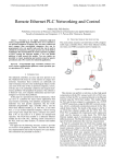
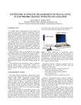
17th Telecommunications forum TELFOR 2009
Serbia, Belgrade, November 24-26, 2009.
VIRTEX II Timing-Simulation vs Reality
Silvana POPESCU, Aurel GONTEAN
High-speed SelectMAP FPGA configuration from
Platform
Flash
In-System
Programmable
Configuration PROM;
Support for ―Golden‖ and ―User‖ FPGA configuration
bitstreams;
On-board 10/100 Ethernet PHY device;
Silicon Serial Number for unique board identification;
RS-232 DB9 serial port;
Two PS-2 serial ports;
Four LEDs connected to Virtex-II Pro I/O pins;
Four switches connected to Virtex-II Pro I/O pins;
Five push buttons connected to Virtex-II Pro I/O pins;
Six expansion connectors joined to 80 Virtex-II Pro I/O
pins with over-voltage protection;
High-speed expansion connector joined to 40 Virtex-II
Pro I/O pins that can be used differentially or single
ended;
AC-97 audio CODEC with audio amplifier and
speaker/headphone output and line level output;
Microphone and line level audio input;
On-board XSGA output, up to 1200 x 1600 at 70 Hz
refresh;
Abstract — The goal of this paper is understanding the
performance capability of a modern FPGA in a post-layout
simulator using a typical design. For this, an eight-phase
generator was used as a test circuit and the delays between
the outputs have been evaluated and corrected.
Keywords — FPGA, rise time, simulation, VHDL.
I. INTRODUCTION
(Field-Programmable Gate Array) is an
manufacturing. FPGAs contain programmable logic
components called logic blocks and a hierarchy of
reconfigurable interconnects that allows the blocks to be
wired together. To define its behavior, the FPGA is
programmed generally using a hardware description
language (HDL). The most common language is VHDL
(VHSIC – Very High Speed Integrated Circuits Hardware
Description Language).
VHDL is used for two different goals: simulation of
electronic designs and synthesis of such designs. Synthesis
is a process where a VHDL is compiled and mapped into
an implementation technology such as a FPGA. Also,
VHDL allows the description of a concurrent system
unlike some programs in which the code run
sequentially[1].
A
FPGA
II. HARDWARE AND SOFTWARE RESOURCES
A. Virtex II Board
The Virtex-II Pro Development System provides an
advanced hardware platform that consists of a high
performance Virtex-II Pro Platform FPGA surrounded by
a comprehensive collection of peripherial components that
can be used to create a complex system and to demonstrate
the capabilities of the Virtex-II Pro Platform FPGA.
Based on the Virtex-II Pro FPGA, the board can
function as a digital design trainer, a microprocessor
development system or a host for embedded processor
cores and complex digital systems.
Features of Virtex-II board:
Virtex-II Pro FPGA with PowerPC 405 cores;
Up to 2 GB of Double Data Rate (DDR) SDRAM;
System AC controller and Type II CompactFlash
connector for FPGA configuration and data storage;
Embedded Platform Cable USB configuration port;
Fig. 1. Virtex-II Board
Three Serial ATA ports, two Host ports and one Target
port;
Off-board expansion MGT link, with user-supplied
clock;
100 MHz system clock, 75 MHz SATA clock;
Provision for user-supplied clock;
S. P. - PhD student, Faculty of Electronics and Telecommunication,
―Politehnica‖ University of Timisoara, Romania (phone: +4-0724214627;
e-mail: [email protected]).
A. G. – Applied Electronics Departament, Faculty of Electronics and
Telecommunications , ―Politehnica‖ University of Timisoara, Romania;
(phone: +4-0745119858; e-mail: [email protected]).
755
entity 8phase is
port( clk:in std_logic;
reset, start. restart: in std_logic;
OUT: out std_logic_vector(1 to 8));
End 8phase;
On-board power supplies;
Power-on reset circuitry;
PowerPC 405 reset circuitry[2].
B. Virtex-II Pro Family FPGA
The Virtex-II Pro/Virtex-II Pro X family is the first
FPGA family to incorporate both serial transceiver
technology and a hard processor core within a generalpurpose FPGA device. This is significant for new highbandwidth embedded processing applications such as
packet processing, where both high device I/O bandwidth
and high performance processor cores are needed together.
The Virtex-II Pro/Virtex-II Pro X family marks the first
paradigm change from programmable logic to
programmable systems, with profound implications for
leading-edge system architectures in networking
applications, deeply embedded systems, and digital signal
processing systems. It allows custom user-defined system
architectures to be synthesized, next-generation
connectivity standards to be seamlessly bridged, and
complex hardware and software systems to be codeveloped rapidly with insystem debug at system speeds.
Together, these capabilities usher in the next
programmable logic revolution[3].
architecture 8phase_arch of 8phase is
signal R_W: std_logic_vector(1 to 8);
signal Aux: std_logic;
begin
process(clk, R_W)
begin
if (clk‘event and clk=‘1‘) then
if (reset=‘1‘) then Aux <= ‗1‘;
R_W <= (‗0‘,‘0‘,‘0‘,‘0‘,‘0‘,‘0‘,‘0‘,‘0‘);
elsif ((R_W=(‗0‘,‘0‘,‘0‘,‘0‘,‘0‘,‘0‘,‘0‘,‘0‘)) or
(restart=‘1‘))
then Aux <= ‗1‘;
R_W <= (‗1‘,‘0‘,‘0‘,‘0‘,‘0‘,‘0‘,‘0‘,‘0‘);
elsif (start=‘1‘) then Aux <= not Aux;
if (Aux=‘0‘) then R_W <= R_W(8)&R_W(1 to 7);
end if;
end if;
end if;
OUT <= not R_W;
end process;
end 8phase_arch;
C. Xilinx Web Pack ISE
ISE WebPACK from Xilinx is a design software for
FPGA design solution for Linux, Windows XP and
Windows Vista. ISE WebPACK is used for FPGA and
CPLD design offering HDL synthesis and simulation,
implementation, device fitting, and JTAG programming.
R_W is an internal active-high signal vector, used for
reading and writing what eventually becomes the circuit‘s
output. This signal is inverted to obtain the required
active-low output signal vector.
Aux is an auxiliary state bit to keep track of the two
states within each phase. The OUT[i] and Aux signals are
all outputs from the flip-flops clocked by the same clock
clk[4].
This design is tested in simulation, first behavioral and
then post-routed.
III. DESIGN IMPLEMENTATION AND TESTING
In order to verify the limits of the ISE Web Pack Suite,
the eight-phase generator has been simulated,
implemented and tested.
A. Eight-phase Waveform Generator
The eight-phase generator is an application of shift
registers in ring counters.
A shift register is a cascade of flip-flops, all sharing the
same clock which have their inputs and outputs connected
together, resulting in a circuit that shifts by one position
the information stored in it at every transition of the clock
input. Ring counters are implemented using shift registers
so that the output of the last register is fed to the input of
the first register.
Figure 3 illustrates a ring counter on 8 bits.
B. Behavioral Simulation
The behavioral simulation is used to test the design
functionality.
The behavioral simulation is illustrated in fig.3.
Signal clk is the clock used in the application of the
eight-phase generator, signals start, restart and reset are the
input signals and the OUT[i] signals are active low-phase
outputs[5].
The signals in the selected aria are zoomed and shown in
fig.4.
As expected, fig.4. demonstrates that the behavioral
simulation does not point out any delays.
C. Post-Route Simulation
Unlike the behavioral simulation, in the post-route
simulation, the delays became noticeable. The
encirclements from fig.5 are the delays introduced by the
post-route simulation. One of these delays is shown in
fig.6, namely the delay between the third and the fourth
signal.
Fig.2. A 8 bits ring counter
The VHDL program of the eight-phase waveform
generator is shown below.
756
Fig.3. Behavioral Simulation
Fig.4. Zoomed Behavioral Simulation
Fig.5. The Post-Route Simulation
Fig.6. Zoomed delayed detail between out[3] and out[4]
757
The delays between every two consecutive signals are
listed in Table 1.
E. Correcting the Measured Rise Time
Rise time refers to the time required for a signal to
change from a specificed low value(10%) to a specified
high value(90%).
The relationship between the rise time and the
bandwidth of a digital oscilloscope is given by:
TABLE 1: DELAYS BETWEEN CONSECUTIVE SIGNALS.
Signals
1_2
2_3
3_4
4_5
5_6
6_7
7_8
8_1
Delays [ps]
238
527
104
376
117
208
106
176
The measured rise time is commonly related to the
oscilloscope rise time and the real rise time using the
formula:
The relationship (2) is useble only if tmeasured ≥ tr [7],[8].
Otherwise, the errors make the correction useless. The
oscilloscope rise time is, form its tehnical manual,
400ps.[6]
D. Experimental Results
Experimental results were acquired with a LeCroy
WaveSurfer Xs Series Oscilloscope, a high performance
digital oscilloscope. In order to obtain results, the eight
signals were routed to the two 40-pin right angle
connectors[6].
The first measurement was with the eight signals routed
to the left expansion connector and the second
measurement was with the signals routed to the right
connector.
Fig.7 illustrates the delay between the third and the fouth
signal. The delay is estimated with the skew function of
the digital oscilloscope. The skew function calculates the
delay between two signals in the following way: time of
clock1 edge minus time of the nearest clock2 edge which
represents exactly the delay between the two signals.
The real rise time is shown in Tabel 3.
TABLE 3: REAL RISE TIME
Delay
Signal
3_4
5_6
Measured
rise time
[ps]
606
438
Oscilloscope
rise time
[ps]
400
400
Real rise
time
[ps]
456
178
IV. CONCLUSION
In managing short times, extra care should be taken. The
oscilloscope‘s bandwidth should be at least five times
higher than the fastest clock rate in the design. Otherwise,
in order to make accurate edge-speed measurements on the
signals, you will need to determine the maximum practical
frequency present in the signal.
REFERENCES
[1]
[2]
[3]
[4]
Fig.7. The delay between the third and the fourth signal.
[5]
[6]
Computing all the delays between every two
consecutive signals, Table 2 illustrates some of the most
effective delays.
[7]
[8]
TABLE 2: DELAYS AT THE TWO 40-PIN CONNECTORS.
Delay
Signal
3_4
5_6
Post-route
simulation
[ps]
104
117
1st 40-pin
connector
[ps]
606
438
2nd 40-pin
connector
[ps]
451
1051
758
S. Popescu, A.Gontean, I.Lie, ―Comparing FPGA behavioral
simulation, post-routed simulation with real-life experiments‖—
Accepted for publication at SIITME2009.
XUP Virtex-II Pro Development System, User Manual, Xilinx,
2009.
Virtex II Pro User Guide Family, Xilinx, 2004
J.Wakerly – Digital Design.Principles and Practices, Third Edition,
2006.
ISE 10.1 Quick Start Tutorial, Xilinx, 2008
LeCroy WaveSurfer, Xs Series Oscilloscope Operator’s Manual,
2008
Relating wideband DSO rise time to bandwidth: Lose the 0.35,
Agilent 55W-18024-2, 2009
Understanding Oscilloscope Bandwidth, Rise Time and Signal
Fidelity, Tektronix, 2002.