1
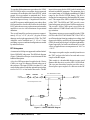
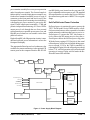
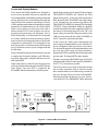
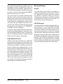
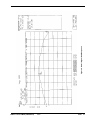
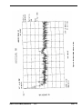
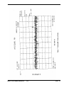
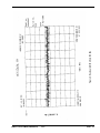
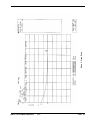
811 Hansen Way
Palo Alto, CA 94303
Phone: (650) 846-3700
Fax: (650) 424-1744
Technical Description
M-Band J Series Compact Medium Power Amplifier
VZM-6993J4
INTRODUCTION
This document provides a detailed technical description of the Communications & Power Industries, Inc. (CPI),
VZM-6993J4 Series M-band Compact Medium Power Amplifier (CMPA), a 250 Watt medium power traveling
wave tube amplifier designed specifically for broadband microwave applications such as EMC and general
purpose testing. The J Series CMPA is compact and lightweight and employs a state-of-the-art wideband
Traveling Wave Tube (TWT). The TWT permits continuous, efficient instantaneous operation across the entire 8.0
to 18.0 GHz frequency. The J Series CMPA also incorporates the use of a microprocessor control system,
thereby simplifying interfacing with remote control and monitor facilities. Both RS 422/485 and IEEE-488
interface ports are included as standard features. Microwave features include a Solid State Intermediate Power
Amplifier (SSIPA), microprocessor controlled RF gain control and soft-fail VSWR protection. The J Series
CMPA also features active power factor correction (0.95 min.) which allows the unit to meet the total harmonic
distortion requirement of EN60555-2. It is also designed to meet EN61010 safety and 89/336/EEC electromagnetic compatibility requirements.
The VZM-6993J4 Series CMPA along with the VZS/C-6963J2 (2.0 – 8.0 GHz) and the VZL-6943J2 (1.0 –
2.5 GHz), cover the full 1.0 – 18.0 GHz in three units. The J Series CMPA family is a member of a comprehensive
line of communication amplifiers including TWT Low Power Amplifiers (LPAs), Medium Power Amplifiers
(MPAs), High Power TWT Amplifiers (HPAs) and High Power Klystron Amplifiers (KPAs) designed specifically
for service in commercial satellite earth stations operating in standard SATCOM frequency bands.
CPI (formerly Varian Electron Device Group) has been active in the design and manufacture of microwave power
amplifiers and related products for more than 30 years. CPI Satcom Division (formerly Varian MEP), was
organized in the mid-1970s to bring together under a single business center the strengths of existing groups
involved with commercial Satcom and Industrial power amplifiers.
Today, CPI Satcom Division has provided thousands of fully integrated satellite uplink power amplifiers in the S,
C, Ku, X, M, DBS and Ka- band frequency ranges to worldwide users and has become the leading supplier of this
class of products.
M-Band J Series CMPA
M-Band J Series CMPA (VZM-6993J4)
04/00
TD-82
1
EQUIPMENT DESCRIPTION
General
The VZM-6993J4 CMPA (Figure 1) is packaged in a
5.25 inch tall slide-mounted drawer suitable for standard 19-inch rack mounting. This enclosed assembly
houses both the RF and power supply sections of the
amplifier. The RF section includes the TWT, solid state
intermediate power amplifier (IPA), optional Input Isolator, input RF Gain control, RF detectors and output
directional couplers for monitoring and protection. The
power supply section includes the power factor correction, power processor, and high voltage regulation
circuitry. It also contains all monitor, control and protection circuits necessary to permit safe, efficient and
reliable operation of the J Series CMPA .
The VZM-6993J4 CMPA is protected from operational damage caused by abnormal AC, DC, RF faults
or insufficient cooling. The amplifier will automatically
recycle itself after a prime power interruption or transient fault condition.
Personnel safety is of utmost importance and is safeguarded by proper grounding and by access interlocks
and shields, which prevent physical entry into the high
voltage sections.
ME TER
S ELE
The front panel of the unit serves as the primary user
interface housing all monitor and control functions including a type N RF connector to sample and measure
output RF power. Opening the small access door on
the front panel allows easy access to configuration DIP
switches that can be set during installation, up/down
buttons that permit setting high and low alarm trip
points (such as Low RF), and a set of detail fault LEDs
to help troubleshoot during operation.
Principal functions are also brought to the four user
interface connectors located on the rear panel for remote monitor and control. Control, fault and monitoring functions are available via: the IEEE-488 interface
designed to interface directly with a computer, an RS422/485 port to be used when the optional CPI remote
control panel is purchased, a separate switching port
for use with switching/power combining subsystems,
and a user interlock port for use when interfacing other
equipment or controls with the J Series CMPA.
Digital attenuation allows for RF drive attenuation adjustment via the remote interface ports thereby enhancing remote monitor and control capabilities.
CT
LOCAL
RF
REM
OU
TPUT
(dB
OU
m)
TPUT
ATTE
(W)
NUA
TOR
REFL
SETT
ECTE
ING
DR
(V)
F(W)
X CUR
RENT
HELI
X VO
(mA)
LTAG
E(kV)
OTE
RF
CIF
HELI
HTD
TX
T RA
N S MI
T
STA
NDB
Y
RE S
SELE
CT
STAN
D BY
ET
TRAN
SM
IT
REC
LO C
AL
RE M
OT E
CI F
YCLE
FAUL D
T
FAUL
T
RF
RF
SET
TIN
SAM
P
G
0
1
Figure 1. J Series CMPA
M-Band J Series CMPA (VZM-6993J4)
04/00
TD-82
2
To expedite field maintenance procedures, the VZM6993J4 CMPA utilizes a modular design approach
consisting of Line Replaceable Units (LRUs), which
permit service personnel to maintain the J Series
CMPA in the field without need of returning the entire
unit to the depot or factory. Comprehensive built-intest (BIT) sequences and diagnostic procedures allow
field personnel to localize the fault to the individual
LRU, make the necessary replacement and return the
amplifier to service with a minimum of operational
downtime.
input is then routed to the SSIPA which includes an
internal variable RF attenuator. The attenuator, has a
user control range of 20 dB plus an additional 15 dB of
range for the soft-fail VSWR feature. The IPA is
designed to be transparent to final amplifier RF parameters. The output of the SSIPA is then fed to the input
of the TWT. The SSIPA and TWT provide a combined subsystem gain of at least 54 dB at rated power.
The overall J Series CMPA gain is specified to be
stable within ±0.25 dB/24 hours with ±10% line voltage variations.
The overall amplifier enclosure measures approximately 19" (w) x 5.25" (h) x 24" (d), plus air duct
adapters, and weighs approximately 70 lbs. The TWT
Amplifier can be installed in a 1:1, 1:2 or 1:3 auto
switching, or power combined configuration as needed
by end user mission.
The primary microwave power amplifier in the VZM6993J4 is the CPI VTM-6294M4 TWT. The TWT is
an efficient design featuring conduction cooling, dual
depressed collectors, and Periodic Permanent Magnet
(PPM) focused helix design. It is lightweight and designed especially for harsh environments in a wide
variety of applications over temperatures of –40°C to
+110 °C.
RF Subsystem
A conservative field-proven approach is utilized in the J
Series CMPA RF subsystem. The RF block diagram
(Figure 2) identifies all major circuit elements for this
technical description.
A low level RF input signal is applied to the J Series
CMPA via a type N connector located at the rear of
the enclosure. The input VSWR is less than 2.5:1 and
can be further reduced with the optional input isolator
to a level of 1.5:1 or less back to the source. The RF
INPUT
ISOLATOR
*SOLID STATE
AMPLIFIER
The output waveguide coupler assembly interfaces to
the TWT and provides both a forward and reverse
sample of the RF output.
This coupler is a broadwidth design to assure good
flatness and directivity over the full 8-18 GHz band.
The two port directional coupler provides one reflected power port coupled via a detector to the RF
DUAL DIRECTIONAL COUPLER
TWT
RF INPUT
(TYPE N FEMALE)
RF OUTPUT
(WRD 750)
*Contains integral RF Gain Control
RF MONITOR
(TYPE N FEMALE)
TO RF
MONITOR
CCA, A7
Figure 2. J Series CMPA RF Diagram
M-Band J Series CMPA (VZM-6993J4)
04/00
TD-82
3
power monitor assembly for reverse power protection
and a forward power sample. The forward sample is
further split by a coaxial coupler into two samples, one
for the user to monitor forward RF power via a type N
connector on the front panel and one for use by the
front panel forward power metering circuit which uses
a thermoelectric power monitor to process the RF
signal. The RF sample port is nominally –57 dB, and
permits independent monitoring of J Series CMPA
output power levels through the use of an external
spectrum analyzer or portable power meter. Low and
high RF power alarms are user settable via the front
panel access door.
and IEEE-488 ports located on the rear panel. RF
drive is adjustable via these ports as well. The standard
RF output interface to connect the J Series CMPA to
the external waveguide run is a WRD-750 waveguide
flange.
Soft-Fail Reflected Power Protection
Reflected power is monitored in part to protect the
TWT. The M-band J Series CMPA employs a SoftFail protection feature to allow operation even under
output mismatch conditions that cause excessive reflected power. To protect the TWT, this feature actively reduces the RF output power to keep the reflected power below the reflected power trip point.
With the factory setting of 25 W trip level, the actual
reflected power will be actively limited during operation to around 22 W by the CMPA controller by
reducing the RF gain. Once the reflected power drops
below 17 W, soft-fail operation will end and normal
operation is restored. In the soft-fail mode the Reflected RF meter LED will flash.
High reflected RF soft-fail protection circuitry is standard and reflected power information is sent to the
front panel for display.
The output and reflected power level readouts are also
available for remote monitoring via the optional CPI
remote panel or the computer interface RS 422/485
AC
Input
EMI
Filter
Circuit
Breaker
Fans
208-240 VAC
Power Factor
Correction
Module
Power
Processor
HV
Module
RF Subsystem
375 VDC
Control
&
DC Power
Helix
Cathode
Coll. 1
Flash RAM Programming
TWT
Coll. 2
Switching I/F
Monitor
Heater
Serial Remote I/F
(RS 422/485)
Micro-controller
IEEE-488 Remote I/F
Linearizer
(optional)
User Interlocks
Gain Control
SSIPA
DC
Power
Control
&
Display
RF Metering
& Faults
RF Monitor
DC
Power
Figure 3. Power Supply Block Diagram
M-Band J Series CMPA (VZM-6993J4)
04/00
TD-82
4
Power Supply Subsystem
Overview
Power Processor Module
The power supply portion of the J Series CMPA
provides all of the internal voltages necessary to operate the TWT, RF driver (SSIPA), forced air cooling
system and auxiliary circuits for control, monitoring and
protection. Only the AC input power and RF input
drive power is required for operation. The travelling
wave tube derives its operation from four DC power
supplies: a filament heater low voltage supply, a helix
high voltage supply and two collector high voltage
supplies.
The power processor circuits provide the necessary
line and load regulation of the input 375 volt DC bus,
which is converted via a switch regulator and bridge
circuit to a nominal 200 volt, 21 kHz to drive the high
voltage module. A sample of the helix high voltage
output is returned to the switch regulator for error
feedback correction and sends a pulse-width modulated signal through an optical isolator to the switching
transistors. This approach allows careful regulation of
the TWT helix and collector voltages and protects both
supplies from over voltage/under voltage or short circuit conditions. Low voltage outputs are also produced
by this assembly (+/-15 VDC and 16 VAC) which are
used to operate various internal circuit functions as well
as provide power for the RF monitor circuit, microcontroller assembly, front panel display, and SSIPA.
Internal sensors provide the necessary over-current
protection functions for these supplies.
The power supply design utilized in the VZM-6993J4
Series is of the switch mode power conditioner
(SMPC) type which has an excellent reputation for
reliability and stability. An added advantage of the
SMPC approach over outdated linear power supplies
is its intrinsic high efficiency and safe operation. By
limiting the amount of the instantaneous stored energy
in the power supply, the risk of permanent damage to
the J Series CMPA due to abnormal or transient conditions is avoided. The momentary level of stored energy (measured in joules) is well below the maximum
limit of energy that the tube can safely dissipate during
any condition. A simplified block diagram of the power
supply is shown in Figure 3. The principal circuit modules are discussed in the following paragraphs.
Power Factor Correction Module
Input primary power (single phase, 110-240 VAC)
flows via a EMI filter and the main circuit breaker to
both the cooling system power supply and the Power
Factor Correction Module. This module provides a
regulated 375 VDC to the Power Processor and allows the CMPA to meet the requirements of
EN60555-2 regarding total harmonic distortion. In the
event of a failure of this module, a DC bus fault flag is
sent to the micro-controller for proper fault handling
and display via the detail fault LEDs located through
the front panel access door.
M-Band J Series CMPA (VZM-6993J4)
04/00
High Voltage Module
The high voltage module provides the following key
power supply functions: regulated TWT heater supply,
regulated TWT high voltage helix and collector supplies, helix supply current/voltage monitoring and fault
protection. The high voltage module contains the transformers, rectifiers, filters and voltage/current sense resistors for critical TWT voltages. The incoming 200
volt, 21 kHz signal is applied to the primary of a multisection high voltage transformer which provides all of
the high voltage levels necessary to operate the traveling wave tube. Since the helix and collectors share the
same transformer and regulator, the high voltage circuit
design establishes the collector voltages at 50% (collector #1) and 32% (collector #2) depression below
the helix voltage. This relationship permits optimum
efficiency and substantial energy savings while extending the useful life of the TWT. A separate step-down
transformer with rectifier and filter network is employed to provide the heater voltage.
TD-82
5
Control and Display Modules
The Control and Display Modules are designed to
assure correct operation of the power amplifier and
easy maintainability with minimal operator training and
activity. Microprocessor circuits along with status and
fault LEDs provide automatic sequencing of J Series
CMPA operation and continuous monitoring of critical
parameters. If a fault should occur, the J Series CMPA
either recycles back to its state prior to the fault or
latches into the FAULT state. In either case, the appropriate front panel lamp will illuminate. Also, a
detail fault display is located inside the front panel
access door which can be used in assisting a maintenance technician in isolating the fault to a replaceable
component or subassembly. The front panel access
door also provides a convenient means of allowing the
user to set features such as system configuration and
low RF alarm.
Figure 4 and the Product Specifications below present
a complete list of controls, displays, and LED indicators on the front panels. All panel indicators are reliable, bright LEDs.
When control power is turned on, the microprocessor
self-tests all internal functions and starts HTD (Heater
Time Delay). Once the HTD is completed, the
STANDBY indicator illuminates to tell the operator
that the high voltage may be applied. Depressing the
TRANSMIT/STANDBY key initiates the BOS
(Beam On Sequence). At the successful conclusion of
BOS, the unit is in the TRANSMIT state (high voltage
is on). Alternatively, the operator may depress the
TRANSMIT/STANDBY key during HTD causing the
TX SELECT lamp to illuminate. In this case, the BOS
is initiated automatically at the completion of HTD. In
the interest of promoting long life of the TWT, the
heater voltage is reduced by 10 percent whenever the
CMPA is in any beam off state (either STANDBY or
FAULT states) for more than one minute.
In the event of AC prime power interruptions, the
power supply will automatically recycle when the AC
power is reapplied. If the loss of power is less than a
few seconds, the amplifier will return immediately to its
previous state. If the outage is of longer duration, a
proportional HTD is performed before returning to the
previous state. The longest HTD is three minutes.
If a fault occurs during TRANSMIT, the FAULT LED
will light and the unit will switch from TRANSMIT to
FAULT. Two scenarios are possible.
The first scenario occurs when a fault lasts less than
four seconds (a transient fault) or when fewer than
three transient faults occur within twenty seconds. In
this case, the unit will recycle back to TRANSMIT.
Each transient fault will generate a recycle. Each recycle from FAULT to TRANSMIT will be delayed by
Figure 4. J Series CMPA Front Panel
M-Band J Series CMPA (VZM-6993J4)
04/00
TD-82
6
one second. After the unit successfully recycles to
TRANSMIT, the RECYCLED FAULT LED will
flash until the user presses RESET. Each fault causes a
detail fault LED to illuminate behind the front panel
access door. This LED will remain lit until the RESET
button is pressed or power is cycled.
The second scenario occurs when a fault lasts longer
than four seconds or when at least three faults occur
within twenty seconds. In this case the unit will be
latched into FAULT and the FAULT LED will flash.
To reset the unit for normal operation, clear the source
of the fault. Then, press RESET. If the fault was successfully cleared, the FAULT LED will extinguish and
the unit will be in STANDBY. Press TRANSMIT/
STANDBY to resume transmitting.
In either case, the pertinent fault remains displayed on
the detail fault display inside the front panel access
door until hitting the RESET button. This allows the
able user or technician the ability to identify individual
faults to a specific module or subassembly.
Power Monitor Circuits
The RF power monitor assembly receives signals from
the forward and reflected power RF detectors for use
in fault/alarm sensing and forward power metering. The
forward power detector is a thermo-electric power
monitor, which provides optimum flatness over the
frequency band. The reflected RF fault sensor/recycle
circuit protects the TWT against excessive reflected
power due to abnormal waveguide or antenna conditions. Additionally, the forward power metering circuit
measures both continuous wave (CW) and peak RF
signals. Also included is a forward power low RF
alarm circuit which compares the output power with a
user-settable low RF set point and triggers an alarm,
should output power fall below this level.
M-Band J Series CMPA (VZM-6993J4)
04/00
Mechanical Design
General
The VZM-6993J4 Series CMPA is packaged in a
standard rack mounted drawer measuring 19" wide by
5.25" high and 24" deep (plus connectors, fan and air
duct adapters). The unit is cooled via a forced air
cooling system consisting of two axial fans, an air filter
and an exhaust duct. Allowances are made for 0.10"
H20 drop due to customer ducting losses.
LRU Philosophy
The CMPA utilizes a modular design approach incorporating LRUs for ease of maintainability in the field.
The maintenance concept employed in the VZM6993J4 Series CMPA is to localize a malfunction or
circuit failure down to the level of an LRU, extract the
LRU and replace with an equivalent part provided in
the spares kit. This procedure can be completed in the
field without resorting to the costly practice of returning
the entire J Series CMPA to the depot for servicing.
The philosophy is to configure the LRUs as building
blocks with a specific function that can be monitored
by sensors and fault indicators on a real-time basis.
TD-82
7
PRODUCT SPECIFICATIONS
The following specification limits and characteristics apply to the 250 W VZM-6993J4 Series unless otherwise
specified.
Electrical
Frequency
8.0 to 18.0 GHz
Output Power
•TWT
•flange
54.0 dBm min. (250 watts)
53.5 dBm min. (225 watts)
Instantaneous Bandwidth
10.0 GHz
Gain
•at rated power
•small signal
53.5 dB min.
55.5 dB min.
RF Attenuator Adjust Range
0 to 20 dB
Output Power Resolution
within ±0.2 dB max.
Gain Stability
•at constant drive & temperature
•over temperature, constant drive
±0.25 dB/24 hr max.(after 30 min. warm-up)
Small Signal Gain Variation
(across the 10.0 GHz band)
12 dB pk-pk, typ. (See Figure 1)
Input VSWR
2.5:1 max., 1.5:1 max with optional input isolator
Output VSWR
2.5:1 typical
Load VSWR
•full spec compliance
•operation without damage
•continuous operation
1.5 max.
any value
2.0:1 max. for full output power, any value under
soft-fail mode
Residual AM
•below 10 kHz
•10 to 500 kHz
•above 500 kHz
-50 dBc
-20 (1.3+log F kHz) dBc
-85 dBc
Phase Noise
Meets IESS-308/309 phase noise profile
with 3 dB margin
AM/PM Conversion
1.5°/dB typical. for a single carrier at 8 dB below
rated power
Harmonic Output
-3 dBc typical at lower band edge, decreasing
to –15 dBc typical at upper band edge
Noise and Spurious (at rated gain)
-50 dBc excluding harmonics
Noise Figure
15 dB max.
M-Band J Series CMPA (VZM-6993J4)
04/00
TD-82
8
Electrical (Cont)
Intermodulation
-24 dBc typical with two equal carriers at
total power level 7dB below rated single carrier
output.
Primary Power
220-240 ±10%, single phase
47-63 Hz
Power Factor
0.95 min. (meets requirements of EN60555-2,
total harmonic distortion)
Power Consumption
1.4 kVA typ.
1.5 kVA max.
Inrush Current
200% max.
Environmental
Ambient Temperature
•operating
•non-operating
-10° to +40°C
-40° to +70°C
Relative Humidity
95% non-condensing
Altitude
•operating
10,000 ft., w/ standard adiabatic derating of
2°C/1,000 ft.
40,000 ft.
•non-operating
Shock and Vibration
M-Band J Series CMPA (VZM-6993J4)
As normally encountered in a protected
engineering laboratory environment, and in
shipping via commercial carriers in CPI
provided containers.
04/00
TD-82
9
Mechanical
Cooling
Forced air w/integral blowers. Rear air intake
and exhaust. Maximum external pressure
loss allowable: 0.10 inches water column.
RF Connections
•Input Connection
•Output Connection
•Output Monitor
Type N Female
WRD-750 waveguide flange
Type N Female
Dimensions, (W x H x D)
19 x 5.25 x 24 in. (483 x 133 x 610 mm)
Weight
70 lbs (32 kg) max.
Heat and Acoustic
Heat Dissipation
1,250 Watts max.
Acoustic Noise
65 dBA (as measured at 3 ft.)
M-Band J Series CMPA (VZM-6993J4)
04/00
TD-82
10
MONITORS AND CONTROLS - FRONT PANEL
Control Functions
Main Power On/Off
TX (Transmit) Select
Transmit/Standby (Beam on/off)
RF drive adjust
Local/Remote/Computer (CIF) Select
Indicator Test
Fault Reset
Fault Settings
Serial Port Settings
Monitoring
RF Output Sample Port (-57 dB nominal,
Type N female)
RF Reflected Power (Watts)
Helix Current (mA)
Helix Voltage (kV)
Elapsed time meter, hours
Controls/Status Display
Power On
Heater Time Delay (HTD) 180sec nominal;
proportional
TX (Transmit) Select
Standby
Transmit (Beam On)
Local/Remote/CIF
Meter Select
Fault/Alarm Display
Recycled Fault (Automatic fault recycle 3 times)
Fault
Low RF (with Forward Power Metering Option)
High Reflected Power
Interlocks Open (power supply temp.
or amplifier cover)
Helix Over-current
Helix Voltage
Power Supply Arc
DC Bus Fault
TWT Over-temperature
Fault Log
Metering
RF Output Power (Watts and dBm)
Resolution: greater of 1W or 0.1dB
Accuracy: +/-10% at 12 GHz factory calibration
+/-2.5 dB over frequency
(Calibration can be set at individual freq. by user)
M-Band J Series CMPA (VZM-6993J4)
04/00
TD-82
11
REMOTE CONTROL INTERFACES
Standard interfaces
RS-422/485 (4 wire) and IEEE-488 listener/talker
Control Functions
TX (Transmit) Select
Transmit/Standby (Beam on/off)
Set RF Attenuator
Set RF Output Power
Remote/Computer (CIF) Select*
Inhibit RF
Fault Reset
Set RF Alarm and Fault Trip Points
Monitoring
RF Reflected Power (Watts)
Helix Current (mA)
Helix Voltage (kV)
RF Attenuator setting (V)
Metering
RF Output Power (Watts or dBm)
Resolution: greater of 1W or 0.1dB
Status Display
Heater Time Delay (HTD) 180sec nominal;
proportional
TX (Transmit) Select
Standby
Transmit (Beam On)
Local/Remote (serial)/Remote (GPIB)
Fault/Alarm Display
Recycled Fault (Automatic fault recycle 3 times)
Fault
Low RF or High RF
High Reflected Power
Interlocks Open (power supply temp. or
amplifier cover)
Helix Over-current
Helix Voltage
Power Supply Arc
DC Bus Fault
TWT Over-temperature
Soft-Fail active
SSIPA Over-current
*Available on RS422/485 port and Local Front Panel Only
M-Band J Series CMPA (VZM-6993J4)
04/00
TD-82
12
OPTIONS & FEATURES
Options & Compatibility
Primary Power
Remote Control Panel
Redundant and Power Combined Subsystems
Input isolator (Input VSWR is reduced to 1.5:1 max).
Features
Soft-Fail Reflected Power Protection
Integral microprocessor controlled RF
Gain Standard
Forward Power Metering Standard
Designed to meet EN61010/EN60555-2 Safety/
Harmonic standards as well as 89/336 EEC/
EMC Standards
Filament voltage reduction of 10% in standby
IEEE-488 and RS-422/485 (4-wire) remote
interfaces standard
Auto Fault Recycle
Utilizes high efficiency dual depressed collector
traveling wave tube
Internal test points for ease of maintenance,
plus BIT diagnostic front panel LEDs
MTTR < 1 hr
Also available in 250 W L and S/C Band models
Characteristics and performance limits are based on current data and are subject to change without notice. Please contact
CPI Satcom Division before using this information for system design.
M-Band J Series CMPA (VZM-6993J4)
04/00
TD-82
13
ACCESSORIES
Several optional accessory items have been designed
for use with the CPI 250 W J Series M-band CMPAs.
Brief descriptions of the items now available are given
on the following paragraphs.
Phase Combining
The Phase Combiner consists of a coaxial input divider
network and phase shifter and an output waveguide
combining system.
The combiner assembly is packaged in a 19-inch rackmountable enclosure.
The combiner assembly can also be supplied mounted
in the rack/cabinet which houses the two J Series
CMPAs to provide an integrated power-combined
CMPA system.
Remote Control Panels
The Remote Control/Monitor panel is a rack-mountable unit 5.25 inches high that provides an output RF
power meter and all of the remote controls and indicators listed in this brochure. The panel requires a source
of AC power and it does not include the interconnect
cable from the J Series CMPA. The cable requires 4
conductors plus a shield and practical wire sizes limit
the length to about 1100 feet (335 meters).
The J-Rack remote RS422/485 interface is used with
the Remote Control Panel.
M-Band J Series CMPA (VZM-6993J4)
04/00
TD-82
14
Typical Performance Data
Listed below are some typical test data taken on a standard production unit. This data is followed
by several graphs in Figures 5.
1. Rated Power and Gain
Frequency (GHz)
8.0
9.0
10.0
11.0
12.0
13.0
14.0
15.0
16.0
17.0
18.0
Saturated P out (dBm)
54.7
55.3
54.5
54.8
54.8
55.0
54.6
54.4
54.8
59.3
54.9
Gain at 224 W (dB)
56.2
60.6
61.5
64.4
67.6
68.0
65.8
63.6
62.6
61.3
55.9
2. Small Signal Gain
60.4 dB min. (See Figure 5)
3. SSG Variation
11.0 dB p-p max. (See Figure 5)
4. Residual AM
See Figures 6, 7 and 8
0 10 kHz
10-50 kHz
50-500 kHz
5. Group Delay
M-Band J Series CMPA (VZM-6993J4)
RF Sample Port (dB)
55.8
56.4
56.6
57.5
58.1
58.3
57.7
57.8
58.0
58.3
57.7
-82 dBc at 980 Hz
-85 dBc at 41.6 kHz
-83.0 dBc at 92.7 kHz
See Figure 9
04/00
TD-82
15
Figure 5. Small Signal Gain Response
M-Band J Series CMPA (VZM-6993J4)
04/00
TD-82
16
Figure 6. Residual AM 0 kHz to 10 kHz
M-Band J Series CMPA (VZM-6993J4)
04/00
TD-82
17
Figure 7. Residual AM 10 kHz to 50 kHz
M-Band J Series CMPA (VZM-6993J4)
04/00
TD-82
18
Figure 8. Residual AM 50 kHz to 500 kHz
M-Band J Series CMPA (VZM-6993J4)
04/00
TD-82
19
Figure 9. Group Delay
M-Band J Series CMPA (VZM-6993J4)
04/00
TD-82
20
SUPPORT SERVICES
Documentation
Training
CPI Satcom Division provides a standard commercial
documentation package for all products. The standard
package for satellite communications power amplifiers
includes a detailed installation and operation manual,
outline and interface drawings and Test Performance
Sheet (TPS).
CPI Satcom Division is prepared to conduct training
courses covering the installation, operation and maintenance of its equipment. The training course on high
power amplifiers consists of lectures using training material, such as technical manuals and drawings, plus
actual operation and adjustments demonstrated on the
equipment.
The O & I manual provides instruction for unpacking
and installation, initial set-up, calibration, normal operation, and scheduled maintenance of the equipment.
The manual includes a block diagram, outline and interconnect drawing. Outline and interface drawings provide dimensions and the location and size of mounting
holes, duct work, and waveguide, so that site preparation can be accomplished prior to receipt of the equipment.
The TPS outlines the factory tests performed, and
limits established. Space is provided for recording and
certifying the test results, consolidating all related information in one document.
An optional comprehensive Service manual is also
available. The Service manual provides detailed theory
of operation, instructions for troubleshooting and maintenance, adjustments and calibration of the equipment.
The manual includes schematic diagrams, block diagrams, and wiring information sufficient for use by
maintenance personnel.
On request, a spare parts documentation package is
available. This consists of a commercial recommended
spare parts list to support the equipment for a one-totwo year period of operation.
M-Band J Series CMPA (VZM-6993J4)
04/00
Small training groups (up to five students) assure the
customer that each student has an opportunity to participate fully in demonstration activities. Courses may
be conducted at the CPI factory or on-site. Course
duration varies from two days to one or two weeks,
depending on the scope of work agreed upon and the
skill level of the students.
Field Service
The product support activity of CPI includes a staff of
experienced, professional service technicians to assist
users in maintaining full performance from their CPI
power amplifiers. A telephone “hot line” permits access to one of these technicians on a 24-hour per day
basis. Operational problems often can be diagnosed,
corrective action prescribed, and normal operation
restored through telephone consultation. When called
for, however, the service technicians are prepared to
give on-site assistance.
Product Support carries an inventory of spare parts
that can be made ready for shipment within 24 hours.
Coupled with a dedicated dial-in telephone line, this
service is effective in aiding users to restore equipment
to operational status with minimum downtime. Technical assistance and factory approved replacement parts
are also available at strategically located Regional Service Centers in the U.S.A., Europe, and the Pacific
Rim.
TD-82
21


![SS400G MLSS Converter [Style:S2.2]](http://vs1.manualzilla.com/store/data/005726371_1-b873ef07ceb169a0226d293b313a67fd-150x150.png)