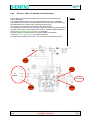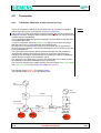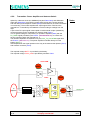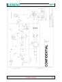
1
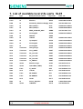
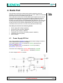
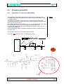
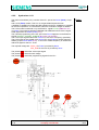
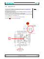
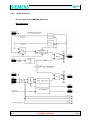
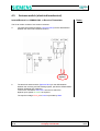
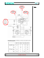
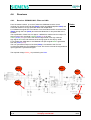
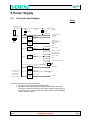
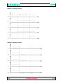
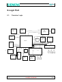
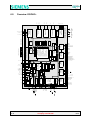
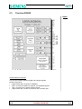
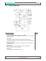
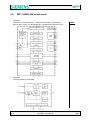
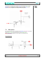
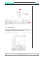
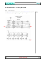
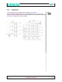
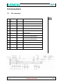
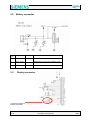
SL45
Level 2.5e
Repair Documentation
V 1.0
by Toko ([email protected])
V1.0
SL45
Page 1 of 43
Company Confidential
ICM MP CC ST
10/01
Table of Contents:
1. LIST OF AVAILABLE LEVEL 2,5E PARTS SL45 .............................................. 4
2. REQUIRED EQUIPMENT FOR LEVEL 2,5E SL45.............................................. 5
3. REQUIRED SOFTWARE FOR LEVEL 2,5E SL45 .............................................. 5
4. RADIO PART ....................................................................................................... 6
4.1.
Power Supply RF-Part.......................................................................................................................... 6
4.2.
Frequency generation ........................................................................................................................... 7
4.2.1.
Synthesizer: The discrete VCXO (13MHz) .................................................................................... 7
4.2.2.
Synthesizer: LO1............................................................................................................................. 8
4.2.3.
Synthesizer: LO2............................................................................................................................. 9
4.2.4.
Synthesizer: PLL........................................................................................................................... 10
4.3.
Antenna switch (electrical/mechenical) ............................................................................................. 11
4.4.
Receivers .............................................................................................................................................. 13
4.4.1.
Receiver: GSM900/1800 –Filter and LNA ................................................................................... 13
4.4.2.
Receiver : Mixer, IF Amplifier and Demodulator......................................................................... 14
4.4.3.
Smarti IC Overview ...................................................................................................................... 15
4.5.
Transmitter.......................................................................................................................................... 16
4.5.1.
Transmitter: Modulator and Up-conversion Loop ........................................................................ 16
4.5.2.
Transmitter: Power Amplifier and Antenna Switch...................................................................... 17
5. POWER SUPPLY............................................................................................... 19
5.1.
Overview and Voltages ....................................................................................................................... 19
5.2.
STV-Schalke-ASIC ............................................................................................................................. 20
5.3.
Power Supply MP3 (LARA)............................................................................................................... 24
6.LOGIC PART ........................................................................................................ 25
6.1.
Overview Logic................................................................................................................................... 25
6.2.
Overview EGOLD+............................................................................................................................ 26
6.3.
Overview EGAIM ............................................................................................................................... 28
6.4.
Overview MMG ASIC ....................................................................................................................... 31
6.5.
MP3 (LARA) HW components .......................................................................................................... 32
6.6.
FLASH memory .................................................................................................................................. 33
6.7.
Real time clock inside the EGOLD+.................................................................................................. 33
6.8.
IrDA ..................................................................................................................................................... 33
V1.0
SL45
Page 2 of 43
Company Confidential
ICM MP CC ST
10/01
6.9.
SIM ....................................................................................................................................................... 34
7. ACOUSTICS ...................................................................................................... 34
7.1.
General................................................................................................................................................. 34
7.2.
Vibra..................................................................................................................................................... 34
7.3.
Microphone.......................................................................................................................................... 35
7.4.
Loudspeaker ........................................................................................................................................ 36
8. ILLUMINATION AND KEYBOARD:................................................................... 39
8.1.
Illumination ......................................................................................................................................... 39
8.2.
Keyboard ............................................................................................................................................. 40
9. CONNECTORS .................................................................................................. 41
9.1
I/O connector ....................................................................................................................................... 41
9.2
Battery connector................................................................................................................................ 42
9.3
Display connector................................................................................................................................ 42
9.4
MMI connector.................................................................................................................................... 43
V1.0
SL45
Page 3 of 43
Company Confidential
ICM MP CC ST
10/01
1. List of available level 2,5e parts SL45
ID-No
Type
Name(function)/Location
Rep-Code
Order No.
D100
IC
EGOLD+
4EGO
L36810-G6103-D670
D250
IC
SCHALKE_ASIC/Pow.Supply 4PSA
L36145-J4682-Y29
D400
IC
MP3 (LARA) 1
4LA1
L36820-C6118-D670
D401
IC
MP3 (LARA) 2
4LA2
L36820-U6068-D670
D470
IC
MMG_SCHALKE_ASIC
4MMG
L36145-J4681-Y54
D490
IC
Volt.Reg/RF
4REG
L36820-C6148-D670
D500
IC
SMARTI
4SMA
D550
IC
LNA/RF
4LNA
L36820-L6047-D670
N600
IC
Op.Amp/RF
4OPA
L36810-C6046-D670
N630
IC
Volt.Reg/RF
4REG
L36820-C6070-D670
N631
IC
Volt.Reg/RF
4REG
L36820-C6147-D670
V251
Transistor
Charge/Logic
4CHT
L36830-C1064-D670
V530
Transistor
VCO_SW/RF
4SWT
L36820-C6047-D670
V601
Transistor
PA_Cont./RF
4SWT
L36840-C4014-D670
V651
Transistor
PA_Cont./RF
4SWT
L36840-C4009-D670
V653
Transistor
PA_Cont./RF
4SWT
L36840-C2074-D670
V810
Transistor
13_AMP/RF
4SWT
L36840-C4039-D670
Z100
Quarz
EGOLD+/Logic
4OSC
L36145-F102-Y14
Z400
Quarz
Quarz/MP3 (LARA)
4OSL
L36145-F260-Y13
Z500
Filter
IF_360/RF
4IFF
L36145-K280-Y127
Z530
VCO
1LO/RF
4VC1
L36145-G100-Y32
Z555
Filter
RX-PCN/RF
4FI1
L36145-K280-Y167
Z556
Filter
RX-GSM/RF
4FI3
L36145-K280-Y160
Z570
VCO
TX/RF
4VCT
L36145-G100-Y32
Z650
IC
Power_Amplifier
4PAM
L36851-Z2002-A45
Z800
Quarz
13MHz/RF
4VCX
L36145-F220-Y4
V1.0
SL45
Page 4 of 43
Company Confidential
ICM MP CC ST
10/01
2. Required Equipment for Level 2,5e SL45
¾
¾
¾
¾
¾
¾
¾
¾
¾
¾
¾
¾
GSM-Tester
(CMU200 or 4400S incl. Options)
PC-incl. Monitor, Keyboard and Mouse
Bootadapter 2000 (L36880-N9241-A200)
Troubleshooting Frame P35 (F30032-A82-A1)
Power Supply
Spectrum Analyser (Advantest 3162)
RF-Probe incl. Power Supply (e.g. from Agilent)
Oscilloscope incl. Probe
RF-Connector (N<>SMA(f))
Power Supply Cables
Dongle (F30032-P28-A1)
BGA Soldering equipment
Reference: Equipment recommendation Level 2,5e
3. Required Software for Level 2,5e SL45
¾
¾
¾
¾
¾
¾
V1.0
SL45
Windows NT Version4
Winsui version1.22 or higher
Winswup
Windows software for GSM-Tester ( Cats or CMU-GO)
Software for 13MHz adjustment
Internet unblocking solution
Page 5 of 43
Company Confidential
ICM MP CC ST
10/01
4. Radio Part
The radio part converts the I/Q base band signals supplied by the logic
(EGOLD+) into RF-signals with characteristics as per the GSM recommendation
(transmission) which are radiated by the antenna.
Or the radio part converts the received GMSK signal supplied by the antenna
into IQ base band signals which can then be further processed by the logic
(EGOLD+). The radio part is designed for Dual Band operation and can
therefore serve the frequency bands EGSM900 and GSM1800. The radio part
can never transmit and receive in both bands simultaneously. However, the
monitor time slot can be selected independently of the frequency band.
Transmitter and receiver are of course never operated simultaneously.
Notes
The radio part consists of the following blocks:
•
•
•
•
•
•
Power supply (RF-Voltage regulators)
Synthesizer (partly located in SMARTI)
Receiver (partly located in SMARTI)
Transmitter (Up conversion loop partly located in SMARTI)
Transmitter (Power amplifier)
Antenna Switch
4.1. Power Supply RF-Part
Two voltage regulators (N630/631) with a nominal output voltage of 2.8V are
used, to perform the required “RF-Voltages”.
The voltage regulator N630 is activated via SLEEPQ provided by the
EGOLD+ (TDMA-Timer H13).
The voltage regulator N631 is activated via VCXOEN provided by
the EGOLD+ (Functional P7).
The name of the voltages are: a) VCC_SYN activated by VCXOEN
and b) VCC2_8 activated by SLEEPQ
For both voltages BATT+ is required.
V1.0
SL45
Page 6 of 43
Company Confidential
ICM MP CC ST
10/01
4.2.
Frequency generation
4.2.1.
Synthesizer: The discrete VCXO (13MHz)
The generation of the 13MHz signal is done in the SL45 via a discrete VCXO.
A Colpitts oscillator with a crystal Z800 and a post-switched buffer stage is used
as oscillator switch.
The subsequent oscillating circuit (C807,C817, L800) and the resistor R806
create a de-coupling of the synthesiser from interference signals coming from the
logic (SIN13M (functional M14)).
The oscillator frequency is controlled by the (AFC_PNM) signal which is generated
from the EGOLD+ (D100 (functional R3)) and the capacity diode V800.
To reduce the charging time of the low pass (R816, C816) the resistor R816 is
bridged by the diode V802
For the temperature control a temperature-dependent resistance R802 is placed
near the VCXO.
Notes
The required voltage VCC_SYN is provided by the N631
The picture 4211 shows the SIN 13M measured at TP120.
S ig n a lfo rm
EGOLD+
V 1 .3
1
2
3
V 602
A FC
47K
100N
C110
30K
B AS170W
R615
GND
3
R600
22K
GND
10N
A FC_PN M
C600
2
100N
R106
C616
1
GND
4211
E-Gold+
V1.0
SL45
Page 7 of 43
Company Confidential
ICM MP CC ST
10/01
4.2.2.
Synthesizer: LO1
The first local oscillator (LO1) consists of the PLL part of the Smarti (D500), a loop
filter
and a VCO (Z530) module. This LO1 circuit generates frequencies from
1445MHz to 1520MHz for GSM 1800 RX-operation and from 1285MHz to 1361MHz
for the other operations. It is switched to select the channels in stages of 200kHz.
The VCO module is switched on by the EGOLD+ signal PLLON (TDMA-Timer J12)
via (V530). The switching between GSM900 and GSM1800 is done via the signal
OSW signal from the Smarti (D400 pin 21),
The channel programming of the PLL part of the Smarti happens via the EGOLD+
signals SYGCCL, SYGCDT, SYNSTR (RF Control K14, K15, M15).
The VCO output signal enables the Smarti IC to mix the IF-Frequency (360 MHz)
The VCO output is also guided to the Smarti PLL part (D400) to ensure frequency
stability (output Smarti D500 pin 20). To do so the 13MHz frequency is used as the
reference signal for the PLL circuit.
Notes
The required voltage are: VCC2_8 for D400 is provided by N630.
VCC_SYN for the VCO is provided by N631
The picture 4221 shows the VCO output signal
The picture 4222 shows Control voltage
The picture 4223 shows the programming signals for the PLL
4223
4221
V1.0
SL45
Page 8 of 43
Company Confidential
4222
ICM MP CC ST
10/01
4.2.3.
Synthesizer: LO2
The second local oscillator (LO2) consists of the PLL part of the Smarti (D400),
2 internal VCO´s (1440 MHz for RX-Mode and 1696 MHz for TX-Mode) and an
external filter (C509,C510,R501),
Both frequencies are divided by 4 to get the 360MHz demodulator IF frequency and
the 424MHz modulator frequency.
The RX/TX switching is done internally and is initiated by the EGOLD+ through the
SYGCCL, SYGCDT,SYNSTR (RF Control K14, K15, M15) signals.
Responsible for switching “On/Off” the second local oscillator in the EGOLD+ signal
PUPLO2 (TDMA-Timer L11) at SMARTI pin 16.
Notes
The required voltage VCC2_8 for D400 is provided by N630
The picture 4231 shows the VCO output signal
4231
External
filter LO2
VCO
LO2
PUPLO2
V1.0
SL45
Page 9 of 43
Company Confidential
ICM MP CC ST
10/01
4.2.4.
Synthesizer: PLL
PLL as a part of the PMB6250 (Smarti) IC
Blockdiagramm
V1.0
SL45
Page 10 of 43
Company Confidential
ICM MP CC ST
10/01
4.3.
Antenna switch (electrical/mechenical)
Internal/External <> GSM900/1800 <> Receiver/Transmitter
Notes
The SL45 mobile consists of two antenna switches.
a:
The mechanical antenna switch (connector X675) for the differentiation
between the internal and external antenna
from/to
diplexer
b:
The electrical antenna switch (Diplexer Z670) for the differentiation
between the receiving and transmitting signals, just like the differentiation
between GSM900 and GSM1800.
To do so the Transistors V672,V673 are used to switch the
diplexer input signals VC1–VC4 as required.
The required voltage VCC2_8 for D400 is provided by N630
V1.0
SL45
Page 11 of 43
Company Confidential
ICM MP CC ST
10/01
from/to
antenna
to receiver
GSM900
Notes
to receiver
GSM1800
GSM900
from PA
GSM1800
The matrix below shows the different conditions at the Diplexer and the
accompanying signals.
V1.0
SL45
Page 12 of 43
Company Confidential
ICM MP CC ST
10/01
4.4.
Receivers
4.4.1.
Receiver: GSM900/1800 –Filter and LNA
From the antenna switch, up to the IF-Mixer the GSM1800 receiver circuit
consists of a ceramic front end filter (Z555),a LNA (Low Noise Amplifier D550) and
a discrete distortion LC-high-pass-filter after LNA amplification.
For GSM900 the signal flow is as follows: From the antenna switch via a SAW filter
(Z556) through the LNA (D550) and a discrete distortion LC-low-pass-filter to the
IF-Mixer.
The amplification of both LNA´s is approx. 18dB with a matched 50 ohm output. To
switch on the LNA, the signal LNAON (Smarti pin 36) is used.
LNAG (Smarti pin 33) is in use if the received signal level is too high. With the
high signal LNAG the LNA reduces the incoming signal in one step by 20dB
For activating the GSM1800 or the GSM900 LNA part a signal BSW is generated
from the (Smarti pin 37)
The non-symmetrical output of the LNA (D550) is connected to the IF mixer
via a discrete balancing and adaptation circuit This circuit converts the asymmetrical
input signal into a symmetrical signal.
Notes
The required voltage VCC2_8 is provided by the N630
4415
4412
4411
4414
4413
V1.0
SL45
Page 13 of 43
Company Confidential
ICM MP CC ST
10/01
4.4.2.
Receiver : Mixer, IF Amplifier and Demodulator
The Smarti IC (D400) has two separate input mixers one for EGSM900 and
one for GSM1800.
The mixing result for both mixers is an intermediate frequency from 360 MHz.
The GSM900 mixer works in inverted sideband mode (LO1 above RX frequency),
the GSM1800 mixer in step mode (LO1 below RX frequency).
The outputs of both mixer are connected to the same IF Filter.
After passing an external IF Filter (Z500) the signal arrives at the programmable IF
amplifier in the Smarti. This amplifier has a dynamic of 80dB (-20dB to 60dB) and
can be set (PGCSTR;SYGCDT;SYGCCL) in 2dB steps.
Finally the signal is mixed down by the IQ demodulator to differential
I and Q (RX_I,RX_IX-RX_Q,RX_QX) signals off 50mVpp.
This signals are guided to the EGold+ A/D converters in the base band path.
Notes
4423
4421
to
EGold+
from LNA
4424
V1.0
SL45
4422
Page 14 of 43
Company Confidential
ICM MP CC ST
10/01
4.4.3.
Smarti IC Overview
Not active
V1.0
SL45
Page 15 of 43
Company Confidential
ICM MP CC ST
10/01
4.5.
Transmitter
4.5.1.
Transmitter: Modulator and Up-conversion Loop
The SL45 modulation is based on the principle of the up-conversion modulation
phase locked loop and is accomplished via the Smarti IC(D400).
The Smarti IC provides the quadratic modulator working with the TX IF frequencies
GSM/PCN 424 MHz. Whereby these frequencies are supplied from the second local
oscillator signals (1694MHz/4).
This so generated GMSK RF signal is compared in a phase detector with the down
mixed GMSK RF output.
To get the comparison signal the TXVCO_OUT signal is mixed with LO1 signal.
With the help of the 1.LO the GMSK-RF signal appearing at
the output of the TXVCO (Z570) is mixed to a TX IF below the TX signal and is
led on to the phase detector. The I-Q modulated signal in the IF position is also led
to the phase detector.
The output signal of the phase detector passes a discrete loop filter realized by
capacitors and resistors and force the TXVCO to work on the right frequency.
This large loop band width guarantees that the regulating process is considerably
quicker than the changes in the modulation signal.
The TXVCO is a so-called two-in-one VCO, this means the VCO module contains
the GSM900-VCO and the GSM1800-VCO in one housing.
The TXVCO is switched from GSM to PCN by using the signals GSM_TX_VCOENQ
and PCN_TX_VCOENQ from the EGold+ (TDMA Timer J13, K12)
Notes
The required voltage VCC2_8 is provided by N630
The required voltage VCC_SYN is provided by N631
1.LO
1285-1361 MHz
2.LO
1696 MHz
424 MHz
:4
880-915 MHz
1710-1785 MHz
424 MHz
Phase
Detector
TX-VCO
424 MHz
IQ
Modulator
TP
Mod Signal
4513
V1.0
SL45
4512
4511
Page 16 of 43
Company Confidential
ICM MP CC ST
10/01
4.5.2.
Transmitter: Power Amplifier and Antenna Switch
Splited by a discrete circuit into GSM900 (low pass R651/L650) and GSM1800
(high pass R652/C651) the TXVCO output signal arrives at the power amplifier.
The dual band power amplifier module (Z650) is assembled on a ceramic substrate
in one housing. The module amplifies the output signal of the TXVCO to the
required PCL. Controlled by the feedback circuit according to settings from the
logic.
A part of the TX output signal is decoupled via a directional coupler (realised by
conductive tracks) and is equalised at a detector diode (V620).
This so gained voltage is compared by an operation amplifier (N600) with the
PA_RAMP signal provided by the EGold+ (GAIM/BASEBAND H2), to ensure that
the PA is working within the required PCL´s.
The different amplifiers are selected on by the PCN_TX_VXCOENQ signal from
the EGold+ (TDMA Timer K12). The power amplifier is feeded directly from the
battery (BATT+).
After amplification the signal passes on the way to the antenna the diplexer (Z670)
and antenna connector (X675).
Notes
The required voltage BATT+ is provided by the battery.
The required voltage VCC2_8SW is provided by transistor V600.
VCC2.8SW
4523
PA_RAMP
Batt+
to
diplexer
4524
4521
4522
TXVCO_OUT
PF08112B
V1.0
SL45
Page 17 of 43
Company Confidential
ICM MP CC ST
10/01
V1.0
SL45
Page 18 of 43
Company Confidential
ICM MP CC ST
10/01
5. Power Supply
5.1.
Overview and Voltages
Notes
Leerlaufspannung 1) :
4,3V..3,2V
47 µF
(in Logik)
Ri
1,6 A
im TX
PA
+Treiber
+Regelung
22 µF
(an PA)
110 mA max.
Li Thin-Ion
540mAh
Linear2,0V +-5%
Regler
10mA max.
[SCHALKE_ASIC]
VDDRTC
EGOLD+ Core
MMG SCHALKE_ASIC
4Mbit SRAM
Flash
2,07V +-3%
LinearRegler
140mA max.
[SCHALKE_ASIC]
Linear2,65V +-3%
Regler
220mA max.
[SCHALKE_ASIC]
1mA max.
20mA max.
60mA max.
Linear2,9V +-2%
Regler
140mA max.
[SCHALKE_ASIC]
55mA+6mA
5mA
50mA max. 3)
1) bei Akku ziehen:
6,5V max. für ?s
2) Intel 55mA max.
ST 20mA max.
3) 3201: 32mA typ.
2,9V +-4%
LinearRegler
extern
2,8V +- 3,5%
LinearRegler
extern
100mA max.
100mA max.
EGOLD+ Portpin
Vibrator (evtl. an Batt+)
Flash 2) + SIM
MMC
MMG-SCHALKE_ASIC I/O
IrD
LED
100mA max.
75 mA max.
2,8V +- 3,5%
100mA max.
Display
EGOLD+ Ringing
150mA + 20mA. (16Ohm HK+GAIM)
50mA
LinearRegler
extern
Beleuchtung Display
+ Tastatur
LARA (MP3)
RX,
RF Synth /
45 mA max.
The following restrictions must be observed:
• The phone cannot be operated without battery.
• The phone will be damaged if the battery is inserted the wrong way
round (the mechanics of the phone prevent the battery from being put
in the wrong way round). The electric system assumes that the battery
as been inserted correct.
V1.0
SL45
Page 19 of 43
Company Confidential
ICM MP CC ST
10/01
5.2.
STV-Schalke-ASIC
The power supply Schalke-ASIC contains the following functions:
•
Notes
Control of “switching on” the mobile phone via
1.The ON/OFF Key. (Schalke-ASIC F4)
2.The bottom connector with the signal VDD_CHARGE (Schalke-ASIC A4)
3.The Real Time Clock RTC_Int (Schalke-ASIC F5)
•
Watchdog monitoring
1.Control of “switching off” the mobile phone via WATCHDOG_µP.
2. Watchdog observation
•
•
•
•
•
•
Switch off of mobile phone in the case of overvoltage at battery connection.
Generation of RESET signal for EGOLD+, Flash, MMG_ASIC and
Display
Generation of 2.90 V via linear controller (REG_1)
Generation of 2.00 V via linear controller (REG_2)
Generation of 2.65 V via linear controller (REG_3)
Generation of 2.00 V via linear controller (LPREG)
•
Analog switches
7.
7.
7.
7.
•
•
•
Battery charge support:
1. Normal charging
2. Trickle charging, if the battery voltage is below 3,2 V.
Timer generation
All internal timers and pulses are derived from a 900 kHz ± 10% internal
oscillator. Responsible for the frequency stability is an external resistor
(R257) (1%) at the RREF pin.
Audio
1.
2.
3.
4.
•
SIM Switch
LIGHT Switch
IRDA Switch
VSPG_Teiler Switch
Audio amplifier
Mono audio driver for internal loudspeaker
Driver to generate ringer tones
Key-click generator
I2C bus for communication between EGOLD+ and Schalke-ASIC
V1.0
SL45
Page 20 of 43
Company Confidential
ICM MP CC ST
10/01
Switch on timing overview
Switch off timing overview
V1.0
SL45
Page 21 of 43
Company Confidential
ICM MP CC ST
10/01
Battery
A Li-Ion battery with a nominal capacity of 540mAh is used for SL45.
A temperature sensor (NTC) is integrated to monitor the battery temperature.
Notes.
Charging Concept
General
To control the charging process a charging control unit consists of a Fast Charge
Controller and a Trickle Charger is implemented. Existing of a internal current
source, a temperature monitoring, a external charge-FET, a charge detector
( voltage level and/or charge current of an external charger supplied trickle charge
circuit) and a detection of the charge current in 5 steps.
The charging control unit communication with the EGOLD+ is done via the I2C bus.
•
•
•
•
•
•
CHARGE_µC: charge request input of the EGOLD+
CHARGE: Open Drain, -300...-600µA
TBAT: comparator input for temperature sensor of the battery
REF_EXE: Reference voltage for temperature sensor
VDD_CHARGE: Charger typ detector input, power supply for trickle charge
SENSE_IN: Voltage input of external current sensor (with reference to AVDD)
With rising slope on CHARGE_µC the current source is switched on via a LOW
active CHARGE signal and the Charge-FET is conductive.
Condition:
- CHARGE_µC is HIGH for min. 20µs
- temperature sensor detects no overhead
- No overvoltage on VDD.
With falling slope on CHARGE_µC the current source is switched off and the
Charge-FET is locked.
Temperature sensor works by T>60°C.
Fast charging
After connecting a charger and a battery voltage higher then 3,2 V the controller
switches via a HIGH level of CHARGE_µC the charge-FET conductive, if the level
of TBAT is > then the level of REF_EXE.
The charging current (and battery voltage) is controlled with the pulse duty factor of
CHARGE_µC. The current flow can detected with the signal SENCE_IN, controlled
via the I2C bus from the EGOLD+.
Trickle charge
If the phone has not been used for a longish time (longer than approx. 1 month), the
battery could be totally self-discharged. (battery voltage less then 3,2V), so that
it is not possible to charge the battery via the normal charging circuit. In this case
only trickle charge is possible.
The Schalke-ASIC controlles the charging circuit himself.
Battery voltage below 2,8 Volt charging current 20mA.
Battery voltage below 3,2 Volt charging current 50mA.
Battery voltage over 3,2 Volt “Normal charging”.
Power supply for the Schalke-ASIC in this mode is the external charger.
(VDD_CHARGE) This charging mode is not visible for the customer. IF the battery
voltage reaches the 3,2V level the Schalke-ASIC switch into normal charge.
V1.0
SL45
Page 22 of 43
Company Confidential
ICM MP CC ST
10/01
Measurement of Battery and Ambient Temperature
Notes
The voltage equivalent of the temperature on the voltage divider is measured
as the difference against a reference voltage of the EGOLD+. For this, the
integrated Σ∆ converter of the EGOLD+ of the RX-I base band branch is used.
Via an analog multiplexer, either the RX-I base band signal,(the battery temperature
Voltage) or the ambient temperature voltage can be switched to the input of the
converter. The 1-Bit current of the converter will be subjected to a data reduction via
the DSP circuit so that the measured voltage (for battery and ambient temperature)
will be available at the end as a 10-bit data word.
Measurement of the Battery Voltage
Analog to the I-branch either the RX-Q base band signal or the battery voltage can
be measured in the Q-branch. The processing in the DSP circuit is done similar to
the I-branch. The EGOLD+ is specified for voltages measurements at the input
pin N1 (VBAT) from 3V...5.5V.
Timing of the Battery Voltage Measurement
Unless the battery is going to be charged, the measurements are made in the
TX time slot. While charging the measurement is done after the TX time slot.
At the same time, either the battery temperature (in the I-branch) and the
battery voltage (in the Q-branch) or the ambient temperature in the I-branch can be
measured
Other combinations are not possible. For the time of the measurement
the multiplexer in the EGOLD+ must be programmed to the corresponding
measurement.
V1.0
SL45
Page 23 of 43
Company Confidential
ICM MP CC ST
10/01
5.3.
Power Supply MP3 (LARA)
A voltage regulator (N490) with a nominal output voltage of 2.9V is
used, to perform the required MP3 (LARA) voltage.
The voltage regulator N490 is activated via MP3 (LARA) _EN provided by the
EGOLD+ (RF-Control L12).
The name of the voltages is 2V9_MP3 (LARA) activated by MP3 (LARA) _EN
For the voltage BATT+ is required.
V1.0
SL45
Page 24 of 43
Company Confidential
ICM MP CC ST
10/01
6.Logic Part
6.1.
Overview Logic
Flash
Display
CS_FLASH
CS_SRAM, BHE
32Mbit
80x101
A(0:22), D(0:16), RD, WR
MMC
MMG
CS_MMG
MMCCLK,
inkl.
MMCDAT,
MMCCMD
3Mbit SRAM
IRQ_MMG, SYSCLK
MMCVCC
RESET_2.0V
MMCSW
CS_LCD, RS_LCD,
CLI,
SCL, SI
SIC,
SID,
LARA (MP3)
I²S
DAT_REQ
Keyboard
WSI,
DAI
3V
KB0:KB9
ON_OFF=KB9
LARA (MP3)_EN
LDO
LARA (MP3)-
3V
Dek.
3V
I²S
DAC
EGOLD+
I²C EPP2/EPN2
Radio-
LS_LEFT,
part
RESET_2.65V
s. Schnittstelle HF-Logik
LS_RIGHT
s. I/O-Schnittstelle
CHARGE_uC
WA_DOG,
RTC_INT,
SLEEP, LOW_BATTERY
I/O
VCXO_EN
VIBRA_ON
IR_TX
IRDA_OFF
BATT+
CCCLK,
AKKU
6 Register I2C
LDO 1,92V
LDO 2,65V
GAIM-
CCRST,
CCIO
IrDa
SIM-Switch
VSPG_TEILER
IR_RX,
I2CI
EPP1_FIL/EPP2_FIL
CCVZQ
GAIMLDO 2,9V
Voltage-
Schalter
divider
RTC-LDO 2,0V
Schalke
2,9V
ON_OFF
CCVCC
Power
Laden,
Licht-PWM
Trickle Charge
Dimmen
SIM
3V
LIGHT
1,8V
Vibra
MICP1,
EPP2
EPP1,
MICN1
LEDs
Battery
540mAh
Li-Ion
Key/
Displayillumination
Vertraulich - Confidential
V1.0
SL45
Page 25 of 43
Company Confidential
ICM MP CC ST
10/01
AFC
CS2 / CC02IO / PF.12
CS3 / EX4IN & DSPIN0 & T4EUD / PF.13
CS4 / DSPOUT2 / PF.14
CS0
CS1
BHE / CC00IO / PF.15
RD
WR
RSTOUT / EX6IN & T3EUD / PF.2
A(20:0)
D(7:0)
D8 / CC20IO / PA.8
D9 / CC16IO / PA.9
D10 / - / PA.10
D11 / - / PA.11
D12 / EX5IN / PA.12
D13 / T7IN / PA.13
D14 / CC22IO / PA.14
D15 / CC18IO / PA.15
TRIGOUT
TRIGIN
MON2
MON1
READY / WAKEUP / PC.1
CC02IO / - / HOLD & DSPOUT1 / PF.0
CC01IO / NMI & DSPOUT2 / PE.2
HLDA / CC03IO & DSPIN0 & T2IN / PC.3
T5IN / T2EUD & T3IN / PC.4
CC06IO / A21 & EX7IN / PF.11
CLKOUT / CC05IO / PC.0
DSPOUT1 / A22 / PF.1
CC00IO / T3OUT / PC.2
RESET_IN
3
5
24
21
2
16
8
8
8
16
Osc.
VDDRTC
4
Keypad
Interface
6
Pulse-Carry Mod.
AFC Unit
CS(4:0)
External
Bus & Port
Controller
Multicore
Debug Support
6
ID Register
2 x 8 bit
CAPCOM
RTC
SSC
ASC0
ASC1
High Speed
(F=512, D=8/16)
SIM card
Interface
60
CLKSXM / A21 / PF.5
CLKANA
MCU
Power
Management
Peripheral Enable
Generator
SRAM
VSSa
to MCU &
Clock Generation Unit
xk x 16 (x = 0...64)
1k x 16
PROM
1k x 16
PRAM
1k x 16
Dual Port RAM
Interrupt Controller
DPEC
C166CBC
OCDS
PDOUT / A23 / PF.4
Clock Generation
F13M
13 MHz / 32 kHz
READY#
NMI#
HOLD#
HLDA#
CLKOUT
RSTOUT#
Watchdog
GPT1/GPT2
Autobaud
Detect
Interrupt
Extension
PD-Bus
32 kHz
SPI
compatible
CCLK
32.768 kHz
CCRST
F32K
KP9 / CC18IO / PB.9
KP8 / CC22IO / PB.8
KP7 / T7IN / PB.7
KP6 / EX5IN / PB.6
RTCOUT
KP5 / - / PB.5
KP4 / - / PB.4
KP3 / CC16IO / PB.3
KP2 / CC20IO / PB.2
KP1 / CC06IO / PB.1
KP0 / T2EUD & EX0IN / PB.0
TXD0 / - / PE.4
RXD0 / - / PE.3
CCVZ / - / PB.10
2
CCIN
MRST / - / PE.7
MTSR / - / PE.6
SSCCLK / - / PE.5
CCIOSW / T6OUT & T0IN
& T6IN / PB.11
TXDD / TXD1 / PF.6
TFSD / T2IN / PF.10
SCLK / T6EUD / PF.8
RFSD / - / PF.9
RXDD / RXD1 / PF.7
CCIO
VDDa
Boot
Block
16 bit I/O Ports
SEIB
OCEM
9
TDMA Timer
GSM
5
Bus
Interface
Unit
Interrupt Controller
Interleaving
2 x 28 x 116 x 1
16 bit write access
4/16 bit read access
De-Interleaving 12k x 4
3
RF Control
4
Dual Port 512 x 16
3
X RAM
6k x 16
X ROM
18k x 16
Y RAM
2k x 16
P RAM
5k x 16
P ROM
48k x 16
A51/52
Cipher
Unit
Audio & Speech
Shared Memory
DSP Timer2
OAK+ DSP
DSP Timer1
Viterbi
HW
Accelerator
x Interleaving / De-Interleaving
x Speech Decoding (FR, HR, EFR)
x Speech Coding (FR, HR, EFR)
x Level Measurement
x Channel Decoding (FR, HR, EFR)
x Channel Coding (FR, HR, EFR)
x Equalization
x Encryption / Decryption
x Voice Memo / Voice Dialing
Enable Signals to
X- and PD-Bus
Peripherals
E-GOLD Architecture
52 MHz
X-Bus
VCXO_EN / - / PE.8
T_OUT12 / A23 / PD.11
T_OUT11 / CC19IO / PD.10
T_OUT10 / EX1IN & DSPIN1 / PD.9
T_OUT9 / T7IN & EX3IN / PD.8
T_OUT8 / CC23IO / PD.7
T_OUT7/ CAPIN / PD.6
T_OUT6 / T4IN / PD.5
T_OUT5 / CC17IO / PD.4
T_OUT4 / DSPIN0 / PD.3
5
T_OUT3
T_OUT2
T_OUT1
T_OUT0
GAIMRXON
2
GAIMDATA
GAIMSTR
GAIMCLK
3
RFSTR4 / EX2IN / PD.2
RFSTR3 / CC18IO / PD.1
RFSTR2 / CC07IO / PD.0
requires ext. crystal
and special bondout
5
TXD1 / CC04IO / PE.0
Boundary Scan
JTAG
TAP Controller
GMSK Modulator
Baseband Filter
RX and TX
Voiceband Filters
Enhanced Handsfree / DAI
DSP Serial
Communication
Interface
RXD1 / EX1IN & T5EUD /
PE.1
2 MHz (to GAIM)
Core
Company confidential
VDD1.(2:0)
H. Meschede, HL AS CR CE,
RFSTR1
RFSTR0
RFDATA
RFCLK
DSPOUT0 / A22 / PF.3
VSS1.(2:0)
Page 26 of 43
Company Confidential
VDD2.(4:1)
VDD2.0x, x=a,b,c
V1.0
SL45
I/O Driver
VSS2.(4:1)
VSS2.0x, x=a,b,c
TDO
TDI
TCK
TMS
TRST
DACQ
DACI
BPDM2
BPDM1
VCLK
VBOUT
VBIN
6.2.
Overview EGOLD+
ICM MP CC ST
10/01
Notes
The µC-part components
•
•
•
Mikrocontroller
Systeminterfaces for internal and external peripherals
Onchip peripherals and memory chips
The Controller-Firmware:
•
Controlling of the Man Machine Interface
(Keypad, LCD, Illumination, ... )
• GSM Layer 1-3
• Controlling Radio part (Synthesizer, AGC, AFC, ...),
• Controlling of the Baseband part (EGAIM)
The SP-Part components
•
DSP Signalprozessor
Die DSP-Firmware
•
•
•
•
•
Equaliser
Channel Coder
Channel Decoder,
Voice Encoder
Voice Decoder
V1.0
SL45
Page 27 of 43
Company Confidential
ICM MP CC ST
10/01
6.3.
Overview EGAIM
Notes
EGAIM inside the EGOLD+
This IC is the interface between digital and analogue signals.
EGAIM components
•
•
•
•
2 Sigma Delta A/D-converter for RX/Battery
2 D/A- converter for GMSK TX Inphase- und Quadratursignals,
1 D/A- converter for the Power Ramping signal,
1 Sigma Delta A/D- und D/A-converter for the voiceband part
V1.0
SL45
Page 28 of 43
Company Confidential
ICM MP CC ST
10/01
a) Measurement of Battery and Ambient Temperature
The temperature is measured as a voltage equivalent of the temperature on the
voltage dividers R115,R116,R117 for the battery temperature and R118,R119,
R120 for the ambient temperature from the EGAIM.
For this, the integrated Σ∆ converter of the EGAIM of the RX-I base band
branch is used. This Σ∆ converter compares the voltage of TBAT and TENV
internally with a reference voltage BREF.
Via an analog multiplexer, either the RX-I base band signal, or the TBAT signal
and the TENV signal can be switched to the input of the converter.
The signal MEAS_ON from the EGOLD+(GSM TDMA-TIMER G11) activates the
measurement and is used to generate to BREF by the help of R121,R122
Notes
b) Measurement of the Battery Voltage
The measurement of the battery voltage is done in the Q-branch of the EGAIM.
For this BATT+ is connected via a voltage divider R113, R114 to the EGOLD+
(GAIM N2) (Input limitation 1.33V to 5.91V) .An analog multiplexer does the
switching between the baseband signal processing and the voltage
measurement.
V1.0
SL45
Page 29 of 43
Company Confidential
ICM MP CC ST
10/01
a) A/D conversion of MIC-Path signals incl. coding
The Microphone signals (HF_MICRO, MICN2, MICP, MICN) arrive at Notes
the voiceband part of the EGAIM. For further operations the signals will
be converted into digital information, filtered, coded and finally formed
into the GMSK-Signal by the internal GMSK-Modulator.
This so generated signals (IT, ITX, QT, QTX) are given to the SMARI IC
(pins 9-12) in the transmitter path.
b) D/A conversion of EP-Path signals incl. decoding
Arriving at the Baseband-Part the demodulated signals (RX_I, RX_IX, RX_Q,
RX_QX) will be filtered and A/D converted. In the voiceband part after decoding
(with help of the uC part) and filtering the signals will be D/A converted amplified
and given as (EPP1, EPN1, EPP2, EPN2) to the internal earpiece or the external
loudspeaker.
c) Generation of the PA Control Signal (PA_RAMP)
The RF output power amplifier needs an analog ramp up/down control voltage.
For this the system interface on EGOLD+ generates 10 bit digital values which
have to be transferred serially to the power ramping path. After loading into an
10 bit latch the control value will be converted into the corresponding analog
voltage with a maximum of ~2V
Key-Value
V1.0
SL45
Page 30 of 43
Company Confidential
ICM MP CC ST
10/01
6.4.
Overview MMG ASIC
Notes
MMG-ASIC components
•
Frequency generation
The PLL generates a 52MHz signal based on the 13MHz(output CLKSXM EGOLD+). The signal is the reference of all Clock and Timing
signals of the ASIC.
•
I²S-Interface:
The interface modulate the data of the DAI-Interfaces (EGOLD+) into a
I2S-data format, used for the input of the stereo-D/A-converter in the DAC3550.
•
MP3 (LARA) - Interface:
Generate a MP3 (LARA) -data current. Conversation of parallel-/serial data of
the 16bit-parallelbus
•
MMC-Interface:
Access to the MMC via serial HW-Interface. Control commands and
data transmission from and to the EGOLD+.
•
3MBit SRAM:
SRAM implemented for write and read access.
V1.0
SL45
Page 31 of 43
Company Confidential
ICM MP CC ST
10/01
6.5.
•
MP3 (LARA) HW components
DAC3550
Stereo-D/A-converter analogue - multiplexer are inside, for speech and
MP3 (LARA) output. (not simultaneously). Loudness level adjusted via I²C.
•
Notes
MAS3507
Decoding off MP3 (LARA) data
V1.0
SL45
Page 32 of 43
Company Confidential
ICM MP CC ST
10/01
6.6.
FLASH memory
Non volatile, but erasable and re-programmable (Software-Update) memory chip
of the EGOLD+, also to save user data (menu settings), Voice Memo,
adjustment values
6.7.
Notes
Real time clock inside the EGOLD+
Real time clock, supplied from a voltage regulator inside the Schalke-ASIC.
Also active when mobile phone is switched off. During battery change a
capacitor (C258) as power supply is used for minimum 30 sec to save
the stored data.
6.8.
IrDA
Infrared diode for data transfer to standard IrDa devices.
V1.0
SL45
Page 33 of 43
Company Confidential
ICM MP CC ST
10/01
6.9.
SIM
SIM cards support of 1.8V and 3V cards.
Notes
7. Acoustics
7.1.
General
The Electro-Acoustic components are: a) Vibra
b) Microphone
c) Loudspeaker
d)Ringer
7.2.
Vibra
The Vibra is driven and controlled from the EGOLD+ (Miscellaneous M6)via the
signal Vibra_ON.
V1.0
SL45
Page 34 of 43
Company Confidential
ICM MP CC ST
10/01
The vibrator is activated by the transistor V290 via the Signal Vibra_on from
EGOLD+. Batt+ is required to provide the VIBRA. The diode V292 is used
to protect the circuit against over voltage and switching spikes.
7.3.
Notes
Microphone
Both Microphones are direct connected to the EGOLD+.(Voiceband F1-F4) via the
signals MICN1, MICP1 (Internal Microphone )and MICN2, MICP2
(External Microphone/Headset). Power supply for the Microphone is
VMIC (Voiceband E1)
Internal Microphone
V1.0
SL45
Page 35 of 43
Company Confidential
ICM MP CC ST
10/01
Notes
External Microphone
7.4.
Loudspeaker
The internal Loudspeaker (Earpiece) is connected to the voiceband part of the
EGOLD+ (VOICEBAND C1,D2) via the mono audio amplifier inside the Schalke-ASIC.
Also the ringing tones are generated with the loudspeaker.
Signal names:
V1.0
SL45
EGOLD+ - Schalke-ASIC
EPN1_FIL - EPP1_FIL
Page 36 of 43
Company Confidential
ICM MP CC ST
10/01
Signal names:
Schalke-ASIC - Speaker
EPP1 - EPN2
Notes
The external Loudspeaker (Headset) is connected to the voiceband part of the
EGOLD+ (VOICEBAND D1,E2) (EPN/EPP2)via the Stereo-D/A-converter
analogue - multiplexer inside the DAC3550.(HS_LEFT/HD_RIGHT)
V1.0
SL45
Page 37 of 43
Company Confidential
ICM MP CC ST
10/01
The SL45 has no ringer component. Responsible for the audio output of the ringer
tones is the loudspeaker. The ringer tones are generated by a signal RINGIN from
the EGOLD+ (Miscellaneous M11). This signal goes to the mono audio amplifier inside
the Schalke-ASIC.
V1.0
SL45
Page 38 of 43
Company Confidential
Notes
ICM MP CC ST
10/01
8. Illumination and keyboard:
8.1.
Illumination
The Light is switched via an analogue switch inside the Schalke-ASIC. It is controlled
from the EGOLD+ with the signal LIGHT_OFF. Output is the signal LIGHT which is
connected via the MMI connector the LEDs.
V1.0
SL45
Page 39 of 43
Company Confidential
Notes
ICM MP CC ST
10/01
8.2.
Keyboard
The keyboard lines are via MMI connector linked to the EGOLD+
(Keybad R7/R8/P8/N8/M8/N9/R10/P10/N10/R11). KB (keyboard line ) 0 to 5 are outputs,
KB 6 to 9 inputs. To make a short cut from an output to an input line with the keypad
the EGOLD+ registered with key is pressed.
V1.0
SL45
Page 40 of 43
Company Confidential
Notes
ICM MP CC ST
10/01
9. Connectors
9.1
I/O connector
Notes
Name
IN/OUT
Notes
HS_LEFT
I/O
Output left channel for stereo-headset.
3
POWER
I
Charging Current
4
FBatt+
O
Power supply for the accessories.
5
TX
O
Serial interface
6
RX
I
Serial interface
7
ZUB_CLK
I/O
8
ZUB_DATA
I/O
9
GND_MIC
Clock line for accessory bus
Use as DTC In data operation
Data line for accessory bus.
Use as CTS in data operation
For external microphone
10
MICP2
I
External microphone
11
HS_RIGHT
O
Output right channel for stereo-headset
12
LGND
Pin
1
GND
2
V1.0
SL45
For external loudspeaker
Page 41 of 43
Company Confidential
ICM MP CC ST
10/01
9.2
Battery connector
Name
IN/OUT
Notes
Akku_Temp
O
Temperature control of the battery pack.
POWER +
I/O
Battery voltage
Pin
1
GND
2
3
9.3
Display connector
Connection Egold+ to
Display-Controller
V1.0
SL45
Page 42 of 43
Company Confidential
ICM MP CC ST
10/01
9.4
MMI connector
Function
ILLUMINATION
Names
Light
KEYBOARD
KB0 – KB9 / ON_OFF
IrDA INTERACE
IR_RX / IR/TX_BUFFER
BATTERY VOLTAGE
BATT+
V1.0
SL45
Page 43 of 43
Company Confidential
ICM MP CC ST
10/01