1
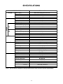
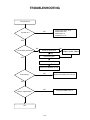
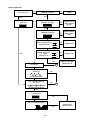
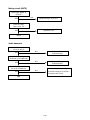
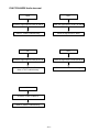
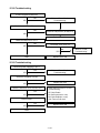
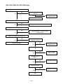
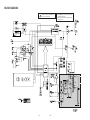
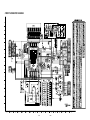
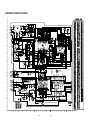
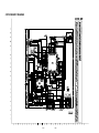
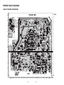
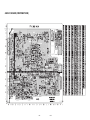
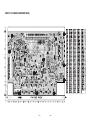
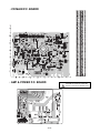
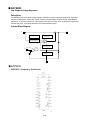
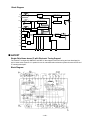
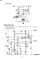
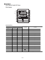
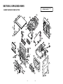
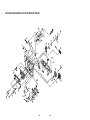
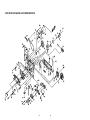
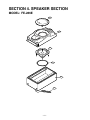
SERVICE MANUAL
MODEL: FFH-286A/AD, FE-286E
3CD CHANGER
HI-FI SYSTEM
SERVICE MANUAL
MODEL : FFH-286A/AD, FE-286E
CONTENTS
SECTION 1. GENERAL
• SERVICING PRECAUTIONS .................................................................................................................... 1-2
• ESD PRECAUTIONS ................................................................................................................................. 1-4
• SPECIFICATIONS ..................................................................................................................................... 1-5
SECTION 2. ELECTRICAL
• ADJUSTMENTS ......................................................................................................................................... 2-1
• TROUBLESHOOTING ............................................................................................................................... 2-3
• WAVEFORMS OF MAJOR CHECK POINT .............................................................................................. 2-7
• BLOCK DIAGRAM ................................................................................................................................... 2-17
• SCHEMATIC DIAGRAMS ........................................................................................................................ 2-19
• WIRING DIAGRAM .................................................................................................................................. 2-27
• PRINTED CIRCUIT DIARGAMS .............................................................................................................. 2-29
• INTERNAL BLOCK DIAGRAM OF IC’s ................................................................................................... 2-38
• REPAIRS REGARDING CD MECHANISM ............................................................................................. 2-45
SECTION 3. EXPLODED VIEWS
• CABINET AND MAIN FRAME SECTION ................................................................................................. 3-1
• TAPE DECK MECHANISM: AUTO STOP DECK(OPTIONAL) .................................................................. 3-3
• TAPE DECK MECHANISM: AUTO REVERSE DECK ................................................................................ 3-5
• CD MECHANISM ........................................................................................................................................ 3-7
SECTION 4. SPEAKER .................................................................................................................. 4-1
SECTION 5. REPLACEMENT PARTS LIST .................................................................................. 5-1
- 1-1 -
SECTION 1. GENERAL
SERVICING PRECAUTIONS
NOTES REGARDING HANDLING OF THE PICK-UP
1. Notes for transport and storage
1) The pick-up should always be left in its conductive bag until immediately prior to use.
2) The pick-up should never be subjected to external pressure or impact.
Storage in conductive bag
Drop impact
2. Repair notes
1) The pick-up incorporates a strong magnet, and so should never be brought close to magnetic materials.
2) The pick-up should always be handled correctly and carefully, taking care to avoid external pressure and
impact. If it is subjected to strong pressure or impact, the result may be an operational malfunction and/or
damage to the printed-circuit board.
3) Each and every pick-up is already individually adjusted to a high degree of precision, and for that reason
the adjustment point and installation screws should absolutely never be touched.
4) Laser beams may damage the eyes!
Absolutely never permit laser beams to enter the eyes!
Also NEVER switch ON the power to the laser output part (lens, etc.) of the pick-up if it is damaged.
NEVER look directly at the laser beam, and don’t let
contact fingers or other exposed skin.
5) Cleaning the lens surface
If there is dust on the lens surface, the dust should be cleaned away by using an air bush (such as used
for camera lens). The lens is held by a delicate spring. When cleaning the lens surface, therefore, a
cotton swab should be used, taking care not to distort this.
Pressure
Magnet
Pressure
How to hold the pick-up
Cotton swab
Conductive Sheet
6) Never attempt to disassemble the pick-up.
Spring by excess pressure. If the lens is extremely dirty, apply isopropyl alcohol to the cotton swab. (Do
not use any other liquid cleaners, because they will damage the lens.) Take care not to use too much of
this alcohol on the swab, and do not allow the alcohol to get inside the pick-up.
- 1-2 -
NOTES REGARDING COMPACT DISC PLAYER REPAIRS
1. Preparations
1) Compact disc players incorporate a great many ICs as well as the pick-up (laser diode). These
components are sensitive to, and easily affected by, static electricity. If such static electricity is high
voltage, components can be damaged, and for that reason components should be handled with care.
2) The pick-up is composed of many optical components and other high-precision components. Care must
be taken, therefore, to avoid repair or storage where the temperature of humidity is high, where strong
magnetism is present, or where there is excessive dust.
2. Notes for repair
1) Before replacing a component part, first disconnect the power supply lead wire from the unit
2) All equipment, measuring instruments and tools must be grounded.
3) The workbench should be covered with a conductive sheet and grounded.
When removing the laser pick-up from its conductive bag, do not place the pick-up on the bag. (This is
because there is the possibility of damage by static electricity.)
4) To prevent AC leakage, the metal part of the soldering iron should be grounded.
5) Workers should be grounded by an armband (1MΩ)
6) Care should be taken not to permit the laser pick-up to come in contact with clothing, in order to prevent
static electricity changes in the clothing to escape from the armband.
7) The laser beam from the pick-up should NEVER be directly facing the eyes or bare skin.
Armband
Resistor
(1 Mohm)
Resistor
(1 Mohm)
Conductive
Sheet
CLEARING MALFUNCTION
You can reset your unit to initial status if malfunction occur(button malfunction, display, etc.).
Using a pointed good conductor(such as driver), simply short the RESET jump wire on the inside of the
volume knob for more than 3 seconds.
If you reset your unit, you must reenter all its settings(stations, clock, timer)
NOTE: 1. To operate the RESET jump wire, pull the volume rotary knob and release it.
2. If you wish to operate the RESET jump wire, it is necessary to unplug the power cord.
VOLUME
UP
RESET jump wire
VOLUME KNOB
DOWN
- 1-3 -
ESD PRECAUTIONS
Electrostatically Sensitive Devices (ESD)
Some semiconductor (solid state) devices can be damaged easily by static electricity. Such components
commonly are called Electrostatically Sensitive Devices (ESD). Examples of typical ESD devices are integrated
circuits and some field-effect transistors and semiconductor chip components. The following techniques should
be used to help reduce the incidence of component damage caused by static electricity.
1. Immediately before handling any semiconductor component or semiconductor-equipped assembly, drain off
any electrostatic charge on your body by touching a known earth ground. Alternatively, obtain and wear a
commercially available discharging wrist strap device, which should be removed for potential shock reasons
prior to applying power to the unit under test.
2. After removing an electrical assembly equipped with ESD devices, place the assembly on a conductive
surface such as aluminum foil, to prevent electrostatic charge buildup or exposure of the assembly.
3. Use only a grounded-tip soldering iron to solder or unsolder ESD devices.
4. Use only an anti-static solder removal device. Some solder removal devices not classified as "anti-static" can
generate electrical charges sufficient to damage ESD devices.
5. Do not use freon-propelled chemicals. These can generate electrical charges sufficient to damage ESD
devices.
6. Do not remove a replacement ESD device from its protective package until immediately before you are ready
to install it. (Most replacement ESD devices are packaged with leads electrically shorted together by
conductive foam, aluminum foil or comparable conductive materials).
7. Immediately before removing the protective material from the leads of a replacement ESD device, touch the
protective material to the chassis or circuit assembly into which the device will by installed.
CAUTION : BE SURE NO POWER IS APPLIED TO THE CHASSIS OR CIRCUIT, AND OBSERVE ALL OTHER
SAFETY PRECAUTIONS.
8. Minimize bodily motions when handing unpackaged replacement ESD devices. (Otherwise harmless motion
such as the brushing together of your clothes fabric or the lifting of your foot from a carpeted floor can
generate static electricity sufficient to damage an ESD device).
CAUTION. GRAPHIC SYMBOLS
THE LIGHTNING FLASH WITH APROWHEAD SYMBOL. WITHIN AN EQUILATERAL TRIANGLE, IS
INTENDED TO ALERT THE SERVICE PERSONNEL TO THE PRESENCE OF UNINSULATED
“DANGEROUS VOLTAGE” THAT MAY BE OF SUFFICIENT MAGNITUDE TO CONSTITUTE A RISK OF
ELECTRIC SHOCK.
THE EXCLAMATION POINT WITHIN AN EQUILATERAL TRIANGLE IS INTENDED TO ALERT THE
SERVICE PERSONNEL TO THE PRESENCE OF IMPORTANT SAFETY INFORMATION IN SERVICE
LITERATURE.
- 1-4 -
TUNER
SPECIFICATIONS
SECTION MODEL
General
Power supply
Power consumption
Mass
Extemal dimensions(W X H X D)
CD
Frequency Response
Signal-to-noise ratio
Dynamic range
Tuning Range
Intermediate Frequency
FM
Signal-to-noise ratio
Frequency Response
Tuning Range
AM
Intermediate Frequency
Signal-to-noise ratio
Frequency Response
AMP
Output Power
T.H.D
Frequency Response
Signal-to-noise ratio
TAPE
Tape Speed
Wow Flutter
F.F/REW Time
Frequency Response
Signal-to-noise ratio
Channel Separation
Erase Ratio
Speaker
MODEL
Type
Impedance
Frequency Response
Sound Pressure Level
Rated Input Power
Max.Input Power
Net Dimension(W X H X D)
Net Weight
FFH-286A/AD
Refer to the back panel of the unit
30W
5.70kg
273 X 330 X 360mm
40-18000Hz
70dB
70dB
87.5-108.0MHz or 65-74MHz, 87.5-108.0MHz
10.7 MHz
61/58dB
60-10000Hz
522-1611kHz or 530-1610kHz
450kHz
35 dB
100-2000 Hz
5W + 5W
0.3%
42-20000Hz
80dB
4.75cm/sec
0.25% (MTT-111,JIS-WTD)
120sec(C-60)
250-8000Hz
43dB
50dB(P/B)/45dB(R/P)
55dB (MTT-5511)
FE-286E
1 Way 1 Speaker
4Ω
80-20000Hz
86dB/W(1m)
5W
10W
180 X 326 X 165.8mm
1.67kg
NOTE : Specification are subject to change without notice in the course of product improvement.
- 1-5 -
MEMO
- 1-6 -
SECTION 2. ELECTRICAL
ADJUSTMENTS
This set has been aligned at the factory and normally will not require further adjustment. As a result, it is not
recommended that any attempt is made to modificate any circuit. If any parts are replaced or if anyone tampers
with the adjustment, realignment may be necessary.
IMPORTANT
1. Check Power-source voltage.
2. Set the function switch to band being aligned.
3. Turn volume control to minimum unless otherwise noted.
4. Connect low side of signal source and output indicator to chassis ground unless otherwise specified.
5. Keep the signal input as low as possible to avoid AGC and AC action.
TAPE DECK ADJUSTMENT
1. AZIMUTH ADJUSTMENT
Deck Mode
Test Tape
Test Point
Adjustment
Adjust for
A Deck Playback
MTT-114
Speaker Out
DECK Screw
Azimuth Screw
Maximum
B Deck Playback
MTT-114
Speaker Out
Azimuth Screw
Maximum
Electronic
Voltmeter
Head
Playback Mode
Speaker Out
L out
L ch
Test Tape
MTT-114
Dual-trace
synchroscope
CH1 CH2
Unit
R ch
GND
R out
Figure 1. Azimuth Adjustment Connection Diagram
2. MOTOR SPEED ADJUSTMENT
Deck Mode
Test Tape
Test Point
Adjustment
Adjust for
Remark
Normal Speed
MTT-111
Speaker Out
VR201
3kHz ± 1%
A Deck
HI-Speed
MTT-111
Speaker Out
Head
more than 5.4kHz
Playback Mode
Speaker Out
Frequency Counter
L out
Test Tape
MTT-111
Unit
Record/Playback
head
R out
GND
Figure 2. Motor Speed Adjustment Connection Diagram
- 2-1 -
HI-Speed Dubbing Mode
3. RECORD BIAS ADJUSTMENT
Deck Mode
Test Tape
Test Point
Adjustment
Adjust for
Rec/Pause
MTT-5511
ERASE HEAD
WIRE(PN202)
L203
60kHz±5kHz (Auto stop)
85kHz±5kHz(Auto Reverse)
Record/Playback
and Pause Mode
Head
Test Tape
MTT-5511
PN202
Frequency Counter
Unit
GND
Record/Playback
head
Figure 3. Record Bias Adjustment Connection Diagram
4. TUNER ADJUSTMENT
(FM)
Item
Test Point
Adjustment
Adjust for
DC Voltage
Checker IC Pin 26, 28
L106
0V±50mV
Electronic
OSCILLOSCOPE
FM Antenna
Terminal
Speaker
Signal Generator
Unit
GND
Figure 4. Tuner(S curve) Adjustment Connection Diagram
- 2-2 -
TROUBLESHOOTING
Turn power on.
Check power supply circuit.
PN807 PIN5, 6.2V
PN807 PIN7, 5V
IC803 PIN 2, 3.3V
NO
Is power on?
YES
NO
Does initial read work?
NO
Check the DISK turns
YES
Check the connector
PN801, PN802, PN809
Check the Laser
YES
YES
Check the focus circuit
YES
Check the TRAKING circuit
Does it play?
NO
Check the tracking servo circuit.
YES
Does it output audio?
NO
OK
- 2-3 -
Check the PN807 PIN1, 3
Fails to initial read
NO
Disc motor turns
Check the Voltage change of PN 809
PIN20(OPEN, CLOSE)
NO
Defective connector
PN809
YES
YES
Does RF waveform appear?
IC801 Pin3
Check the Data transmission from
PN809 pin11 to CD DSP
NO
NO
5V
0V
Defective connector
PN809, Defective
MICOM
YES
Check the Data transmission from
PN809 pin13 to MICOM
5V
NO
Defective connector
PN809, Defective
IC801
NO
Defective IC801
NO
Defective IC802
0V
YES
Check the change of SLDO
Voltage(IC801 pin23)
2V
1V
0V
YES
YES
Check the change of SL +,
SL - Voltage
(IC802 pin 18, 19)
1.2V
0V
0.8V
YES
Does laser light?
A
YES
Does FA+ waveform appear at
IC802 pin13?
Defective contact PN802
Defective PICK-UP
NO
focus coil drive wareform.
YES
Does TE waveform appear at
801 pin 15?
NO
B
TRACKING ERROR wareform
YES
Is rotation normal?
NO
YES
Is there no dropout of RF signal?
YES
- 2-4 -
Defective IC801
Defective PICK-UP
Laser does not light.
Is “3.5V” applied to pin
70
of IC 801?
NO
YES
Did pickup return to
innermost circular?
NO
NO
Is data transferred from
MICOM IC ?
YES
Defective MICOM.
YES
Does voltage appear at IC
802 pin 17, 18?
NO
YES
Does it stop at inner pick
circular after shift?
YES
Defective slide motor and/or
connector.
Is defect output from LM
SW applied to pin 2 of
PN802?
OPEN
Defective IC 801, 802
NO
Defective LMT SW and/or
connector.
CLOSE
YES
Defective MICOM.
YES
NO
Defective connector.
Is power supplied to laser Q801?
(Q 801 collector: about 1.8V)
YES
Does laser current flow?
1.0V across R808
R808»1.0V
R808«1.0V
- 2-5 -
YES
YES
Defective Q 801 and/or laser.
Defective laser and/or
connector.
B
Laser lights
NO
Does lens move up/down?
YES
NO
Defective IC801
Check the signal of
FOCUS SEARCH
(IC801 Pin 21)
YES
NO
Chekc the signal of PN802
pin 13, 14
Open activator and/or connector
YES
Does FE signal appear?
(IC801 pin 13)
Defective IC802
NO
Defective IC801
YES
NO
Does DRF signal appear? (IC 801 pin67)
- 2-6 -
Degraded laser diode
Defective PICK-UP
WAVEFORMS OF MAJOR CHECK POINT
1. HF signal (RF signal ) waveform
(IC801 pin 3) during normal play
2. EFM signal (IC801 pin 3)waveform
during Normal Play
( 0.5V/Div.
500nS/Div.
( 0.5V/Div.
5µS/Div.
OV
OV
3. Focus coil drive waveform(IC802 pin13)
• When focus search failed or there is no disc on the tray
• Focus coil drive waveform(FDO: IC801 pin21) and
DRF(IC801 pin67) when focus search is accomplished
( 1S/Div.
1V/Div.
OV
(CH1)
OV
OV
(CH2)
(
CH1 : FOCUS COIL DRIVE
SIGNAL 2V/Div.
CH2 : DRF
(2) When time division 1mS/Div, 1V/Div
(During forward track traverse)
4. Tracking coil drive waveform and TE during track
traverse
(1) When time division is 20mS/Div.1V/Div.
(
OV
(CH1)
OV
(CH1)
OV
(CH2)
OV
(CH2)
(
CH1 : TRACKING COIL DRIVE (IC802 pin27)
CH2 : TRACKING ERROR (TE: IC801 pin15)
CH2 : TRACKING ERROR (TE: IC801 pin15)
1V/Div.
5. Feed motor drive waveform(IC 802 pin18)
During normal play
(3) When time division is 0.5nS/div.
(During backward Track Traverse)
( 1mS/Div.
1V/Div.
( 2S/Div.
0.5V/Div.
OV
OV
OV
(CH2)
(
CH2 : TRACKING COIL DRIVE (IC802 pin27)
SIGNAL 2V/Div.
CH1 : TRACKING COIL DRIVE
SIGNAL 2V/Div. (IC802 pin27)
CH2 : TRACKING ERROR(TE: IC801 pin15)
1V/Div.
- 2-7 -
P-SENS PART
Does +5V appear at ZD701?
Check the waveform
of D713(Cathod).
NO
YES
NO
YES
Check the pattern of
IC301 Pin 14 .
Replace the D713
Check the 5.6K of R714 and
replace ZD703(5.1V)
VKK PART
Does DC - 33V appear at
CN302 Pin 28 .
NO
YES
Dose -33V appear at
ZD704(-)
NO
YES
Check the Voltage of
IC301 PIN 51 .
Replace the
ZD704(-33V)
Check the Q715
TURN ON
Check the -33V(LOW)
of C704
Replace the D714,
D718, D715
Check the PATTERN
Replace the Q715
Refer to power circuit
END
- 2-8 -
Power Circuit
Check the Fuse
NO
YES
Check the DC output
C736
NO
Replace the Fuse
Check the AC output of
CN701 Pin4, 5
NO Check the power Ass’y or
Replace the Transformer
YES
YES
Replace the D745, D746,
D747, D748
Check the DC Output of C738
NO
YES
Check the AC Output of
CN701 PIN 1, 3
NO
Check the power Ass’y or
Replace the Transformer
NO
Check the 5V of IC301
PIN 17,46,72,90
NO
Check the High of
IC301 Pin 3.
YES
Check the output of
IC703, IC782, IC783
YES
Check the D741, D742,
D744, D734 or Replace.
NO
Check the IC703, IC782,
IC783 or Replace.
YES
Check the 5V of CN513
Pin 7 (CD FUNCTION)
YES
END
Replace the IC782
NO
Check the Q713 “B”:HIGH,
Q711 “B”:LOW
YES
Replace the Q713, Q711
NO
YES
Check the High of
Q713 “B” or Replace
Check the IC301
or Replace
- 2-9 -
Muting circuit (MUTE)
Dose “High” appear at
Q712 “E”
YES
NO
Check the “High” of Q712 “C”
check the “High”
Q721, Q771, “B”
Replace the TR
YES
MUTE
Audio abnormal
Check the output of
IC701 Pin 26, 27
YES
NO
Refer to “IC701
Troubleshooting”
NO
Refer to “Muting
Troubleshooting”
Check the input of
IC702 Pin 2,4 (L-CH/R-CH)
YES
Check the Output of IC702
Pin 12, 8 (L-CH/R-CH)
YES
Check the “High” of IC702 Pin 5.
Check the Voltage of IC702 Pin 7.
Check the power circuit.
NO
END
- 2-10 -
FUNCTION MODE Audio abnormal
TAPE
AUX
Check the signal input of IC401 pin 28, 37
Chekc the signal input of IC401, pin 29, 36
Refer to “IC202 Troubleshooting”
Check the signal input of JK401
CD
Tuner
Check the signal input of IC401 pin 31, 34
Check the signal input of IC401 pin 30, 35
Check the signal of CN513 Pin 1, 3 or
Refer to “CD Troubleshooting”
Refer to “IC102 Troubleshooting”
MIC
Check the “LOW” of Q205 “B”
Refer to “IC504 Troubleshooting”
- 2-11 -
IC301 Troubleshooting
Check the power supplying IC301 Pin 17, 46, 90?
NO
YES
Refer to “Power Circuit Troubleshooting”
Check the 5V of IC301 pin26
NO
Check the P-SENS
YES
Check the oscillation of X301
NO
Replace the X301
YES
When power supplying to IC301 pin17.
(High ➞ Low ➞ High)
NO
Check the RESET circuit
YES
Replace the IC301
IC203 Troubleshooting
Check the power supplying to IC203 pin 16
NO
Refer to “Power Circuit Troubleshooting”
YES
Check the CLK Data of IC203 pin 2, 3
NO
Check the Data of IC301 Pin 3, 4,
(CD ➞ TAPE FUNCTION)
YES
Check the CONTROLL function
NO
YES
Refer to “IC301
Troubleshooting”
Replace the
IC203
END
- 2-12 -
Check the pattern
of (IC301, IC203)
IC401 Troubleshooting
Check the power of IC401 Pin29.
YES
Check the Pulse of IC401 Pin21,22
YES
NO
Check the IC301 Pin85,86,75,76
YES
Check the signal output of IC401 Pin 32,33
YES
NO
Refer to “IC301
Troubleshooting”
Check the PATTERN of MICOM (85,86)
IC401 Pin 21,22
Replace the IC401
Check the Signal output of pin25, 24
YES
NO
NO
Replace the IC401
OK
FM (TUN101)
Check the 10V input of TUN101 B+ 6
Check the 12V of Q102 “E”
YES
NO
YES
Refer to “Power
Circuit Troubleshooting”
Check the “LOW” of IC103 Pin 7
Check the “High” Voltage of TUN101 VT(5PIN)
YES
NO
Replace the Q102
YES
Replace the TUN101
Check the OSC waveform of TUN101 Pin 8
Replace the TUN101
YES
Refer to “IC102 Troubleshooting”
- 2-13 -
Refer to “IC103
Troubleshooting”
IC102 Troubleshooting
Is power supplied to pin8(10V)
NO
YES
Refer to “Power Circuit
Troubleshooting”
Check the waveform of Pin 20, 21
NO
Check the FM(TUN101) & AM(L107)
YES
NO
Replace the IC102
Check the output of Pin 16, 17
NO
Check the “Low” of Pin 13
YES
NO
YES
END
Replace the IC102
IC103 Troubleshooting
Check the power supplying to pin 17
NO
YES
Refer to “Power Circuit
Troubleshooting”
Check the oscillation of X104
NO
Replace the X104
YES
Check the waveform of CE, DI, DO, CLK
NO
YES
Is the normal ?
Check the line or refer to “IC 301
Troubleshooting”
CE: Chip Enable
DI: Data Input(from u-com)
DO: Data Output(to u-com)
CLK: Tuner mode clock
NO
Replace the IC103
YES
END
- 2-14 -
Refer to “IC103
Troubleshooting”
AM•COIL Troubleshooting
Check the “High” of L107 Pin 2
NO
Refer to “IC103 Troubleshooting”
YES
Check the oscillation of L107 Pin 13
NO
Replace the L107
YES
Refer to “IC102 Troubleshooting”
Play
Check the VCC supplying to IC202 pin 18
NO
YES
Refer to “Power Circuit Troubleshooting”
Check the signal output of IC202 pin 5, 20
NO
Check the Deck Mecha
YES
NO
Check the Muting Circuit
YES
Replace the Deck
Mecha.
Replace the IC202
Dubbing(“NORMAL or REC “//“HIGH”)
Q252, 202 “OFF”//“ON” : R273, 223
“LOW”//“HIGH
YES
Q253, 203 “ON”//“OFF”
NO
YES
Refer to “REC Troubleshooting”
- 2-15 -
Refer to “IC203 Troubleshooting”
REC (Q252, Q202 ON / R273, R223 High)
Check signal supplied to IC202 pin 11, 14?
NO
YES
Check the “Low” of Q253,
Q203 “B”
NO
YES
Refer to “IC203
Troubleshooting”
Replace the Q253, Q203
Check the output of IC202 Pin9, 16
NO
YES
Check the Vcc power of IC202 Pin18
Check the IC201 pin6 : 12V and pin 4 : High
NO
YES
Check the power or Refer to “IC203
Troubleshooting”
Check the oscillation of L203 pin 2, 3
NO
YES
Check the power
supplying to C236(+)
NO
Replace the DECK
YES
Refer to “Power Circuit
Troubleshooting”
Check the 0.6V of Q208
“B”
NO
YES
Refer to “IC203
trouleshooting”
Check the “Low” of
Q208 “C”
NO
Replace the Q208
YES
Replace the Q207
NO
YES
END
- 2-16 -
Replace the L203
BLOCK DIAGRAM
NOTE: Warning
Parts that are shaded are critical With respect
to risk of fire or electrical shock.
2-17
2-18
NOTE:
1. Shaded(■) parts are critical for safety.Replace only
with specified part number.
2. Voltages are DC-measured with a digital voltmefer
during Play mode.
SCHEMATIC DIAGRAMS
• MAIN SCHEMATIC DIAGRAM
NOTE: Warning
Parts that are shaded are critical With respect
to risk of fire or electrical shock.
2-19
2-20
NOTE:
1. Shaded(■) parts are critical for safety.Replace only
with specified part number.
2. Voltages are DC-measured with a digital voltmefer
during Play mode.
• FRONT SCHEMATIC DIAGRAM
2-21
2-22
• TUNER/DECK SCHEMATIC DIAGRAM
2-23
2-24
• CDP SCHEMATIC DIAGRAM
2-25
2-26
WIRING DIAGRAM
NOTE: Warning
Parts that are shaded are critical With respect
to risk of fire or electrical shock.
2-27
2-28
PRINTED CIRCUIT DIAGRAMS
• MAIN P.C. BOARD (SOLDER SIDE)
2-29
2-30
• MAIN P.C. BOARD (COMPONENT SIDE)
2-31
2-32
• FRONT P.C. BOARD(COMPONENT SIDE)
2-33
2-34
• FRONT P.C. BOARD(SOLDER SIDE)
2-35
2-36
• CD MAIN P.C. BOARD
• AMP & POWER P.C. BOARD
NOTE: Warning
Parts that are shaded are critical With
respect to risk of fire or electrical shock.
- 2-37 -
INTERNAL BLOCK DIAGRAM OF ICs
■ FAN8039BD3
5-CH Motor Diver
Description
DO 5-
DO 5+
GND2
22
DO 3-
2
23
DO 3 +
2
24
IN3
25
FIN
(GND)
VCC1
IN4
26
PS
DO 4+
27
VREF
DO4-
28
VCC
GND3
The FAN8039BD3 is a monolithic integrated circuit suitable for a 5-CH motor driver which drives the
tracking actuator, focus actuator, sled motor, tray motor, spindle motor of the DVDP/CAR-CD systems.
21
20
19
18
17
16
15
10K
PS RESX
Level
Shift
10K
2
2
FUNCTION
H
H
All Active
H
L
Reg. Only Deactive
L
H
Reg. Only Active
L
L
All Deactive
Level
Shift
Level
Shift
10K
Regulator
2.5V
10K
10K
TSD
Level
Shift
6
7
DO1-
DO1+
IN1
REGVCC
REB
REO
RESX
8
FIN
(GND)
9
10
11
2
12
13
14
DO 2-
5
REV
4
FWD
3
CTL
2
GND1
1
2
DO 2+
10K
2
IN2
2
Level
Shift
COMP
Pin Definitions
NO
Symbol
Description
NO
Symbol
1
DO1-
CH1 Drive Output (-)
2
DO1+
3
IN1
4
REGVCC
5
6
Description
15
GND2
CH1 Drive Output (+)
16
DO5+
CH5 Drive Output (+)
CH1 Drive Input
17
DO5-
CH5 Drive Output(-)
Regulator Supply Voltage
18
DO3-
CH3 Drive Output(-)
REB
Regulator Output
19
DO3+
CH3 Drive Output (+)
REO
Regulator Feedback Input
20
IN3
7
RESX
Regulator Reset
21
VCC1
8
GND1
Signal Ground
22
PS
Power Save
9
CTL
CH5 Motor Speed Control
23
VREF
Bias Voltage
10
FWD
CH5 Forward Input
24
VCC
Supply Voltage(CH1,CH4)
11
REV
CH5 Reverse Input
25
IN4
CH4 Drive Input
Power Ground1 (CH 2,3,5)
CH3 Drive Input
Supply Voltage1(CH2,CH3,CH5)
12
IN2
CH2 Drive Input
26
DO4+
CH4 Drive Output (+)
13
DO2+
CH2 Drive Output (+)
27
DO4-
CH4 Drive Output (-)
14
DO2-
CH2 Drive Output (-)
28
GND3
Power Ground2 (CH 1,4)
- 2-38 -
■ KA78R33
Low Dropout Voltage Regulator
Description
The KA78R33 is a low-dropout voltage regulator suitable for various electronic equipments. It provides
constant voltage power source with TO-220 4 lead full mold package. Dropout voltage of KA78R33 is
below 0.5V in full rated current(1A). This regulator has various function such as peak current protection,
thermal shut down, overvoltage protection and output disable function.
Internal Block Diagram
Vin
Q1
1
THERMAL SHUTDOWN
BANDGAP REFERENCE
2
OVERVOLTAGE
PROTECTION
+
R1
SOA PROTECTION
HIGH / LOW
Vdis
4
+
OUTPUT
ON / OFF
1.4V
- CIRCUIT
SHORTCIRCUIT
PROTECTION
3
GND
■ LC72131
AM/FM PLL Frequency Synthesizer
- 2-39 -
R2
Vo
Block Diagram
XIN
REFERENCE
DIVIDER
PHASE DETECTOR
CHARGE PUMP
SWALLOW COUNTER
1/16. 1/17 4bits
UNLOCK
DETECTOR
PD
XOUT
AIN
1
FMIN
2
AOUT
12bits PROGRAMMABLE
DIVIDER
AMIN
CE
DI
CCB
DATA SHIFT REGISTER
LATCH
I/F
UNIVERSAL
COUNTER
IFIN
CL
D0
POWER
ON
RESET
VDD
VSS
B01
B02
B03
B04
I01
I02
■ LA1837
Single-Chip Home stereo IC with Electronic Tuning Support
The LA1837 is a single-chip AM/FM IF and MPX IC that supports electronic tuning and was developed for
use in home stereo systems. It is optimal for use in automatic station selection systems that use the SD and
IF counting techniques.
FM SD
ADJ
Block Diagram
3 rd 5 th
FM
DECODER
ANTI-BIRDIE
- 2-40 -
■ KIA 78R12 PI
4 TERMINAL LOW DROP VOLTAGE REGULATOR
The KIA78RXX Series are Low Drop Voltage Regulator suitable for various electronic equipments. It
provides constant voltage power source with TO-220 4 termainal lead full molded PKG. The Regulator has
multi function such as over current protection, overheat protection and ON/OFF control.
- 2-41 -
Block Diagram
■ KIA7805AP/API
THREE TERMINAL POSITIVE VOLTAGE REGULATORS 5V, 6V, 8V, 9V, 10V, 12, 15V, 18V, 24V.
EQUIVALENT CIRCUIT
- 2-42 -
■ BA3126N
2-channel head switch for radio cassette recorders
- 2-43 -
■ BU2090F
12-bit, Serial IN, Parallel OUT driver
Block diagram
Vss 1
Control circuit
DATA 2
12-bit shift register
CLOCK 3
16 VDD
15 Q11
14 Q10
Latch
Q0 4
13 Q9
Output buffer
(open drain)
Q1 5
12 Q8
Q2 6
11 Q7
Q3 7
10 Q6
Q4 8
9 Q5
PIN DESCRIPTION
Pin No.
BU2090/F/FS
BU2092/F
Pin name
Function
BU2092/FV
1
1
1
Vss
GND
2
2
2
DATA
3
3
3
CLOCK
Data shift clock input
-
4
4
LCK
Data latch clock input
4
5
5
Q0
parallel data output
5
6
6
Q1
parallel data output
6
7
7
Q2
parallel data output
7
8
8
Q3
parallel data output
Serial data input
8
9
9
Q4
parallel data output
9
10
10
Q5
parallel data output
10
11
11
Q6
parallel data output
-
-
12
N.C.
Not connected
-
-
13
N.C.
Not connected
11
12
14
Q7
parallel data output
12
13
15
Q8
parallel data output
13
14
16
Q9
parallel data output
14
15
17
Q10
parallel data output
15
16
18
Q11
parallel data output
-
17
19
OE
Output Enable
16
18
20
VDD
Power supply
- 2-44 -
REPAIRS REGARDING CD MECHANISM
IMPROVED METHOD - WHEN THE TRAY GEARS WERE DISTORTED
1. How to open the tray.
In case of not suppling power push two hooks (H) of the base, and them open the tray.
2. How to improve the distorted gears.
(1) Do the hole "C" of the cam gear to face forward the pick-up so the pick-up is down like figure.
(2) Do the hole "B" of main gear to face forward pick-up, too.
(3) Set the last part of main gear to point "A".
(4) Push the tray to end.
- 2-45 -
MEMO
- 2-46 -
SECTION 3. EXPLODED VIEWS
NOTE) Refer to “SECTION 5 REPLACEMENT
PARTS LIST” in order to look for the
part number of each part.
• CABINET AND MAIN FRAME SECTION
353
A26
351
301
257
354
454
261
291
A41
454
A46
454
310
292
293
260
305
294
286
302
(Option)
303
A43
264
454
285
277
284
(Option)
354
A00
250
279
286
280
454
454
278
454
3-1
3-2
• TAPE DECK MECHANISM: AUTO STOP DECK(OPTIONAL)
400
505
404
021
020
006
019
001
400
002
018
016
017
003
022
004
005
007
402
008
014
A01
405
010
023
015
009
401
502
501
024
026
403
025
504
013
032
401
503
031
011
400
409
027
406
401
408
028
030
407
029
3-3
3-4
• TAPE DECK MECHANISM: AUTO REVERSE DECK
400
505
404
021
020
006
019
001
400
018
002
016
017
003
022
004
037
005
506
007
402
008
014
A01
508
507
405
010
023
015
009
401
502
501
024
026
403
025
504
013
032
038
027
401
040
503
031
011
028
406
039
400
410
029
034
409
035
036
3-5
3-6
• CD MECHANISM
416
151
159
156
422
418
165
419
164
153
163
170
155
171
173
168
162
417
169
166
417
167
416
A30
421
184
421
421
177
184
172
184
417
175
421
417
184
3-7
185
3-8
SECTION 4. SPEAKER SECTION
MODEL: FE-286E
850
852
854
855
856
857
- 4-1 -
MEMO
- 4-2 -