1
m
m.
co
us
eu
ata
rim
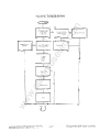
ATARI ®
VCS POP
ww
w.
FIELD S ER VICE MANUAL
m
m.
co
ata
rim
us
eu
AT AR I believes that the infor mat ion de scribe d in th is manual is accurate and reliable ,
and muc h care has been t aken in its preparation. Howeve r, no responsibility, financial
or otherw ise , shall be a c cepted for a ny consequences ar ising out cd the use of this
material. Informatio n contained here in is sub ject t o change. Revisions may be issued
t o advise of such changes and/or additions.
ww
w.
Correspondenc e regarding t his document should be for warded to Manager of Technical
Support, Consumer Product Serv ice, AT AR! , Incorporated, 845 Maude Avenue,
Sunnyvale , CA 94086.
ATA R! VC S POP Field Serv ice Manual
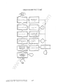
TABLE OF CONTENTS Title
Section
v
1
m
INTRODUCTIO N
THEORY OF OPER ATION
1-1
I-I
I-I
1-2
1-3
m.
co
Overv iew
Game Conso le
Ma in boa rd
Summary
SC HEM ATICS
(In pack et accompanying t his ma nual: •
3
TESTI NG AN D TROUBLES HOOTING
3-1
Equipmen t Requirements
Test
Static Mod ifications
Mod ifications Before Using The
2. 6 Diagnostic Cartr idge
Defective RAM Test
Co lor Bar Test
Gray Ba r Test
. Audio Tone Test
3-1
3- 1
3-1
? \
ata
rim
us
eu
2
DISASSEMBL Y FOR AD J USTMENTS
3-3
3-4
3-5
3-6
3-7
3A- I
Removing The Contro l Panel/Acc ess ing t he PCB
Changing Ga meplay Ti me
Setting Channel Po sition
DIAGNOSTIC FLOWCHARTS
11-1
Index of Flowcharts
4-2A
SYM PTO M CHECKLIST
5-1
Overvie w Controller Fa ilures Logic Failures Video Failures Color Failures Audio Failure s ROM Failures 5-1
5-2
5- 2
5-2
5-3
5- 3
5- 3
6
CON TROL PAN EL
6-1
7
PARTS LIST
7-I
8
SERVICE BU LLETINS
8-1
ww
w.
5
ATAR I VC S POP Field Service Manual
iii
*
3A- I
3A-2
3A-3
•
•
Changed per EC N !f0007 11 /19 /82
LIST OF ILLUSTRA nONS
Pag e
Tit le
[ -[
Functiona[ Block Diagram
3-[
3-2
3-3
3-4
3-5
3-6
3-7
3-8
3A-1
PO P Static Modification (Zener Diode)
Assemb[y Installat ion
Mask Placement
F [O Switch Legend
Defective RAM I/O Patterns
Co lor Bar Scree n
Gr a y Bar Screen
Audio Tone Screen
PC B Location of A7, A8 and Channel Select
6-1
6-2
Control Pane l Schematic
Harness Cable Schema tic
[ -[
3-2 3-2 3-3 3-4 3-5 3-6 3-7 3-8 3A-2 m.
co
us
eu
ata
rim
w.
ww
m
Figure
6-[ 6-2 m
INTRODUCTION
m.
co
The Point-of-Purcha se (POP) Field Service Manual is a re fe rence guide for you, t he
servic e technician.
The infor ma tio n pre sen t ed in th is manual, when used in
c on junct ion with AT ARI tr a ining enables you to repair and maintain the POP display.
This Fie ld Service Manual is organized in eight sections:
• Theory of Operation - Overview of how the POP display works.
us
eu
• Schema tic s - Electrical drawings and layouts fo r major components (in a
separate pac ke t accompanying this manua J).
• Testing and Troubleshooting - Overview of tests which assist in diagnosing
malfunctions.
• Diagnostic Flowcharts - Detailed procedures for troubleshootin g and
repairing the PO P display.
ata
rim
• Symptom Checklist - Failure informa tion t o assist the expe r ienced
technic ian arrive at a rapid diagnosis of problems.
• Cont r ol Panel - Sche ma t ics for troub leshooting failures with the control
lines.
• Parts List - Deta iled breakdown of all parts used in the POP disp lay.
ww
w.
• Service Bulletins - Section to be used to hold Field Change Order s,
Upgrade Bulletins and Tech Tips.
ata
rim
w.
ww
m
m.
co
us
eu
I
I
I
I
SECTION 1
m
THEORY OF OPERATION
m.
co
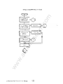
OVERVIEW
,
Select Switc hes
I
I
I/O
651 2 R.-.M- I/o Otio
ata
rim
;
-t-- - - - - - -~
Select
CirC\Jitry
f(OM
(Came ControUer)
Gall'll! ROMs
Power
Suool,
..
Video Converter
,,
I
I
I
Audio
Genera tor
I
I
~
.J
l-
I
RF Modulator
.::=J~
w.
Battery Elim in.JtOf
(AC Adap tor)
~
I
'I ..
Re5et
loOK
I
I
I
"1
J
,
I
1
Microproceuor
+
I
I
A- Io-O Converter
,,i~
"01
r emporary R....M
TI;O'-;----,
I
Control Panel
,,
r -- --- - -----'
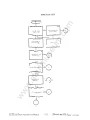
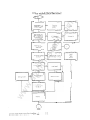
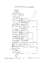
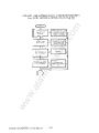
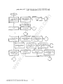
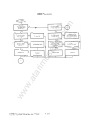
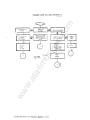
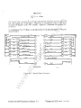
Figure 1-1. Fuctional Block Dia gr am
ww
L
J
I
I
I
5toraKe
r- --
r----'
Select Circuitry
I
I
I
us
eu
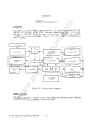
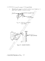
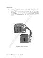
The POP is a state-o f-the-art microcomputer.
It rec eives instructions for the
opera tion of differen t ga mes fro m individual Read-Only-Me mory (R OM ) game
c artridges.
The POP in terprets data from the .;ame con t rolle rs and executes
comma nds on t he te levision screen. Figur e I-I is a bloc ". diagram of the functional
flo w of the PO P.
GAME CONSOLE
The POP board sets in a me tal enclosure tha t shie lds the mainboard fr om rad iating ·
e lectron ic noise which originates in the telev ision set.
AT ARI
ves
PO P Field Ser vice Manual
1-1
MAINBOARD
•
m.
co
m
Th e mainboar d is a Prin ted Circuit Board (PCB) wh ich holds th e po wer supply, the RF
modulator, the microprocessor (M P U) c hip, a combinat iu,' Random Access Memory
Input/Output (RAM-I/O) chip, and a Television Interface Adaptor (TIA) chip. The
board also includes numerous capacitors, resistors, tran3istors, and other assorted
electronic components.
Po wer Supply
•
RF Modulator
us
eu
The power supply is composed of a +5 vo lt regulator, filter capacitors, and
the power O N/OFF sw itch. Unr eg~ lated DC is supplied to the logic po rtion
of the PCB fr om t he AC power adaptor. A suppy of +5 is routed thro ugh a
filter circuit to the RF modulator.
Th is reduces the a mount of RF
radia tion generated by t he ga me.
The RF module converts the signal r e ceived from the Telev ision Interface
Adaptor to a frequency t hat a telev ison can r eceive and int erpret. A
coaxial cable passes this signal from the RF module to the c able mounted
t o the oack of the television.
•
Microprocesso r Chip
•
ata
rim
The 6507 Microprocessor (MPU) ch ip is an 8-bit microprocessor that is
re sponsible for the coordination of all circuitry in the POP . It c ontrols and
monitors t he functions of t he RAM and the TIA, reads informat ion from
the ROMs and instruc ts t he TIA in what to disp la y.
Random Access Me mory-Input/Output Chip
•
w.
Temporary storage of data from the MP U is prov ided by the 6532 Random
Access Memory-Input/Output (RAM - I!O) chip. This ch ip scans the I/O
joystick lines for input. It also kee ps track of the internal timing of the
chips for accurate video coordination.!
Television Interface Adaptor Chip
ww
This ATARI proprietary c hip genera tes audio and video signals which are
r equired by t he RF modulator. The TIA a lso contains the analog-to-digital
c onverter circuitry that allows the MPU to understand signals originating
in the paddle game controllers and to keep track of all player missiles a nd
c ollision registers.
The TIA outputs are proc essed by additional Circuitry in to a composite
v ideo, sound and color signal which is routed to the RF module. It also
generates the Sync signal for the unit.
•
Color Circu it
The master oscillator consists of a c rystal, t wo transistor s and additional
circuitry which oscillat e at a frequency of 3.57 MHz (plus or mi ,'us ,004).
ATARI VCS POP Field Se rvic e Manual
1-2
SUMMARY
m
The POP is a micc oco mp uter tha t enables the user to sele c t any o f the ATARI ROM
cartridges ins talled on the PCB and pla y it for a predetermined period of ti me.
ww
w.
ata
rim
us
eu
m.
co
Three c hips on the mainboard allow for the interaction bet ween the game and the
playe r. These chips are t he microprocessor (MPU), t he Random Access Me"mo ry
Input/Output (R AM-I/O) and the Television Interface Ada ptor (TIA).
A TARI YCS POP Fie ld Servic e Manual
1-3
ata
rim
w.
ww
m
m.
co
us
eu
SECTION 3 m
TESTING AND TROUBLESHOOTING m.
co
EQUIPMENT REQUIREMENTS
You require the follo wing six pieces of equipment before
y OU
c an troubleshout ·: hc
ATARI VCS T'vI Point of Purchase Disp lay unit (PO P):
15MHz Oscillo scope
•
Frequency Counter
•
2.6 Domestic Diagnostic Cartridge
•
Signal Tr ac ing Device Ch ip
•
Color Television Set (properly adjusted)
•
PO P Field Service Manual
us
eu
•
TEST ata
rim
Before you begin troubleshooting the POP you must make t he following modifications. I. The POP Ga;ne ROMs must be modified according t o POP ROM
Modification, page I (part nu mber FDI00029 ), regarding placement and /o;
replacement of Game RO Ms. This ensures t hat you are not repairing ,.
game RO M wh,ch is to be la ter re moved.
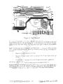
2. Install the static modification per the following instruct ions:
A. Make c er tain that you have t he following:
w.
I) Zener Diodes (lN37 47 - COl7654) two each.
2) Capacit ors (.0047uf - COI4180-08) two each.
ww
3) Masking compound.
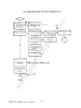
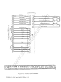
B. Attach the Zener Diode t o t he capacitor (See figure 3-U.
Make c e rtain that the polarity is correct.
C. Make certain the holes into wh ich the assembly (built in Figure 3 .1. )
. ·is to be inserted are clear of all solder .
D. Insert and solder t he two assemb lies (built in Figure 3- 1) into the two
locations indicated on the POP PCB (See Figure 3-2).
E. Coat the areas shaded on the top of the PCB (as illustrated in Figure
3-3) with masking compound.
ATAR I VCS POP field Service Manual
3- 1
Tne POP PCB is now statically modified to Atari specifications.
With the c ontro l panel o f t he PO P off, carefully clean and lubricate -::Oc
metal finge rs of eac h X-Y (joyst ick) controller.
m
3. m.
co
C 017654 _ _ !Io...~~~~~--C0 141&O-O& Cap
r...IIII<f-___-wrap Lead
I Turn &: Solder
ata
rim
us
eu
Figure 3-1. PO P Static Ivlodificat ion
(Zener Diode)
C
w.
7
4
Ha rness
.......! ---Edge Connector
ww
Figure 3-2. Assembly Inst allation
AT ARI VC S POP Field Servic e Man ual
3-2
~.
0
•
•
• •
•
-
m.
co
-
m
/Y: : ,.-
0
4
0
0
0
0
•
":=:::..
- -...:::
us
eu
---t-I ~I HImwII (ffIII
Figure 3-3. Mask Place ment
ata
rim
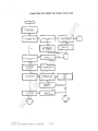
The test ing of t he PO P is in two parts. The first par t use s just the display s of the POP
it self t o de t e rm ine if it is in de e d defe ctive. If you determ ine tha t t he un it is indeed
defective , you must then use the 2. 6 Diagnostic cart ridge t o pinpo int the pr oba ble
error.
Before you c an use the 2.6 Diagnost ic c a rt r idge, however, you must modify the PO P
PCB. Per for m the following two instruction s before trying to use t he 2. 6 Diagnost ic
cartr id ge.
Re move the ROM in posit ion 7 (M6).
2. Re move t he t wo jumper wires at position FlO (to the right of the R F
jack).
w.
l. 3. Press position 4 on dev ice A8 to the ON position for infinit e ga me play.
ww
Th e 2.6 cart r idge can now be calle d to t he screen by you se lecting ga me 7.
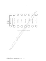
Because of t he physical a bsenc e of player option swi t c hes, you must short c e rt ain lines
t oge t her in order to get t he proper diagnostic disp layed on the television sc-eer,
These lines are loca t e d at F lO. Figure 3-4 illustrat es which lines must be shorted.
AT ARI VC S PO P Field Serv ic e Manual
3-3
Changed per ( CN 110007 11 / 19/82
m
>
.!::
::l
u
--i:3
;;::
..c
.....
0::
-l
.~
- - -"
0
IJ..
.~
i:3
....
m.
co
::l
~
~
Vl
a.
0
a.
u
Vl
--
-'"
U
cO
~
....
S
"
0
u
u
~
"
Vl
~
Vl
a'"
us
eu
>
.!::
000000 - '" "
'"
"'"
"
~
~
"
"
E
E
()
()
'"
'"
0 0 0 0 0 0
ww
w.
ata
rim
Figure 3-4. F lO Switch Legend
AT ARI yeS POP Field Service Manual
3-4
Defective RAM Test
Purpose : To test t he 6532 chip (RAM I/ O) for proper operatio n.
•
For mat:
m
•
At power -up, the television displays solid diagonal of some type
if the RA M is defec t ive .
Figur e 3-5 illustra tes some of t he known
w.
ata
rim
us
eu
m.
co
examples of screens which indicate a defective RAM I/O.
ww
/
Figure 3-5. Defective RAM I/O Pattem!.
AT ARI ves POP Field :,ervice Manual
3-5
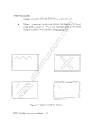
Color Bar Test
P urpose : To t est the c olor-generating functions of the TlA chip a nd
associated circuitry for proper operat ion.
•
Format : A screen of 15 horizontal color bars is displayed (See Figure 3
6).
The screen should be steady and unchanging.
A gray or blue
horizontal reference line extends across the screen about four bars from
the bottom. This reference line is thinner than the bars around it. R7 0
;hould be adjusted to t he bars immediately above and below the reference
line co within one shade of each other. (The bars should be goldenrod in
colo<.) Proper operation of the unit is indlcated .by being able to make
this adjustment and by consistent co lor within the entire span o f each bar
on the screen.
Minor glitches on the edges of the color bar are
acceptable. Leave this test on for at least 60 seconds in order t o catch
any intermittent pr oble ms, such as a bar momentarily changing colors or
b lank ing out.
us
eu
m.
co
m
•
***
NOTE
* ,. *
ww
w.
ata
rim
Figure 3-6 is a black and white re presentation of a color telev ision screen.
Figure 3-6. Co lor Bar Screen
BAR ;\ T ARJ VCS POP Field Service Manual
SAME COLOR
3-6
Geay Bar Test
Purpose: To test the fu nc tion of the lu minenscence lines (LMO, UvlI, and
LM2) from the TIA chip to t he RF module.
m
•
ww
w.
ata
rim
us
eu
m.
co
Format: Shor;_'_he color/black and white switch with t he proper tool.
Eight horizontal gray bar s are displayed, going from black at the cop t c
white at the bottom in even steps (See F,gure 3-7). The screen should be
steady and unchanging. The lines may have minor glitches on their edges.
A thin whit e line always appears just o" er t he top (black) bar. No color
should appear anywhere on the sc reen. T.e areas above the top (black)
bar and below the bo tto m (white) bar are 0 "1 ClO importance to t he test.
Th is test should be left on for at least 60 seconds to ensure that there is
no "flashing" of color or sh ifting of the gray bars.
Figure 3-7. Gray Bar Screen
AT ARI ves POP Field Service Manual
3-7
-\ udio Tone Test
To test the function of the audio t one genera tion ac e'
Purpose:
modulatio n circuitry.
•
Format: Short the right difficulty swit ches. This test disp la ys two
a lte rnating patterns on the screen (See Figure 3-8) while two alternating
tones are heard. The tones change in sync with the screen. Th is test
continues for one full cycle after the switch returne d to the initial
position.
ww
w.
ata
rim
us
eu
m.
co
m
•
Figure 3-8. Audio Tone Screen
AT ARI ves POP Field Service Manual
3-8
SECTION 3A
DI5A5SEMBL Y FOR A DJUST MENTS
REMOVING THE CONTROL PANEL/A CCESSING THE PCB
m
A. Unloc k the sliding doors.
m.
co
B. Remove doors• . Slide doors t o open position; lift each separa tel), and pull the bottom towards you. C. Re move the VCS security bar fr om t he top of t he control paneJ
D. Kemove all plugs from the VCS.
E. Remove the VCS from the c ontrol panel.
G. Remove the carriage bolts.
relieve t e nsion on the bolt s. us
eu
F. Remove the wing nuts fr om the carria ge bolts located at the Dac k of the contro l panel on the unders ide, about five inches from each sIde 'Jane l. You may have to lift the comeo l panel to H. Unp lug the c onnector halfway between t he blac k box and the coc,lro l pane l
ata
rim
I. Remove the t en Phill ips-head screws holding t he plexig lass cover on the contro l panel. J . Remove the menu c ard and discard.
K. Put the new menu c ard in place.
L. Cover t he card with t he plexiglass an d secure with the ten Phillips-head screws removed in Step l. M. Turn the contro l panel over . Be careful not to damage the joysticks.
o. Lift
w.
N. Snap the black bo;, connec t ion on the PC B c able together wiTh t he one on the control panel. Do not force this connect io n. If the connection cannot be eastiy made, check to make certain that the pins and pin connectors a re correctly aligned, and t ry again. In
place ww
and replace the c ontrol pane l. Make certain t hat t he PCB is
and that aJJ cabling is properly st ored. P . Insert carriage bolts, wh ich were removed in Step G.
Q. Secure carr iage bolts with wiring nuts.
R. Place dummy VCS in same location as the VCS re moved in Step E.
S. Secure IIC S with secur ity bar removed in Step C.
T. Replace sliding doors. Insert back door (without t he lock) top fir st, and t hen ger,tly push in t he botto m of the door. Use the same procedure with t he front door. 1\ TARI
VCS FOP Field Servic e Manual 3A-l Changed per ECN fl0007 11 /19/82
SE.TTING CHANNEL POSITION m
The PCB is set te op erate on Cha nne l 3 of your telev ision. If a loca l te lev ision
station is interfer ing with the game signal on Channel 3, you can c ha nge the ga me's
c hannel to Channel 2. If you wish to change chan nels, read on, if no t please push
t he PCB back into place and r everse the procedure s in the Remov ing the Contro l
Panel Section, page 3A-1.
m.
co
To chan~e the channel setting, you need t o cha nge the "jumper" t ha t is on the PCB
itse lf. If you have not already cut the olastic tie that ho lds the PCB in the the
metal box, cut it from the outside of the box a nd carefull y re move it.
ww
w.
ata
rim
us
eu
Now, pull the PC B towards you aDout 5 inches. The plugs are located beh ind t he
back-right corner of the RF module (silver-co lor box). Refer to Figure 3A-l on the
preceding page ••
ATARI VCS POP Field Servic e Manual
3A-3
Changed per EC N 110007 I l/19/82
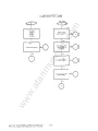
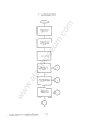
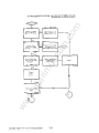
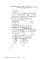
DIAGNOSTIC FLOWCHART
m
SECTION 4
m.
co
The Diagnostic Flow Chart is intended to be e asy to use and the pr imary aid when
trouble-shooting the POP. Follow the prompts in the order presented. When a
questio,., is asked, follow the line fro m t ha t box which best applies t o the unit's
situation. When that line terminat es with a le t ter inside a circle, turn to that page,
locate the letter in another circle, and continue t he diagnosis. The flow chart leaves
nothin g to chance, It t ells you when to perfor m a specific t est, and when t o replac e
co mponen ts.
us
eu
When t he flowchart branches to R - c all ATARI, Techline Specialist.
Inside California
(800) 672- 1466
Outside California
(800) 538-1535
ata
rim
CAU TiON:
Extreme care should be taken when handling t he in tegra ted circuit c hips. They are a ll
very sensitive to stat ic elect ricity and can easily be erased by careless handling.
Always keep the chips in the ir plastic carr ie r t ubes or on conductive foam when not
handlinlC them. Make certain you are well grounded when handling t he c hips. Atari
stronglY recommends that you wear a conductive grounding band (whic h ties from your
arm to ground) when handling the chips. The chips are also suscept ible to damage
from stress when being removed from or in serted into the sockets. Alw ays use a chip
puller when removing the chips. Do not pry the chips out with a screwdr iver or a ny
other tool.
ww
w.
Failure to follo w the above guide lines resu lts in unusually high chip failure rates and
extra expense.
ATARI VCS POP Field Service Manual
4-1
POP DIAGOSTIC FLOWCHARTS
r-__
~~-+~
N
~
O~
Ye '
Check for shorted m.
co
Old customer
complain o f snowy
screen?
m
Start
Is/are diodeb) shor ted ?
diode. CR I f._r'Q 1q ________________________________________-J
F
prop~ly,
Any modulation on screen. ata
rim
Ye,
us
eu
Connect umt
Does anyone of the display panerns appear? thr~
Ye,
Do all display patte rn s 2) '-.iPU
)) RAM
41 TtA
ww
w.
appear wlthm IYz minutes?
Swapout L) C6 (lC)
ATAR! VC S POP Field Se rvic e Ma nual
11-2
~o
Yes
Rep lace
INDEX OF FLOWCHARTS D
DI
E
EI
F
G
GI
G2
H
I
J
JJ
K
KI
M
N
o
01
P
Q
~
S
T
Tl
U
UI
U2
V
VI
W
WI
X
XI
ww
X2
Y
Z
AA
AD
AD I
AE
AEI
AE2
m
4-22 4-3 4-4 4-4 4-21 4-9 4-9 4-1 5 4-16 4-2 4-10 4-1 1 4-1 2 m.
co
C
us
eu
BI
B2
Sing le ROM Faulty
Game ROM Test
Game RO M Test (Cont.)
Game RO M Test (Cont.)
Defective RO M Troubleshoot in g
Sno wy Screen Troubleshoo t ing Procedures
Snowy Screen Troubleshooting Pr ocedures
So lid Colored Screen Troubleshooting
Solid Colored Screen Trouble shoo ting (Cont. )
POP Diagnostic Flowcharts
Color Troubleshooting
Color Troubleshooting (Cont.)
Color Troubleshooting (Con t.)
De fe ctive I/O Line Troub leshooting
Trigger Line Troubleshootin g
Paddle Line Troubleshooting
Game Will Not RESET Troub leshooting (Cont.)
Gray Bar Troubleshooting
Gray Bar Troubleshooting (Con t.)
2.6 Cartr idge Test
Color Bar Test
Defective Sw itch Troubleshooting
Defective Switch Troubleshooting (Con t.)
Gray Bar Test
Audio Test Procedure
ATA RI , Techline Specialist
One Row - One Section Faulty, A Group of 4 Chip s
Single Row Faulty, A Group of & Chips
Single Row Faulty (Cont.)
Single Column Faulty, Column I As Example
3ingle Column Faulty (Cont .)
Single Column Faulty (Cont. )
Entire ROM System Fau lty
Ent ire ROM System Faulty (Cont. )
Game Wi ll Not RESET Troubleshooting Procedures
Game Will Not RESET Troubleshoo ting (Cant.)
Game Does No t RESET on ATAR I Logo
Game Does Not RESET on ATARI Logo (Con t. )
Game Does Not RESET on ATARI Logo (Cont.)
Bad SY NC Troubleshooting
RESET Tr oubleshooting (Cont.)
RESET Problem
RESET Troubleshooting (Con t.)
RESET Troubleshooting (Con t. )
Tim er Failure
Timer Failure (Con t.)
Tim er Failure (Con t.)
ata
rim
A
B
PAGE NUMBER
TITLE
w.
LETTER
ATARI VCS POP Field Service Manual
4-2A
4-20
4-43 4-44 4- 33 4- 13 4-1 4 4-5 4- 6 4-17 4-1& 4-7 4-8 4-1 4-23 4-24 4-25 4-26 4-27 4-28 4-29 4- 30
4-31 4-32 4- 34 4-35 4-36 4-19 4- 40 4- 37 4-38 4-39 4-41 4-42 4-42 Changed per EC N 110007 11 /1'1/82
ata
rim
w.
ww
m
m.
co
us
eu
Is "Enter Game
in blue?
m.
co
m
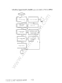
GAME ROM TEST No
Can you ad ;u5t R 70
N umb~"
so color is blue?
Cycle through a ll
Ad iust R70.
us
eu
ROM cartridg es.
ata
rim
Do the select &. reset
but tons work ?
Do all ROMS come up?
Is the audio unit
ww
w.
cOt'rect?
Y.,
Is the video correc t ?
AT ARI VCS POP Field Service Manual
11-3
Changed per ECN 11 0007 11/ 19/82
GAME ROM TEST (Cont)
m
~I
m.
co
S""&pQUt
00 the joysticks
function properly?
I) ROM
2) MPU
3) TIA
4) RAM
Ve.
Do the joystick fire
buttons function
Is video now correct?
us
eu
properly?
Ye.
ww
w.
ata
rim
Do the paddles
function propedy?
A TAR! ves POP Field Servic e Manual
1f-4
Yes
Do the paddle butto ns
function properly ?
Remove the two
jumper wires in
position FlO.
Remove ROM 117
&: inse rt 2.6 c art
us
eu
ridge in c artridge
socke t.
m.
co
m
2.6 CARTRIDGE TEST ata
rim
Select Game 117.
Does color bars pattt!m come up on screen.
No
Does gra y oan, matr' lX
ww
w.
or aud io pattern appear ?
ATARI yes POP f ield Ser vice Ma nual
No
Is S(re@fl either
solidly colored or
y~tically lined?
4-5
Reconnect POP
and initalize.
Ar e color bars present
us
eu
on screen?
m.
co
m
COLOR BAR TEST Yes
ata
rim
Adjust R70 50 color
is aligned prop@f'ly.
Is unit tunabJe to
ww
w.
prooer shades?
ATA R I
yes
pOP Field Service Manual
~-6
Short out color / btack
&: white switch.
Did screen pattern
change when switch
No
Color/black &
white line is bad.
us
eu
remo v~?
m.
co
m
GRAY BAR TEST ata
rim
Is proper gray bar
pattern present?
No
ls a partial segment
missmg or is !!!y
color present?
Ye,
ww
w.
Swapout
t) EF9 (TIAl
2) U'I19 (MPU)
3) J9 RAM
Proper gray bar
pattern.
A TAR! ves POP Field Se rv ice Manual
4-7
AUDIO TEST PROCEDURE
<:
~
.::>
m
I
I
Is there a dear tone ?
I Yes
Are the two panerns
1,'0
counter to measure
ro
us
eu
lYe,
Use scope or fr equency
fr equency at emitter
of Q8.
In
Ex. 3-7 alternating 00 the screen?
m.
co
Short ou t the Righ t DiU. SWITch PC. 00 tne pattern s
alternate with t he tones?
I
~
lYe,
Are both colors
and tones consistent
each cycle?
ata
rim
Tune Audio t o 4.;1 MHz
by adjust mg.
I
Adjust to ,:.06 MHz..
Look for stable fre quenc y.
lYe,
Remove Jumper.
I
Can unit be adjusted
ves WIU go through one Jast cycle before
and is sound clear?
changing to color bar
I
ww
....
Ye,
w.
J
No
Go to A udio TroubleshOO ting Procedu:l;,o. tC'st.
6
6
ATA R! YCS pOP Fie ld Se rvice Man ual
4-8
~'-
Swapout
\) El F9 TlA
Z) J9 MPU
J) L/M9 RAM
f-
A re patterns now
correc t ? (""5 In examp le)
0
fYe,
SNOWY SCREEN TROUBLESHOOTING PROCEDURES 0
::>
C
I
~
Is .'v present on
output of VR I?
7.5
DI
unr~.
on VR I
r-
F
~
Defective VR l.
I}r short outpu t VRI
m.
co
to ground.
INO
.. ' von Pin 4
RF module?
~
Rep lace RF nfodule
or bad RF cable.
r-
7. ' unreg. on J4?
Open between J4
and input "RI,
INO
INO
~
[s FM Ddec tive?
us
eu
th~ re
I
inpu t?
Iy"
Is
::>
DI
m
<
Replace FB4.
INO
Y.,
.5v snorted to ground ?
INo
Swap
Op~ be tw e~
I
I
Repa ir
w.
0
ata
rim
A20)
output and RF module
Pin 4.
t) T 1A
2l MPU
J) RAM
I
Any modulation ?
I ~o
ww
Defective J4 .
l
Repair
0
ATARI
ves
POP Field Ser v ice Manual
~-9
~
.
F
COLOR TROUBLESHOOTING
G
::>
m
<:
~
Ls an y color visable
(including refere nce
bar)?
INO
Is there a 2 , } to) ... p-p si~nal on a J 31\ volt level
betw~n
I~
us
eu
INO
the re a 4,5 ,,, p-p
on Pin 9 of TIA?
si~na l
Open between TIA
F
Pin 9 and C64.
ata
rim
INO
F-0 e6" and R71?
m.
co
I
No
Is R72 good?
IV.,
No
w.
Is R71 good?
ww
Iv.,
AT ARI
ves
Swrt°u t
1) T A
2) RA M
) MPU
I
POP Fie ld Se rv ic e Manu a l
Ii-L O
Re~;a c ::.
COLOR TROUBLESHOOTING (Cont)
C
GI
::>
...!!!..
INc
Does \/ Olt&1e vary
berween 0
6u on
Pin 10 of Tl A when
R 70 iJ rota ted?
~
INo
Defective
I) C6J
Z) TIA
-
Repair
m.
co
Is c olor constan t ly
roiling (cycling)?
m
I
[s YI frequ ency
) . 5n ' MHz.
~
Re p lace YI.
Y.,
us
eu
Swapout
1) TIA
Tur n R70 fully
clockwise.
2) MPU
)) RAM
lQ
I
I.s th~e 6" on anode
of CR t,?
~
DefKti ve R7 or open
between CR 2 - R7-U2.
-
ata
rim
I'0
' .,V on anode of
CR\4.
~
1'0
~
., on ca thode of
C R\4 .
w.
Defec t ive CRI4 .
lNO
ww
Ope n bet ween. 5 !t: CR 14. Replace
6
ATARI
ves
POF Fjeld Ser " ice Manual
4-11
Is R67 good ?
Y.,
Defl!Ctive CRI , .
~o
Repaar
0'
Replace.
"
C OLOR TROUBLESHOTING (Cont)
m
:>
G2
m.
co
<
Defecuve
YI
fr~ uenc y
J.57'n:!: .
~
1) Y I
21 Q'
Ve ,
-
~
tuned properly ?
I
Ve,
No
~o
Rep lace RF module.
ata
rim
R77 good.
Can RF module be
Ve'
C65 good.
-
No
Ve,
w.
RF cable good?
r-~
Replace.
ww
Veo
Replace RF modu le.
I
0
ATARI VCS POP Field Ser v ice Manual
F
us
eu
RF Frequency 61.25
MHz ".1 5?
-
4- 12
Repair
r-
Tune RF
I-
GRAY BAR TROUBLESHOOTING
c::
-,
K
m
I
m.
co
Short cokw /bw SWItCh
wltn apptoor..te item.
I
Is there a r..- ' v P'1l
ulM. lon leads 01 R7S
R19 and RIO on tM side
01 the nA?
~
KI
[No
.
ls tne!'e • Io_}v p-p
silnal on tn~ Tt A (EF,)
Pin for that line
us
eu
tn~ foUOWlII1 steps
~hl! line you ue to
look at IS the one tn. t
1ld no t ~v~ the atlOv~
For
SH
sIgnal.
I Yes
>Jpen tlet\\lee'n TtA
IEF9) and summU11
resuto r ( $fie eMu t).
l=hact.
11'0
ata
rim
RepLace TIA (EFI9)
I
Pus?
INo
ww
w.
Same 1ailure.
,,
,
TI" Pin ,
y"
F
r-o
Ty"
No
Checlc. puUUO reSIStors.
($fie cl\ar tl
I
?ullups good?
Iy"
Name
"L'
LI
?uUup Re sis tor '
Summ!tl\~:Si.stor ,
""
."
.&0
."
,\ T ARI ves PO P F ield Service Ma nual
""
1f-13
III qutKUOn II
shorted or ~.
L.in~
~
....
'
0
GRAY BA R TROUBLESHOOTING (Cont)
:::>
Kl
Swapout
l) TIA
2) MPU
3) RAM
I
Same Problem ?
~o
us
eu
IY.,
m
I
m.
co
<
Defective 1) R78. R79 or R80 2) RF module 01" shorted or open LM line. ata
rim
I
Repair.
I
ww
w.
G
ATARI ves POP Field Se rvic e Manua l
~- 1 4
SOLID COLORED SCREEN TROUBLESHOOTING <:
:::>
E
MHz
rG
EI
INO
Change
e•
IV
~
I) Y I
2) Q9
J) Other clock. component
or open between OK.. cIrCUit a nd TlA Pin 11 .
us
eu
[s there a 3 •.579 5 .I.-1H z
signal on Pin II o f T1A ?
m.
co
t. l~
Is the re a
signal on RAM Pin 39
m
I
Swapout
Is there
1. 19 MHz
oil
signal on pin II of
T1A
I) TIA
2) MPU or
Pin II of TlA
IS shorted.
ata
rim
Iyes
~
Is there
II.
1. 19
MHz signal on M PU
~
Pin 27
Open betw~ Pin II 01
TIA and pin 27 of MPU.
INO
Swapout
Is t here a 1.19 M Hz
si'Z,naJ on MPU p in 28
~
!) M PU
Z) TiA
J) RAM or
Pin 23 of 1o,\PU
1$
shOrted.
w.
lye.
ww
.Is 1.19 MHz
s ignal on TIA pin 26.
~
Open between TIA
Pin 26 MPU Pin 28
md RAM Pin )9.
-
Repair
-
I",
Open bet ween pin
39 of RAM and pin
23 of MPU.
I
ATAR I
ves
6
pOP Field Service Manu al
~-1 5
Changed per ECN fl 0007 II! 19/87
SOLID COLORED SCREEN TROUBLESHOOTING (Cent)
<
El
~
~
Open between Pin 26
TIA and Pin 39 RAM.
~
Open on line to eith@l"
m.
co
Is there a 1.1 9 MH~
signal on TIA Pin 26.
Iy';
and RAM
,
Iy·,
Are TIA, MPU, and
R AM ready and r e set
lines good?
~
Open or shorted line
or defC!Ctive n A
RAM or MPU.
f--
Repair
ata
rim
IY.,
. 5 or ground or deective MPU, n A or RAM
us
eu
13 there .. 5 and
ground on nA, MPU.
m
I
Swapout l ) MPU 2) RAM )) TIA I
Does ccx-rec: panern Y.,
w.
appear ? 0
ww
F
ATARI VCS POP Field Serv ice Manual
4-16
DEFECTIVE SWITCH TROUBLESHOOTING
0
::>
I
17
21
24
Lelt Ditt.
Co lor /B<!t. W
Game Reset
Game Select
POP l's Select
POP la's Select
in open position, is
t he re
C"
C88
C91
C90
23
POP Game Reset
With inoperative switch
"C84
It
~5v
present at t he A20 2 side of it ?
C36
C87
""
22
~
lYe,
~ wiTrh .
us
eu
t hp
.:..es cis
C"
C ln~~
[s switch
Internally
shorted'! m.
co
CAP /I
J9 Pin il--'
-6-
SWITCH
Right DilL
m
c
I
Swapout
Il J9
Z) LM/9
J) Ef/q Is (Iv now present ~
at the ram Pin fo r
that switch? c:r-
ata
rim
INO
Does switch now wor k ?
Is there aJl open
between A20 l and
that switch?
Ye'
-
I Yes
I
I{epalr trace.
ww
w.
I
ATARI
ves
0
POP F ield Service Manual
/;- 17
Is swi tc h connected
to
~round
on one s ide ?
I No
Iyes
Replace SWH(.:',.
DEFECTIVE SWITC H TROUBLES HOOTING (Cont)
Is cap on that line
short ed to ground?
~
No
b the re ·5v on the
RAM Pin for that
swhen?
~
Replace Cap.
Swapout
I) 39
2) LM/9
-
-
)) Ef/9
us
eu
(see chart).
Y.,
m
')
0'
m.
co
c:::
Open between RAM
ata
rim
Pin and ino perative
switch.
Repair
SWITCH
DiU. Ri~nt
l.eft DiU. Co lor/86cW
Game Reset Ga me Select
POP Ga me Reset
PO P I's Select
POP \O' s Se lect
ww
w.
F
AT ARI YCS POP Field Se r vice Manual
4-18
J'J
-,-. -C3-,,
" C8C3C98,
"2) C90
Pin /I
c.~p
ZI
'8
'9 22
C8.
CS7
C"
/I
BAD SYNC TROUBLESHOOTING
::>
y
I
~
<Channel 3)
Iv,,
Defec ti ve R8 l or
bad EF9?
~
Can RF
modu l~ be
proper ly tuned?
~
m.
co
RF module tuned to
61.2, MHz.?
m
c
ReDiae!! R F module
I
Yo,
J.!i-!iv P"1' signal on
A201 side of R81.
Tune RF module.
us
eu
J
No
Swapout
Ll EF9
Z) l.M9
3) J9
ata
rim
1
Yes
Good Video?
I
1'0
ww
w.
Defect ive R7 6.
I
Repair
I
6
ATARI VCS POP Fie ld Servic e Manua l
4- 19
Change d per EC N fl0007 11/19/82
m
DEFECTIVE I/O LINE TROUBLESHOOTING Det ermine which
Is there ..5v on the
J9 Pin fo r that tine.
m.
co
line{s) to look at
by consulting chart
below.
Close .:he c ircuit
(rnay!.! joystick).
No
us
eu
No
Unhook POP panel
[s ther e 0 ... on
from board.
that Pin?
Swapout
Yo.
11 J '
Is there ... 5'1 on the J9
Pin for that line ?
ata
rim
Defecnve panel;
tha t line is shorted.
2) L M9
3) EF9
No
Rep lace ]9
Is there .. jv on the J9
ww
w.
pin for tha t line.
ATARI
ves
No
Padd le
~
Jo:r: nick
Left
R igh ':
Left
Left
Let ·
Left
Right
Either $hon ed or open
trace on that line
o r shorted cap (see c hart)
POP Field Service Manual
4-20
Right
Right
Right
Direct ion
Up
Down
Left
Righ t
Up
Down
Left
Right
J'
Pin
..
-U
IJ
"
12
13
"
"
C ,
W.
C>7
06
C"
C62
C61
C60
O.
on~
ROM bad ?
,\10
[s thert! a one row/one
s~tion failure? (I!!x. C6.D6.F6,and FI) (4 chips) us
eu
No
m.
co
(s only
m
DEF ECTIVE ROM TROUBLESHOOTING (s there a single row
(8 chip ) fa ilure?
(ex; C6,D6,E6.F6.J6,
K6,L6,M6)
[s there a sin~Je column failure? 6J. ata
rim
(6 locations ex. Cl
No
is the I!!rotire ROM system faulty? No
Does the game
c or r~tly?
Does trill! ga me t ime
out c orrectly?
ww
w.
reset
ATARI VCS POP Fie ld Service Manual
4-21
SINGLE ROM FAULTY (ei ROM 1, DEVICE D6)
::>
A
Is the ROM correct?
-
No
m
I
Ins@rt the corr ect
ROM .
I Ye s
Is j um~ in p(ace?
-
Yes
Does 06 Pin 24
have .5V?
I
Put iu m p~ on
connector .
---
Troubleshoot RS4 (or opens and shor ts. ~
Is A6 Pin 16 h i ~h?
I
, . Yes
(06 )
Yes
~
Troubleshoot openl
shor t be tween A6
Pin 16 &: D6 Pins
ata
rim
Replace ROM I
2 0 ~21.
I
I
ww
w.
6
Pin 18?
Y ••
No
Ye.s
Are Pins 20 &: 21 on
0 6 h i~h?
Is a signal on
us
eu
I
No
-
m.
co
<
ATARI ves pOP Fie ld Service Manual
11-22
No
-
Repa ir
~
trace.
:>
5
I
~
Are Pins 1!3c 19
on H6 low ?
t
._
Troubleshoot for open I
shor t on data lines
between H6 &:: C6 •
us
eu
Yes
Are t here signa ls on
D XO - OX7
I No
openl
short Pin ( of M/1'I7
to Pins I&:: [9 of H6.
Yes
A re dat<'. sIgna ls
present on H6':
I
Troubleshoot for
m.
co
<
on H6 ?
~
Rep lace H6.
No
Troubleshoot data
lines H6 - K3 for opensl
shorts.
I Ye s
Are t here da ta siRnals
on Pins I }-1 7 on K8?
Yes
ata
rim
I
I--
ww
w.
0
A TARI VCS POP Field Serv ice Manual
m
ONE ROW - ONE SECTION FAULTY, A GROUP OF FOUR CHIPS
(i.e., ROW 0; SECTION X, DEVICES C6, 06, E6, &: FI)
4- 23
,
No
7V
C = .. IOV?
Are CRl1
CR 12, and R" the
right value?
Ye'
Does Q6
E. =..
,v
No
us
eu
No
1$ Pin 1 ot
.Y1/N7 low ?
Yo<
Tro ubl~ 5hoot
open!
short.
ata
rim
1 on NIP
and Pins I de: 19
on A6, B6. H6. 6c
N6 low?
Are Pins13-1.5
ot M/N7 low ?
Yo,
No
l; ~ in
Yo,
Do signals
A~AB8:::
No
Do ABO - ASll
at ~P U hav~
signals on them.
Yo,
Troubleshoot
aoen / short
ww
w.
AS I I
'6-A B0, AB 7
A TAR!
ves
Rep lace component.
Check for open/short .
Ye'
Troubleshoot open
along ... , une.
No
m.
co
Doe, Q6
s ~ ..
o DEVICES m
SINGLE ROW FAULTY, A GROUP OF 8 CHIPS (i. e ., ROW
C6, D6, E6, F6, J6, K6, L6 AND M6) POP Field Service Manual
4-24
Replace M/N7.
Are address signals at
outpu t of A6. 8 6, No
R@piace faulty Chip.
N/ P1? No Do COL 11- 3 input
= OUputs on A6? m.
co
«
w.
ata
rim
us
eu
Replace A6. ww
,\ T,\ RI YC:', POP FIeld Service Manual
1f-25
m
SINGLE ROW F AULTY (Cont)
SINGLE COLU MN FAULTY, COLUMN ONE (I) IS USED AS THE EXAMPLE <: :>
"
..::::..
I
I
Yes Are Pins 20 « 2 1
on D6 hi~h? Yes
No Are jumpers pro perly
set? N;-
~
affected chi.os..
Properly installed
jumpers.
ata
rim
~ Yes
Troubleshoot to r opens from Pin 16 on A6
Pins 20 « 21 on
us
eu
Iyes
-
Rep lace A 6.
tYes
Are Pin s 20 &: 21 on K6 high? ~
(s Pin 4 on A& high?
m.
co
Is Pin 16 on A6 high?
m
I
Replace D6 & KG .
ww
w.
6
A TARI yeS PO P field Servic e Manual
4-26
f-
Yeo
hi~h?
Troubleshoot C/ 07
Pin ( 2 &: A6 Pin 4
fo r short .
m.
co
Is Pin 12 on C/07
No
Yeo
Is Pin 13 on C/ 07 Low ?
Replace C/07.
No
Y.,
Y.,
Troubleshoot Pin 2
on C7 . Pin IJ on
C/07 for short.
Reolaee C7 .
ata
rim
Do Pins 13, \4 &: I'
on C7 c arry address
B &A?
us
eu
No
Is Pin 2 on C7 \Ollo' ?
m
SINGLE COLU MN FAULTY (Cont)
No
DoPins,&6on
H3 have the same
signal ('-high &:
6- lo w)?
Y.,
Troubleshoot fo r open.
No
Does H8
ROMLATCH have
ww
w.
input pulse?
ATARI
ves
POP Field Servic e Manual
'1-27
Reoair
SINGLE C OLUMN FAULTY (Cont)
Does
m
U2
GOI«5Me have
m.
co
input pulses whlffi STAR T is pressed? Yeo
Ar e inp\,It signals on
Pins 4 « 7 of H8 high
and low
Ye '
Rep lace H&.
r e$ ~eclLve ly?
us
eu
Ye'
Check for
Are PIns 2 &: 4 on J8
h igh <l: low respeCti'lely? No
ope~.
00 08r. &: OBI of J8 ma te"': Pbs 2 Jt: 4? ata
rim
No r-~-----------------------J
ww
w.
Repair
ATAR I YCS POP Field Service Manual
1+-28
Does 2600A
porT.illn
m
ENTIRE ROM SYSTEM FA,U L TY No
m.
co
fu nction proper ly?
Yes
Ar e sLg nals presen t on J8 OB0-0S P Yes
Is there an output
Yes
Trouble shoot between
Is output signal on
H8101lo' ?
H 8 and J8 for open
or short.
No
No
Is there a short/open ata
rim
signal Dresen ( on
between HS Pin 1 1 Pi n ~ . of H&?
a nd C8 Pin 6? Ye s
Yes
ls a GORO"M0
Signal presen "( on Pin 1 of H8? (low when RESET
i.'5 p ressed) Repair trace NO ~==~
Is there a short/open ww
w.
between H8 Pin L
and MPU?
ATARI
Re place J8.
signal on J8? Ye s
Is a ROM LATtH
No
No us
eu
Ar e data input Signals
on HR.
vespop Field Service Manual
4-29
ENTIRE ROM SYSTEM FAULTY (Cont>
<
::> VI
I
MIN 7?
Pin I = low
Troubleshoot for openl
short between Ha, Pins
12. ". 16 &: M/N7 Pins
13 - l .s.
No
Troubleshoo t fo r open!
short between H8 Pins
5-6 de e7 , Pins 14- 15.
:=
t-
high
Yes
Are output signals for
C7?
No
~ short between C 7 &: C / 07
Pin 1 :: low Pins 2-4 = high I
Troubleshoo t for open/ us
eu
I
No
Yes
Are output signals for
Pins 2-6
-
m.
co
Are input signals lor
\1/N 7 Pins 13 - U low ?
m
I
Yes
No
Are input signals for
Troubleshoot fo r openl
~ shor t bet ween C7 &: C / 07 C/O]?
Pin I :: low P ins ), li, &: 13 ::z high ata
rim
I
t-
Yes
Are o utput signa ls for
C/D7?
~
Pin 2 :: high Pin s 4, la, &. 12:: low 6
ww
w.
0
Replace C/O?
ATA RI yes po p Field Se rvice Manual
Ii-3~
Repair
6
No Yf!S
pube at 08, Pin 10
when game is selected?
R~lac e
Is there a short /oo~
betw een 08 Pin Ii) &: J9 Pin 24 . No
pulse
\1 ult iple pulses.
Ves
Is the re a single (low)
pulse at F8 Pin II when
~ame
;'\10
starts?
Is th ~e a single (low)
pulse at E8 Pin 8 when game stars?
Yes
:-.10
Tro ubleshoot open/short
be twen E8 P in 8 &. Fa
Pin I I.
No
Is there a sing le (low)
puise at ES Pin 9 whe n game starts. Rep lace F8
ww
ATARI y eS POP Field Service Manual
[s t here a single (low)
pulse at DIES Pin 8 when
game starn.
v.,
Ve s
w.
Is there single (high)
pulse on Pin [0 on FS
when ~ame starts.
Is there a sing le (Jaw)
pulse at E8 Pin 10 when
game starts?
Ves
ata
rim
Y es
us
eu
;'\10
J9 m.
co
Is there a sing le Oow)
m
GAME WILL NOT RESET TROUBLESHOOTING PROCEDURES If-3 1
Replace Ell
Troubleshoot {or open
beNfeen DI ES P in 8 and
£8 Pin 9.
GAME WILL NOT RESET TROUBLESHOOTING (Cont;
Is there a single ( hi~ h)
p u~ on Pin '1 of 08
when game starts?
No
r--
m
:>
WI
Troubleshoot open/shOf"t '>etween 08 Pin 9 and F8 Pin [D.
Ye,
No
-
,~o
15 Pin 8 of D8 low ?
Is Pin 9 of C /08 high?
'--
Ve,
Yes
No
-
Troub leshoot open / shOf t
or wron!i1; nJue.
Replace C,' D8.
us
eu
[s Pin 8 ot C/ Dg low?
m.
co
<
Ye,
Troubleshoot openishOl"t
betw ~ ClOg Pin 8 and
08 Pin 8.
ata
rim
Repair
i5 there is a sing le
(low) pube on 0 8 Pin LO
at game start.
No
Ye,
w.
Replace 08.
ww
0
ATA RI ves POP Field Service Manual
/;-32
I-
R.epa ir
6
15 P n
1J
;>
<;I of.
:'8 ·ow?
y"
r-
Rep lace Eg.
' 0
Ye' Is there an ope n/ short
b etw~n
f3 Pin
Pin 8?
<;I
6: DIE S
r-
Repair trace.
-0
' 0
DI ES Pin 10?
Is ther e a hig h on
o/E8 P in lJ?
I
"0
Ye s
~
Is there a short/open ~
betwet!n D/E8 Pin 13 and C/D7 Pin 6? y"
-
No
If there are pu lses In
but no pulses out, r eplace CIOS. ata
rim
A r e. ':here pulse ( mput '
outp ut) on C, 0 8?
Trouble snoot for open be tween C/O! Pin 6. and D/ E8 Pin , ) . Repair
ww
w.
6
ATAR I
ves
PO P F ie ld Se rvice Manual
I
Yes
[s Pin} o f C / D7
low?
No
is ther e a low on D/ E.7
Pin <;I when game is
L
aeolace C /07.
os
Repair
J.ep lace DI ES
.
us
eu
~
Is ther e a pulse on
m.
co
<
m
GAME WILL NOT RESET TROUBLESHOOTING PROCEDURES (Conti
4- 33
selecte d.
I
Ye s
Trouble shoot for open
be tween C/07 Pin 5
D/E7 Pin 9.
I
Repair
fO
X
GAME DOES NOT RESET ON ATARI LOGO T
:::>
Is there a lo w on Pins I "0
Tro ubleshoot R56, R61
~ R62 for short /open.
~
Rep lace D/El .
) - , of E7 when a bu tton is pressed?
I
Yes
Is t here a pulse on E7
when an y button is
Iyes
us
eu
pressed ?
Is t here a pulse on
DIE? Pin 10?
I
Yes
I, Pin 9 on D/ El • Low at powet' -tJp ?
•
~
High when either
ata
rim
select bunon is ?
• Low when start is
Troubleshoot open
between E7 Pin (, d:
DIEl Pin to.
A
Is Pin 13 on DIE? high?
IYes
pres~?
I
Replace E7
Yes
ww
w.
If Pin 11 on D/ El (TIMER) is not low - replace DIE? ATARI yeS POP Field Service Manual
m
x
m.
co
<:::
0
-0
r0
Xl RESET PROBLEM
::>
AA
T
Are there pulses
No
Ar e there
on 03 Pin 6?
on D/E7 Pins 5 &: 6?
INo
Yes
Are there pulses
on 0 8 Pin 47
~
Replace 08
...
Are t here pulses
on D/E7 Pin 2
I
1ves
~
Is there "}v on 0 / E7
Pins I &: 4, and
a SYN pulse on D/E7 Troubleshoo t open
~
Troub leshoo t for
open be t w~n D/E7
Pin 2 and F7 Pin I)?
Yes
us
eu
Are the r e pulses
on 08 Pin )?
Fe
AD
m.
co
I
pul ~s
m
~
~
Troubleshoot open
Pin J? -rYeS
w.
ww
ATARI
ves
POP Fie ld Ser v ic e Manual
Yes
Replace D/ E7
Replace
03
0
I
ata
rim
R~ lac e
I
1+-37
Replace
...
GAME DOES NOT RES:::T
<
. )~.!
ATA RI LOGO (Cont)
::>
Xl
~
Troubleshoot
open/short.
~
Replace F8..
IYes
Is F8 Pin 12 high?
I
Yes
Are there pulses on
DIES Pin 4?
on
us
eu
pu~s
D/ El Pin 9.
~
IVes
Are t here pulses on
f 7 Pins I, 6, 7, 9, &: L5.
Replace
D/ E1.
&:
01 E:7 Pin 9. Yes
Ar e then! pulses or:.
F7Pin IJ?
I No
Replace F7.
Iyes
Are t here pulses on
OS Pin 57
No
~
Troubleshoo t open
0 8 Pin 5 &. f7
tletw~n
Pin 13.
8
ww
w.
AA
AT ARI
ves
~
Troubleshoo t open / ~ short
b etw~n F7 Pin I ata
rim
I
K)
~ Troubleshoot open /short.
IYes
Are there
m.
co
Is F8 Pin 13 low ?
m
I
pOP Field Service
~ianual
4-36
K)
-
Repair
6
GAME DOES NOT RESET ON ATARI LOGO (Cont)
c
XI
m
r
I
Set oscillo$Copt'..
.,
Are t here pulses on
Pin 97 Fa ~
Are there pulses on
Pin 6?
e8 ~
IYes Are pulses irlverted on FS
Pin &?
~
Ye'
Are same pulse
on E7
, No
Replace
Ye,
Replace e3
0
Fa.
o~ / sh or t. Troub leshoot
ata
rim
) re~ent
Are t here pulses on C3
Pins I. 2, "' , or n
us
eu
Troubleshoot open/
short betw~n ex
Pin 6 oS!: F8 Pin 9.
Ye ,
m.
co
AC .5MV ·'5MSEC.
Pins I &:27 Ye s
I. ' here data signal
on 2-7 Pin 13?
Yes I--
[5 t here data signal
on L/ M9 Pin IS? 2:!2..
Swa pout
I ) J9
Z) LM9 } ) EF9 I
Ye s
",0
Troubleshoot
w.
o p~ / shor t.
b E7 Pi., 12 low?
~
Replace f7 .
ww
d5
F
X2
"-TAR! yeS POP Fie ld Service IAanual
4-35
f()
RESET TROUBLESHOOTING (Cant)
:::>
ADI
I
Pin 4?
~
I
Ye5
Is there a pulse on
L/M9 Pin 1.
~
i
Yes
Swapout
I) EF9
2) LM9
3) :1 9
us
eu
TroUblesnoot
short open
Replace F8
ww
w.
ata
rim
6
ATARI ves pOP Field Serv ice Manual
11-39
to-
m.
co
Is pulse inverted on F8
m
c::::
...
'D
::::> Is there an open
be,tween DIEl Pin '
and 0 8 Pin 61
No
f
Are there pulses on
E7 Pins 9« 10?
IYes
Y.,
Rep lace f 7 .
•
is E7 Pin II
o Low = ga m4! on?
No
~
Y.,
Are there pulses on
1:.7 Pin 8 when Osc is on'? ~
Y.,
...i:2.
Rep lace E7
--0
~
Troubleshoo t open/or wrong value for R6 /j. -R 66. ata
rim
Is t here a small pulse
on base of Q7 with
OSC on?
Troubleshoo t opl!:n.
Troubleshoo t open.
us
eu
oPulse " Osc on'?
~
m.
co
<
m
RESET TRO UBLESHOOTING (Cant)
Y.,
Are there large
I
~o
Replace Q7 .
RESET pulses on
Q7 (co lle c tor)?
Y.,
A re same pulses on'
CIos Pin I t?
~
Troubleshoot shor tl
open.
I No
Replace C /O!. I "0
Tr oubleshoot open.
--0
w.
Y.,
A rc pulses inverted on
CIOS Pin 10? K)
ww
Y.,
Is there a pulse
Oow durin~ ga~ ) on
F& Pin 3?
6
e
ADI
A TA RI yeS POP Field Serv ic e Manual
Repair
1>-38
RESET TROUBLESHOOTING (Cont)
::>
l
I
I
Swap
No
L /M9
I
Yes
y••
Troubleshoot tor open between C8 Pins I &: I/. and L/ M9. No
Is there signal on
C/07 Pin 9?
I
~
Yes
Is there a.n inverted
signal on C/07 Pin 8?
~
Iy··
Troubleshoot for open.
Rep lace C/07.
K)
,
ata
rim
y••
Troub leshoot fo r open
between C / 0 7 Pin 8 a/'Id
C& Pin 2.
I
K)
us
eu
I
J9
EiF9
m.
co
Ar e there pulses on
L/M9 Pins 16, 17 , 26
~ 277
m
<:
No
Is there signal on
C/OS Pin 3?
~
Troubleshoot for open
betw~n CIOS Pin 3
and LlM 9.
IYes
Is signal inverted on
I
No
e / os Pin 47 Replace C/OS.
w.
I y.,
K)
Repair
Troubleshoot fo r
ww
open between C l Og
P in 4 and C8 P in ) .
ATARI
ves
POP Field Service Manual
C5
It-ltO
m
TIMER FAILURE Timer staru when
starts.
Are 88, 0 1, & 02
initialized and COunting pulses? m.
co
~ame
No
Whe n game is on
i.s Ba Pin t l low?
us
eu
Ye,
Is there switc~
No
ata
rim
continuity on A8?
Ye,
Are there TiMER
sIgnals between
ww
w.
A8 and TIMER and
Ol E7 Pin 11 and
TIMER?
ATARI ves POP Field
Se r ,,~ce
Manual
ii-iii
<
AEI
/'\n!'
th~re
::> I
-
Yes
Replace SICa
I
No
Is there an o pen
be tween sa &- B/C3? Yes Dur ing a garM
is B/C 8 Pin
11 low?
I
Yes
Are there pulses
-No
IYes
~~oubleshoot
;.;pen between
Troubleshoot tor open
on SYN pulse Leading
to ElF9.
l ~o
:~ ~p l.:l c:e
;': /C3
ww
w.
0
ATARI
ves
POP Fie ld Serv ice Manual
for
a/CS
Repa ir
Pin II and O/E7 Pin 'J
ata
rim
o n SiCa P in IO ?
us
eu
I
I Na
r-
m.
co
pulses
on B8 Pin 10?
AE2
(Cont)
m
TIMER FAILURE
4-42
-
Reoair
6
' - -_ - - , ._ _....1
Is t he re
Ov on
E/ F9 pin?
(S~
Ch a rt)
Is there .. , ... on
(See chard
No
E/F9 pin?
Def~ti ...e E/ F9 0.
open be tween E/ F9
&. nOl or defective
panel.
No
~
Unplug :on trol pane l.
Is there .. ' v on E/ F9
pin? (See chard
Yes
~
Defective
con trol
pane l.
No
e t ectJVI!
II El F.
us
eu
Swapout
I ) E/ F9
2) R93 or R94
3)
o r C9 3 o r
en
2) J9
tri gg~ line
shorted to r ound.
3) L/M9
E/F9 Pin
3l
Right Triggf"
36
0'
w.
ATARI ves POP held Service Manual
Repair
Replace
ata
rim
Left Trigger
ww
•
Y.,
~
m.
co
Press &. hold fire
butten.
m
TRIGGER LINE TROUBL.ESHooTING
4-43
Repair
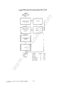
PADDLE LINE TROUBLESHOOTING m
C__J_=> I. cannot~e
used to
m.
co
Because of the absence of 9 pin connectors, the diagnostic cartridge
troubleshoot the POP. The steps to do so ar e:
Ensure that t he control panel is good by:
a. Measur ing the pot with an OHM meter , it should read O ~ with the
pot in one direction and IM~with the pot in the other direction.
b. Ensure t he lines are co mplete by ohming:hem out .
Ensure that the pot line on the board between E/F9 and J l is comp lete bv
ohming it out. (See char t)
3. Swapout the component on that part icular lin". (See chart, left to right.)
us
eu
2. Swapout Co mponents
f../F9 Pin
39
112
E/ F9
C 83
L
E/ F9
C82
ww
ATAR! YCS POP Field Serv ice Manua l
Itl
9
w.
Right Paddle
1+0
ata
rim
Left Paddle
Jl Pin
1+-1+1+
SECTION 5
m
SYMPTOM CHECKLIST
have been divided into six general categories of failure :
•
Controller
•
Logic
•
•
•
•
Video
Color
Audio
Failure~
ata
rim
ROM
us
eu
~ymptoms
m.
co
1 he Symptom Cnecklist IS designed to assist the experienced technician arrive at a
raoid diagnosis for POP problems. The c hecklist is not intended to replace the
Diagnostic Flowchart as the primary trouble- shooting guide, but rather , to supplement
t he f1owcha, t.
ww
w.
Each symptom is accompanied by some possible c auses and the best point to enter the
Diagnostic Flowc hart to locate the problem.
ATARI VCS POP Field Service Manual
5- 1
m.
co
CONTROLLER FAILU RES
m
SYMPTOM CHEC KLIST
Flowchart
Entry Point
Possible Cause
Trigger Line :
do not function
E/ F9, C 92 ,C9 3, Harness
Control Pane l
I, Pg. 4-4 3
Paddle Lines
do not function
E/ F9,C80-C83,
Harness, Control Panel
J, P g. 1+-41+
I/O (Joysticl<) Lines
do not function 0[
Paddle fire buttons do
not work.
J9 ,C55-C6Z , Harness,
Contr ol Panel
H, Pg. 4- Z0
us
eu
Symptom
ata
rim
LOGIC FAILURES
E/F9,J9,L /M9 ,Q9
YI, open or shorted
address or data line s
E, Pg. 4-15
Vert ically L,ned Screen
E/ F9,J9 ,L/M 9, open or
shorted address or data
lines.
E, Pg. 4- 15
w.
Solid Colored Screen
ww
Snowy Screen
VIDEO FAILURES
RF modu le, VRI, J'I
CR I 6- CR I 9
Wea k Picture
RF module RF cable
Wrong Gr af Bars
E/F9, R73-R75
." 'TAR!
ves
POP Fie ld Sen'ice Man ual
5-2
D, Pg. 4-9
K, Pg. 1+-13
m.
co
COLOR F AlLURES
m
SYMPTOM C HECKLIST (CONT)
Flowchart
Possible Cause
Entry Point
No Color at all
Yl , E/F9
G, Pg. 4- l 0
Only t he reference
bar appe ars
R70, Crl4 ,CRI5 Color will not adjust
Weak color
us
eu
Symptom
G, Pg. 4-l 0
R70 ,E/F9 ,C63 G, Pg. 4-l0
C64, C65,R77 G, Pg. 4-10
No Audio
Weak Audio
ata
rim
AUDIO F AILURES
C68 ,C71,Q8,L2 Adjustment
Q, Pg. 4-8
C68,C7l,C66
Q, Pg. 4-8
ROM F AILURES
ww
w.
Because of the complexity of the ROM circuitry there is no sympto m checklist for chis
fa.Jure. Instead proceed to the flowchart on Page 4-3.
ATAR I VCS POP Field Serv ice Manual
5-3
ata
rim
w.
ww
m
m.
co
us
eu
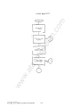
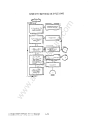
SECTION 6
CONTROL PANEL
m.
co
m
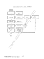
Tt">e Control f'and c onsists of a le ft and right joystick with fire buttons, and a left
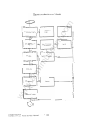
. and right paddle with fire buttons. Figure 6-1 is a schematic of the control panel includ ing the SELECT and STA RT button s. Figure 6- 2 illustrates the harness cable sc hematic. To troubleshoot the POP Panel dete r mine which line is bad and replace the suspect de fect ive parts. Black/White Stripe
Up
0
0
0
White / Red Stripe
(2)
us
eu
r-o
~
White / Bro wn Strip
HJ
Down
-0
-0
Left
0
White /Oranse Stripe
Right
0
White /Yellow StriP
()
Paddle
0
Orange/Wh ite Strloe
0
-0
Joyst ick
0
White / 8loe Str ipe
0
ata
rim
~
________________
14
0
0
~
f ~~I~'
__________
Green
~
f.:\
L..---......;;;..;;.;;;;,.-----...\!!I
f."':'\
White
I!V......
-;;,;;,;;;:-----I
CONTROLl. ERS
ww
w.
Figure 6-1. Control Panel Sc hematic .
ATARI YCS POP Field Servic e Manual 6-1
Changed per EC N 110007 11/[9 /8 2
•
j----- --- , White /Oranli;e Strip
,
OJ
~
::>
•
u.. 0
E
Black/White Stripe
0
0
Browf\
- e
0
Oran~e
9
~
8
Red
.",
OJ
::>
.S
0
~
U g
>-• Yellow
"
@
5
0.
@
Blue
@
Black
e
White
(0
Purple
17
Gr een
p
0
ww
w.
@
J
ata
rim
15
•
0.
0
,...
K
13 e
@
0
\Vhite/Purple Stripe I O's Select
~i
@
6
.:0< •'c"
....C
0
Whit e/ Blue Stripe
White / Green Str ipe I's Select
us
eu
'"
G
(0 @
White /Yellow Strip
0
0
A
@
White /Red Str ip
0
Gray-Grou nd
G
m.
co
0
0
m
White /O ran~e Strip
Figure 6-2. Harness Cable Schematic
AT ARI VCS PO P Field Service Manual 6-2
White/ Black Str ipe - Start
Gray - Ground
0
0
0
~
SECTION 7
~
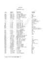
Part No.
Description
Main
Main
Main
Main
Main
Main
Main
0377 52-01
122012-103
128002-151
136003-101 ·
137149-001
137176-001
PC Board (POP)
Cap. Elec 10000 UF (L6 V)
Cap. Mica 150PF (50 V)
Cap. Mica ~7P F (L OOV)
Pr og RO M 0 (L 3700 1-00 1)
IC 74LSli
IC 7~C2 1+ 1+
Main
14-5102
Resistor Ii. W 1K
Main
Main
Main
Main
Main
Main
Main
14-5103
14-5153
14-5151+
14-5183
14-5221
14-5273
14-5332
Resistor
Resistor
Resistor
Resisto r
Resistor
Resistor
Resistor
Main
14-5391
14-5471
14-5472
14-5563
14-5821
[,, -5912
179048-002
179049-002
19-411504
20670-01
Resl:.tor Ii. W 390 Oh m
Resistor Ii. W ~ 7 0 Ohm
Resistor Ii. W ~ .7K
Resistor Ii. W 56 K
Resistor Yo W 820 Ohm
Resistor Y. W 9.1 K
Square Ter minal 2 position
Mini Jumper 2 position
Resistor Variable 500K
Test Points
Cap. Mylar .~ 7UF (L OOV)
Cap. Elec 2.2U F (50 V)
Cap. Elec ~.7UF (50V)
Diode IN 100
Diode lN5401
Diode IN914
Transistor 2N3906
Transistor 2N356 3
Transistor 2N3643
Transistor 2N6044 (T0220)
IC 4040B
IC 4584B
IC 7406
IC 74LS166
IC 74LS273
IC 74LS367
Regulator LM323K
2~-500~75
31-IN100
31-IN5401
31 1N914
33-2N3906
34-2N3563
34-2N3643
34- 2N6044
37-4040
37-4584B
37 7406
37 - 74LS166
37-74LS273
37 74LS367
37-LM323K
m.
co
us
eu
Y. W 15K
Ii. W 150K
Ii. W 18 K
Ii. W 220 Ohm
Ii. W 27K
Ii. W 3.3K
ata
rim
2 1- 10147~
24-500225
ww
Main
Main
Main
Main
Ma in
Main
Main
Main
Main
Main
Main
Main
Main
Main
Main
Main
Main
Main
Main
Main
Main
Main
Main
Main
Main
Locator
Ii. W 10K
w.
Main
128002-~70
AT ,>"RI VCS POP Field Service Manual 7-1
m
POP PARTS LIST
C7 ~
C9 ~
C6~ , 67 ,70
C6
E7
AI-6,BI -6,HI
6,K8,L8,NI-6
R 1,16,25,34,43,51,5; ;
61+-66 ,71,72 ,82,35
R91 ,9 2
R79,81,86,95
R87
R83
R93, 94
R68 ,80,8 9
R2-15, 17 -2~,26-33,3 5-42
44- 50,52,5~ ,56-63 ,69,73 -77
R88
R53
R67, 90
R78
R96
R81+
R7 0
C7 6
Cl, 12,19,26,33,4U
C72 ,97
CR13
CR 16-19
CR l -1 2,14,15,20
Q9
Q8
Q7
Ql -6
B8,B/C8
C/D8
N/P7
F7
H8
B7
VRI
Locator
Part No. Description
Main
Ma in
Main
Main
Main
Main
Main
Main
Main
Main
52-008 66-11 4PlT 72-1404C 72-1608C 72-1808C
75-0 18C
75-9951 4
75-995 16
75- 99 518
78- 06001 78 - 22 119 Jumper
DIP Sw itch (4 posit ion)
Screw Philips 114 40 X M. LG
Screw Philips 1t6 32 X Y2 LG
Screw Ph ilips 1t8 32 X y, LG
Washer Flat 1t8
Nut Washer Assy It4-40
Nut Washer Assy 116- 32
Nut Washer Assy It s 32
Heatsink
Cable C lamp
Tie Wrap
Conne ctor Phono Ja ck
IC TIA
IC C04050B
Cap. Poly 820PF (50 V)
Inductor Var iable 12 li2 turns
Prog ROM II COMBAT
(C X26 0 l)
Prog ROM 2 AIR- SEA BA TTLE
(C X2602)
R
Prog ROM 22 OUTLAW
(C X2 605)
Prog ROM 25 SLOT RACERS
(CX2606)
Prog ROM 8 CANYON BOMBER R
(CX2607)
Prog ROM 27 STR EET RACER
(CX2612)
Prog ROM 2930 TIC-TAC-TOE
(C X2618)
Prog RO M 32 VIDEO OLYM PICS
(C X2621)
R
Prog ROM 7 BR EAKOU T
(CX2622)
PROG ROM 16 HOMERUN
(CX2623)
Prog RO M 5 BASK ETBALL
(C X2624)
Prog RO M 13 FOOTBALL
(CX2625)
Pr og RO M 17 H. CANN ONBALL
(CX2627)
Prog ROM 6 BOWLI NG
(C X2628)
R
Prog ROM 24 SKYDIVER
(CX2629)
78 -24010 Main
CO l 1202A
Main
COl 1205
Main
COl1206
Main
COl 120 7
Main
CO l 1212
Main
C01l218
ata
rim
COll 221
C01l222
ww
Main
™
™
™
w.
Main
79-5903 COI0444 COI0816 COI0821 CO I0823 C01l201
us
eu
Main
Main
Main
Main
Main
Ma in
Main
Ma in
COl1 223
Main
<;011224
Main
COl1225
Main
COl1227
Main
COl122 8
Main
CO l 1229 A7,A8
m.
co
Assy.
Mail'
m
POP PARTS LIST (Continued)
ATARI VCS POP Field Service Manual 7-2
™
™
VR I
J6
E/F 9
J8
C 68,71
L2
F5
E6
L4
03
C5
F3
K3
C2
M6
C4
K6
K5
04
L6
C3
m
POP PARTS LIST (Continued)
Part No.
Description Main
COl1 233 Ma in
C01l 2311
Main
COl1239
Main
C0 1200&
Main
C012009
Main
C01 2010
Main
CO l 201 3
Main
C01 201 5
Main
C 01201 6
Ma in
C0120 1?
Main
C01 20 30 Main
C 0 1203 1B Ma in
C0120 32
Main
C012035
Main
COl2036
Prog RO M 20 NIGHT DRIVER R
(CX26 33)
Prog ROM 111 GOLF
(CX26 311)
Pr og ROM 21 OTHELLO 1
(CX2639)
Prog RO M III SU PE R BREAK OU T R
(CX260&)
Prog ROM 3& DEFENDER 2
(C X2609)
Prog ROM 311 WAR LOR DS
(CX26 10)
Prog RO M 1 ADV ENTURE
(C X2613)
Prog ROM 112 DEMON/
DI AMO ND (C X2615) TM
Prog RO M 23 SOCCER
(C X2 616) Prog RO M II BAC KG AMMON
(C X26 1?) Prog RO M 10 C IRCUS AT ARIR
(CX2630)
3
Prog RO M 28 SU P ERMAN
(CX263l)
II
Prog RO M 26 SP AC E INVA DER S
(C X2632)
Prog RO M 1& MAZE CR AZE
(CX26 35)
Prog ROM 30 VIDEO CHECKERS
(C X2636)
Prog RO M 12 DODG E'E M
(CX26 37)
ata
rim
us
eu
™
w.
C0120 3? A
Main
C0 12038
ww
Ma in
C 0 1201l5
Main
C0 1201l6 Main
Main
CO12011& Main
COl2050
Main
':0 12052
,~T ARI
Locator
ves
JII
m.
co
~
™
™
L5
KII
DI
L2
E2
D6
EI
Mil
'J6 E5
J3
E3
Ell
L3
J5
ProgROM 19MIS~LE C M DT M
Fil (CX263&) Prog RO M 31 VIDEO C HESS
M3 ™
(C X2 6115) 5
Cl
Prog ROM 110 P AC - MAN
(CX 2611 6)
Prog ROM 33 VID EO PINBALL
(C X2648)
6
Pcog ROM 35 BERZER K
TM
(CX2650)
Pro g RO M 9 C ASINO
(CX2652)
POP Field Service Manual
?-3
™
D2
F2
D5
m
POP PARTS LIST (Continued;
Assy.
Part No.
Description
Main
CO l 2054
Prog ROM 36 HAUNTED HOUSE
(CX2654)
Prog ROM 39 YARS' REVENGE ' M
(CX2655)
J2
~ogRO M 37 M ATHGRAND
K2
m.
co
Locator
T
COl2055
Main
COl2058
CO l 2062
Main
Main
Main
Main
C014179-01
COI4179-13
C014180-07
C014180-07
Main
Main
Ma in
C01418 1-0 1
C014181-02
C014181-03
Ma in
Main
Main
Main
C0 14340
C01 4341
C014342
C014353
Main
Main
Main
C014361
C014384
C014386-07
Main
Main
Ma in
Ma in
Main
Main
Main
Main
Main
Main
C014386-08
C014386-09
C014715
C014799
C015752
C01601 0
C016045
C016145
C016150
C016449A
IC Socket (28 pin)
IC Soc ket (40 pin)
Connector Power ) acl<
Heatsink
Inductor 1.& MH
Crystal 3.579545 Mhz
IC 74LS74
IC \i\PU 6507 (2 Mhz)
IC RAM 6532A
T
Prog ROM 3 ASTEROIDS \i\
(CX2649)
IC 74LS04
Diode Zener (j N4736 A)
RF Module "B" Assy .
w.
ww
Main
Main
\,lam
IC 74LS02
IC 74LSOO
IC 74LS20
Cap. Epoxy Dipped .06 8uF
(25V)
IC 74LS42
Ferrite Bead
IC Socket (24 pin)
ata
rim
Main
PRIX (CX2658)
Prog ROM 15 HANGMAN
(CX2662)
Cap. Ceramic Axial 22PF (50V)
Cap. Ceramic Axial 20PF (50V)
Cap. Ceramic Axial 470PF (50V)
Cap. Ceramic Axial .0047uF
(50V)
Cap. Ceramic Axia l .00 I uF (50V)
Cap. Ceramic Axial .01 uF (25V)
Cap. Ceramic Axia l .1 uF (25V)
us
eu
Main
C01709';
C017654
CA 012174
_" TARI VCS POP Field Service Manual
I
7-4
M2
M5
C65
C69
Cn,93
ESD STATIC FIX
C 55-62,84-91,95,98
C63,75,78,79,96
C2-11,13-18,20-25,
27-32,34-39,41-54 ,
66 ,73,77
D8
E8
C8
C80-83
Cl,M/N 7
FB l-4
Cl - 6,D 1-6,E 1-6,F 1-6,
J 1-6,Kl-6,Ll-6,M 1-6
L/M9
E/F9,J9
J4
QI -6
Ll
YI
D/E7, D/E8
L/ M9
J9
F6
C/ D7,F8
ESD Static Fi"
POP PARTS LIST (Continued)
m.
co
? - DEFENDER is a Trademark of Williams Electronics, Inc.
m
: - OTHELLO is a Trademark of CBS , Inc. for its strategy disc game and equipment.
3 - SUPERMAN is a Trademark of DC Comic s, Inc. 1979.
4 - SPACE INY \DERS is a Trademark of Taito America, Corp.
5 - PAC-MAN is a Trademark of Midway Mfg. Co.
ww
w.
ata
rim
us
eu
6 - BERZERK is a Trademark of Stern Electronics, Inc.
ATARi YCS POE' Field Service rvlanual
7-5
ata
rim
w.
ww
m
m.
co
us
eu
SECTION &
m
SERVICE BULLETINS
m.
co
Th ,s section is to be used by you to file the three class ifications of service bulletins
that are periodically released by the Manager of Technical Support .
The following are brief descriptions of eac h classif ical;,on
FIELD CHANGE ORDER
A Field Change Order describes hard war ~ or software changes to AT ARI Computer
' products and instructs how to implemen t these changes ,
us
eu
To indicate your required action, a Field Change Order is issued in one of t he following
two categories:
MANDATORY - This identifies a failure mode , hat affects reliability and
descr ibes a procedure t o corr ect the failur e . Te. is pi ocedure must be perfor med
on all units serviced or repaired.
ata
rim
AS FAILS - This identifies a failu re mode t hat affeds re liability and describes a
proc edure to correct the failure mode . This procedure must be perio, med 0.,
an As Fails basis..
UPGRADE BULLETIN
w.
An Upgrade Bulletin describes produc: improvements or modification ; that the
consumer may wish to purcha; e. These c.ulletins allow you to modify the customer's
unit to add capabilities which may not have 'J een available when the unit was originally
manu factured.
TECH TIP
ww
A Tech Tip is a document of a genera l natul'e w(ich transmits routine service or repair
infor mation.
Ely communicating method~ developed since you attended training
classes, Tech Tips aid to continuously improve repair skills and increase knowledge of
ATAR : Computer Products.
Other times, Tech Tips alert you to units that have been modified and are no w
standard for ATARI Manufacturing, but are different from many ex istinl1, units and
reqUire different repail techniques-
A TAR I VCS POP Fie ld Service Ma,-,ual
8-1