1
United States Patent [191
[11]
4,117,400
Feldman
[45]
Sep. 26, 1978
pying only a small portion of each cycle. During each
[54] CIRCUIT FOR TESTING TRANSISTORS OR
THE LIKE
test interval a load terminal energizing pulse is gener
[75] Inventor:
ated to energize a transistor or FET device of a differ
Harold Feldman, Skokie, Ill.
ent conductivity type and a control terminal drive volt
[73] Assignee: Dynascan Corporation, Chicago, Ill.
age is penetrated which initially is of a polarity which
[21] Appl.No.; 681,487
would render a transistor or FET device of the associ
[22] Filed:
switches to a voltage of opposite polarity to render such
device fully conductive. There is provided means for
selectively varying the control terminal driving current
which flows in an operating device from a relatively
high to a relatively low level. Signals are derived show
ing the transition in the conductive states of the devices
under test during the polarity transition of the control
terminal drive voltage waveform. A first detecting and
storage circuit is provided which detects and stores the
.[51]
[52]
ated ‘conductivity type non-conductive, and then
Apr. 29, 1976
Int. 01.2 ......................................
601R 31/26
...... .[324/158 T; 324/73 R
[58] Field of Search ............ .. 324/158 T, 158 D, 73 Rv
[56]
References Cited
U.S. PATENT DOCUMENTS
3,458,814 ' 7/1969
Ryan .............................. .. 324/158 D
3,636,450
3,870,953
Griffin
Boatman et a]. .
l/ 1972
3/ .1975
324/158 T
324/73
occurrence of a current transition during the ?rst test
interval showing a possibly properly operating device
OTHER PUBLICATIONS _
of one conductivity type, and a second detecting and
storage circuit is provided which detects and stores the
“TF30-Super Cricket” Service Manual; Sencore, 3200
Sencore Drive, Sioux Falls, SD. 57107; 2—‘2l-75.
Primary Examiner—Rudolph V. Rolinec
occurrences of a current transition during the second
Assistant Examiner—Ernest F. Karlsen
test interval showing a possibly properly operating
device of the opposite conductivity type. The storage
Attorney, Agent, or Firm-Wallenstein, Spangenberg,
Hattis & Strampel
circuit sets a leakage and material type test voltage
producing circuit to produce a test voltage of proper
[57]
polarity, depending upon whether the possibly properly
ABSTRACT
operating device is of one or the other conductivity
The circuit includes sources of periodic, low duty cy
cle, load terminal energizing and control terminal driv
type.
ing pulse waveforms. During each cycle, the wave
18 Claims, 8 Drawing Figures
forms occur only during successive test intervals occu
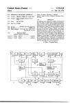
TRANSISTOR -33
UNDER TEST
35 33a
2 33a
_@_1
4
mgbi
6W v6F
I
x12?“
/8d
~46 5?
/
I2
40
22
72
(60
\ 180K 3
a
LEAD U__.>E|TRANSISTO
TEST TERM.
INDICATOR
101/
.
»
we
,8,
CONNECI
5
_.
r’
036 COLLECT
DRIVE
'
1
*[cmcu/r
57'
H‘
7
38b
39° >
BASE
DRIVE
l32b-
'
/ 1.
32'’
L-
‘92
100/
32
L
.
‘
- +
—5
,
-.
>
-
.
I
6
e;
100
_
77b
suPPLP
I03 14 I000
OOb/
‘
p
_. POWER
32d _ f
SUPPLY
"32b
l
=
,
.
/
7a
78
'
'
>
'
80/
,
"83
[85
,93
"a egLTAgA-E
"
\9a
I
“ID-1
320
77
-
400'
57
_
75
TIMING
01 -
‘’
32f’ L
'8’
6/ + i
a
1
r116 (PNP)
32¢’
32?’
I T
75
r
20‘
M"
40
'9" '98
1
. PM,
.
sw/ r614
"3"
74
'
CIR.
_,
I8 ,8
72
a
:
87a
'~
/s7
as
LEAKAGE
rssruvc
‘ 82a
CIRCUIT
é-
earn/‘6L
'
820
.
CIRCUIT
/
82
1:-
28 f
M_
m6’
2a’
326, ‘IT
U.S. Patent
Sept. 26, 1978
Sheet 4 of6
FIG.5
4,117,400
RESOAN ‘PERIOD —-—->‘
v
+5
HIGH FREQ. CLOCK PLUSES
w,
‘
O. M
+
FLIP FLOP Fl 0 OUTPUT
w
FLIP FLOP F5 0 OUTPUT
3
'FLIP FLoP F2 0’ WWW
W4
FLIP FLoP F5 0 OUTPUT
FL/P FLoP F3 0’ WWW
BASE DRIVE VOLTAGE
COLLECTOR DRIVE VOLTAGE‘ +
LOW FREQ. CLOCK PULSES
“FIG. 7
‘
I
LATCH
L
RESET
‘
TEsT mTERvALs
A
~—NPN ‘TE
PULSE-3
'
‘
’
‘
0.1!.
COLL E C TOR VOLTA GE
FOR NPN DEVICE
DIFF. GVINVERTED wAvE"OUTPUT OF OPER, AMPL.
+,
FORM FOR NPN DEV/CE AT
_
“
MAIN GATE SIGNAL FOR GATE
MAIN (GATE s/G/vAL FOR GATE
OUTPUT 0F GATE 62‘
OUTPUT 0F FLIP FLO-P
OF 6000 .NPN- TRANS.
COLLECTOR VOLTAGE FOR
PNP
DE VICE
‘
‘
‘DIFE COLLECTOR WAVEFORM
FOR PNP DEVICE AT OUTPUT
OF OPERL'AMP. 58-66
ouTPuT 0F GATE 62'
‘OUTPUT 0F‘FL/P FLoP 65'
IF GOOD PNP TRANS.
WI/
+
W‘
P TEsT
'
4,1 17,400
1.
CIRCUIT FOR TESTING TRANSISTORS OR THE
~
2
switch is preferably provided which can connect the
load and control terminal energizing and drive voltage
pulses ‘to the three terminals of a transistor or FET
under test in all the different possible connection combi
nations thereof, so that the operator does not have to
‘identify the various terminals of the transistor or FET
LIKE
BACKGROUND OF INVENTION
This invention relates to ‘circuits for testing transis
tors or FET devices for satisfactory gain both in-circuit
device to carry out the test. The low control terminal
and out-of-circuit.
drive level is selected so that with most non-bipolar
transistors a properly conducting transistor with a mod
est forward conduction current gain, for example, as
low or about 20 to 30, and shunted by a not unusually
.
-
. Until the recent development of improved testing
apparatus, transistor devices could not be tested reliably
and safely without disconnecting them from the circuits
in which they are used. When testing transistors in-cir
cuit,vwith most prior art testing apparatus there was a
low impedance, would test satisfactorily in only one of
the six different possible test switch positions. A very
signi?cant risk of damaging the circuits involved, par
marginal transistor which would pass a high level test
ticularly where the transistors-were shunted with low 15 designed to test transistors in highly shunted circuits
impedences; Thus, if DC voltages or continuous square
can, therefore, be detected and discarded if it is found
wave voltagesare applied to a heavily shunted transis-defective. Also, since most transistors will pass the low
tor, the resulting energy supplied to those circuits could
level test in only one test switch position, by color cod
be excessive and destroy associated circuit components.
ing the leads extending from the test circuit to the trans-v_
In recent years there wasdeveloped a transistor test 20 ducer under test and providing an indication to the
ing circuit using pulsed test voltage waveforms with a
low duty cycle which-‘permits transistors to be tested
safely in-circuit. Such a testing circuit is disclosedand
operator correlating the lead colors with the test switch
position, all of the transistor terminals can be identi?ed.
(In some rare cases, high-frequency transistors or tran
claimed in U.S. Pat. No. 3,870,953 to Boatman, et al. In
sistors with higher than usual gain levels may test out
this circuit, square-topped pulse waveforms are pro 25 satisfactorily in two low level drive test switch posi
vided for both the emitter-collector (load) terminals and
tions where the transistor has sufficient gain in both
the base (control) terminals of the transistor devices to
possible directions of conduction thereof, as in the case
be tested which automatically periodically establish the
voltage conditions during successive testing intervals
of symmetrical bipolar devices like FET devices.)
The high control terminal drive level is selected so
> which-test respectively NPN and PNP typetransistors.
that maximum sensitivity is achieved for testing highly
These emitter-collector and base drive voltages are
intermittently applied so that insufficient energy is ap
plied to the transistors testedin-circuit to. damage the
dition unsymmeterical bipolar transistors (i.e. transistors
shunted in-circuit transistors. However under such con
having substantially different current gain in the two
possible directions of current ?ow) having a satisfac
when low shunting impedances are present.
35 tory circuit gain will test good for two of the six possi
This transistor testing apparatus, however, did not
ble connections of the test switch under modestly low
provide for the testing of FET devices, and in other
shunting conditions, because most transistors under
respects did not give the operator maximum aid in car
these conditions will then have suf?cient forward and
transistors or the associated circuit components, even
rying out leakage and material type tests, or enable the '
reverse gain to test out satisfactorily for forward and
operator to select different control terminal drive lev 40 reverse directions of current flow therethrough. Since
els, as in the case of the present invention to be de
most good transistors will test satisfactory in only one
scribed, which has unexpected advantages to be de
test switch position during the low drive test, lead iden
scribed.
-
ti?cation can be obtained under most test ‘conditions,
‘
The present invention, .therefore, ‘represents an im
leaving the high amplitude level test for testing under
provement over the testing apparatuswhich is the sub-v 45 the most severe in-circuit shunting conditions.
ject of said U.S. Pat. No. 3,870,953.
-
FET devices can be tested in either the low or high
Accordingly, one of the objects of the invention is to
drive modes of operation of the present invention.
provide improved transistor testing apparatus operating
However, only a FET device with an unusually high
on the principle of-that disclosed in said US. Pat. No.1
gain will test good under a low drive test. Therefore, to
3,870,953, and which further permits the use of such 50 insure a valid test for all FET devices, the high drive
mode of operation of the present invention should be
apparatus
Anotherinobject
the testing
of the of
invention
FET devices.
is to provide, transis
initially used when the device being tested is known to
tor and PET testing apparatus as described which gives
be a FET device.
the operator greater ?exibility in his testing of the deIn accordance with another aspect of the present
vices involved. A' related object of the invention is to 55 invention, the base drive waveforms utilized in the com
provide transistor and FET testing apparatus which, mercial form of the Boatman circuit disclosed in said
makes it simpler for the operator to carry out material
U.S. Pat. No. 3,870,953 are modified so that FET de
type and leakage tests where the initial testing of the
vices can be reliably tested. The base drive pulse wave
devices raises the question as to whether or vnot the
forms of the Boatman et al. circuit comprises a pulse of
devices have excessive leakage. '
SUMMARY
-
THE INYENTION
In accordance with one of the features of the present
a given polarity which starts from zero at the beginning
of the test interval for each transistor type and drops to
zero after termination thereof. The zero level drive
voltages cannot render FET devices non-conductive
invention, there is preferably provided a selectionof at
and so the current transition produced in a FET device
least two widely different control terminal drive levels 65 by these waveforms do not produce current transitions
for the test circuit. "As in the ‘case also with the commer-Y»
which can be reliably detected. In accordance with the
cial form of the test apparatus disclosed in said U.S. Pat.
present invention, the control terminal drive waveforms
No. 3,870,953, a manually operable six-position test
produce current'transitions in properly operating FET
3
4,117,400
or transistor devices which can be reliably detected.
4
polarities during the application of the positive and
DESCRIPTION OF EXEMPLARY
EMBODIMENT OF THE INVENTION
Referring now more particularly to FIG. 1, the test
negative load terminal drive pulses. Such a drive signal
waveform is also operable with transistor devices which
ing apparatus shown therein includes a housing 2 in
which all of the mechanical and electrical components
are rendered non-conductive when only a zero voltage
is applied to the base terminal thereof. Thus the same
drive signal waveform is operable with both FET and
to be described are housed, and as seen from the side
These waveforms while initiating and terminating from
and to zero volts vary between negative and positive
transistor devices.
When a transistor does not show satisfactory conduc
tion under the low base drive mode of operation of the
present invention or a FET device does not show suf?
cient current gain under the high gate drive mode of
operation of the present invention, the device is re
moved from the circuit and re-tested under the appro
priate signal level conditions to determine whether or
not the device involved tested unsatisfactorily because
of high shunting impedance conditions or because of the
defective operation of the transistor or FET device.
A transistor which tests good under an out-of-circuit
condition but failed the test under the in-circuit condi
tion can be further evaluated to determine whether the
leakage thereof is excessive. In accordance with an
other aspect of the present invention, leakage tests (and
also transistor material identi?cation tests to determine
whether the device is a germanium or silicon transistor
which is necessary to perform a proper leakage test) can
be carried out without the operator concerning himself
about the selection of test voltages of proper polarity. In
this aspect of the invention when a detection operation
identi?es under a high base drive condition a transistor
of the PNP or NPN type having a satisfactory gain
level but which did not test out properly under the low
base drive test indicating a possibly leaky or heavily
shunted transistor, a test circuit voltage or proper polar
ity is automatically set up to produce a test voltage of
proper polarity for a leakage and material identi?cation
10
thereof which includes the front control panel 20. Ex
tending from the bottom of the control panel are three
differently colored connecting leads 4a, 4b, and 4c hav
ing conductive tips 60, 6b and 6c adapted respectively to
contact the unknown terminals of a transistor or FET
device while it is still connected into its normal circuit.
The leads have plug units 8a, 8b and 80 which are insert
able within jacks 10a, 10b and 100. When the test of a
transistor or FET device in-circuit indicates the need
for further testing, such device is physically removed
from its circuit and the leads extending from such de
vice are then inserted within the three apertures of
socket 12. The control panel 20 also has projejcting
therefrom the movable control arm of power on-off
switch 14 and a lamp 16 which becomes lighted when
the power on-off switch 14 is operated to its “on” posi
tion.
After power is turned on, generally the movable
control arm of a drive level control switch 15 having a
“L0” and a “HI” position is set to its “LO” position
which establishes an amplitude level for load and con
trol terminal drive current to flow in the load and con
trol terminals of a transistor which will normally be
adequate to produce a “good” transistor indication for
only one conducting direction of most satisfactorily
operating unsymmetrical bipolar transistors.
As is well known, a NPN transistor is normally oper
ated from a source of DC voltage where the positive
terminal thereof is generally coupled through a load
circuit impedence to the collector terminal and the
negative terminal thereof is connected directly or indi
rectly to the emitter terminal of the transistor. In a N
test for such a transistor after the transistor device is 40 channel FET device, a source of DC voltage is con
removed from the circuit.
nected similarly to the drain and source terminals which
The above described and other features of the inven
are respectively equivalent to the collector and emitter
tion and the advantages thereof will become apparent
terminals of a transistor. A NPN transistor or N channel
upon making reference to the speci?cation to follow
FET device is normally operated in a conductive state
and the claims.
by coupling a signal pulse or other current producing
drive voltage source so that conventional current flows
DESCRIPTION OF DRAWINGS
into the base or gate terminals, requiring generally that
FIG. 1 is a perspective view of the control panel side
the signal sources be connected so that the positive
of the housing of the testing apparatus of the most pre
terminal thereof is coupled to the base or gate electrode
ferred form of the invention;
50 and the negative terminal thereof is connected to the
FIG. 2 is a basic block diagram of the basic compo
emitter or source terminal of the transistor or FET
nents of the testing apparatus of FIG. 1;
device. A transistor is rendered non-conductive when
FIG. 3 is a circuit diagram of that part of the test
the drive voltage applied between the base and emitter
circuit including the transistor terminal switch means
terminal is zero of of a current flow opposing polarity,
and the associated function switch associated therewith;
whereas a FET device is rendered non-conductive by a
FIG. 4 is a detailed block and partial circuit diagram
drive voltage substantially different from zero and of a
of the collector and base drive circuits and the timing
current opposing polarity.
The testing apparatus of the invention now being
circuits shown in block form in FIG. 2;
FIG. 5 shows various signal waveforms present in the
described is preferably one where the operator does not
have to know beforehand the identity of the various
circuit of FIG. 4;
FIG. 6 is a detailed block diagram and partial circuit
terminals of the transistor or FET device involved. All
diagram of the detector ampli?er, gate, ?ip-?op and
that is necessary for the operator to perform a conduc
tion test under low drive or high drive conditions is
tone control and generating circuits shown in block
that, after connection of the leads 4a, 4b and 4c respec
form in FIG. 2;
FIG. 7 shows various waveforms of signals present in 65 tively to different terminals of the transistor or FET
device involved, the operating arm 18’ of a six position
the circuit of FIG. 6; and
test switch 18 is moved successively to the different
FIG. 8 is a circuit diagram of the material identi?ca
possible positions thereof until he hears a tone signal
tion circuit shown in block form in FIG. 2.
5
4,117,400
generated within the housing 2 which indicates that the
transistor or FET device involved has appreciable am
pli?cation which at least under low drive conditions
indicates a good transistor or FET device. When the
operator hears such a tone signal, he looks upon the
front panel 2a to see if a lamp 20 or 20' is lighted, which
identi?es whether the apparently good transistor or
FET device being tested is a NPN or N channel device
6
nals inserted within the sockets of the connector 12 at
the bottom of the control panel 20. If the transistor or
FET device involved did not test good under the high
drive in-circuit test, then the operator will determine
whether the transistor or FET device has a satisfactory
gain under out-of-circuit conditions by moving the test
switch 18 to its various positions to see if the lamp 20 or
20’ will become energized. If a lamp does not become
or a PNP or P channel device. As indicated, in some
energized, the operator is fairly certain that the transis
tests the transistor or FET device will test good in two
tor is defective and he can then dispose of the same.
However, if the transistor or FET device under test
out-of-circuit results in the energization of one of the
lamps 20 or 20’, then he will generally carry out further
different positions of the test switch 18, and in other
tests it will test good in only one position of the test
switch 18. Where the device tests good in only one
position, the base, collector and emitter (or gate, drain
or source) terminals of the device being tested will be
identi?ed by a color coded chart which appears in a
window 22. The chart has three different sections 20a,
20b and 20c which indicate the color of the leads 4a, 4b
and 4c which extend to the indicated terminals of the
device involved.
Visible through a window 24 on the front panel 2a of
the housing 2 are the various scales 26a, 26b, 26c, 26d,
and 26e over which a pointer 28 of a meter movement
(not shown) is moved.
If a transistor does not test good under low drive
conditions, the control arm of the drive switch 15 is
moved to. the “HI” position where the amplitude of the
tests as indicated to see whether the device tested
poorly in-circuit because of very low shunting imped
ances or because of excessive leakage after he has deter
mined whether the device is a silicon or a germanium
semiconductor device.
To this end, knob 30 of a function control switch 32
spring-urged into a center position is moved against the
return spring pressure so that a projecting nose portion
30' thereof is moved opposite a reference line 31a lead
ing to the word “IDENTIFY”. If the device involved is
a silicon device, a lamp 28 will become energized and if
25 it is a germanium device a lamp 28’ will become ener
gized. Indicia “Si” and “Ge” opposite the lamps 28 and
leakage test, then the transistor or FET device involved
28' indicate the type of semi-conductor material which
the energization of the adjacent lamps 28 and 28' are
respectively to indicate. Next, the knob 30 is rotated to
an opposite extreme position where the nose portion 30'
thereof is opposite a reference line 31b leading to the
word “LEAKAGE”. If the device is a power device,
is removed from the circuit and connected into the test
the operator then examines a scale 26d or 26e associated
control terminal drive signal is increased to make the
test circuit more sensitive. If the test of the transistor or
the FET device under high drive conditions indicates
that a further test of the device is desirable, namely a
apparatus through the socket terminals 12, as previously
with the particular type of semi-conductor material out
explained. If the operator does not know whether the 35 of which the device being tested is made, namely a
device is a germanium or a silicon device, he must de
silicon or germanium semi-conductor material. (Indicia,
termine this before carrying out the leakage test. Thus,
not shown, positioned on or opposite the scales in
it'will be noted that the leakage indicating scales 26b,
volved will identify the particular type of device in
26c, 26d and 26e have segments marked thereon of dif- '
volved for which the scale is to give leakage informa
ferent lengths, indicating the areas of the scales over 40 tion.) If the device being tested is a low signal device,
which there is a satisfactorily low leakage condition for
then the scale 26b or 26c associated with the particular
low signal and power transistors or FET devices
(which have different normal leakage currents) and/or
silicon and germanium devices which for a low signal
semi-conductor material involved is examined to deter
mine whether or not there is excessive leakage in the
device under test. If the pointer 28 moves beyond the
or power device have different normal leakage cur
usually dark colored segment of the scale involved
rents. Indicia opposite the scale 26a indicates the actual
leakage current ?ow.
indicating satisfactory leakage, the operator knows that
shunted that the transistor cannot be tested under such
drive conditions. If the transistor tests good under such
A transistor testing device operating in the manner
described is a unique test instrument since, heretofore,
low drive conditions, then the transistor is unquestion
ably a good transistor. A transistor testingbad under the
low drive conditions may test good under high drive
there has never been a single test instrument which can
the transistor or FET device has excessive leakage. The
actual amount of leakage current ?owing therein can be
If a transistor (unlike a FET device) does not test
good under low drive conditions, this may be due to a
seen by noting the indicia, not shown, opposite the ?rst
defective transistor or because the transistor is so highly 50 scale 26a.
conditions, but to be sure that the transistor is a satisfac
tory transistor for ideal circuit operating conditions the
test transistors or FET devices in-circuit as well as
out-of-circuit and where there is a selection of drive
levels which, during an in-circuit low drive test with
common levels of shunting impedances, indicates a
operator may wish to determine whether the transistor
properly operating transistor in only one of the six dif
failed a low drive condition test because of excessive
ferent possible connections of the load and control volt
leakage ‘or because merely that it was in a circuit having 60 age terminal sources to the unknown terminals of the
very low shunting impedances. If the transistor under
transistor involved, and during an in-circuit high drive
test generally indicates a properly operating transistor
or FET device for unusually low shunting impedance
transistor failed the low drive test and passed the high
without any danger of damaging the circuit. Most tran
drive test, the transistor should generally be further
tested out-of-circuit. (This applies also to FET devices 65 sistors will test good in two of the six test switch posi
which do not . test good under the high drive condi
tions in the high drive test. Moreover, the test apparatus
just described is unique in that the operator does not
tions.) The transistor or FET device to be further tested
have to concern himself in the materials determination
is then removed from the circuit involved and its termi
test failed both the low and the high drive test, or if the
7
4,117,400
of leakage tests with the conductivity type of the device
8
a waveform W8 appears which is positive only during
the NPN test interval and is negative only during the
PNP test interval. (Because of the voltage dropping
effect of associated impedances, not shown, current
?ow in the device under test will modify the voltage
appearing at output terminal 36b. The output 36b of the
collector drive circuit 36 is coupled by a conductor 41
involved since the selection of a proper polarity test
voltage is done automatically by the test circuit de
scribed.
Reference should now be to FIG. 2 which shows a
detailed block and partial circuit diagram of the most
preferred form of the present invention. FIG. 2 shows a
transistor 33 connected in-circuit with a circuit impe
dance 35 between the base terminal 33b of the transistor
and one of the load terminals 330, which will be as
sumed to be the emitter terminal of the transistor.
of the transistor terminal test switch 18. The “T”
contact of the function control switch section 320 is
(However, it is assumed that the operator of the testing
grounded.
apparatus of the invention does not know what particu
lar terminals of the transistor are the emitter, base or
collector terminals.) The test switch 18, which is shown
in block form in FIG. 2, has three switch sections 18-1,
18-2, and 18-3 as shown in FIG. 3, with input terminals
It should be apparent to those knowledgeable about
the operation of transistors and FET devices that in the
?rst half of the NPN test interval the polarities and
timing of the waveforms W8 and W7 respectively gen
erated by the collector drive and base drive circuits 36
and 38 are such that, during the NPN test interval if
they were respectively coupled to the collector and
to the “T” contact of section 32c of the function control
switch 32 where wiper 32c’ is connected to the input 180
18a, 18b, and 180 respectively extending through con
ductors 29a, 29b, and 29c to the wipers 32a’, 32b’, and
32c’ of the sections 32a, 32b, and 32c of the function 20 base terminals of the NPN transistor or the source or
control switch 32. The wipers of each of these function
drain and gate terminals of a N channel FET device,
control switch sections can selectively engage “I”, “T”,
during the ?rst half of this interval the device would be
or “L” terminals (respectively suggesting the words
non-conductive and during the second half of this inter
“Identify”, “Test”, and “Leakage”). The “I” and “T”
val the device would be switched to a highly conduc
terminals of the function control switch section 320 are 25 tive state. Similarly, the collector drive and base drive
shown grounded, and the “T” terminal of the function
waveforms W8 and W7 during the PNP test interval are
control switch section 32b is shown coupled through a
such that a PNP transistor or a P channel FET device
resistor 39 to a conductor 37 extending to the output
connected as described would be non-conductive dur
38b of a base drive circuit 38. The resistor 39 is shunted
ing the ?rst half of this interval and would be switched
by the section 15a of the drive control switch 15 when 30 to a highly conductive state during the second half of
the switch is in its “HI” position.
this interval.
The base drive circuit 38 has an input 38a controlled
The test switch 18, as shown in FIG. 3, has three
by a timing circuit 40 so that there appears at the output
switch sections 18-1, 18-2, and 18-3 with associated
38b a base terminal drive voltage waveform W7 which
wipers 18-1’, 18-2’, and 183' which make contact with
is negative during the ?rst half of an NPN (or N chan
nel) device test interval and is positive during the sec
ond half of this test interval, and which is positive dur
ing the ?rst half of the immediately successive PNP (or
P channel) device test interval and is negative during
six associated stationery contacts interconnected in
such a way that the three inputs 18a, 18b, and 180 of the
test switch 18 are connected in six different ways to
output terminals 18d, 18a, and 18f thereof, whereby the
collector and base drive waveforms are applied in the
the second half of this test interval. These two succes 40 six different possible ways to the output terminals 18d,
sive test intervals are repeated each cycle of operation
of the circuit shown, which cycle repeats itself at a
given rate where the period occupied by the two test
intervals described is a small fraction of the total period,
18e, and 18f
The output terminals 18d, 18c, and 18f of the test
will have relatively high and relatively low values.
The timing circuit is synchronized by a slow clock
pulse generator 43 which generates pulses at a relatively
slow frequency, for example, 10 hertz. Accordingly, the
output 43b of the slow clock pulse generator 43 is
switch 18 (which input terminal is connected as previ
ously described to the output of the base drive circuit
38) is connected to the base or gate (control) terminal of
switch 18 connect respectively to the connecting leads
4a, 4b, and 4c and to the associated terminals of socket
referred to as a rescan period in FIGS. 5 and 7, between 45 12. The conductive tips 6a, 6b, and 6c associated with
the successive generation of waveform W7. This pro
the leads 4a, 4b, and 4c are respectively connected to
vides a low duty cycle and relatively low energy ap
any of the exposed terminals of the transistor or FET
plied to the transistor or FET device under test to avoid
device under test without the operator knowing before
damage to the circuit in which the transistor or FET
hand which particular terminals are the load or control
device is located. It is apparent that when the drive 50 terminals of the device under test. The waveforms W7
control switch 15 is respectively in its “L0” and “HI”
and W8 are such that a transistor or FET device will
positions, the current resulting from the waveform W7
not test good unless the input terminal 18b of the test
shown connected by a conductor 45 to a synchronizing
input 400' of the timing circuit 40. The timing circuit 40
55
the transistor or FET device under test. Also, in case of
an unsymmetrical bipolar transistor, the input terminal
18c associated with the collector drive circuit 36 must
be connected by the test switch to the collector terminal
of the transistor under test for the transistor to test
is also controlled by a fast clock pulse generator 42
which has an input 42a synchronized from the slow
satisfactory under low drive conditions (except in the
clock pulse generator 43, and an output 42b where
case of special transistors which have suf?cient reverse
pulses appear, for example, at a frequency of 1,000
gain to test satisfactory under such low drive condi
hertz. The pulses are fed to the synchronizing input 40a
tions).
of the timing circuit 40.
65
The point in the circuit just described at which the
The timing circuit 40 also controls the voltage wave
voltage conditions are sensed to determine whether or
form generated by a collector drive circuit 36 having an
not the device being tested has a satisfactory gain is the
output terminal 36b at which under no load conditions
output of the collector drive circuit 36 which should be
9,
4,117,400‘
10
coupledv through the function control switch section 320
proper polarity (positive) pulse fed to the input 62a
directly to one of the load terminals, generally‘ the col?
thereof only during the second half of the NPN test
interval, and prepare the gate 62' for opening by a posi
tive pulse fed to the input 62a’ thereof only during the
lector of an unsymmetrical bipolar 1 transistor‘ device
under test, to obtain a good gain indication. When the
output terminal 36b of the collector drive circuit is
second half of the PNP test interval. While the gate 62
connected to the collector of a satisfactorily operating
is prepared to be opened during the NPN test interval,
NPN transistor or either load terminal of a satisfactorily
operating N channel FET device, as previously indi~
cated because of the voltage dropping effect of various
impedances connected to the output terminal 36b of the
the polarity of a pulse developed at the output of the
detector ampli?er and inverter 58 due to a properly
operating PNP transistor or equivalent FET device will
not open the gate 62. Similarly, during the time that the
collector drive - circuit, the voltage which appears
thereat will be different from'the collector drive wave
interval, the polarity of the pulse fed to the input 62a’
gate 62"is prepared for opening during the PNP test
form W8, namelythat'shown by the waveform W10 in
thereof will be of the incorrect polarity to open the gate
62' when a properly operating NPN transistor or equiv
alent FET device is being tested.
The output terminals 62b and 62b’ of the gates 62 and
62’ are respectively connected to the input terminals
650 and 65a’ of ?ip-?op circuits 65 and 65’, which re
FIG. 7. The waveform appearing at the output of the
collector drive circuit 36 when a properly operating
PNP transistor or P channel FET device is being tested
is shown by the waveform W16 in FIG. 7. The voltage
changes shown by these waveforms W10 and W16 will
not occur when an improperly operating transistor or
FET device is being tested and any pulses generated by
20
the differentiation of such'voltages- will not be of suf?
spectively are set by a positive pulse passing through
the open gates 62 and 62'. The setting of either ?ip-?op
65 or 65’ will energize the associated indicating lamps
cient amplitudeto operate the detecting circuits in the
20 or 20’ which are shown connected to ground. Also,
manner now to be described when a properly operating
the setting of either flip-flop 65 or 65' will operate a tone
transistor or FET device is being tested.
generator circuit 64 in any suitable way. As illustrated,
A conductor 52‘ extends from the collector drive 25 the output terminals 65b and 65b’ of the ?ip-?op circuits
output conductor 41 to the input portion of a detecting
65 and 65' are respectively shown connected to a NOR
circuit which, as illustrated, includes a resistor 53
gate 72 which will pass the voltage at the terminal 65b
shunted by the section 15b of the drive control ‘switch
or 65b’ of a set ?ip-?op 65 or 65', to energize a tone
when this switch is in its‘ “HI” position, so that the
generator circuit 74 to which a loudspeaker 76 is con
detector circuit then operates-withv maximum sensitivity 30 verted. In the most preferred form of the invention, the
under these conditions, to increase the signal» to noise
tone generator circuit 74 is in condition for operation
ratio therein. Resistor 53‘ is'connected to a differentiat
only during the intervals between the NPN and PNP
ing network 54'which differentiates the waveform aptest intervals. Accordingly, a control conductor 75 is
pearing on the collector drive output conductor 41.
shown extending between an output of the timing cir
When the waveforms W10 and W16 are differentiated 35 cuit 40 and the tone generator circuit 74, to couple a
by the network 54, comprising a capacitor-54 in series
with a grounded resistor 56a, the voltage appearing
across resistor 560 will be that shown respectively by
the W11’ and W1_7' waveforms shown only in FIG. 2. It
should be noted that the pulses P1 and P1" occurring
during the ?rst polarity transition of the base drive
waveform W7 are of opposite polarity respectively for
properly operating NPN and PNP transistors (or their
equivalent conductivity type FET devices), and that,
similarly, the pulses P2 and P2’ occurring respectively
for properly operating NPN and PNP transistors (or
their equivalent conductivity type FET devices), dur
ing the second polarity transition of the waveform W7
signal which prevents operation of the tone generator
circuit 74 during the test intervals. Also, in the particu
lar circuit shown in FIG. 2, a section 32f of the function
control switch 32 is provided which prevents operation
of the loudspeaker 76 when the function control switch
32 is in its “I” or “L” positions during the materials
identi?cation and leakage test operation of the testing
circuit described. Accordingly, only the “I” and “L”
45
contacts of this switch section are shown grounded.
The ?ip-?op circuits 65 and 65’ are reset once during
each cycle of operation of the described testing circuit
(except where the function control switch is held in the
“LEAKAGE” or “IDENTIFY” positions). To this
end, connections are shown from the slow clock gener
scribed, amplify and inverts the waveforms W11’ and 50 ator 43 to the rest inputs 65c and 65c’ of the ?ip-?op
circuits 65 and 65’.
W17’ and sense them only during the polarity transition
are also of opposite polarity. The circuits to be de
periods of the waveform W7, to identify'proper'ly oper
ating NPN or PNP devices (or FET devices of equiva
leakage test is not carried out except where a transistor
lent conductivity type).
or FET device in an out-of-circuit test tests satisfactory,
It will be recalled that a material identi?cation or
While this detecting circuit can accomplish this result 55 but failed either or both the low or high drive tests,
in a number of ways, as illustrated in the prefered form
indicating the possibility that the transistor or FET
of the invention of FIG. 2, the output of differentiating
device involved has excessive leakage therein or that
network 54 is shown connected to a detector ampli?er
the transistor was located in a heavily shunted circuit.
inverter 58 (which may be an operational ampli?er
Thus, when such a transistor or FET device tests satis
which inverts and ampli?es waveforms W11’ and W17’ 60 factory in an out-of-circuit test, (or at any other time
to produce the waveforms W11 and W17 in FIG. 7).
when the transistor tests satisfactory), a test voltage
This ampli?ed and inverted output is fed to the input
supply circuit 77 is automatically operated to provide at
its output 77b a DC voltage of proper polarity to carry
620 of a gate 62 and also to the input 660 of an inverter
out a materials or leakage test for the NPN or N channel
66. The output 66b of the ‘inverter 66 is fed to the input
620' of a gate 62’. The timing circuit~40 produces output 65 device or- for the PNP or P channel device involved.
signals fed to one or more input terminals of the gates 62
Accordingly, the test voltage supply device 77 has an
input 770 connected by conductor 81 to the output 65b
and 62', such as the‘ “inputsv 60c and 60c’ ‘illustrated,
which signals prepare ‘the gate 62 ‘for opening by a
of one of the ?ip-flop circuits 65. If either one of the
11
4,1 17,400
lamps 20 or 20’ is energized showing a properly operat
ing transistor or FET device, the output of the ?ip-?op
12
leakage test, one load terminal and the control terminal
of the device under test are connected together and the
leakage is measured between these terminals and the
other load terminal thereof. To this end, the “L”
contact of the function control switch sections 320 and
32b are respectively connected together by a conductor
91 and the conductor 91 is connected by conductor 93
to an input 870 of the leakage testing circuit 87. Thus,
when the function control switch is moved to the “L”
circuit 65, which will then be either a positive or a zero
voltage, will identify whether the device involved is an
NPN or N channel device (namely, when the output
thereof is positive), or whether it is a PNP or P channel
device (namely, when the output thereof is zero). The
DC test voltage supply circuit 77 will provide a DC
output 77b of one polarity when the output of the ?ip
?op circuit is positive and it will provide an output of
position thereof, the wipers 32a’ and 32b’ of the function
the opposite polarity when the output of the ?ip-?op
control switch sections 320 and 32b will connect the
circuit 65 is zero.
conductor 93 to the control and one of the load termi
During the performance of a materials or leakage test,
it is imperative that the normal transistor test cycle be
nals of the device under test. The other load terminal of
the device under test is coupled by the test switch 18 to
terminated and the set or reset condition of the ?ip-?op 5 the wiper 320' of the function control switch section '
32c, in turn, coupled through the “L” contact of the
circuit 65 or 65’ be maintained, so that the test voltage
switch section, a conductor 92, and resistor 98 of a
supply circuit 77 will have a steady output of proper
voltage divider network including a grounded resistor
polarity to carry out the materials and leakage tests.
99 to the aforementioned conductor 78 extending to the
Accordingly, the slow clock pulse generator 43, which
normally applically resets the ?ip-?op circuits 65 and
65’, is de-energized during these materials and leakage
tests. To this end, FIG. 2 shows a function control
switch section 32d having a grounded wiper 32b’ and a
connection extending only from the “T” contact to the
slow clock pulse generator 43. Accordingly, the slow
clock pulse generator 43 has no continuity to ground
20
output terminal 77b of the test voltage supply circuit 77.
It is thus apparent that the output voltage of the test
voltage supply circuit 77 is coupled in series with the
two unconnected terminals of the device under test to
the input of a leakage testing circuit 87 of conventional
25 design which feeds a current through the meter move
ment 89 in proportion to the degree of leakage current
involved. The test voltage supply output must have a
and therefore is decoupled from its supply source when
de?nite polarity relationship with respect to the uncon
the wiper 32b’ is connected to the “L” and “I” contacts.
nected load and the base terminals of the device under
The materials testing circuit identi?ed by reference
number 82 in FIG. 2 has an enabling input terminal 820 30 test if the device is a non-bipolar transistor.
FIG. 2 shows a block 100 representing a DC power
connected by a conductor 83 to the output of NOR gate
supply having an output 100a at which a +5 volt with
72 so that the material testing circuit is prepared for
respect to ground voltage appears and an output 100b at
operation only when either the ?ip-?op circuits 65 or
which a —5 volt with respect to ground voltage ap
65' is set, indicating an apparently properly operating
pears. Also shown is the aforementioned power on-off
transistor or FET device. A conductor 78 extending
switch 14 and the power indicating lamp 16 connected
from the output 77b of the test voltage supply circuit 77
in a conventional way to AC. input conductors of a
is shown coupled through a resistor 80 and a conductor
plug connector 103 thereshown.
85 to the input terminal 82a’ of the material testing
FIG. 2 also shows in block form a lead connection
circuit 82. The input terminal 820‘ of the material testing
circuit is also shown connected by a conductor 88 to the 40 indicator 101 which is mechanically coupled to the test
switch 18. The lead connection indicator may comprise
“I” contact of the function control switch section 32b
a movable member (not shown) which responds to the
which contact, when a properly operating transistor has
movement of the test switch 18 to its six different posi
been detected, is connected through the wiper 32b’ and
tions. In each of these different positions of the test
the test switch 18 to the control terminal of the transis
tor or FET device being tested. The “I” contact of the 45 switch 18, a different color coded chart having a differ
ent section 21a, 21b, and 210 becomes visible in the
function control switch section 32a is grounded so that
window 22 of the control panel 2a. The color of these
the control terminal and one of the load terminals of the
device under test during a materials test are connected
between the input terminal 820’ of the material testing
circuit 82 and ground. The testing circuit 82 to be de
scribed, is one wherein the circuit is responsive to the
different voltage drops which occur between the termi
nals of the device under test when the devices are re
spectively silicon and germanium semiconductor de
vices. The circuit 82 energizes either the lamp 28 or 28',
depending upon the value of this voltage drop. The
lamps 28 and 28' are rendered inoperable except during
the materials and leakage test by the connections
three different sections visible in the window 22 corre
sponds to the colors of the leads 4a, 4b and 40 which
would be extending respectively to the base collector
and emitter of a non-bipolar transistor under test where
the test circuit indicates that the transistor is a properly
operating one for the particular test switch position
involved.
Both the particular block diagram circuits shown in
FIG. 2 and the particular details of any of the circuits
shown in block form therein to be described can vary
widely without deviating from the broad aspects of the
invention. However, FIG. 2 shows the most preferred
thereof shown in FIG. 2 to the wiper 320' of switch
section 32e of the function control switch 32. Thus, the 60 logic circuit of the invention and the circuits now to be
described show the most preferred forms of the cir-*
“I” and “L” contacts of this switch section have no
cuitry for some of the circuits shown in block form in
connections thereto and the “T” contact thereof is
FIG. 2. Accordingly, reference should now be made to
grounded, so that these lamps are rendered inoperable
FIG. 4 which, among other things, shows the preferred
except during a materials and leakage tests.
circuit for the timing circuit 40 and the collector and
The output of the test voltage supply circuit 77 is also
base drive circuit 36 and 38. The timing circuit 40 com
connected to a leakage testing circuit 87 which may be
of conventional design. The leakage testing circuit 87
controls the operation of a meter movement 89. In a
prises a series of toggle ?ip-?op circuits F1, F2, and F3
which have enabled input terminals E and reset input
13
4,1 17,400
terminals R to which positive voltage must be fed to
enable the ?ip-?op circuit to be set and reset (i.e. tog
gled) by successive pulses fed to toggle input terminals
T thereof from the input of the fast clock pulse genera
tor 42. The output thereof, shown by waveform W9 in
FIG. 5, is a normally +5 volt output which drops mo
14
positive enabling voltage on its enable input terminal
which lasts for the duration of the NPN and PNP test
intervals. There is thus produced at the Q output of the
toggle ?ip-?op circuit F1 a voltage waveform W2 (see
FIG. 4 or FIG. 5) which is coupled by a conductor 121
to the toggle input terminal T of the toggle ?ip-?op
mentarily to zero volts at a 1000 Hertz rate. The reset
circuit F3 and by a conductor 123 to the detector gates
input terminal R can also be used to reset the ?ip-?op
62 and 62'. The positive going portions of the wave
forms W2 occur during the second halves respectively,
of the NPN and PNP test intervals, during which the
pulses resulting from the differentiation of the collector
circuits to a reference reset condition when a zero or
negative going voltage is applied thereto. Each of these
toggle ?ip-?op circuits have Q and Q’ output terminals.
The voltage at each Q output terminal will be positive
when the ?ip-?op circuit involved is in a set condition
and will be at zero voltage when the circuit is in a reset
condition. The voltage at each Q’ output terminal is
opposite to that of the L output terminal (i.e. it is zero
when the other is positive and vice versa).
.The timing circuit further has a ?ip-?op circuit F5
having set and reset input terminals S and R respec
terminal voltage waveforms like W10 and W16 are to
be detected, to identify whether or not there is a satis
factory operating transistor or FET device.
It will be recalled that only a zero or negative going
voltage will effect a setting operation in any of the
?ip-?op circuits just described and, therefore, a connec
tion of the Q output of the toggle ?ip-?op circuit F1 to
the toggle input terminal T of the toggle ?ip-?op circuit
tively and output terminals Q and Q’ and which will
F3 will not result in a toggling of ?ip-?op circuit F3
have the same voltages as the Q and Q’ terminals of the
toggle ?ip-?op circuits F 1, F2 and F3 just described in
except during the zero going portions of the waveform
W2. Accordingly, the waveform appearing at the Q
output terminal of the ?ip-?op circuit F3 will have the
the set and reset conditions states thereof. The feeding
of a zero or negative going pulse to the set input termi
outline of waveform W5 of FIGS. 4 and 5, which is
nal» S will result in the setting of the ?ip-?op circuit F5 25 positive only during the PNP test interval. Waveform
and the feeding of a similar voltage to the reset terminal
W5’ is the waveform appearing at the Q’ output termi
R of the ?ip-?op circuit F5 will result in the resetting of
nal of the ?ip-?op circuit F3 and it is zero during this
the ?ip-?op circuit F5. The timing circuit further in
test interval.
cludes inverting “NAND” gates 102 and 102' having
A conductor 125 extends from the Q’ output of the
pairs of input terminals l02a-102b and 102a’—102b'. The
toggle ?ip-?op circuit F1 at which terminal the wave
output voltage of each gate 102 or 102’ will be normally
form W2’ of FIG. 4 appears to the toggle input terminal
+5 volts and will drop to zero volts when both input
T of ?ip-flop circuit F2. Since the toggle ?ip-?op cir
terminals thereof have +5 volts voltage fed thereto.
cuit F2 is toggled only during a zero going pulse fed to
The slow clock pulse generator 43 generates negative
the T input terminal thereof, the waveform W4 appears
going pulses at an exemplary rate of 10 per second. As 35 at the Q’ output terminal thereof, which waveform is
shown by waveform W1 in FIG. 5, the generator 43
positive except during the second half of the NPN test
normally has a + 5 volt input which momentarily drops
interval and the ?rst half of the PNP test interval. Thus
to zero at ‘the 10 Hertz rate. These pulses are fed by a
the waveform W4 is a zero going pulse centered over
conductor 104 togthe set input terminal S of the ?ip-?op
the middle portion of the NPN and PNP test intervals.
circuit F5 which causes the voltage on the Q’ output 40 The waveform W3 which is positive during the dura
terminal thereof (see waveform W3’ in FIG. 6) to drop
tion of these test intervals, and the waveform W4 which
from a positive to a zero voltage level which-remains
is zero during a period centered within the test intervals
for the duration of the NPN and the PNP test intervals
are utilized to generate the base drive voltage wave
form W7 shown in FIG. 5.
previously described. The voltage on the Q output ter
minal thereof (see waveform W3 in FIGS. 4 and 5) 45 The waveform W3 generated by toggle ?ip-?op cir
cuit F5 is fed by conductors 118 and 128 to the input
which is positive during ‘the NPN and PNP test inter
102b of a “NAND” gate 102 and the waveform W4
vals is fed by conductors 113, 115, 118, 120 and 119 to
the reset and enable terminals of toggle ?ip-?op in
generated by toggle ?ip-?op circuit F2 are fed by con
cludes F1, F2, and F3 to prepare them for operation. A
ductors 130 and 132 tov the input 1200 of a “NAND”
conductor 105 extending from the Q’ output terminal of 50 gate 102. The outputs 102c of “NAND” gate 102 is
?ip-?op circuit F5 extends to the previously mentioned
coupled through a resistor 134 to the base 135b of a
NOR gate 72 controlling the tone generator circuit 74.
PNP transistor 38 whose emitter 135a is connected to a
‘ 'The negative or zero going pulse output from the
+ 5 volt bus 140. The collector 1350 of the transistor 135
slow clock pulse generator 43 is fed by conductors 106
is coupled through a resistor 137 to the base 13% of
and 108 to the reset input terminal R of the toggle ?ip 55 PNP transistor 139. The emitter 139a of the transistor
flop circuit F1 to prevent this circuit from being set at
139 is connected to —5 volt bus 142. The collector 139c
that instant. The same pulse is fed through a recti?er
of the transistor 139 is coupled to the collector 144a of
110 to a terminal 42b of the fast clock pulse generator to
a PNP transistor 144 whose emitter 144a is connected to
synchronize the same. In the particular circuit illus
the +5 volt bus 140 and whose base 144b is connected
trated, the terminal 42b is also the output terminal for 60 by a conductor 145 and resistor 151 to the emitter 144a.
the pulses generated by the pulse generator 42. These
pulses are fed to toggle input terminal T of the toggle
A conductor 145 and a resistor 147 connects the base
144b to the conductor 130 upon which the waveform
?ip-?op circuit F1. Accordingly, a conductor 111 ex
W4 appears.
tends from the terminal 42b to toggle input terminal T
It should be apparent that when the waveform W4,
of the ?ip-?op circuit F1. Thus, the second pulse gener 65 which varies between +5 volts and zero, is at +5 volts,
ated by the fast clock pulse generator 42 will toggle the
the voltage difference between the emitter and the base
flip-?op circuit F1 as does each succeeding pulse
of the transistor 144 is zero, since the emitter is con
nected to the +5 volt bus 140. Zero volts applied to the
thereof, so long as the ?ip-?op circuit F1 receives a
15
4,117,400
base of a PNP transistor results in termination of collec
tor current. Transistor 144 becomes conductive when
the waveform W4 drops to zero, which occurs during
16
coupled through resistor 163 to the base 13512’ of the
transistor 135’ driving transistor 139’. The transistor
135' is therefore conductive during this test interval
during which the waveform W5’ remains zero.
the second half of the NPN testing interval and the ?rst
half of PNP testing interval, since then the base 144b is
negative with respect to the emitter 1440.
Refer now to FIG. 6 which shows, among other
things, exemplary circuits for the detector ampli?er and
inverter circuit 58, inverter 66, gates 62 and 62’, ?ip-?op
When the waveforms W4 and W3 are applied to the
inputs 102a and 10211 of the gate 102, prior to the begin
circuits 65 and 65', NOR circuit 72 and the tone genera
ning of the NPN test interval the voltage at the input
tor circuit 74 shown in block form in FIG. 2. FIG. 6
1020 will be +5 volts and the voltage at the input termi 10 shows the detector ampli?er and inverter 58 circuit as
nal l02b will be zero volts, so that its output terminal
an operational ampli?er with the negative inverting
102:: will be at +5 volts and the adjacent transistor 135
will be non-conductive. However, at the start of the
NPN test interval and until the point where the wave
form W4 reduces to zero, both inputs to the gate 102
will be positive, so that the gate output terminal 102a
input terminal 580 thereof connected to the output ter
minal 58b of the ampli?er through a resistor 54b, which
also forms a part of the differentiating network includ
' ing the capacitor 54a. The positive input terminal 580 of
will drop to zero, thereby causing the transistor 135 to
become conductive. This, in turn, drives the transistor
139 conductive to couple the —5 volt bus 142 to the
collector circuit point 153’ coupled by the resistor 155 20
the operational ampli?er is shown grounded. As previ
ously described, the output of the operational ampli?er
58b is coupled to the input 620 of the gate 62’ which is
a “NAND” gate. Similarly, the output 66b of the in
verter 66, whose input 66a is connected to the output
and the previously mentioned resistor 39 to a base drive
terminal 58b of the operational ampli?er 58, is con
terminal 157 connected to the “T” contact of the func
nected to the input 62a’ of the gate 62' which is also a
tion control switch section 3212.
“NAND” gate. While in FIG. 2, the gates 62 and 62' are
As previously indicated, when the waveform W4
shown with only a single gating input (since this is a
drops to zero, the “NAND” gate 102 will close, and this 25 generalized or simpli?ed circuit), the gate 62 of FIG. 6
portion of the waveform W4 coupled through the resis
has two gate signal input terminals 62c-1 and 62c-2 and
tor 147 to the base of transistor 144, will render this
the gate 62’ has two gate signal input terminals 62c-1’
transistor conductive, thereby coupling the + 5 volt bus
and 62c-2’. The gate signal input terminals 620-2 and
140 to the point 153’ coupled to the base drive terminal
62c-2’ of the gate 62 and 62’ are connected to the con
157. The transistor 144 remains conductive until the
ductor 123 previously described in connection with
waveform W4 once again rises to a + 5 volt level, when
FIG. 4 on which conductor the waveform W2 appears
the aforementioned transistors 135 and 139 will become
which goes positive only during the second half of the
conductive for the second half of the PNP test interval,
NPN test interval and the second half of the PNP test
after which the dropping of the waveform W3 to zero
interval, so that the gates 62 and 62’ are prepared for
will result in both transistors 144 and 139 being non 35 opening during these periods. However, the gate 62 is
conductive, so that the voltage at the base drive termi
prepared for opening only during NPN test interval by
nal 157 will be zero.
the connection of its gating signal input terminal 620-1
The collector drive ,waveform W8 (FIG. 5) is gener
ated by the feeding of the waveforms W3 and W5 of the
Q and Q’ outputs of the ?ip-?op circuits F5 and F3 to
the inputs 102b’ and 102a’ of the “NAND” gate 102'
through conductors 113, 115, 118, 128, and 133 and 136.
The output terminal 1020' of this gate‘; is coupled
to a conductor 136 upon which appears the waveform
conductor 129 upon which waveform W5 appears,
through a resistor 134' to the base 144b’ of a PNP tran
which is only positive during the PNP test interval.
W5’ which is always positive except during the PNP
test interval when it is zero. The gate 62' is prepared for
opening only during the PNP test interval by the con
nection of its gate signal input terminal 620-1’ to the
sistor 144’ forming part of the collector drive circuit 36, 45
which is a circuit similar to the base drive circuit 38 just
As previously indicated, only a properly operating
NPN transistor results in the presence of a positive
described. The corresponding components of the cir
pulse at the output of the gate 62 during the polarity
cuits 36 and 38 will be similarly numbered, except that
transition of the base drive waveform W7 from its nega
a prime (') has been added to the elements of the circuit
tive to its positive polarity during the NPN test interval,
36. However, the connections of the gate 102' and other 50 and a properly operating PNP transistor results in a
associated portions of the circuit to the collector drive
positive pulse at the output of gate 62’ during the polar
circuit 36 are different from those connections made
ity transition of the base drive waveform W7 from its
from the gate 102 and associated portions of the base
positive to its negative polarity during PNP test inter
drive circuit 38 to the transistors of the base drive cir
, val. The pulse at the output of gates 62 and 62' are fed
cuit 38. Accordingly, the output terminal 1020’ of the
gate 102', which is normally at +5 volts, will normally
render the transistor 144’ non-conductive until the gate
102' has opened by the transition of the waveform W3
55 to the set input terminals 650 and 650’ respectively of the
from zero to +5 volts at the beginning of an NPN test
?ip-?op circuits 65 and 65'.
The output terminals 65b and 65b’ of the ?ip-?op
circuits 65 and 65' are Q’ output terminals which have a
+5 volt output when the ?ip-?op circuit involved are
interval when the waveform W5’ is still positive. The 60 reset and a zero voltage when the ?ip-?op circuits are
set. At the beginning of each NPN test interval, the
reset input terminals 65a and 65a’ of these gates are
resistor 39'.
respectively fed with a zero going pulse from the slow
At the initiation of the PNP test interval, when the
clock pulse generator 43 to minimize any continued
waveform W5’ drops to zero, the gate 102’ will re-close, 65 false operation clue to occasional transients. The clock
to render the transistor 144’ non-conductive, and the
pulses are fed on conductor 69.
waveform W5’, then dropping to zero, is effective to
The Q’ output terminals 65b and 65b’ of the ?ip-?op
render the transistor 135 conductive, as this voltage is
circuits 65 and 65’ are respectively coupled to the inputs
conduction of transistor 144' will thus cause + 5 volts to
appear at the collector drive terminal 157' adjacent to
4,1 17,400
17
72a and 72a’ of the “NOR.” gate 72. “NOR” gate 72, as .
illustrated, is a circuit wherein the voltage at the output
terminal 72b thereof is normally zero and will the posi
tive if any one or more inputs thereof are at zero volts...
If no transistor is being tested or the transistor being .
tested does not pass the gain test, the Q’ outputs; of the .
?ip-?op circuits 65 and 65’ will be positive.
When the NOR gate output is positive, the positive
voltage is fed by a conductor 139 to the reset input
terminal R of a toggle ?ip-?op circuit F4 like the other
toggle ?ip-?op circuits F1, F2, and F3 previously de
scribed. To permit the ?ip-?op circuit‘F4 to toggle,
18
resistor 164 connected to the emitter 162a of the transis
tor162, in turn, connected to the +5 volt bus 140.
, Accordingly, when the Q’ output of the ?ip-?op
circuit 65 is at zero volts, indicating a satisfactorily
operating NPN transistor under test, this zero voltage
coupled through resistor 160 to the NPN transistor 162
will render the transistor 162 conductive, to couple the
voltage of the +5 volt bus 140 to the collector side of
the transistor 162, in turn, connected through the resis
tor 80 to the conductor 88 (FIG. 2) leading to the “I”
contact of the sections 32b of the function control
switch 32. The collector side of the transistor 162 is also
connected through the resistor 98 to the “L” contact of
the section 32b of the function control switch, which
both the enabling input terminal E and the reset termi
nal R must have a positive voltage thereon. To this end,
the waveform W3’ at the output of the ?ip-flop circuit 15 forms part of the leakage test circuit as previously ex
plained.
F5 (FIG. 4) is coupled by a conductor 137>to the en
When the Q’ output terminal of the ?ip-?op circuit 65
abling terminal E of the ?ip-?op circuit F4. The wave
is positive, indicating an apparently satisfactorily oper
form W3’ is normally positive and goes zero only dur
ating PNP transistor, this positive voltage effects con
ing the very short period occupied by the NPN and
PNP test intervals (0.004 second) during each rescan 20 duction of the base grounded transistor 156 which, in
turn, renders the transistor 158 conductive to couple the
period (0.1 second). The length of time that the enabling
—5 volt bus 142 to the collector side of the transistor
terminal of the ?ip-?op circuit receives this zero volt
age from the line 137 is of very short duration and re- ' 158 and through ‘the resistor 80 and 98 to the circuits
which perform the material and leakage tests. (As previ
peats at a low rate of 10 cycles per second but itmodi
ously indicated, the state of ?ip-?op circuit 65 is locked
?es the sound generated by the loudspeaker 76 so that it
in when the function control switch 32 is moved from
is a more easily noticeable raspy sound. The toggling
its
center position to either the “I” or “L” positions
input terminal T of the ?ip-?op circuit F4 receives its
thereof.)
input from the output of the fast clock pulse generator
Reference should now be made to FIG. 8 which
42 on conductor 141. The zero going fast clock genera
shows a preferred but exemplary circuit for the material
testing circuit 82. It will be recalled that the input termi
nal 82a’ of this circuit is coupled through conductors 88
while the enabling and reset terminals E and R thereof
and 85, and resistor 80 to conductor 78 leading to the
receive a positive voltage in the periods between the
NPN and PNP test intervals. The ?ip-?op circuit F4 35 output terminal 77b of this test voltage supply 77. Also,
the function control switch section 32b when its wiper
has a Q output which during the toggling of the circuit
32b’ engages the “I” contact connects one of the load
comprises positive pulses fed to the base 43b of a NPN
terminals and the control terminal of the device under
transistor 143 by a conductor 142. The collector 143s of
test between the input terminal 820’ of the material
the transistor 143 is connected to the +5 volt bus 140
testing circuit 82 and ground. Moreover, the polarity of
and the emitter 143a of the transistor 143 is connected 40 ‘the DC voltage fed to the input terminal 820’ depends
through resistor 145 to the terminals of loudspeakers 76,
upon whether the device under test is of one conductiv
in turn, connected to ground.
ity type or another since the voltage drop which is
The lamps 20 and 20', which are shown as light-emit
measured in ‘he materials test to determine whether the
tor pulses are effective in repeatedly switching the tog
gle ?ip-?op circuit F4 between its set and reset states,
ting diodes, are respectively connected between the Q’
material is a silicon or germanium material must be that
output terminals of the gates 65 and 65' and a common 45 produced by current ?ow in the low impedance direc
terminal 150 connected through a resistor 152 to the + 5
tion of the control terminal to load terminal junction.
volt bus 140. It is apparent, therefore, that when either
The material testing circuit 82 includes reverse con
of the Q’ outputs of the ?ip-?op circuit 65 or 65‘ is zero
because of the set condition thereof, the associated lamp
20 or 20' will become energized.
7
nected recti?ers 160 and 162 respectively connected
between the input terminal 82a’ and the respective in
50
verting and non-inverting input terminals 164a and
As previouslyindicated, when either the lamp 20 or
20' is energized indicating to the operator that there is a
properly operating transistor or FET device and the
operator desires to carry out a leakage test, the condi
tion of the ?ip-?op circuit 65 will indicate whether the 55
1640' of an operational ampli?er 164. A feedback resis
tor 170 is connected between the output terminal 164b
and the inverting input terminal 164a. For an NPN or N
transistor orv FET device under test is a NPN (or N
device this voltage drop is negative. If the negative
voltage drop is greater than —0.4 volts, which is pres
ent for a silicon device, this voltage exceeds the thresh
channel) or a PNP (or P channel) device. Accordingly,
a conductor 153 extends between the Q’ output 65b of
channel device the voltage drop between the control
and load terminal is positive and for a PNP or P channel
the ?ip-?op circuit 65 and a resistor 154, in turn, con
old of the recti?er 160, which is a silicon reciti?er with
nected to the emitter 156a of aPNP transistor 156 of the 60 a reverse threshold of 0.4 volts. This negative voltage is
test supply circuit 77. The base 156b of transistor 156 is
grounded and the collector 156a thereof is connected to
the base 158b of a NPN transistor ‘158. The emitter 158a
applied to the input terminal 1640 of the operational
ampli?er 164 to produce a +5 voltage at the output
terminal 164b thereof. If the base to emitter voltage
of transistor 158 is connected to the ~.- 5 volt bus 142 and
involved exceeds +0.4 volts, which is indicative of a
the collector158c thereof is connected to the collector 65 silicon device of opposite conductivity type to the de
162a of a PNP transistor 162. The base 162b of the tran
vice which produced a voltage in excess of 0.4 volts,
sistor 162 is connected through the resistor 160 to the
this voltage is coupled through the recti?er 162, which
?ip-?op circuit output conductor 153 and‘ through a
is also a silicon recti?er, to the input terminal 1640' of
19
4,1 17,400
the operational ampli?er which then produces + 5 volts
at the output terminal 164b thereof. When neither of the
input terminals 1640 or 1640’ receives a voltage through
the recti?er 160 or 162, the output of the operational
ampli?er will be at zero volts. This occurs when the
device under test is a germanium device which pro
duces a control to load terminal voltage drop of less
than 0.4 volts.
When the voltage at the output terminal 164b is +5
volts, this voltage is applied to one of the terminals of 10
the light emitting diode or lamp 28, in turn, connected
through resistor 182 and the collector 184c and emitter
1840 of an NPN transistor 184 to the “I” and “L” termi
nals of the section 32e of the function control switch 32.
The switch section 32c has a wiper 32e’ which is
20
produce different current transitions unless collector
and base drive circuits 36 and 38 act as constant current
sources when the devices being tested are operating in
their normal manner. Accordingly, the circuit impe
dance provided by the collector and base drive circuits
36 and 38 are selected to be so much greater than the
forward junction impedances of the test devices so that
when the voltages applied thereto are of proper polarity
the desired above preferred currents will ?ow.
With the speci?cations described unsymmetrical bi
polar transistors having a current gain of about 20 to 30
or more located in a circuit with a shunt impedance of
a modestly low value of at least about LOGO-2,000 ohms
generally pass the gain test in only one of the six possi
ble positions of the test switch 18. This same transistor
grounded. The transistor 184 is maintained in a non
under the high drive test will generally test satisfacto
conductive state until the NOR gate 72 has a positive
rily in two of the six possible positions of the test switch
output indicating that the device being tested is an ap
18 when the transistor is heavily shunted with resis
parently properly operating transistor or FET device.
Accordingly, a conductor 188 connected to this NOR 20 tances of the order of magnitude of about 10 to 200
ohms, a transistor having a gain of at least about from 20
gate extends to a resistor 186 connected to the base 184b
to 30 will pass the high drive test in only one position of
of the transistor 184.
the test switch.
The +5 volts at the output terminal 164b of the oper
As previously indicated, by having a test apparatus
ational ampli?er 164 is connected through a resistor 176
to the base 178b of PNP transistor 178 whose emitter 25 which provides for low and high drive tests as de
scribed, not only does this aid the serviceman in identi
178a is connected to the +5 volts bus 140 and also
fying all of the terminals of the transistor when carrying
through resistor 179 to the base 178b. Thus, under the
out the low drive test for most satisfactorily operating
+ 5 volts output conditions of the ampli?er 164, transis
transistors, but, more importantly, it enables the service
tor 178 is non-conductive.
man to detect marginally operating transistors which
When the device under test is a germanium device,
would pass a high drive test designed to test transistors
and the output of the operational ampli?er 164 is zero
in very low shunting impedance circuits, but which
volts, this will render the transistor 178 conductive,
provided the collector circuit of this transistor has con
would fail a low drive test because of excessive leakage
tinuity. Accordingly, the collector 1780 is coupled
or other reasons. Moreover, the present invention
through the light emitting diode or lamp 28’ to the
greatly simpli?es the carrying out of materials and leak
conductor 180 extending to the resistor 182 in series
with the collector of transistor 184. It can thus be seen
age tests to determine whether a transistor which passes
a high drive test but fails a low drive test is defective or
that when the wiper 32c’ is advanced to the “I” or the
marginal rather than being satisfactory but operating in
“L” contact and an apparently satisfactorily operating
a very low shunting impedance circuit.
transistor is being tested so that the base 184b of transis
It should be understood that numerous modi?cation
tor 184 has a positive voltage applied thereto, current
may be made in the most preferred forms of the inven
tion described without deviating from the broader as
pects of the invention.
I claim:
?ows through the lamp-28' through a circuit including
the load terminals of the transistors 184 and 178. Since
the voltage on conductor 180 is then near ground poten
tial, the lamp 28 to which the conductor 180 extends
will have substantially no voltage applied to the oppo
site terminals thereof, and so it is in a de-energized state.
While the speci?cations for the testing circuit just
described may vary widely, in its commercial form it
has the following speci?cations:
1. Apparatus for testing the current gain of transistors
or the like, said apparatus comprising test device con
necting terminals to be connected to the respective
terminals of a transistor device or the like to be tested
in-circuit or out-of-circuit; an intermittently occurring,
load terminal energizing voltage source means; an inter
mittently occurring, control terminal driving voltage
Applied test current:
base drive:
250 mA (high drive) or
1 mA (low drive) at 4% duty cycle,
collector drive:
125 mA at 4% duty cycle,
test repitition rate:
10 per second,
reverse voltage for
leakage test:
2.0V.
Limiting in-circuit shunt values for valid good-bad test:
shunt resistance:
down to 10 ohms with high drive,
down to 1.5K ohms with low drive,
up to 15 mfd with high drive,
capacitance:
up to .3 mfd with low drive.
source means; said voltage sources when applied to the
proper load and control terminals of transistor devices
or the like producing load current transitions indicative
55 of the current gain thereof; means for selectively pro
viding relatively high and low drive levels from the
proper connection of said voltage source means to the
load and control terminals of the transistor device or the
like being tested said low drive level providing a load
60 current transition of at least a given level for transistor
devices having a forward current gain only above a
given minimum value when the device is in a circuit
The shunt resistance and capacitance referred to are the
having a shunting impedance of a given value but fails
net resistance or capacitance measured between the
control and reference load terminal of the test device in
to provide a load current transition of said given level
the circuit in which the device is located. Since the test 65 when said circuit has a very low shunting impedance of
circuit of the invention is utilized to test transistor de
a fraction of said value, said high drive level providing
vices or the like of various power handling capabilities,
a load current transition of at least said given level for
a given applied collector or base drive voltage could
most transistor devices having a current gain of at least
21
4,1 17,400
22
gain only above a given acceptable value when the
about said value when the transistor devices or the like
are in a circuit providing said very low shunting impe
device is in a circuit having a shunting impedance of not
dance; and current gain detecting means for detecting
much less than a given modestly low value, but provid
and indicating the occurrence of a load current transi
ing a load current transition below said given level
tion of at least said given level.
when load current ?ow is in a reverse direction for most
2. The testing apparatus of claim 1 which includes
unsymmetrical bipolar transistors, said high drive level
switching means for switching said voltage source
providing a load current transition of at least said given
means to said test device connecting terminals in the
level for most unsymmetrical bipolar transistor devices
having a forward current gain of at least said given
various different possible connecting combinations
thereof; said means for detecting said current transitions
value when the transistor devices or the like are in a
including means for selectively determining whether
circuit providing a very low shunting impedance of
only a small fraction of said modestly low value, and
the device being tested is of one or opposite conductiv
ity type; function control switching means having a gain
source means to said device connecting terminals for
providing said load current transition of at least said
given level in both directions of current ?ow when said
unsymmetrical bipolar transistor devices are in a circuit
performing said gain test; a leakage test circuit; a meter
movement for said leakage test circuit; leakage test
providing a shunting impedance of said modestly low
value; and current gain detecting means for detecting
test effecting condition for connecting said voltage
circuit voltage source means for supplying a DC volt
age of a ?xed value but of selectable polarity; said func
tion control switch having a device leakage test effect
ing condition forconnecting said leakage test circuit
and indicating the occurrence of a load current transi
tion of at least said given level.
7. The testing apparatus of claim 6 wherein said mini
mum gain value of said non-bipolar transistors is in the
range of from about 20 to 30.
and test circuit voltage source to said device connecting
terminals extending to the control and load terminals of
8. The testing apparatus of claim 6 wherein said
shunting impedance of said modestly low value is in the
the device being tested through which a leakage current
‘is to be measured; said current gain detecting means 25 range of from about 1,000 to 2,000 ohms.
including means for determining the conductivity type
9. The testing apparatus of claim 6 wherein said mini
of the transistor device or the like under test which
mum gain value is in the range of about 20 to 30, said
shunting impedance of said modestly low value is in the
shows a satisfactory gain and for effecting a DC'output
of said test current voltage source means of a polarity
range of about 1,000 to 2,000 ohms, and said very low
shunting impedance is in the range of from about 10 to
corresponding to the conductivity type of the transistor
200 ohms.
}
device or the like under test showing such a satisfactory
10. A circuit for testing transistor devices or the like,
gain.
_
said circuit comprising test device connection terminals
'3. The testing apparatus of claim 2 wherein load ter
minal energizing and control terminal driving voltage
to be connected at random, if desired, to the respective
terminals of a transistor device or the like to be tested
source means generate cyclically repeating pulsed
in-circuit or out-of-circuit; a periodic, intermittently
waveforms, said current gain detecting means is opera
occurring, control terminal driving, constant current
ble each cycle of said periodic waveforms and includes
voltage source which voltage, during ?rst and second
resettable memory means settable to a condition indicat
ing a satisfactory gain of the transistor device or the like >
test intervals, has an initial portion which renders non
vunder test, and means for resetting said memory means 40 conductive a transistor device having a different con
ductivity type assigned to the test interval involved and
each cycle of said periodic waveforms.
which then switches to a polarity and a value which
4. The testing apparatus of claim 3 wherein the opera
render this transistor device substantially conductive
tion of said function control switching means to said
when said load terminal energizing voltage source and
leakage test effecting condition disables the operation of
45 said control terminal driving voltage source are con
said resetting means.
nected respectively to the proper load and control ter
5. The testing apparatus of claim 1 wherein said inter
minals of the transistor device or the like being tested;
mittently occurring voltages generated by said voltage
sources have cyclically repeating waveforms compris
means for switching said voltage sources to said test
device connecting terminals in the various different
ing current generating pulses which occur only a very
50 possible connecting combinations thereof; means for
minor portion of each test cycle.
selectively providing relatively high and low constant
6. Apparatus for testing the current gain of transistors
current drive levels from the proper connection of said
‘or the like, said apparatus comprising test device con
voltage sources to the load and control terminals of the
necting terminals to be connected to the respective
transistor device or the like being tested, said low drive
terminals of a transistor device or the like to be tested
level providing a load‘ current transition of at least a
in-circuit or out-of-circuit; an intermittently occurring,
given level for most non-bipolar transistor devices hav
load terminal energizing constant current voltage
ing a forward current gain’ronly above a given minimum
source, and intermittently occurring control terminal
low value when the device is in a circuit having a shunt
driving constant current voltage source, said voltage
ing impedance not much less than a given value, but
sources when applied to the proper load and control
terminals of transistor devices or the like producing 60 providing a load current transition below said given
level when a load current?ow is in a reverse direction
load current transitions indicative of the current gain
thereof; means for selectively providing relatively high
for most unsymmetrical bipolar transistors, said high
drive level providing a load current transistion of at
and low constant current drive levels from the proper
least said given level for most unsymmetrical bipolar
connection of said voltage sources to the load and con
trol terminals of the transistor device or the like being 65 transistor devices having a forward current gain of at
least about said low value when the transistor devices or
tested, said low drive level providing a load current
the like are in a circuit providing a very low shunting
transition of at least a given level for most unsymmetri
cal bipolar transistor devices having a forward current
impedance of only a fraction of said given value; first
23
4,1 17,400
circuit means for detecting, storing and indicating the
occurrence of a load current transition in the transistor
device or the like being tested of one conductivity type
and properly connected to said load and control termi
nal voltage sources of at least said given level only
during said ?rst test interval; and second circuit means
for detecting, storing and indicating the occurrence of a
load current transition in the transistor device being
tested of the opposite conductivity type and properly
connected to said load terminal energizing and control
terminal driving voltage sources of at least said given
level only during each second test interval.
11. The testing circuit of claim 10 wherein there is
provided connecting leads having distinguishing indicia
thereon extending from said device connecting termi
nals; lead connection indicating means including means
responsive to said switching means for identifying the
terminals of the transistor device or the like to which
said connecting leads extend when said switching
means connect said sources of voltage to the proper
load and control terminals which result in said detecting
means detecting a transistor device or the like with a
load current transition of at least said given level.
12. The testing circuit of claim 10 wherein there is
provided a leakage testing circuit; test voltage supply
means for said leakage testing circuit and which is oper
able to produce an output DC voltage of a given refer
ence value but of selectable opposite polarities; polarity
control means responsive to said circuit means for oper
ating said test supply voltage means to produce a test
voltage of a polarity corresponding to the conductivity
type of the device passing the gain test; function control
switch switching means in which a ?rst condition ef
fects connection of the terminals of the transistor device
or the like under test and the output of said test voltage
supply means to said leakage testing circuit; said func
tion control switching means having a second condition
which connects said voltage sources to the terminals of
the transistor device under test to perform said gain test;
and manually operable means for operating said func~
tion control switch means between said ?rst and second
conditions.
13. A circuit for testing transistor or FET devices,
said circuit comprising test device connection terminals
to be connected at random, if desired, to the respective
24
means for detecting, storing and indicating the occur
rence of a load current transition in the transistor of
PET device being tested of opposite conductivity type
and properly connected to said load terminal energizing
and control terminal driving voltage sources of at least
said given level only during each second test interval.
14. The testing circuit of claim 13 wherein, said ?rst
and second test intervals are contiguous and the wave
form of the voltage generated by said control terminal
driving voltage source is of a constant polarity and
value after the initial portion of said ?rst test interval
and during said initial portion of said second test inter
val.
15. Apparatus for testing the current gain of transis
tors or the like, said apparatus comprising test device
connecting terminals to be connected to the respective
terminals of a transistor device or the like to be tested
in-circuit or out-of-circuit; a load terminal energizing
voltage source; a control terminal driving voltage
source; said voltage sources when applied to the proper
load and control terminals of transistor devices or the
like producing load current transistions indicative of the
current gain thereof; manually operable switching
means for switching said voltage sources to said test
device connecting terminals in the various different
possible connecting combinations thereof; current gain
detecting means for detecting and indicating the occur
rence of a load current transition of at least a given level
indicating that the device has a satisfactory gain, said
detecting means including means for selectively deter
mining whether the device being tested is of one or
opposite conductivity type; function control switching
means having a gain test effecting condition for inter
connecting said voltage sources, device connecting
terminals and detecting means for performing a current
gain test; a leakage test circuit; a leakage test circuit
voltage source supplying a DC voltage of a ?xed value
but a selectable polarity; said function control switching
means having a device leakage test effecting condition
for connecting said leakage test circuit and test circuit
voltage source to said device connecting terminals ex
tending to the control and load terminals of the device
being tested through which a leakage current is to be
measured; and said current gain detecting means includ
terminals of a transistor device or the like to be tested 45 ing means for determining the conductivity type of the
transistor device or the like under test and for effecting
in-circuit or out-of-circuit; a periodic, intermittently
occurring, control terminal driving, constant current
voltage source which voltage, during ?rst and second
polarity corresponding to the conductivity type of the
test intervals for testing transistor or FET devices of
transistor device or the like under test.
a DC output of said test current voltage source of a
opposite conductivity type, has during each interval an 50 16. The testing apparatus of claim 15 where said load
terminal energizing and control terminal driving volt
initial portion of a polarity which renders non-conduc
age sources generate cyclically repeating pulsed wave
tive a transistor or FET device having the conductivity
forms, said current gain detecting means is operable
type assigned to the test interval involved and which
each cycle of said periodic waveforms and includes
voltage during each such interval switches to the oppo
site polarity and a value which render this device sub
resettable memory means settable to a condition indicaté
stantially conductive when said load terminal energiz
ing voltage source and said control terminal driving
ing a satisfactory gain of the transistor device or the like
under test, and means for resetting said memory means
voltage source are connected respectively to the proper
load and control terminals of the transistor or FET
each cycle of said periodic waveforms.
17. The testing apparatus of claim 16 wherein the
device being tested; means for switching said voltage 60 operation of said function control switching means to
said leakage test effecting condition disables the opera
sources to said test device connecting terminals in the
tion of said resetting means.
various different possible connecting combinations
18. The testing apparatus of claim 15 wherein said
thereof; ?rst circuit means for detecting, storing and
indicating the occurrence of a load current transition in
intermittently occurring voltages generated by said
the transistor or FET device being tested of one con 65 voltage sources have cyclically repeating waveforms
ductivity type and properly connected to said load and
comprising current generating pulses which occur only
control terminal voltage sources of at least a given level
a very minor portion of each test cycle.
only during said ?rst test interval; and second circuit
‘I
*
ll!
‘I
i