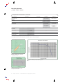
1
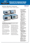
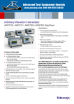
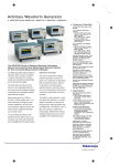
Data Timing Generator
DTG5078 • DTG5274 • DTG5334
Features & Benefits
Versatile Platform Combines
Features of Data Generator,
Pulse Generator and DC Source
Up to 3.35 Gb/s Data Rate
From 1 to 96 Data Channels
(Master/Slave)
Class Leading Delay Resolution
of 0.2 ps (DTG5274/DTG5334),
1 ps (DTG5078), Up to 600 ns
of Total Delay
Advanced Control Over Signal
Parameters to Meet Most Current
Testing Needs, Including Stressed
Eye Generation
– External Jitter Injection
(DTGM31, DTGM32 Modules)
– Level Control with 5 mV
Resolution
Easy to Use and Learn Shortens
Time to Test
New serial data standards, expanding
networks and ubiquitous computing
continually redefine the cutting-edge
of technology. The design engineer is
challenged to economize without sacrificing performance.
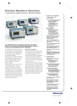
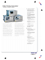
The DTG5000 Series combines the
power of a data generator with the capabilities of a pulse generator in a versatile,
bench-top form factor, shortening the
duration of complex test procedures and
simplifying the generation of low-jitter,
high-accuracy clock signals, parallel or
serial data across multiple channels. Its
modular platform allows you to easily
configure the performance of the instrument to your existing and emerging
needs to minimize equipment costs.
Three mainframes and five plug-in output
modules combine to cover a range of
applications from legacy devices to the
latest technologies. In addition, eight
low-current, independently-controlled DC
outputs can substitute for external power
supplies. Each mainframe incorporates
a full compliment of auxiliary input and
output channels to easily integrate with
other instruments, such as oscilloscopes
and logic analyzers, to create a flexible
and powerful lab.
– Easily Configure with Plug-in
Modules
– Intuitive Windows User
Interface
– Benchtop Form Factor
Up to 64 Mb Pattern Depth
Per Channel for Complex
Data Patterns
Applications
Semiconductor Device Functional
Test and Characterization
– Support for Semiconductor
Technologies from TTL
to LVDS
Compliance and Interoperability
Testing to Emerging Standards
–
–
–
–
–
PCI-Express
Serial ATA/2
InfiniBand
XAUI
HDMI/DVI
Magnetic and Optical
Storage Design
– Research, Development
and Test of Next-generation
Devices (HDD, DC/DVD,
Blue-ray)
Data Conversion Device Design
– Characterization and Test
of Next-generation D/A
Convertors
Jitter Transfer and Jitter
Tolerance Testing
Data Timing Generator
DTG5078 • DTG5274 • DTG5334
Characteristics
Mainframe Characteristics
Basic Features
Platform –
Benchtop mainframe with cold swappable plug-andplay plug-in output modules. Mainframes accept any
combination of output modules.
Number of Slots for Output Modules –
DTG5078: 8 slots (A, B, C, D, E, F, G, H).
DTG5274: 4 slots (A, B, C, D).
New DTG5334: 4 slots (A, B, C, D).
Master-Slave Capabilities –
DTG5078: Up to three DTG5078 mainframes can
be connected in Master-Slave configuration.
DTG5274: Up to two DTG5274 mainframes can
be connected in Master-Slave configuration.
DTG5334: Up to two DTG5334 mainframes can
be connected in Master-Slave configuration.
Operating Modes –
Pulse Generator Mode (slots A to D only).
Data Generator Mode.
Output Patterns –
NRZ, RZ, R1, Pulse patterns (DTG5078/5274/5334:
Slot A-D; DTG5078 Slot E-H, NRZ only).
Timing Parameters
Data Rate Range –
DTG5078:
NRZ: 50 Kb/s to 750 Mb/s.
RZ, R1, Pulse Mode: 50 Kb/s to 375 Mb/s.
DTG5274:
NRZ: 50 Kb/s to 2.7 Gb/s.
RZ, R1, Pulse Mode: 50 Kb/s to 1.35 Gb/s.
DTG5334:
NRZ: 50 Kb/s to 3.35 Gb/s
RZ, R1, Pulse Mode: 50 Kb/s to 1.675 Gb/s
Data Rate (Setting) Resolution –
Internal Clock: 8 digits.
External Clock: 4 digits.
External Phase Lock In: 4 digits.
2
Output Timing Controls
Delay Range –
PG Mode: 0 to 3 µs.
DG Mode:
Long Delay Off: 0 to 5 ns (NRZ, RZ, R1).
Long Delay On: NRZ:
Period ≥1.25 ns: 0 to 300 ns (Hardware sequence)
or to 600 ns (Software sequence).
Period <1.25 ns: 0 to (240 ns x period)
(Hardware sequence) or to (480 ns x period)
(Software sequence).
Long Delay On: RZ/R1:
Period ≥2.5 ns: 0 to 300 ns (Hardware sequence)
or to 600 ns (Software sequence).
Period <2.5 ns: 0 to (120 ns x period)
(Hardware sequence) or to (240 ns x period)
(Software sequence).
Delay Resolution –
DTG5078: 1 ps.
DTG5274/DTG5334: 0.2 ps.
Phase Resolution – 0.1%.
Differential Timing Offset Feature (between pair
of two adjacent channels [Odd and Even]) –
Range: –1.0 to 1.0 ns.
Resolution:
DTG5078: 1 ps.
DTG5274/DTG5334: 0.2 ps.
Semiautomatic Deskew Calibration –
Range: 500 ps.
Accuracy (after skew calibration):
100 ps, slots A to D.
200 ps, slots E to H (DTG5078 only).
Duty Cycle Adjustment Range –
0 to 100% (with 0 delay setting, RZ, R1, Pulse
mode only).
Duty Cycle Adjustment Resolution – 0.1%.
Pulse Width Maximum Range –
290 ps to (period –290 ps) (RZ, R1, Pulse
mode only).
(Range also depends on delay settings.)
Pulse Width Resolution – 5 ps.
Signal Sources • www.tektronix.com/signal_sources
Jitter Performance
(Output Channels)
Clock Pattern (“1010 ...” Clock Pattern)
Random Jitter –
DTG5078: <4 psRMS (at 750 Mb/s with DTGM21,
0.8 Vpk-pk, delay: 0.0 ns).
DTG5274: <3 psRMS (at 2.7 Gb/s with DTGM30,
0.8 Vpk-pk, delay: 0.0 ns).
DTG5334: <3 psRMS (at 3.35 Gb/s with DTGM30,
0.8 Vpk-pk, delay: 0.0 ns).
Data Pattern (PRBS pattern 215-1)
Total Jitter –
DTG5078: at 750 Mb/s
<18 psRMS, <85 pspk-pk (typical) with DTGM21,
0.8 Vpk-pk, delay: 0.0 ns).
DTG5274: at 2.7 Gb/s
<16 psRMS, <60 pspk-pk (typical) with DTGM30,
0.8 Vpk-pk, delay: 0.0 ns).
<14 psRMS, <60 pspk-pk (typical) with DTGM31,
0.8 Vpk-pk, delay: 0.0 ns).
DTG5334: at 3.35 Gb/s.
<13 psRMS, 50 pspk-pk (typical) with DTGM30 and
DTGM31, 0.8 Vpk-pk, delay: 0.0 ns).
Signal Control Features
Cross-point Adjustment (Duty Cycle Distortion) –
Range: 30% to 70%.
Resolution: 2%.
(Slots A to D, and DTGM30/DTGM31/DTGM32 used
in NRZ mode.)
Jitter Generation –
Jitter All or Partial Pattern.
Jitter Profile: Sine, Gaussian Noise, Square, Triangle.
Jitter Freq./Res.: 0.015 Hz to 1.56 MHz/1 mHz.
Jitter Amplitude: Up to 16.5 UIpk-pk (depending on data
rate and jitter frequency).
(Internal Jitter Generation available on Channel
A1 only.)
Data Timing Generator
DTG5078 • DTG5274 • DTG5334
Maximum Number of Output Channels
DTGM21
DTG5078*1
DTGM30
1
32
16
3
8
8
2
64
32
6
16
16
8
3
96
48
9
—
—
—
Number of Like
Mainframes
*1
DTGM31
DTGM32
DTGM21
DTG5274, DTG5334*1
DTGM30
DTGM31
DTGM32
4
The DTG5078 has a limit to the number of modules that may be installed; the total must be less than 100. The coefficient for each module is shown below.
DTGM30: 8, DTGM21: 10, DTGM31: 33, DTGM32: 32.
Pulse and Data Features
Pulse Generator (PG) Features (Unique to
PG Mode) –
Continuous or Burst.
Burst Count: 1 to 65,536.
Pulse Rate: Off, 1/1, 1/2, 1/4, 1/8, 1/16.
PRBS/PRWS Data Patterns –
(Note: Memory supports PRBS/PRWS patterns
and user can create errored PRBS.)
25–1, 26–1, 27–1, 28–1, 29–1, 210–1, 211–1,
212–1, 213–1, 214–1, 215–1, 223–1.
Sequencer Features
Data Patterns
Pattern Length per Channel (Pattern Memory) –
Minimum:
DTG5078: 1 bit (software mode) or 240 bits (hardware mode).
DTG5274 / DTG5334: 1 bit (software mode) or 960
bits (hardware mode).
Maximum:
DTG5078: 8,000,000 bits.
DTG5274: 32,000,000 bits (in multiples of four).
DTG5334: 64,000,000 bits (in multiples of four).
Built-in Data Patterns –
Binary Counter, Johnson Counter, Graycode Counter,
Walking Ones, Walking Zeros, Checker Board, User
Defined Patterns.
Pattern Import Capability –
Type/Tools:
Tektronix TLA Data Exchange Format File (*.txt).
Tektronix HFS Vector File (ASCII) (*.vca).
Tektronix HFS Vector File (binary) (*.vcb).
Tektronix AWG2000 Series (*.wfm).
Tektronix AWG400s/500s/610/710/710B (*.pat).
Tektronix DG2000 Series (*.dat).
Medium/Pass:
Sequence Length –
1 to 8,000 steps for main sequence.
1 to 256 steps for sub-sequence.
Max. Number of Blocks – 8,000.
Max. Number of Sub-Sequences – 50.
Repeat Counter – 1 to 65,536 or infinite.
Channel Addition – AND or XOR (slots A to D only).
Note: DTG5078 slots E, F, G and H do not support
the following: RZ, R1, pulse generation modes which
includes controls for trail delay/duty cycle/pulse
width, channel addition and variable cross-points.
Auxiliary Channels
Clock Out
Connector –
Complementary output (common offset and ground).
DTG5078/DTG5274: SMA rear panel.
DTG5334: SMA front panel.
Frequency Range –
DTG5078: 50 kHz to 750 MHz.
DTG5274: 50 kHz to 2.7 GHz.
DTG5334: 50 kHz to 3.35 GHz.
Frequency Resolution –
8 digit setting resolution.
Minimum: 1 mHz (e.g. with 50,000.000 Hz setting).
Internal Clock Accuracy – Within ±1 ppm.
Jitter –
DTG5078: <2 psRMS at 750 Mb/s, at 0.8 Vpk-pk (typical).
DTG5274: <2 psRMS at 2.7 Gb/s, at 0.8 Vpk-pk (typical).
DTG5334: <2 psRMS at 3.35 Gb/s, at 0.8 Vpk-pk (typical).
Amplitude/Resolution –
0.03 Vpk-pk to 1.25 Vpk-pk/10 mV (50 Ω).
0.06 Vpk-pk to 2.5 Vpk-pk/10 mV (1 MΩ).
Output Voltage Window –
–2.0 to 2.47 V (50 Ω).
–2.0 to 7.00 V (1 MΩ).
Max. Output Current – ±80 mA.
Transition Times (20% to 80%) –
DTG5078:
<85 ps (Amplitude = 0.1 Vpk-pk, Offset = 0 V) (typical).
<100 ps (Amplitude = 1.0 Vpk-pk, Offset = 0 V) (typical).
DTG5274:
<70 ps (Amplitude = 0.1 Vpk-pk, Offset = 0 V) (typical).
<80 ps (Amplitude = 1.0 Vpk-pk, Offset = 0 V) (typical).
DTG5334:
<100 ps (Amplitude = 1.0 Vpk-pk, Offset = 0 V) (typical).
Overshoot –
<10%, at High = 1.0 V, Low = 0 V into (50 Ω) (typical).
Import data via GPIB, LAN, CD-ROM, floppy drive,
USB memory devices.
Pattern Copy and Paste Capability –
Copy, paste, and rotation between data listing/
waveform editor and spreadsheet software
(e.g. Excel) via clipboard.
Signal Sources • www.tektronix.com/signal_sources
3
Data Timing Generator
DTG5078 • DTG5274 • DTG5334
Other Output Channels
Auxiliary DC Outputs –
–3.0 to 5.0 V/10 mV, Max. current: ±30 mA,
8 independently controlled outputs, Connector: 2 x 8
pin header on front panel.
Sync Out –
CML (current mode logic), VOH: 0 V , VOL: –0.4 V
(50 Ω) (typical), SMA Connector, SE, Front panel,
Rise/Fall Time (20 to 80%): 140 ps, Delay to Data
Out: –4.5 ns (typical).
10 MHz Reference Out –
1.2 Vpk-pk (50 Ω, AC coupled) (typical), 2.4 Vpk-pk
(1 MΩ, AC coupled) (typical), BNC Connector,
Rear Panel.
Environmental
Temperature
Humidity
Operating
Non-operating
+10 ºC to +40 ºC
-20 ºC to +60 ºC
20% to 80% relative humidity with
(no diskette in floppy drive):
a maximum wet bulb temperature 5% to 90% relative humidity with
of 29.4 ºC, non-condensing
a maximum wet bulb temperature
of 40 ºC, non-condensing
Altitude
Random Vibration
3,000 m (10,000 ft.)
12,000 m (40,000 ft.)
2.65 m/s2 RMS (0.27 GRMS),
from 5 Hz to 500 Hz, 10 minutes
22.36 m/s2RMS (2.28 GRMS) total
from 5 Hz to 500 Hz,
10 minutes each axis 3-axes.
30 minutes total
Input Channels
External Clock In –
Input Ranges:
DTG5078: 1 MHz to 750 MHz. SMA Connector,
Rear Panel.
DTG5274: 1 MHz to 2.7 GHz. SMA Connector,
Rear Panel.
DTG5334: 1 MHz to 3.35 GHz. SMA Connector,
Front Panel.
0.4 Vpk-pk to 2 Vpk-pk (50 Ω, AC Coupled), 50% ±5%
duty cycle.
10 MHz Reference In –
Input Ranges:
10 MHz ±0.1 MHz, 0.2 Vpk-pk to 3 Vpk-pk (50 Ω,
AC coupled), BNC Connector, Rear Panel.
Phase Lock In –
Input Ranges:
1 MHz to 200 MHz, 0.2 Vpk-pk to 3 Vpk-pk (50 Ω,
AC coupled), BNC Connector, Rear Panel.
Skew Cal In –
Single-ended, ECL (into 50 Ω to –2 V), SMA
Connector, Front Panel.
Trigger In –
Input Ranges:
–5 V to 5 V (50 Ω), 0.1 V resolution, –10 V to
10 V (1 kΩ), Min. 0.5 Vpk-pk (50 Ω), 1.0 Vpk-pk (1 kΩ),
Min. 20 ns pulse width, Positive or Negative edge
trigger, Delay timing: See manuals, BNC Connector,
Front Panel.
Event In –
Input Ranges:
–5 V to 5 V (50 Ω), 0.1 V resolution, –10 V to 10 V
(1 kΩ), 0.1 V resolution, Min. 0.5 Vpk-pk (50 Ω),
1.0 Vpk-pk (1 kΩ), Polarity: Normal or Invert, Delay
timing: See manuals, BNC Connector, Front Panel.
Instrument Control/Data
Transfer Ports
GPIB –
GPIB for remote control and data transfer. (Conforms
to IEEE 488.1, compatible with IEEE 488.2 and
SCPI-1999.0).
LAN –
LAN for PC interface, remote control and data
transfer (conforms to IEEE 802.3).
4
Computer System
and Peripherals
CompactPCI based PC, Celeron 566 MHz CPU,
Microsoft Windows 2000 Professional, 128 MB
SDRAM, 20 GB Hard Drive, 1.44 MB floppy drive
on front panel, CD-ROM in rear panel, included
USB compact keyboard and mouse.
PC I/O Ports
USB 1.1 compliant ports (3 total, 1 front, 2 rear),
PS/2 mouse and keyboard connectors (rear panel),
RJ-45 Ethernet connector (rear panel) supports
10Base-T and 100Base-Tx, VGA Out (rear panel),
RS-232C.
Physical Characteristics
Signal Sources • www.tektronix.com/signal_sources
Top and Bottom – 2 cm.
Side – 15 cm.
Rear – 7.5 cm.
Power Supply
Power Source – 100 to 240 VAC, 47 to 63 Hz.
Power Consumption – 560 W.
Safety –
UL61010B-1.
CAN/CSA-22.2 No. 1010.1.
EN61010-1/A2 1995.
Electromagnetic Compatibility (EMC) –
Europe:
EN61326 Class A.
EN61000-3-2, EN61000-3-3.
Display Characteristics –
LCD color display, 800 (H) x 600 (V) (SVGA).
Mainframe
Dimensions
Height
Width
Length
Output Module
Dimensions
Height
Width
Length
Weight (approx.)
DTG5078
DTG5274
DTG5334
DTGM21
DTGM30
DTGM31
DTGM32
Mechanical Cooling – Required
Clearance
Australia/New Zealand:
AS/NZS 2064.
mm
266
445
462
in.
10.5
17.5
19.7
mm
33
84
133
kg
17.5
17.0
17.0
0.26
0.27
0.27
0.27
in.
1.3
3.3
5.2
lbs.
38.6
37.5
37.5
0.57
0.60
0.60
0.60
Data Timing Generator
DTG5078 • DTG5274 • DTG5334
Output Module Characteristics
Basic Features
Output Channels
and Connections
Maximum Data Rate
(Calculated by
Transition Time)
DTGM21
DTGM30
4 single-ended (installed in DTG5078)
2 single-ended (DTG5274 / DTG5334)
4 SMA connectors
2 complementary
channels
4 SMA connectors
700 Mb/s
Normal/Complement
(Invert)
Source Impedance
50 Ω
1.1 Gb/s
DTGM31
DTGM32
1 complementary channel
2 SMA connectors
350 Mb/s*1
3.35 Gb/s
Selectable
—
50 Ω/23 Ω (selectable)
50 Ω
Enable/Disable
—
Yes (software switch)
Output Channel Timing
Transition Times (20%
to 80%) (50 Ω)
Transition Time Control
<540 ps (VOL = 0.0,
VOH = 1.0) (typical)
<340 ps (VOL = 0.0,
VOH = 1.0) (typical)
<1.5 ns (VOL = –1.0,
VOH = 2.0) (typical)
<1.0 ns (VOL = –1.65,
VOH = 3.7) (typical)
<95 ps (VOL = 0.0, VOH = 0.1) (typical)
<110 ps (VOL = 0.0, VOH = 1.0) (typical)
Yes
No
Slew Rate Control
Range
0.65 V/ns to 1.3 V/ns
into 50 Ω
—
Setting Resolution
0.01 V/ns
—
Channel Output Levels
Amplitude/ Resolution
0.25 to 3.5 Vpk-pk/5 mV
(into 50 Ω)
0.50 to 10.0 Vpk-pk/5 mV
(into 1 MΩ)
0.25 to 5.35 Vpk-pk/5 mV
(from 23 Ω source
impedance into 50 Ω)
0.03 to 1.25 Vpk-pk/5 mV (into 50 Ω)*2
0.06 to 2.5 Vpk-pk/5 mV (into 1 MΩ)*2
0.25 to 3.9 Vpk-pk/ 5 mV
(from 50 Ω source
impedance into 50 Ω)
0.50 to 7.8 Vpk-pk/ 5 mV
(from 50 Ω source
impedance into 1 MΩ)
Output Voltage Window
–1.5 V to 2.0 V (into 50 Ω)
–3.0 V to 7.0 V (into 1 MΩ)
–1.65 V to 3.70 V
(from 23 Ω source
impedance into 50 Ω)
–2.0 V to 2.47 V (into 50 Ω)
–2.0 V to 7.0 V (into 1 MΩ)
–1.2 V to 2.7 V
(from 50 Ω source
impedance into 50 Ω)
–2.4 V to 5.4 V
(from 50 Ω source
impedance into 1 MΩ)
DC Accuracy
(±3% of the set value) ±50 mV into 50 Ω to GND
Limit Setting
Maximum Output Current
Overshoot
Typical Support
Native Logic
External Jitter Control
*1
High and low level limits can be set
±40 mA
±80 mA
<16% (typical) at
High = 1.0 V, Low = 0 V
<15% (typical) at
High = 1.0 V, Low = 0 V
<10% (typical) at High = 1.0 V, Low = 0 V
TTL, CMOS
TTL, CMOS, (P)ECL,
LVPECL
LVDS, CMOS, (P)ECL, LVPECL, CML
No
Yes
Minimum pulse width >2.86 ns.
*2 Maximum output amplitude is dependent on output voltage window (offset). (See Figure 1, next page.)
Signal Sources • www.tektronix.com/signal_sources
5
Data Timing Generator
DTG5078 • DTG5274 • DTG5334
Output Module Characteristics (continued)
Basic Features
DTGM21
DTGM30
External Jitter Control
Input Channels and
Connectors
Input Range
DTGM31
DTGM32
1 single-ended channel
1 SMA connector
2 single-ended channels
2 SMA connectors
–0.5 V to +0.5 V (typical)
Max input: –1.0 V to +1.0 V
–0.5 V to +0.5 V
Jitter Frequency
DC to 250 MHz*3
DC to 50 MHz
Jitter Amplitude
240 pspk-pk for 1 Vpk-pk
input at Data rate
≤2.7 Gb/s*4
Range 1: Up to 1 ns
at 1 Vpk-pk
Range 2: Up to 2 ns
at 1 Vpk-pk
External Tri-state
(Hi Z) Control
No
Yes (SMB input connector)
No
Tri-state Enable
—
Enable: Hi 3.3 V, disable
Lo: 0.0 V
—
Control Channels
—
By output module level
—
Delay Time from Inhibit
In to Data Output
—
Active to Inhibit: 13 ns,
Inhibit to Active: 12 ns
—
*3 up to 400 MHz by overdriving jitter input (max –1.0 V to +1.0 Vpk-pk). (See Figure 2.)
*4 Jitter amplitude at data rates >2.7 Gb/s calculated as {240 – 61.5 x (data rate – 2.7)} pspk-pk for 1 Vpk-pk input. (See Figure 3.)
Figure 1. DTGM30, M31, M32 Output
Amplitude vs. Offset.
Figure 2. DTGM31 Jitter Input Frequency Response.
Figure 3. DTGM31 Maximum Jitter
Amplitude vs. Data Rate.
6
Signal Sources • www.tektronix.com/signal_sources
Data Timing Generator
DTG5078 • DTG5274 • DTG5334
Ordering Information
Mainframes
Cables
DTG5078
Type
750 Mb/s, 8-slot mainframe.
Lead set for DC Output, 16-CON, twisted pair, 24 in (60 cm)
012-A229-00
Pin header cable, 20 in. (51 cm)
012-1505-00
Pin header SMB cable, 20 in. (51 cm)
012-1503-00
DTG5274
2.7 Gb/s, 4-slot mainframe.
DTG5334
3.35 Gb/s, 4-slot mainframe.
Mainframes Include: Microsoft Windows 2000
Professional operating system recovery disk,
DTG5000 Series application software install disk,
user manual (volumes I and II), programmers
manual, technical reference, registration card,
accessory pouch, front cover, compact USB
keyboard, USB mouse, lead set for DC Output,
16-CON, twisted pair, 24 in. (60 cm), 50 Ω SMA
terminator (male, DC to 18 GHz), SMA connector
cap (10 ea. with DTG5078, 8 ea. with DTG5274/
DTG5334), power cord, calibration certificate.
Please specify power cord and language option
when ordering.
Part Number
GPIB Cable, double-shielded, 79 in (200 cm)
012-0991-00
Master/Slave Cable Set for Connecting Two Mainframes;
set of 4 SMA cables, 51 cm, 50 Ω (174-1427-00),
and set of 2 BNC cables, 46 cm (012-0076-00)
012-A230-00
Master/Slave Cable Set for Connecting Three Mainframes;
set of 6 SMA cables, 51 cm, 50 Ω (174-1427-00)
and set of 3 BNC cables, 46 cm (012-0076-00)
012-A231-00
BNC Cables 50 Ω
18 in. (46 cm)
012-0076-00
24 in. (61 cm)
012-1342-00
42 in. (107 cm)
012-0057-01
With Shield, 98 in. (250 cm)
012-1256-00
Mainframe Options
SMA Cables 50 Ω
Opt. 1R – Rackmount.
12 in (30 cm)
174-1364-00
20 in. (51 cm)
174-1427-00
39 in. (100 cm)
174-1341-00
60 in. (152 cm)
174-1428-00
International Power Plugs
Opt. A0 – North America power.
Opt. A1 – Universal EURO power.
Opt. A2 – United Kingdom power.
Opt. A3 – Australia power.
Opt. A5 – Switzerland power.
Opt. A6 – Japan power.
Opt. A10 – China power.
Opt. A99 – No power cord or AC adapter.
Delay SMA Cables 50 Ω
1 ns (male to female)
015-1019-00
2 ns
015-0560-00
2 ns (male to female)
015-1005-00
5 ns
015-0561-00
5 ns (male to female)
015-1006-00
Language Options
Opt. L0 – English.
Opt. L5 – Japanese.
Adapters and Connectors
Output Modules
Type
DTGM21
Part Number
SMB to BNC Adapter
015-0671-00
50 Ω SMA (male) to BNC (female) Adapter
015-0554-00
50 Ω SMA (female) to BNC (male) Adapter
015-0572-00
50 Ω N (male) to SMA (male) Adapter
015-0369-00
50 Ω SMA Adapter (male to female), DC to 18 GHz, VSWR: 1.2
015-0549-00
50 Ω SMA Adapter (slide on type female to male),
DC to 18 GHz, VSWR: 1.05 + 0.002F (GHz)
015-0553-00
DTGM30
50 Ω SMA T-Connector (male to female/female)
015-1016-00
2 channels.
1.25 Vpk-pk (50 Ω), 2.5 Vpk-pk (1 MΩ).
Tr/Tf (20% to 80%) <110 ps (1 Vpk-pk, into
50 Ω), fixed.
50 Ω SMA Divider (female/female/female), 6 dB,
DC to 18 GHz, VSWR: 1.9
015-0565-00
4 channels (DTG5078), 2 channels
(DTG5274/DTG5334).
5.35 Vpk-pk (from 23 Ω to 50 Ω).
3.9 Vpk-pk (50 Ω), 7.8 Vpk-pk (1 MΩ).
Tr/Tf (20% to 80%) <340 ps (1 Vpk-pk, into
50 Ω), fixed.
External Tri-state (Hi_Z) control function.
Signal Sources • www.tektronix.com/signal_sources
7
Data Timing Generator
Contact Tektronix:
ASEAN / Australasia (65) 6356 3900
DTG5078 • DTG5274 • DTG5334
Austria +41 52 675 3777
Balkan, Israel, South Africa and other ISE Countries +41 52 675 3777
Belgium 07 81 60166
DTGM31
1 channel.
1.25 Vpk-pk (50 Ω), 2.5 Vpk-pk (1 MΩ).
Tr/Tf (20% to 80%) <110 ps (1 Vp-p, into
50 Ω), fixed.
External jitter control input.
Jitter frequency DC – 400 MHz.
Jitter amplitude up to 240 ps.
DTGM32
1 channel.
1.25 Vpk-pk (50 Ω), 2.5 Vpk-pk (1 MΩ).
Tr/Tf (20% to 80%) <110 ps (1 Vpk-pk, into
50 Ω), fixed.
2 ch external jitter control input.
Jitter frequency DC – 50 MHz.
Jitter amplitude up to 1 ns/2 ns.
Output Modules Include: Installation sheet
(Japanese/English), SMA connector cap (set of 4
with DTGM21, set of 2 with DTGM30), 50 Ω SMA
terminator (DC to 18 GHz) (set of 2 with DTGM30,
set of 1 with DTGM31/32), registration card.
Service Options
Opt. C3 – Calibration Service 3 years.
Opt. C5 – Calibration Service 5 years.
Opt. D1 – Calibration Data Report (English).
Opt. D3 – Calibration Data Report 3 years
(with Opt. C3).
Opt. D5 – Calibration Data Report 5 years
(with Opt. C5).
Opt. R3 – Repair Service 3 years.
Opt. R5 – Repair Service 5 years.
Brazil & South America 55 (11) 3741-8360
Recommended
Accessories
Service Manual (English) – Order
071-1285-xx.
Transition Time Converters – Output
transition time (10% to 90%).
150 ps – Order 015-0710-00.
250 ps – Order 015-0711-00.
500 ps – Order 015-0712-00.
1000 ps – Order 015-0713-00.
2000 ps – Order 015-0714-00.
Canada 1 (800) 661-5625
Central East Europe, Ukraine and the Baltics +41 52 675 3777
Central Europe & Greece +41 52 675 3777
Denmark +45 80 88 1401
Finland +41 52 675 3777
France & North Africa +33 (0) 1 69 86 81 81
Germany +49 (221) 94 77 400
Hong Kong (852) 2585-6688
India (91) 80-22275577
Italy +39 (02) 25086 1
Japan 81 (3) 6714-3010
Test Adapters
HDMI TPA-R Test Adapter Set – HDMI
TPA-R TDR (set of 2), HDMI TPA-R DI
(differential), HDMI TPA-R SE (singleended). Order 013-A012-50.
HDMI TPA-P Test Adapter Set – HDMI
TPA-P TDR, HDMI TPA-P DI (differential),
HDMI TPA-P SE (single-ended). Order
013-A013-50.
DVI TPA-R Test Adapter Set– DVI TPA-R
TDR (set of 2), DVI TPA-R DI (differential),
DVI TPA-R SE (single-ended). Order
013-A014-50.
Note: These adapters do not include clock
recovery circuits.
Luxembourg +44 (0) 1344 392400
Mexico, Central America & Caribbean 52 (55) 56666-333
Middle East, Asia and North Africa +41 52 675 3777
The Netherlands 090 02 021797
Norway 800 16098
People’s Republic of China 86 (10) 6235 1230
Poland +41 52 675 3777
Portugal 80 08 12370
Republic of Korea 82 (2) 528-5299
Russia & CIS 7 095 775 1064
South Africa +27 11 254 8360
Spain (+34) 901 988 054
Sweden 020 08 80371
Switzerland +41 52 675 3777
Taiwan 886 (2) 2722-9622
United Kingdom & Eire +44 (0) 1344 392400
USA 1 (800) 426-2200
For other areas contact Tektronix, Inc. at: 1 (503) 627-7111
Updated 5 January 2006
Our most up-to-date product information is available at:
www.tektronix.com
Product(s) are manufactured in ISO registered facilities.
Product(s) complies with IEEE Standard 488.1-1987, RS-232-C, and with
Tektronix Standard Codes and Formats.
Copyright © 2006, Tektronix. All rights reserved. Tektronix products are covered
by U.S. and foreign patents, issued and pending. Information in this publication
supersedes that in all previously published material. Specification and price
change privileges reserved. TEKTRONIX and TEK are registered trademarks
of Tektronix, Inc. All other trade names referenced are the service marks,
trademarks or registered trademarks of their respective companies.
2/06
HB/WOW
86W-16679-4