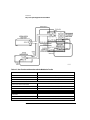
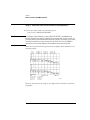
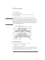
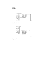
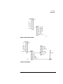
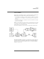
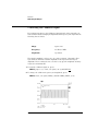
1
Agilent 71501D
Jitter Analysis System
User’s Guide
© Copyright
Agilent Technologies 2002 2003
All Rights Reserved. Reproduction, adaptation, or translation without prior written
permission is prohibited,
except as allowed under copyright laws.
Agilent Part No. 71501-90011
Printed in USA
September 2003
Agilent Technologies, Inc.
Digital Signal Analysis Operation
1400 Fountaingrove Parkway
Santa Rosa, CA 95403, USA
Warranty
The material contained in this
document is provided “as is,”
and is subject to being
changed, without notice, in
future editions. Further, to the
maximum extent permitted by
applicable law, Agilent disclaims all warranties, either
express or implied, with
regard to this manual and any
information contained herein,
including but not limited to
the implied warranties of merchantability and fitness for a
particular purpose. Agilent
shall not be liable for errors or
for incidental or consequential
damages in connection with
the furnishing, use, or performance of this document or of
any information contained
herein. Should Agilent and the
user have a separate written
agreement with warranty
terms covering the material in
this document that conflict
with these terms, the warranty terms in the separate
agreement shall control.
Restricted Rights Legend.
Use, duplication, or disclosure by the U.S. Government
is subject to restrictions as set
forth in subparagraph (c) (1)
(ii) of the Rights in Technical
Data and Computer Software
clause at DFARS 252.227-7013
ii
for DOD agencies, and subparagraphs (c) (1) and (c) (2)
of the Commercial Computer
Software Restricted Rights
clause at FAR 52.227-19 for
other agencies.
Exclusive Remedies.
The remedies provided herein
are buyer's sole and exclusive
remedies. Agilent Technologies shall not be liable for any
direct, indirect, special, incidental, or consequential damages, whether based on
contract, tort, or any other
legal theory.
Safety Symbols.
CAUTION
The caution sign denotes a
hazard. It calls attention to a
procedure which, if not correctly performed or adhered
to, could result in damage to
or destruction of the product.
Do not proceed beyond a caution sign until the indicated
conditions are fully understood and met.
WARNING
The warning sign denotes a
hazard. It calls attention to a
procedure which, if not correctly performed or adhered
to, could result in injury or
loss of life. Do not proceed
beyond a warning sign until
the indicated conditions are
fully understood and met.
Contents
1 Introduction
Analysis with the Agilent 71501D 1-2
2 Installation
Introduction 2-2
Step 1. Inspect the Shipment 2-11
Step 2. Install N1015A (Optional) 2-12
Step 3. Set Up the Equipment with an N1015A 2-16
Step 3. Set Up the Equipment without an N1015A 2-30
Step 4. Set the MSIB and GPIB addresses 2-43
Step 5. Load the Personality 2-45
Step 6. Select Template and Measurement Conditions 2-49
To perform a system calibration 2-52
To rack mount the 71501D 2-54
To use two MMS displays 2-54
Returning the Instrument for Service 2-55
3 Tutorials
Tutorial 1: Jitter Transfer Measurements 3-3
Tutorial 2: Jitter Tolerance Measurements 3-17
Tutorial 3: Jitter Generation and Output 3-32
Tutorial 4: Diagnostic Measurements 3-39
Troubleshooting the Jitter Analyzer System 3-49
4 Reference
Menu Maps 4-3
Jitter Measurements 4-8
Analyzer System Configuration and Setup 4-17
Calibrating the Analyzer 4-27
Memory Cards, Disks, and RAM 4-38
Print or Plot Measurement Results 4-49
5 Programming
6 Specifications and Characteristics
70820A Input Channel Specifications 6-3
N1015A Specifications 6-4
Contents-1
Contents
Jitter Characteristics 6-6
Jitter Modulation Capabilities of 71501D System Configurations 6-9
Contents-2
1
Introduction
Introduction
Analysis with the Agilent 71501D
Analysis with the Agilent 71501D
The Agilent 71501D jitter analysis system provides advanced analysis of highspeed digital communication waveforms and the components which generate
them. The jitter analyzer configuration performs automatic compliance and
network equipment testing, to SONET, SDH, and custom standards. In addition, it can perform diagnostic measurements of the jitter spectrum and waveform.
The Agilent 71501D consists of the following:
•
•
•
•
•
•
•
Jitter analyzer personality
Microwave transition analyzer module (jitter receiver/controller)
Color display/mainframe
Jitter modulation source
Clock source
Modulation test set
User’s guide
You will also need a pattern generator for all of the jitter applications and an
error detector for the jitter tolerance application. The 71501D jitter analysis
system can share the 70004A color display with a compatible modular pattern
generator and an error detector. The compatible sources have different frequency ranges and FM characteristics. Refer to “Jitter System Configurations”
on page 2-2 for a list of possible system equipment. Also refer to Chapter 6,
“Specifications and Characteristics” for detailed information.
1-2
Introduction
Analysis with the Agilent 71501D
Menu and Softkey Overview
Most front-panel controls are accessed through softkey menus. Softkeys are
the seven buttons located on each side of the 70004A screen. The functions of
softkeys change according to the menus displayed on the screen. Use the leftside softkeys to access the major menus.
Use the following three front-panel keys on the 70004A display to select the
available softkey menus:
USER
press to select between the jitter measurement personality and
Instrument BASIC menus. (The 71501D jitter analysis personality
must first be loaded as described in Chapter 2, “Installation”).
MENU
press to view menus for the 70820A microwave transition analyzer
module. Refer to “Menu Maps” on page 4-3 to learn how to view
the pattern generator’s menus.
DISPLAY
press to view the menus for the 70004A display.
1-3
Introduction
Analysis with the Agilent 71501D
• A softkey with ON and OFF in its label can be used to turn the softkey’s function on or off. To turn the function on, press the softkey so ON is underlined.
To turn the function off, press the softkey so OFF is underlined. For example,
an ON or OFF softkey function for MUX/DMUXwill be indicated in this manual
as: MUX/DMUX ON.
• A softkey such as ERRORS BER offers you a choice of functions. In this case, you
could choose to count the number of errors by pressing the softkey until ERRORS is
underlined, or determine the bit error rate by pressing the softkey until BER is underlined. For example, ERRORS BER BER.
• When some softkeys, such as DELAY, are pressed the first time, only the function
will be highlighted, as shown in the graphic below.The display’s active function
area shows the value of any activated function. To change the value of the function, use the numeric keys, step keys, or knob. When entering a value using the numeric keys, the entry must be terminated by pressing either one of the units keys, such
as MHz, or if no units are required, the ENTER key. When adjusting the value using
the step keys or knob, the units are entered automatically by the analyzer. When you
are finished entering the value, press the softkey again to highlight the on and off
functions. Pressing the HOLD key deactivates the active function. Pressing the
HOLD key a second time blanks the right-side softkeys. Use the ← (backspace) key
to backspace over numbers entered using the data-entry keypad.
Analyzer’s Setup Menu
1-4
Introduction
Analysis with the Agilent 71501D
Jitter Analysis with the 71501D
NOTE
The jitter personality must first be loaded as described in Chapter 2, “Installation”.
The jitter analyzer can be operated in the following modes:
Jitter Transfer
Mode
Displays a jitter transfer plot or list of the measured output jitter of the deviceunder-test divided by the input jitter versus the jitter frequency.
1-5
Introduction
Analysis with the Agilent 71501D
Jitter Tolerance
Mode
Displays the error performance in the presence of specified levels of jitter in
plot or list form.
Jitter Output and
Generation Mode
Displays results of peak-to-peak and RMS intrinsic jitter measurements.
Diagnostic
Measurement
Mode
Displays the spectrum and waveform of the clock signal or of the demodulated
jitter signal, extracted from the jittered clock signal. Use this mode as an aid to
solve jitter-related problems.
1-6
Introduction
Analysis with the Agilent 71501D
1-7
Introduction
Analysis with the Agilent 71501D
1-8
2
Installation
Installation
Introduction
Introduction
In this chapter, you’ll install the hardware and software and begin to learn
about the measurement process. For more detailed procedures on the specific
measurement applications, refer to Chapter 3, “Tutorials”.
Chapter Contents Introduction 2-2
Jitter System Configurations 2-2
Clock Source Considerations 2-3
Optional N1015A Modulation Test 2-3
Supported Instrument, Cables, and Accessories 2-7
Step 1. Inspect the Shipment 2-11
Step 2. Install N1015A (Optional) 2-12
Step 3. Set Up the Equipment with an N1015A 2-16
Step 3. Set Up the Equipment without an N1015A 2-30
Step 4. Set the MSIB and GPIB addresses 2-43
Step 5. Load the Personality 2-45
Step 6. Select Template and Measurement Conditions 2-49
To perform a system calibration 2-52
To use two MMS displays 2-54
To rack mount the 71501D 2-54
Returning the Instrument for Service 2-55
Jitter System Configurations
NOTE
For specifications and installation cautions and warnings on all instruments in the system,
except for the N1015A, refer to the individual instrument manuals.
The Agilent 71500A and Agilent 70820A products have been designed and
tested in accordance with the standards listed on the Manufacturer’s Declaration of Conformity, and has been supplied in a safe condition. This documentation contains information and warnings that must be followed by the user to
ensure safe operation and to maintain the product in a safe condition.
2-2
Installation
Introduction
WARNING
If this product is not used as specified, the protection provided by the equipment
could be impaired. This product must be used in a normal condition (in which all
means for protection are intact) only. Altitude up to 2000 Meters, temperature 0 to 40
°C.
CAUTION
Total input signal power to the 70820A module’s front-panel RF INPUT connectors must not
exceed +16 dBm. Because there is no RF input attenuator, power in excess of +16 dBm may
damage the instrument. The largest measurable power level before signal compression is +4
dBm.
There must be only one of the following instruments:
•
•
•
•
•
modulation source
microwave transition analyzer
pattern generator (optionally)
error detector (optionally)
N1015A modulation test set (optionally)
There must be at least one of the following instruments:
• display/mainframe
• clock source
The 71501D jitter analysis system may consist of the equipment shown in
Table 2-1, “Jitter System Configurations,” on page 2-7.
Clock Source Considerations
You can use either a modular or stand-alone clock source and error performance analyzer. Refer to Table 2-2, “Clock Source and Compatible Equipment,” on page 2-9.
Optional N1015A Modulation Test
The N1015A modulation test set adds the range of 2.4 to 3.2 GHz with 20 MHz
modulation (71501D options 300, 305) or 9.8 to 13 GHz with 80 MHz modulation (71501D options 310, 305).
2-3
Installation
Introduction
Front Panel
Figure 2-1 on page 2-4 shows the front-panel connectors and POWER ON
switch.
10 Gb/s and 2.5 Gb/s In: 3.5 mm input connectors for output RF signal from
the clock source. Use the provided 3.5 mm adapters on these connectors as
connector savers.
10 Gb/s and 2.5 Gb/s Out: 3.5 mm output connectors for signal to CLOCK IN
on the pattern generator. Use the provided 3.5 mm adapters on these connectors as connector savers.
Dut Out: 3.5 mm input connector for output signal of device under test. Use a
provided 3.5 mm adapter on this connector as connector savers.
Ch 1 MJA: 3.5 mm output connector to channel 1 on the microwave transition analyzer module. Use a provided 3.5 mm adapter on this connector as
connector savers.
Jitter Modulation In: BNC input connector for signal input from jitter modulation source.
Jitter Modulation Out: BNC output connector for FM input on a clock
source.
The front panel LEDs indicate the status of the N1015A. If the ERROR LED
lights at any time other than during self test, an error condition exists. The
other LEDs, RMT (remote), LSN (listen), TLK (talk), and SWITCHING indicate the normal functioning and do not indicate an error condition.
Figure 2-1. N1015A Front Panel
2-4
Installation
Introduction
Rear Panel
Figure 2-2 on page 2-5 shows the N1015A rear panel. The only rear-panel connector provided for the user is the GPIB port. The factory default setting of
the GPIB switch is 9 as shown in Figure 2-3 on page 2-5. The N1015A rearpanel power line module contains the line fuse as shown in Figure 2-4 on
page 2-6. If the fuse is bad, replace it with the spare fuse (Agilent part number
2110-1124)
.
Figure 2-2. N1015A Rear Panel
Figure 2-3. N1015A Rear Panel with GPIB address set to 9
2-5
Installation
Introduction
Figure 2-4. N1015A Power Line Module
2-6
Installation
Introduction
Supported Instrument, Cables, and Accessories
Table 2-1. Jitter System Configurations (1 of 2)
Microwave Transition Analyzer
Frequency Range
70820Aa microwave transition analyzer module: option UF3, expanded memory
DC–40 GHz
Display Mainframe
70004Aa color display and mainframe
Jitter Personality Carda
Jitter Modulation
Frequency Range
33250Aa function/arb waveform generator
80 MHz
3325A/B synthesizer/function generator (OBSOLETE)
20 MHz
3324A synthesizer/function generator (OBSOLETE)
20 MHz
Modulation Test Set
Frequency Range
N1015Aa
Option 300, 20 MHz modulator
Option 310, 80 MHz modulator
Option 305, 20 MHz and 80 MHz modulators
2.4–3.2 GHz
9.8–13 GHz
2.4–3.2 and 9.8–13 GHz
Clock Source
Frequency Range
E4422Bb RF signal generator
250 kHz–4 GHz
83752Aa synthesized microwave sweeper
10 MHz–20 GHz
83732B synthesized signal generator
10 MHz–20 GHz
70340A modular signal generator
1 GHz–20 GHz
83732A synthesized signal generator (OBSOLETE)
10 MHz–20 GHz
70311A Option H08 modular signal generator with modulation input (OBSOLETE)
16 MHz–3.1 GHz
Error Performance Analyzerc
Data Rate
2-7
Installation
Introduction
Table 2-1. Jitter System Configurations (2 of 2)
Stand alone models:
N4901A Serial BERT
50 MHz to 13.5 GHz
N4902A Serial BERT
50 MHz to 7 GHz
N4906A Smart BERT 3.6 Gb/s
50 Mb/s–3.6 Gb/s
86130A BitAlyzer error analyzer
50 Mb/s–3.6 Gb/s
Modular models:
70843C option UHF error performance analyzer (PART OF 71612C pattern generator and error
detector)
100 Mb/s–12.5 Gb/s
70843A/B option UHF error performance analyzer (OBSOLETE)) (PART OF 71612A/B pattern generator
and error detector)
100 Mb/s–12 Gb/s
71603A/B error performance analyzer(OBSOLETE)
70841A/B modular pattern generator (OBSOLETE)
70842A/B modular error detector (OBSOLETE)
100 Mb/s–3 Gb/s
a. Standard instrument for the 71501D jitter analysis system.
b. Recommended clock source for 3 Gb/s applications.
c. Instrument is not bundled with the 70501D jitter analysis system.
2-8
Installation
Introduction
Table 2-2. Clock Source and Compatible Equipment
Clock Source
Compatible Error Performance Instruments
E4422B RF signal generator
83752A microwave signal generator
83732A/B synthesized signal generator
N4906A Smart BERT 3.6 Gb/s
86130A BitAlyzer error performance analyzer
70843A/B/C option UHF error performance analyzer (component of 71612A/
B/C)
pattern generator
error detector
71603B error performance analyzer
70841A/B modular pattern generator
70842A/B modular error detector
71603B error performance analyzer
70841A/B modular pattern generator
70842A/B modular error detector
71603B error performance analyzer
70841A/B modular pattern generator
70842A/B modular error detector
70843A/B/C option UHF error performance analyzer (component of 71612A/
B/C)
pattern generator
error detector
70311A Option H08 signal generator
70340A modular synthesized signal generator
Clock Source
Compatible Jitter Modulation Instrument
E4422B RF signal generator
33250A function/arb waveform generator
2-9
Installation
Introduction
Table 2-3. Cables and Accessories for 71501D System Configurations
Cables:
SMA to SMA
BNC cable
Reference BNC to SMB cables
GPIB cables
Options and Part numbers
8120-4948
8120-2582
8120-5048
8120-3445
Miscellaneous:
3.5 mm (f) to 2.4 mm (f) (2)
6 dB attenuator
Bandpass Filter 155 Mb/s (2)
Bandpass Filter 622 Mb/s (2)
Low Pass Filter 800 MHz (2)
Low Pass Filter 1.5 GHz (2)
Bandpass Filter 2488 Mb/s (2)
Bandpass Filter 2666 Mb/s (2)
Low Pass Filter 4.0 GHz (2)
Bandpass Filter 9953 Mb/s (2)
Bandpass Filter 10.7092 Gb/s (2)
Bandpass Filter 12.4416 Gb/s (2)
Low Pass Filter 12.4 GHz (2)
Bandpass Filter 10.66423 Gb/s (2)
2-10
1250-2277
8493C
71501D Option 400 (0955-0969)
71501D Option 410 (0955-0732)
71501D Option 412 (0955-1465)
71501D Option 417 (0955-1464)
71501D Option 420 (0955-0731)
71501D Option 430 (0955-1468)
71501D Option 435 (0955-1466)
71501D Option 440 (0955-0970)
71501D Option 450 (0955-1469)
71501D Option 460 (0955-1467)
71501D Option 467 (0955-1394)
71501D Option 480 (0955-1470)
Installation
Step 1. Inspect the Shipment
Step 1. Inspect the Shipment
WARNING
Observe the notes, cautions, warnings, and installation procedures in the
documentation that was supplied with the individual instruments in the 71501D.
1 Inspect the shipping containers for damage.
2 Inspect the instruments.
3 Verify that you received the options and accessories you ordered.
In your 71501D system shipment there is a packing list that lists all of the
items included in the shipment. The accessory package contains many items
that you will need to configure the equipment. Pay particular attention to the
3.5mm (female) to 3.5 mm (female) connectors that you should put on the
optional N1015A modulation test set ports as connector savers.
NOTE
Keep the shipping container and cushioning material until you have inspected the contents of
the shipment for completeness and have checked the instrument mechanically and electrically.
If anything is missing or defective, contact your nearest Agilent Technologies
Sales Office. Refer to “Returning the Instrument for Service” on page 2-55. If
the shipment was damaged, contact the carrier, then contact the nearest
Agilent Sales Office. Keep the shipping materials for the carrier’s inspection.
The Agilent Sales Office will arrange for repair or replacement at Agilent’s
option without waiting for claim settlement.
4 Review the individual manuals for your equipment to ensure that your
operating or storage environment is suitable for the instruments. If you ordered
an N1015A Modulation Test Set, refer to “Step 2. Install N1015A (Optional)” on
page 2-12.
Install the instruments so that the detachable power cords are readily identifiable and is easily reached by the operator. The detachable power cord is the
instrument disconnecting device. It disconnects the mains circuits from the
mains supply before other parts of the instrument. The front panel switch is
only a standby switch and is not a LINE switch. Alternatively, an externally
installed switch or circuit breaker (which is readily identifiable and is easily
reached by the operator) may be used as a disconnecting device.
2-11
Installation
Step 2. Install N1015A (Optional)
Step 2. Install N1015A (Optional)
Observe the following notes, cautions, and warnings that apply to the N1015A.
This product has been designed and tested in accordance with the standards
listed in the Manufacturer’s Declaration of Conformity, and has been supplied
in a safe condition. The documentation contains information and warnings
which must be followed by the user to ensure safe operation and to maintain
the product in a safe condition.
WARNING
This is a Safety Class 1 Product (provided with a protective earthing ground
incorporated in the power cord). The mains plug shall only be inserted in a socket
outlet provided with a protective earth contact. Any interruption of the protective
conductor inside or outside of the instrument is likely to make the instrument
dangerous. Intentional interruption is prohibited.
WARNING
No operator serviceable parts inside. Refer servicing to qualified service personnel.
To prevent electrical shock do not remove covers.
WARNING
For continued protection against fire hazard, replace line fuse only with same type
and ratings (FUSE (METRIC) 3.15A 250V TD FE UL-REC, Agilent part number 21101124). The use of other fuses or materials is prohibited.
CAUTION
Always use the three-prong AC power cord supplied with this product. Failure to ensure
adequate earth grounding by not using this cord may cause product damage.
CAUTION
This product is designed for use in INSTALLATION CATEGORY II and POLLUTION DEGREE 2 per
IEC 61010-1 and 664 respectively.
CAUTION
Ventilation Requirements: When installing the product in a cabinet, the convection into and
out of the product must not be restricted. The ambient temperature (outside the cabinet) must
be less than the maximum operating temperature of the product by 4 °C for every 100 watts
dissipated in the cabinet. If the total power dissipated in the cabinet is greater than 800 watts,
then forced convection must be used.
2-12
Installation
Step 2. Install N1015A (Optional)
WARNING
If this product is not used as specified, the protection provided by the equipment
could be impaired. This product must be used in a normal condition (in which all
means for protection are intact) only.
WARNING
To prevent electrical shock, disconnect the Agilent Technologies model N1015A
from mains before cleaning. Use a dry cloth or one slightly dampened with water to
clean the external case parts. Do not attempt to clean internally.
Instrument
Markings
The instruction documentation symbol. The product is marked with this
warning symbol when it is necessary for the user to refer to the instructions in the manual.
The AC symbol is used to indicate the required nature of the line module input power.
The ON, STANDBY, OFF, Push Switch IN and Push
Switch OUT symbols. The ON and OFF symbols are
used to mark the functions associated with the positions of an instrument LINE switch. The On and STANDBY symbols are used
to mark the functions associated with the positions os an instrument POWER
switch. The Push Switch IN and Push Switch OUT symbols are used in conjunction with the ON and OFF or STANDBY symbols to mark the functions
associated with the position of a two-position push type LINE or POWER
switch.
ON, , OFF,
The CE mark is a registered trademark of the European Community.
The CSA mark is a registered trademark of the Canadian Standards
Association.
The C-Tick mark is a registered trademark of the Australian Spectrum
Management Agency.
ISM1-A
This text denotes the instrument is an Industrial Scientific and Medical
Group 1 Class A product.
Procedure
1 Verify that the line power meets the requirements listed in Table 2-4 on
page 2-14.
2 Connect the line-power cord to the N1015A’s rear-panel connector.
3 Connect the other end of the line-power cord to the power receptacle.
2-13
Installation
Step 2. Install N1015A (Optional)
Various power cables are available to connect the N1015A to ac power outlets
unique to specific geographic areas. The cable appropriate for the area to
which the N1015A is originally shipped is included with the unit. You can
order additional ac power cables for use in different geographic areas. Refer to
Table 2-6 on page 2-15.
Larry will get back to me on line power requirements! and two fuses?
Table 2-4. N1015A Line Power Requirements
Power:
115 VAC: 50 VA MAX. .
230 VAC: 70 VA MAX.
Voltage
nominal: 115 VAC / 230 VAC
range 115 VAC: 90–132 V
range 230 VAC: 198–254 V
Frequency
nominals: 50 Hz / 60 Hz
range: 47–63 Hz
Table 2-5. N1015A Environmental Specifications
Use
Temperature
Operating
Non-operating
Maximum Relative Humidity
Altitude
Operating
Non-operating
Weight
Dimensions
Height
Width
Depth
2-14
indoor
0°C to +55°C
–40°C to +70°C
80% for temperatures up to 31°C decreasing linearly to 50%
relative humidity at 40°C.
Up to 5,600 meters (15,000 ft)
Up to 5,600 meters (15,000 ft)
22 lbs (10 kgm)
88 mm
425 mm
498 mm
Installation
Step 2. Install N1015A (Optional)
Table 2-6. Available Line Cords
Plug Type
Cable Part No. Plug Description
Length
(in/cm)
Color
Country
250V
8120-1351
Straight *BS1363A
90/228
Gray
8120-1703
90°
90/228
Mint Gray
United Kingdom, Cyprus,
Nigeria, Zimbabwe,
Singapore
8120-1369
Straight *NZSS198/ASC
79/200
Gray
87/221
Mint Gray
250V
Australia, New Zealand
90°
8120-0696
250V
125V
250V
8120-1689
Straight *CEE7-Y11
79/200
Mint Gray
8120-1692
90°
79/200
Mint Gray
8120-2857p
Straight (Shielded)
79/200
Coco Brown
8120-1378
Straight *NEMA5-15P
90/228
Jade Gray
8120-1521
90°
90/228
Jade Gray
8120-1992
Straight (Medical) UL544
96/244
Black
8120-2104
Straight *SEV1011
79/200
Mint Gray
8120-2296
1959-24507
79/200
Mint Gray
East and West Europe,
Saudi Arabia, So. Africa,
India (unpolarized in many
nations)
United States, Canada,
Mexico, Philippines,
Taiwan
Switzerland
Type 12 90°
220V
250V
100V
8120-2956
Straight *DHCK107
79/200
Mint Gray
8120-2957
90°
79/200
Mint Gray
8120-4211
Straight SABS164
79/200
Jade Gray
8120-4600
90°
79/200
8120-4753
Straight MITI
90/230
8120-4754
90°
90/230
Denmark
Republic of South Africa
India
Dark Gray
Japan
* Part number shown for plug is the industry identifier for the plug only. Number shown for
cable is the Agilent Technologies part number for the complete cable including the plug.
2-15
Installation
Step 3. Set Up the Equipment with an N1015A
Step 3. Set Up the Equipment with an N1015A
If you do not plan to use an N1015A modulation test set with your system, skip
this step and continue with “Step 3. Set Up the Equipment without an
N1015A” on page 2-30. The N1015A modulation test set adds the range of 2.4
to 3.2 GHz with 20 MHz modulation (71501D options 300, 305) or 9.8 to 13
GHz with 80 MHz modulation (71501D options 310, 305).
• Connect the test equipment using the diagrams referred to in one of the following four setups:
Jitter Transfer and Generation Measurements
• Modular clock source and error performance analyzer. See Test Setup 2-1 on
page 2-17.
• Stand-alone clock source and error performance analyzer. See Test
Setup 2-2 on page 2-20.
Jitter Tolerance Measurements
• Modular clock source and error performance analyzer. See Test Setup 2-3 on
page 2-24.
• Stand-alone clock source and error performance analyzer. See Test
Setup 2-4 on page 2-27.
CAUTION
To prevent damage to the 70820A microwave transition analyzer, always have either a
bandpass filter or a dc block connected to the analyzer input channels.
CAUTION
To avoid damage, do not exceed +10 dBm input power or ±2 V DC to any N1015A front panel
RF inputs. Do not apply DC voltage exceeding ±10V to the N1015A Jitter Modulation Input.
CAUTION
The N1015A circuitry can be damaged by electrostatic discharge (ESD). Avoid applying static
discharge to the N1015A RF connectors and jitter modulation connectors.
CAUTION
All GPIB and MSIB connections must be made prior to turning on the system.
Connect the GPIB cables in any arrangement as long as all of the instruments
are interconnected.
Connect the MSIB cables to the instruments in a closed loop fashion. You can
install the MMS modules in multiple mainframe configurations.
2-16
Installation
Step 3. Set Up the Equipment with an N1015A
Test Setup 2-1. Jitter Transfer and Generation Connections with Modular Error Performance Analyzer and Modular Clock Source
The 70841A/B and 70842A/B are the modular error performance analyzers
compatible with the 71501D.
2-17
Installation
Step 3. Set Up the Equipment with an N1015A
Table 2-7. Jitter Transfer and Generation with the Modulation Test Set
Make This Instrument Connection
TO
This Instrument
Jitter Modulation SYNC OUT
Jitter Modulation SIGNAL
Jitter Modulation GPIB (rear panel)
TO
TO
TO
Microwave Transition Analyzer SYNC IN (rear panel)
Test Set JITTER MODULATION IN
GPIB INTERCONNECT (rear panel)a
Clock Source RF OUTPUT (stand-alone)
Clock Source CLOCK OUT (modular)
Clock Source 10 MHz REF OUT (rear panel)
Clock Source GPIB (rear panel)
TO
Test Set IN (2.5 Gb/s or 10 Gb/s)
TO
TO
Jitter Modulation 10 MHz REF IN (rear panel)
TO
Clock Source 10 MHz REF IN (rear panel)
TO
GPIB INTERCONNECT (rear panel)b
Microwave Transition Analyzer 10 MHz RF OUT
(rear panel)
Microwave Transition Analyzer GPIB (rear panel)
2-18
GPIB INTERCONNECT (rear panel)b
Installation
Step 3. Set Up the Equipment with an N1015A
Table 2-7. Jitter Transfer and Generation with the Modulation Test Set
Make This Instrument Connection
TO
This Instrument
Pattern Generator CLOCK OUT (through BP filter)
Pattern Generator DATA OUT
DUT Clock Out
Pattern Generator (Stand-Alone) GPIB (rear panel)
TO
TO
TO
TO
Microwave Transition Analyzer CH 2
DUT Data In
Test Set DUT OUT
Test Set JITTER MODULATION OUT
TO
Test Set CH1 MTAc (through filter)
Test Set OUT (2.5 Gb/s or 10 Gb/s)
Test Set GPIB (rear panel)
TO
TO
TO
Clock Source FM INb
EXT 1 INPUT (front panel for E4422B)
Microwave Transition Analyzer CH 1 (9.8–13 Gb/s operation)
Patter Generator CLOCK IN
Configuration with 2 MMS Mainframes
MTA/Mainframe MSIB OUT (rear panel)
PG & ED/Mainframe MSIB OUT (rear panel)
TO
TO
PG & ED/Mainframe MSIB IN (rear panel)
MTA/Mainframe MSIB IN (rear panel)
TO
TO
TO
PG/Mainframe MSIB IN (rear panel)
ED or Clk Source/Mainframe MSIB IN (rear panel)
MTA/Mainframe MSIB IN (rear panel)
Configuration with 3 MMS Mainframes
MTA/Mainframe MSIB OUT (rear panel)
PG/Mainframe MSIB OUT (rear panel)
ED or Clk Source/Mainframe MSIB OUT (rear
panel)
GPIB INTERCONNECTb (rear panel)
GPIB INTERCONNECTb (rear panel)
a. The GPIB connections can be made in any order. The only requirement is that all GPIB instruments are interconnected.
b. For 83752A only, connect a 50 ohm termination in parallel, using a BNC tee to the rear panel FM INPUT.
c. The test set DUT Out and CH1 MTA port connections are for 9.8-13 Gb/s operation and act only as a thru for 2.4-3.2 Gb/s operation. If the
test set does not have these ports, connect the device under test recovered clock out directly to the channel 1 bandpass filter.
2-19
Installation
Step 3. Set Up the Equipment with an N1015A
Test Setup 2-2. Jitter Transfer and Generation Connections with
Stand-Alone1 Error Performance Analyzer and Stand-Alone Clock
Source
If you are using an 83752 clock source, connect a BNC tee and a 50 ohm termination to the rear panel FM IN.
1. The 70843A/B/C or 86130A error performance analyzer.
2-20
Installation
Step 3. Set Up the Equipment with an N1015A
2-21
Installation
Step 3. Set Up the Equipment with an N1015A
Table 2-8. Jitter Transfer and Generation with the Modulation Test Set
Make This Instrument Connection
TO
This Instrument
Jitter Modulation SYNC OUT
Jitter Modulation SIGNAL
Jitter Modulation GPIB (rear panel)
TO
TO
TO
Microwave Transition Analyzer SYNC IN (rear panel)
Test Set JITTER MODULATION IN
GPIB INTERCONNECT (rear panel)a
Clock Source RF OUTPUT (stand-alone)
Clock Source CLOCK OUT (modular)
Clock Source 10 MHz REF OUT (rear panel)
Clock Source GPIB (rear panel)
TO
Test Set IN (2.5 Gb/s or 10 Gb/s)
TO
TO
Jitter Modulation 10 MHz REF IN (rear panel)
GPIB INTERCONNECT (rear panel)b
Microwave Transition Analyzer 10 MHz RF OUT
(rear panel)
Microwave Transition Analyzer GPIB (rear panel)
TO
Clock Source 10 MHz REF IN (rear panel)
TO
GPIB INTERCONNECT (rear panel)b
Pattern Generator CLOCK OUT (through BP filter)
Pattern Generator DATA OUT
DUT Clock Out
Pattern Generator (Stand-Alone) GPIB (rear panel)
TO
TO
TO
TO
Microwave Transition Analyzer CH 2
DUT Data In
Test Set DUT OUT
Test Set JITTER MODULATION OUT
TO
Test Set CH1 MTAc (through filter)
Test Set OUT (2.5 Gb/s or 10 Gb/s)
Test Set GPIB (rear panel)
TO
TO
TO
Clock Source FM INb
EXT 1 INPUT (front panel for E4422B)
Microwave Transition Analyzer CH 1 (9.8–13 Gb/s operation)
Patter Generator CLOCK IN
Configuration with 2 MMS Mainframes
MTA/Mainframe MSIB OUT (rear panel)
PG & ED/Mainframe MSIB OUT (rear panel)
TO
TO
PG & ED/Mainframe MSIB IN (rear panel)
MTA/Mainframe MSIB IN (rear panel)
TO
TO
TO
PG/Mainframe MSIB IN (rear panel)
ED or Clk Source/Mainframe MSIB IN (rear panel)
MTA/Mainframe MSIB IN (rear panel)
Configuration with 3 MMS Mainframes
MTA/Mainframe MSIB OUT (rear panel)
PG/Mainframe MSIB OUT (rear panel)
ED or Clk Source/Mainframe MSIB OUT (rear
panel)
GPIB INTERCONNECTb (rear panel)
GPIB INTERCONNECTb (rear panel)
a. The GPIB connections can be made in any order. The only requirement is that all GPIB instruments are interconnected.
b. For 83752A only, connect a 50 ohm termination in parallel, using a BNC tee to the rear panel FM INPUT.
2-22
Installation
Step 3. Set Up the Equipment with an N1015A
c. The test set DUT Out and CH1 MTA port connections are for 9.8-13 Gb/s operation and act only as a thru for 2.4-3.2 Gb/s operation. If the
test set does not have these ports, connect the device under test recovered clock out directly to the channel 1 bandpass filter.
2-23
Installation
Step 3. Set Up the Equipment with an N1015A
Test Setup 2-3. Jitter Tolerance Connections with Modular1 Error Performance Analyzer and Stand Alone Clock Source
1. The 70841A/B and 70842A/B are the modular error performance analyzers compatible with
the 71501D.
2-24
Installation
Step 3. Set Up the Equipment with an N1015A
2-25
Installation
Step 3. Set Up the Equipment with an N1015A
Table 2-9. Connections for Jitter Tolerance with a Modulation Test Set
Make This Instrument Connection
TO
This Instrument
Jitter Modulation SYNC OUT
Jitter Modulation SIGNAL
Jitter Modulation GPIB (rear panel)
TO
TO
TO
Microwave Transition Analyzer SYNC IN (rear panel)
Test Set JITTER MODULATION IN
GPIB INTERCONNECT (rear panel)a
Clock Source (Stand-Alone) RF OUTPUT
Clock Source (Modular) CLOCK OUT
Clock Source 10 MHz REF OUT (rear panel)
Clock Source (Stand-Alone) GPIB (rear panel)
TO
Test Set IN (2.5 Gb/s or 10 Gb/s)
TO
TO
Jitter Modulation 10 MHz REF IN (rear panel)
GPIB INTERCONNECTb (rear panel)
Microwave Transition Analyzer 10 MHz RF OUT
(rear panel)
Microwave Transition Analyzer GPIB (rear panel)
TO
Clock Source 10 MHz REF IN (rear panel)
TO
GPIB INTERCONNECTb (rear panel)
Pattern Generator CLOCK OUT (through filter)
Pattern Generator DATA OUT
TO
TO
Microwave Transition Analyzer CH2
DUT DATA IN
Test Set OUT (2.5 Gb/s or 10 Gb/s)
Test Set JITTER MODULATION OUT
TO
TO
Pattern Generator CLOCK IN
Clock Source FM INb
EXT 1 INPUT (front panel for E4422B)
DUT RECOVERED CLOCK OUT (through splitter)
DUT DATA OUT
TO
TO
Error Detector CLOCK IN
Error Detector DATA IN
Configuration with 2 MMS Mainframes
MTA/Mainframe MSIB OUT (rear panel)
PG & ED/Mainframe MSIB OUT (rear panel)
TO
TO
PG & ED/Mainframe MSIB IN (rear panel)
MTA/Mainframe MSIB IN (rear panel)
TO
TO
TO
PG/Mainframe MSIB IN (rear panel)
ED or Clk Source/Mainframe MSIB IN (rear panel)
MTA/Mainframe MSIB IN (rear panel)
Configuration with 3 MMS Mainframes
MTA/Mainframe MSIB OUT (rear panel)
PG/Mainframe MSIB OUT (rear panel)
ED or Clk Source/Mainframe MSIB OUT (rear
panel)
a. The GPIB connections can be made in any order. The only requirement is that all GPIB instruments are interconnected.
b. For 83752A only, connect a 50 ohm termination in parallel, using a BNC tee to the rear panel FM INPUT.
2-26
Installation
Step 3. Set Up the Equipment with an N1015A
Test Setup 2-4. Jitter Tolerance Connections with Stand-Alone1 Error
Performance Analyzer and Stand-Alone2 Clock Source
If you are using an 83752 clock source, connect a BNC tee and a 50 ohm termination to the rear panel FM IN.
1. The 70843A/B/C or 86130A error performance analyzer.
2. See “Jitter System Configurations” on page 2-2 for a list of clock sources.
2-27
Installation
Step 3. Set Up the Equipment with an N1015A
2-28
Installation
Step 3. Set Up the Equipment with an N1015A
Table 2-10. Connections for Jitter Tolerance with a Modulation Test Set
Make This Instrument Connection
TO
This Instrument
Jitter Modulation SYNC OUT
Jitter Modulation SIGNAL
Jitter Modulation GPIB (rear panel)
TO
TO
TO
Microwave Transition Analyzer SYNC IN (rear panel)
Test Set JITTER MODULATION IN
GPIB INTERCONNECT (rear panel)a
Clock Source (Stand-Alone) RF OUTPUT
Clock Source (Modular) CLOCK OUT
Clock Source 10 MHz REF OUT (rear panel)
Clock Source (Stand-Alone) GPIB (rear panel)
TO
Test Set IN (2.5 Gb/s or 10 Gb/s)
TO
TO
Jitter Modulation 10 MHz REF IN (rear panel)
GPIB INTERCONNECTb (rear panel)
Microwave Transition Analyzer 10 MHz RF OUT
(rear panel)
Microwave Transition Analyzer GPIB (rear panel)
TO
Clock Source 10 MHz REF IN (rear panel)
TO
GPIB INTERCONNECTb (rear panel)
Pattern Generator CLOCK OUT (through filter)
Pattern Generator DATA OUT
TO
TO
Microwave Transition Analyzer CH2
DUT DATA IN
Test Set OUT (2.5 Gb/s or 10 Gb/s)
Test Set JITTER MODULATION OUT
TO
TO
Pattern Generator CLOCK IN
Clock Source FM INb
EXT 1 INPUT (front panel for E4422B)
DUT RECOVERED CLOCK OUT (through splitter)
DUT DATA OUT
TO
TO
Error Detector CLOCK IN
Error Detector DATA IN
Configuration with 2 MMS Mainframes
MTA/Mainframe MSIB OUT (rear panel)
PG & ED/Mainframe MSIB OUT (rear panel)
TO
TO
PG & ED/Mainframe MSIB IN (rear panel)
MTA/Mainframe MSIB IN (rear panel)
TO
TO
TO
PG/Mainframe MSIB IN (rear panel)
ED or Clk Source/Mainframe MSIB IN (rear panel)
MTA/Mainframe MSIB IN (rear panel)
Configuration with 3 MMS Mainframes
MTA/Mainframe MSIB OUT (rear panel)
PG/Mainframe MSIB OUT (rear panel)
ED or Clk Source/Mainframe MSIB OUT (rear
panel)
a. The GPIB connections can be made in any order. The only requirement is that all GPIB instruments are interconnected.
b. For 83752A only, connect a 50 ohm termination in parallel, using a BNC tee to the rear panel FM INPUT.
2-29
Installation
Step 3. Set Up the Equipment without an N1015A
Step 3. Set Up the Equipment without an N1015A
If you have an N1015A modulation test set, skip this step and continue with
“Step 4. Set the MSIB and GPIB addresses” on page 2-43.
• Connect the test equipment using the diagrams referred to in one of the following four setups:
Jitter Transfer and Generation Measurements
• Modular clock source and error performance analyzer. See Test Setup 2-5 on
page 2-31.
• Stand-alone clock source and error performance analyzer. See Test
Setup 2-6 on page 2-34.
Jitter Tolerance Measurements
• Modular clock source and error performance analyzer. See Test Setup 2-7 on
page 2-37.
• Stand-alone clock source and error performance analyzer. See Test
Setup 2-8 on page 2-40.
CAUTION
To prevent damage to the 70820A microwave transition analyzer, always have either a
bandpass filter or a dc block connected to the analyzer input channels.
CAUTION
All GPIB and MSIB connections must be made prior to turning on the system.
Connect the GPIB cables in any arrangement as long as all of the instruments
are interconnected.
Connect the MSIB cables to the instruments in a closed loop fashion. You can
install the MMS modules in multiple mainframe configurations.
2-30
Installation
Step 3. Set Up the Equipment without an N1015A
Test Setup 2-5. Jitter Transfer and Generation Connections with Modular1 Error Performance Analyzer and Clock Source
1. The 70841A/B and 70842A/B are the modular error performance analyzers compatible with
the 71501D.
2-31
Installation
Step 3. Set Up the Equipment without an N1015A
2-32
Installation
Step 3. Set Up the Equipment without an N1015A
Table 2-11. Jitter Transfer and Generation Measurements with no Test Set
Make This Instrument Connection
TO
This Instrument
Jitter Modulation SYNC OUT
Jitter Modulation SIGNAL/OUTPUT
TO
TO
Jitter Modulation GPIB (rear panel)
TO
GPIB INTERCONNECT (rear panel)b
Clock Source (Stand-Alone) RF OUTPUT
Clock Source (Modular) CLOCK OUT
Clock Source 10 MHz REF OUT (rear panel)
Clock Source (Stand-Alone) GPIB (rear panel)
TO
Pattern Generator CLOCK IN
TO
TO
Jitter Modulation 10 MHz REF IN (rear panel)
Microwave Transition Analyzer SYNC IN (rear panel)
Clock Source FM INa
EXT 1 INPUT (front panel for E4422B)
GPIB INTERCONNECT (rear panel)b
Microwave Transition Analyzer 10 MHz RF OUT
(rear panel)
Microwave Transition Analyzer GPIB (rear panel)
TO
Clock Source 10 MHz REF IN (rear panel)
TO
GPIB INTERCONNECTb (rear panel)
Pattern Generator CLOCK OUT (through BP filter)
Pattern Generator DATA OUT
DUT Clock Out
Pattern Generator (Stand-Alone) GPIB (rear panel)
TO
TO
TO
TO
Microwave Transition Analyzer CH 2
DUT Data In
Microwave Transition Analyzer CH 1 (through filter)
Configuration with 2 MMS Mainframes
MTA/Mainframe MSIB OUT (rear panel)
PG & ED/Mainframe MSIB OUT (rear panel)
TO
TO
PG & ED/Mainframe MSIB IN (rear panel)
MTA/Mainframe MSIB IN (rear panel)
TO
TO
TO
PG/Mainframe MSIB IN (rear panel)
ED or Clk Source/Mainframe MSIB IN (rear panel)
MTA/Mainframe MSIB IN (rear panel)
Configuration with 3 MMS Mainframes
MTA/Mainframe MSIB OUT (rear panel)
PG/Mainframe MSIB OUT (rear panel)
ED or Clk Source/Mainframe MSIB OUT (rear
panel)
GPIB INTERCONNECTb (rear panel)
a. For 83752A only, connect a 50 ohm termination in parallel, using a BNC tee to the rear panel FM INPUT.
b. The GPIB connections can be made in any order. The only requirement is that all GPIB instruments are interconnected.
2-33
Installation
Step 3. Set Up the Equipment without an N1015A
Test Setup 2-6. Jitter Transfer and Generation Connections with
Stand-Alone1 Error Performance Analyzer and Stand-Alone Clock
Source
If you are using an 83752 clock source, connect a BNC tee and a 50 ohm termination to the rear
panel FM IN.
1. The 70843A/B/C and 86130A stand-alone error performance analyzers are compatible with
the 71501D.
2-34
Installation
Step 3. Set Up the Equipment without an N1015A
2-35
Installation
Step 3. Set Up the Equipment without an N1015A
Table 2-12. Jitter Transfer and Generation Measurements with no Test Set
Make This Instrument Connection
TO
This Instrument
Jitter Modulation SYNC OUT
Jitter Modulation SIGNAL/OUTPUT
TO
TO
Jitter Modulation GPIB (rear panel)
TO
GPIB INTERCONNECT (rear panel)b
Clock Source (Stand-Alone) RF OUTPUT
Clock Source (Modular) CLOCK OUT
Clock Source 10 MHz REF OUT (rear panel)
Clock Source (Stand-Alone) GPIB (rear panel)
TO
Pattern Generator CLOCK IN
TO
TO
Jitter Modulation 10 MHz REF IN (rear panel)
Microwave Transition Analyzer SYNC IN (rear panel)
Clock Source FM INa
EXT 1 INPUT (front panel for E4422B)
GPIB INTERCONNECT (rear panel)b
Microwave Transition Analyzer 10 MHz RF OUT
(rear panel)
Microwave Transition Analyzer GPIB (rear panel)
TO
Clock Source 10 MHz REF IN (rear panel)
TO
GPIB INTERCONNECTb (rear panel)
Pattern Generator CLOCK OUT (through BP filter)
Pattern Generator DATA OUT
DUT Clock Out
Pattern Generator (Stand-Alone) GPIB (rear panel)
TO
TO
TO
TO
Microwave Transition Analyzer CH 2
DUT Data In
Microwave Transition Analyzer CH 1 (through filter)
Configuration with 2 MMS Mainframes
MTA/Mainframe MSIB OUT (rear panel)
PG & ED/Mainframe MSIB OUT (rear panel)
TO
TO
PG & ED/Mainframe MSIB IN (rear panel)
MTA/Mainframe MSIB IN (rear panel)
TO
TO
TO
PG/Mainframe MSIB IN (rear panel)
ED or Clk Source/Mainframe MSIB IN (rear panel)
MTA/Mainframe MSIB IN (rear panel)
Configuration with 3 MMS Mainframes
MTA/Mainframe MSIB OUT (rear panel)
PG/Mainframe MSIB OUT (rear panel)
ED or Clk Source/Mainframe MSIB OUT (rear
panel)
GPIB INTERCONNECTb (rear panel)
a. For 83752A only, connect a 50 ohm termination in parallel, using a BNC tee to the rear panel FM INPUT.
b. The GPIB connections can be made in any order. The only requirement is that all GPIB instruments are interconnected.
2-36
Installation
Step 3. Set Up the Equipment without an N1015A
Test Setup 2-7. Jitter Tolerance Connections with Modular1 Error Performance Analyzer and Clock Source
1. The 70841A/B and 70842A/B are the modular error performance analyzers compatible with
the 71501D.
2-37
Installation
Step 3. Set Up the Equipment without an N1015A
2-38
Installation
Step 3. Set Up the Equipment without an N1015A
Table 2-13. Connections for Jitter Tolerance with No Modulation Test Set
Make This Instrument Connection
TO
This Instrument
Jitter Modulation SYNC OUT
Jitter Modulation SIGNAL
TO
TO
Jitter Modulation GPIB (rear panel)
TO
GPIB INTERCONNECT (rear panel)b
Clock Source (Stand-Alone) RF OUTPUT
Clock Source (Modular) CLOCK OUT
Clock Source 10 MHz REF OUT (rear panel)
Clock Source (Stand-Alone) GPIB (rear panel)
TO
Pattern Generator CLOCK IN
TO
TO
Jitter Modulation 10 MHz REF IN (rear panel)
Microwave Transition Analyzer SYNC IN (rear panel)
Clock Source FM INa
EXT 1 INPUT (front panel for E4422B)
GPIB INTERCONNECT (rear panel)b
Microwave Transition Analyzer 10 MHz RF OUT
(rear panel)
Microwave Transition Analyzer GPIB (rear panel)
TO
Clock Source 10 MHz REF IN (rear panel)
TO
GPIB INTERCONNECTb (rear panel)
Pattern Generator DATA OUT
Pattern Generator CLOCK OUT (through BP filter)
Pattern Generator (Stand-Alone) GPIB (rear panel)
TO
TO
TO
DUT DATA IN
Microwave Transition Analyzer CH 2
DUT DATA OUT
DUT CLOCK OUT
TO
TO
Error Detector DATA IN
Error Detector CLOCK IN
Configuration with 2 MMS Mainframes
MTA/Mainframe MSIB OUT (rear panel)
PG & ED/Mainframe MSIB OUT (rear panel)
TO
TO
PG & ED/Mainframe MSIB IN (rear panel)
MTA/Mainframe MSIB IN (rear panel)
TO
TO
TO
PG/Mainframe MSIB IN (rear panel)
ED or Clk Source/Mainframe MSIB IN (rear panel)
MTA/Mainframe MSIB IN (rear panel)
Configuration with 3 MMS Mainframes
MTA/Mainframe MSIB OUT (rear panel)
PG/Mainframe MSIB OUT (rear panel)
ED or Clk Source/Mainframe MSIB OUT (rear
panel)
GPIB INTERCONNECTb (rear panel)
a. For 83752A only, connect a 50 ohm termination in parallel, using a BNC tee to the rear panel FM INPUT.
b. The GPIB connections can be made in any order. The only requirement is that all GPIB instruments are interconnected.
2-39
Installation
Step 3. Set Up the Equipment without an N1015A
Test Setup 2-8. Jitter Tolerance Connections wth Stand-Alone1 Error
Performance Analyzer and Stand-Alone Clock Source
If you are using an 83752 clock source, connect a BNC tee and a 50 ohm termination to the rear
panel FM IN.
1. The 70843A/B/C and 86130A stand-alone error performance analyzers are compatible with
the 71501D.
2-40
Installation
Step 3. Set Up the Equipment without an N1015A
2-41
Installation
Step 3. Set Up the Equipment without an N1015A
Table 2-14. Connections for Jitter Tolerance with No Modulation Test Set
Make This Instrument Connection
TO
This Instrument
Jitter Modulation SYNC OUT
Jitter Modulation SIGNAL
TO
TO
Jitter Modulation GPIB (rear panel)
TO
GPIB INTERCONNECT (rear panel)b
Clock Source (Stand-Alone) RF OUTPUT
Clock Source (Modular) CLOCK OUT
Clock Source 10 MHz REF OUT (rear panel)
Clock Source (Stand-Alone) GPIB (rear panel)
TO
Pattern Generator CLOCK IN
TO
TO
Jitter Modulation 10 MHz REF IN (rear panel)
Microwave Transition Analyzer SYNC IN (rear panel)
Clock Source FM INa
EXT 1 INPUT (front panel for E4422B)
GPIB INTERCONNECT (rear panel)b
Microwave Transition Analyzer 10 MHz RF OUT
(rear panel)
Microwave Transition Analyzer GPIB (rear panel)
TO
Clock Source 10 MHz REF IN (rear panel)
TO
GPIB INTERCONNECTb (rear panel)
Pattern Generator DATA OUT
Pattern Generator CLOCK OUT (through BP filter)
Pattern Generator (Stand-Alone) GPIB (rear panel)
TO
TO
TO
DUT DATA IN
Microwave Transition Analyzer CH 2
DUT DATA OUT
DUT CLOCK OUT
TO
TO
Error Detector DATA IN
Error Detector CLOCK IN
Configuration with 2 MMS Mainframes
MTA/Mainframe MSIB OUT (rear panel)
PG & ED/Mainframe MSIB OUT (rear panel)
TO
TO
PG & ED/Mainframe MSIB IN (rear panel)
MTA/Mainframe MSIB IN (rear panel)
TO
TO
TO
PG/Mainframe MSIB IN (rear panel)
ED or Clk Source/Mainframe MSIB IN (rear panel)
MTA/Mainframe MSIB IN (rear panel)
Configuration with 3 MMS Mainframes
MTA/Mainframe MSIB OUT (rear panel)
PG/Mainframe MSIB OUT (rear panel)
ED or Clk Source/Mainframe MSIB OUT (rear
panel)
GPIB INTERCONNECTb (rear panel)
a. For 83752A only, connect a 50 ohm termination in parallel, using a BNC tee to the rear panel FM INPUT.
b. The GPIB connections can be made in any order. The only requirement is that all GPIB instruments are interconnected.
2-42
Installation
Step 4. Set the MSIB and GPIB addresses
Step 4. Set the MSIB and GPIB addresses
1 Set the MSIB instrument addresses following the MSIB rules.
Refer to the documentation of the individual MSIB instruments for information on MSIB connection strategy and rules.
• On the rear panel of the 70004A/70820A instrument combination, there are
two GPIB connectors. The 70004A GPIB connector is used for remote programming. The 70820A GPIB connector is a private GPIB used for the equipment setup to allow 70820A, jitter personality to control the required
instruments. Ensure that the GPIB connections are to the correct connector.
• The standard MSIB address for the 70820A is row 0, column 11. It uses a value one higher than its column address as its address on the private GPIB.
• The jitter system uses one clock source at a time, yet you can connect more
than one clock source to the GPIB and MSIB if each clock source has a
unique address. You can select a clock source when the jitter personality is
first loading, or from the template/storage VERSION/CONFIG menu.
2 When the system includes two 70004 display units, dedicate one display to the
70820A and use the other display for other system instruments.
a To assign the display to other instruments, press:
DISPLAY, Address Map
b Use the knob to highlight the desired instrument, then press:
Assign Both
c Use the previous two steps to assign the second display to system instruments other than the 71501D, 70820A. Do not press the NEXT INST softkey
to assign the second display to an instrument. (The second display may take
control of the 71501D).
3 Set the GPIB addresses on the individual instruments.
• When using more than one GPIB clock source, you can set the GPIB addresses from 1 through 30, provided that the instruments are at different address-
2-43
Installation
Step 4. Set the MSIB and GPIB addresses
es.
• When you first switch on the power to the 70820A, the instrument polls the
connected equipment for GPIB addresses. The 70820A occupies two consecutive GPIB addresses.
2-44
Installation
Step 5. Load the Personality
Step 5. Load the Personality
1 Insert the jitter personality card into the front-panel card slot of the 70004A
display, facing the metal strip on the card downward and toward the
instrument. Make sure the card is fully inserted into the card slot.
If the 70004A display was previously assigned to the 70820A module, continue
with this procedure. If not, refer to “If the Program Does Not Load” on page 2-46.
2 Switch on the power to all of the instruments, switching on the 70820A last.
3 Wait for the system to complete its start-up routines and load the program.
• After a brief period of time, the display shows the message at the bottom of
the screen: Loading 70874D Please wait.
• Wait for the program to finish loading, which takes approximately 6 minutes.
A small orange LED next to the card slot will flash on and off while the program is loading. This indicates the program is being read from the card.
• Do not press any instrument keys until the program is loaded. Pressing keys
can cause the automatic program loading to abort.
When you first run the application, it scans both instrument communication
busses, MSIB and GPIB, to detect the instruments in the system. This allows
the system to adapt to different clock sources, pattern generators and error
detectors. After the system has loaded the software, a screen similiar to the
following screen is displayed.
2-45
Installation
Step 5. Load the Personality
Example Screen Displayed after the Software Loads
After the jitter application is loaded, the following screen is displayed.
NOTE
Each time the power is switched on to the 71501D, the analyzer personality must be reloaded
into memory. This occurs automatically if the 70874D memory card is inserted in the frontpanel card slot before the instrument is switched on.
If the Program Does Not Load
The program has failed to load if one of the following situations occurs:
• The following message is never displayed: Please wait... Loading
2-46
Installation
Step 5. Load the Personality
Jitter Application Loading 70874D from :EXTERNAL, 904.
Please wait.
• The display is assigned to an instrument other than the 70820A.
• The display mass storage is assigned to the GPIB device.
• The left-side softkeys match those shown in the following figure.
70820A Module Main Menu
1 To remedy this situation, press:
DISPLAY, Mass Storage, msi, MEMORY CARD
MENU, page 1 of 2, States, more 1 of 2, mass storage, msi, MSIB CARD
The active function will show MSIB column 4. The number should match the
column number of the 70004A display whose card reader slot contains the jitter analyzer personality card (which is also 4). If the column number is incorrect, key in the correct value and press
ENTER, prev menu
2 Turn the front-panel knob to highlight the file "AUTOST", and then press LOAD
FILE.
This process takes approximately 6 minutes.
2-47
Installation
Step 5. Load the Personality
Screen to Access the AUTOST file
2-48
Installation
Step 6. Select Template and Measurement Conditions
Step 6. Select Template and Measurement
Conditions
When the jitter personality begins running, it presets all instruments to their
default states. You can select a template that sets the clock frequency and the
modulation frequency and amplitude, but leaves error detector and pattern
generator settings unchanged. When the main menu is displayed (with Setup
at the upper left), you may adjust pattern generator or error detector parameters as required by your device or system.
1 Select an existing template by pressing:
Setup, INtmplt, OC-192, OC-48, OC-12, OC-3, or sdh
• If you select the sdh softkey, the key choices will be standard rates STM-64,
STM-16, STM-4, and STM-1. The initial selection will be the SDH standard
at the same clock rate as the previously selected SONET standard.
• If you select the OC-X or STM-X softkey, clock frequency, jitter transfer, and
output jitter parameters are set. The jitter magnitude versus jitter frequency
template is preset.
To edit a template or create a custom template, refer to “Creating and Editing
Templates” on page 4-21.
NOTE
The clock source and error performance analyzer selected must be capable of operating at the
input data rate you specify.
2 Adjust the error performance analyzer to the settings for the specific
measurement application.
• If the error detector and pattern generator are part of a stand-alone instrument, adjust the values from the front panel of the error performance analyzer.
• If the error detector and pattern generator are modular instruments, follow
the remaining steps in this chapter.
a On the 70004A, press DISPLAY, and then the right-side NEXT INSTR softkey.
2-49
Installation
Step 6. Select Template and Measurement Conditions
If several instruments are in the system, you may have to press NEXT INSTR
several times to display the 70842A/B or 70843A/B/C error detector.
b Adjust the error detector settings, through the 70004A softkeys.
The Main Result Menu of the 70842A/B
c To adjust the pattern generator settings, press the left-side Address Map
softkey. Use the front-panel knob to scroll the box to the column where the
70841A/B or 70843A/B appears.
d Press ADJUST ROW, and rotate the knob to move the box to the row where
the 70841A/B appears.
e Press ASSIGN BOTH.
f Use the displayed softkey menus, or the MENU key, to set the pattern generator to the desired settings.
2-50
Installation
Step 6. Select Template and Measurement Conditions
Status Screen of the 70841A/B
g The error detector and pattern generator displays can be displayed simultaneously by pressing DISPLAY, and then the right-side NEXT INSTR softkey. Then press MENU, more 1 of 2, Show modules, SHOW PAT GEN.
h Press DISPLAY and then NEXT INSTR to return control to the jitter analyzer.
i Press USER to return to the jitter analyzer personality menus.
3 Perform a system calibration as shown in “To perform a system calibration” on
page 2-52.
2-51
Installation
To perform a system calibration
To perform a system calibration
CAUTION
System calibration should be performed before making jitter transfer and jitter tolerance tests
or whenever a new standard or custom template is selected.
The calibration procedure sets the output voltage swing of the synthesized
function/sweep generator at given jitter rates to produce the appropriate
amount of phase modulation on the clock output of the clock source/signal
generator and, therefore, to the input data of the device-under-test.
Messages that may Occur during a Calibration
During calibration, several types of error or warning messages can appear on
the display.
• If either of the following two messages appear, the input signal to the indicated channel of the 70820A is too large. To correct the condition, reduce
the signal and restart the calibration.
Error 6211, channel 1 hardware overrange
Error 6212, channel 2 hardware overrange
• If error messages 480 and 490 appear, this indicates a condition that does
not need to be corrected. The calibration routine automatically corrects these conditions as they occur.
Error 480, Vco fll ool transient error.
Error 490, Nf pll ool transient error.
• If SKIPPED appears in the template editor, a template is loaded containing
points at jitter frequencies outside the capability of the clock source, these
points will be skipped during calibration. Rather than editing the values on
these lines, delete them and add new lines at frequencies within the clock
source modulation frequency range. Refer to “Specifications and Characteristics” on page 6-1.
• If UI ADJUST appears in the template editor, the Unit Intervals (UI) were
automatically increased to meet the minimum level for a valid measurement.
• If CAL FAILED appears, the calibration routine could not achieve the Unit
Intervals (UI) that were specified in the template.
2-52
Installation
To perform a system calibration
Some modulation frequencies produce spurious sidebands on the output signal from some clock sources. These sidebands may cause measurement or calibration errors.
70311A Modulation frequencies within 40 kHz of an integer multiple of
200 kHz
83752A Modulation frequency near 3.98 MHz
4 Press USER, Setup, CAL INPUT
The calibration can take up to six minutes to execute. When the calibration is
finished, the display will be similar to the following graphic.
NOTE
If you choose a template that exceeds the modulation capabilities of the clock source, the
system will adjust the template to modulation levels that are compatible with the source. For
example, the minimum modulation rate of the 83752A is about 300 Hz. The templates for 155
Mb/s and 622 Mb/s start below 300 Hz. The 71501D will not attempt to operate the 83752A
below 300 Hz. In this case, the starting point of the template will be adjusted to 316 Hz.
NOTE
If the clock signal is not connected to input 2 of the 70820A, or if the modulation signal is not
connected to the clock source, errors will occur when a calibration is attempted.
2-53
Installation
To rack mount the 71501D
To rack mount the 71501D
1 Remove the instrument side strips.
2 Attach the hardware:
• If you have the kit for cabinet flanges, attach the flanges to the sides of the
front panel. Use the screws that are included in the kit.
• If you have the kit for cabinet flanges and handles, arrange the handles so
that they are attached next to the front panel with the flange on the outside
of the handle. Use the screws that are included in the kit.
3 Remove the feet and the tilt stands before cabinet mounting the instrument.
To use two MMS displays
When the system includes two 70004 display units, the following procedure is
recommended.
1 Dedicate one display to the 70820A and use the second display for other
system instruments. To assign the display to other instruments, press:
DISPLAY, Address Map
2 Use the knob to highlight the desired instrument, then press:
Assign Both
NOTE
Do not press the NEXT INST softkey to assign the second display to an instrument. This is
because the second display may take control of the 71501D.
2-54
Installation
Returning the Instrument for Service
Returning the Instrument for Service
The instructions in this section show you how to properly package the instrument for return to a Agilent Technologies service office. If the instrument is
still under warranty or is covered by an Agilent maintenance contract, it will
be repaired under the terms of the warranty or contract (the warranty is at
the front of this manual). If the instrument is no longer under warranty or is
not covered by an Agilent maintenance plan, Agilent will notify you of the
cost of the repair after examining the unit.
When an instrument is returned to a Agilent service office for servicing, it
must be adequately packaged and have a complete description of the failure
symptoms attached.
When describing the failure, please be as specific as possible about the nature
of the problem. Include copies of additional failure information (such as the
instrument failure settings, data related to instrument failure, and error messages) along with the original cal data disks and the instrument being
returned.
Please notify the service office before returning your instrument for service.
Any special arrangements for the instrument can be discussed at this time.
This will help the Agilent service office repair and return your instrument as
quickly as possible.
Contacting Agilent Technologies
Call Center
For technical assistance, you can contact your local Agilent Call Center.
• In the Americas, call 1 (800) 452-4844
• In other regions, visit http://www.agilent.com and click Contact Us.
Service Center
Before returning an instrument for service, you must first call the Agilent
Technologies Instrument Support Center.
• In all regions, call (800) 403-0801
2-55
Installation
Returning the Instrument for Service
Preparing the instrument for shipping
1 Write a complete description of the failure and attach it to the instrument.
Include any specific performance details related to the problem. The following
information should be returned with the instrument.
• Type of service required.
• Date instrument was returned for repair.
• Description of the problem:
• Whether problem is constant or intermittent.
• Whether instrument is temperature-sensitive.
• Whether instrument is vibration-sensitive.
• Instrument settings required to reproduce the problem.
• Performance data.
• Company name and return address.
• Name and phone number of technical contact person.
• Model number of returned instrument.
• Full serial number of returned instrument.
• List of any accessories returned with instrument.
• The original cal data disks.
2 Cover all front or rear-panel connectors that were originally covered when you
first received the instrument.
CAUTION
Cover electrical connectors to protect sensitive components from electrostatic damage. Cover
optical connectors to protect them from damage due to physical contact or dust.
CAUTION
Instrument damage can result from using packaging materials other than the original
materials. Never use styrene pellets as packaging material. They do not adequately cushion
the instrument or prevent it from shifting in the carton. They may also cause instrument
damage by generating static electricity.
3 Pack the instrument. Use original packaging or comparable. Original materials
are available through any Agilent office. Or, use the following guidelines:
• Wrap the instrument in antistatic plastic to reduce the possibility of damage
caused by electrostatic discharge.
• For instruments weighing less than 54 kg (120 lb), use a double-walled, corrugated cardboard carton of 159 kg (350 lb) test strength.
• The carton must be large enough to allow approximately 7 cm (3 inches) on
all sides of the instrument for packing material, and strong enough to accom-
2-56
Installation
Returning the Instrument for Service
modate the weight of the instrument.
• Surround the equipment with approximately 7 cm (3 inches) of packing material, to protect the instrument and prevent it from moving in the carton. If
packing foam is not available, the best alternative is S.D-240 Air Cap™ from
Sealed Air Corporation (Commerce, California 90001). Air Cap looks like a
plastic sheet filled with air bubbles. Use the pink (antistatic) Air Cap™ to
reduce static electricity. Wrapping the instrument several times in this material will protect the instrument and prevent it from moving in the carton.
4 Seal the carton with strong nylon adhesive tape.
5 Mark the carton “FRAGILE, HANDLE WITH CARE”.
6 Retain copies of all shipping papers.
2-57
Installation
Returning the Instrument for Service
2-58
3
Tutorials
Tutorials
Tutorials
Tutorials
This chapter contains tutorials for the following jitter system applications.
•
•
•
•
•
Tutorial 1: Jitter Transfer Measurements 3-3
Tutorial 2: Jitter Tolerance Measurements 3-17
Tutorial 3: Jitter Generation and Output 3-32
Tutorial 4: Diagnostic Measurements 3-39
Troubleshooting the Jitter Analyzer System 3-49
The tutorials are based on the sequential steps shown below.
1 Connect the equipment.
2 Configure measurement conditions.
a Select the template.
b Make any necessary changes to the template.
c Set up the error performance instrument(s).
3 Perform a calibration.
4 Save the template and calibration information.
5 Measure the device response.
6 Change measurement conditions, if necessary.
7 Print the displayed measurement results.
NOTE
There are two menus connected to the USER key. When you press the key multiple times, the
displayed menu toggles between the jitter analyzer and the Instrument BASIC menu.
3-2
Tutorials
Tutorial 1: Jitter Transfer Measurements
Tutorial 1: Jitter Transfer Measurements
Jitter transfer is typically used to describe how a clock recovery module or
repeater locks and tracks data as the data has jitter placed upon it. The measurement is the ratio of the jitter on the output of the device or system compared to the jitter on the data going into the device. The following diagram
shows signal flow for the test process.
What you will learn in this tutorial:
• Configure the equipment and set up a measurement.
• Perform a calibration.
• Perform a jitter transfer measurement.
• Combine measurement traces through averaging.
• Change the corner frequency of the test specification.
• Change the gain amplitude of the test specification.
• Plot the measurement results.
• Measure jitter transfer on regenerators that do not have clock signal outputs.
3-3
Tutorials
Tutorial 1: Jitter Transfer Measurements
Step 1. Configure the Equipment
NOTE
The equipment connections are the same for jitter transfer and jitter generation
measurements.
1 Connect the front and rear panel cables in the configuration that matches the
device test-frequency and your system equipment. Refer to “Jitter System
Configurations” on page 2-2 for a list of 71501D system equipment.
2 Determine if the device test-frequency is within the following ranges:
• 2.4 to 3.2 GHz with 20 MHz modulation (71501D options 300, 305)
• 9.8 to 13 GHz with 80 MHz modulation (71501D options 310, 305)
• If the device test-frequency is within the ranges listed above, use a configuration that includes the N1015A modulation test set.
• For stand-alone error performance analyzers (70843A/B/C and 86130A),
connect the test equipment as shown in Test Setup 2-2 on page 2-20.
• For modular error performance analyzers (70841A/B and 70842A/B), connect the test equipment as shown in Test Setup 2-1 on page 2-17.
• If the device test-frequency is outside the ranges listed above, use a configuration that does not include the modulation test set.
• For stand-alone error performance analyzers (70843A/B/C and 86130A),
connect the test equipment as shown in Test Setup 2-6 on page 2-34.
• For modular error performance analyzers (70841A/B and 70842A/B), connect the test equipment as shown in Test Setup 2-5 on page 2-31.
NOTE
If you reconfigure the equipment after the jitter personality has been loaded, refer to “Rescan
the Equipment after Reconfiguring” on page 4-19.
CAUTION
To prevent damage to the 70820A microwave transition analyzer, always have either a
bandpass filter or a dc block connected to the analyzer input channels. Make sure that the
bandpass filter matches the frequency range that you will be measuring.
3 Connect filters to the 70820A inputs.
• If you are performing SONET/SDH testing with the 86130A or 71612/70843
3-4
Tutorials
Tutorial 1: Jitter Transfer Measurements
combination of instruments use these filters:
2.488 Gb/s bandpass (Opt. 420) plus 4 GHz low pass (Opt. 435)
2.66 Gb/s bandpass (Opt. 430) plus 4 GHz low pass (Opt. 435)
622 Mb/s bandpass (Opt. 410) plus 800 MHz low pass (Opt. 412)
NOTE
In the testing conditions mentioned, the lowpass filter is required to prevent the higher clock
harmonics emanating from the pattern generator clock output.
• If you are performing SONET/SDH testing with the 71603/71841/70842 combination of instruments, only a band pass filter is required.
• If you are performing 10 Gb/s testing using the 71612/70843 combination of
instruments, the band pass filter guard band is adequate.
NOTE
When using clock frequencies where bandpass filters are not available, a low pass filter plus
a DC block (11742A) can be substituted for the bandpass filter. The DC block protects the 70820
sampling input from the DC level of the pattern generator clock output.
•
•
•
•
For 622 Mb/s testing, use an 800 MHz low pass filter (Opt. 412).
For 1 to 1.25 Gb/s testing, use a 1.5 GHz low pass filter (Opt. 417).
For 2.4 to 3.3 Gb/s testing, use a 4.0 GHz low pass filter (Opt. 435).
For 9 to 11.5 Gb/s testing, use a 12.4 GHz low pass filter (Opt. 467).
4 Set the GPIB and MSIB addresses for the system instruments.
5 Refer to “To use two MMS displays” on page 2-54 if you have more than one
70004A display in your equipment configuration.
CAUTION
All GPIB and MSIB connections must be made prior to turning on the system.
3-5
Tutorials
Tutorial 1: Jitter Transfer Measurements
Step 2. Set Up the Measurement Conditions
1 Insert the jitter personality card into the front-panel card slot of the 70004A,
facing the metal strip on the card downward and toward the instrument.
2 Switch on the power to all of the equipment. Switch on the power to the
70820A last. The start up process takes about 6 minutes.
NOTE
If you reconfigure the equipment after the jitter personality has been loaded, refer to “Rescan
the Equipment after Reconfiguring” on page 4-19.
3 Select a template by pressing Setup, INtmplt, then select one of the templates:
OC-192, OC-48, OC-12, OC-3, or sdh.
• If you want to review the test point frequencies and levels for a template that
you selected, press Setup, Edit Template. To adjust the measurement conditions specified in the available templates, refer to “Creating and Editing
Templates” on page 4-21.
• If the data is at an FEC rate or is at a rate other than 155 Mb/s, 622 Mb/s,
2488 Mb/s, 9953 Mb/s, select the desired input data rate by pressing INclock
FREQ, and entering the data rate (for OC48FEC enter 2.66606 Gb/s, for
OC192FEC enter 10.7092 Gb/s).
• If the device under test has different data rates between the input and output, the 71501D must be in the MUX/DEMUX mode. Refer to “To Use Different Input/Output Data Rates” on page 4-24.
NOTE
The clock source and error performance analyzer selected must be capable of operating at the
input data rate you specify. The signal level from the pattern generator clock out to channel 2
of the 70820A must be 0.5 to 1.0 V peak-to-peak. The signal level from the device under test
output, to either the N1015A or channel 1 of the 70820A, must be -2 to +4 dBm (0.5 to 1V peakto-peak). If signals exceed this level, use the 6 dB attenuator to reduce voltage levels.
4 Set up the error performance instruments.
• If the jitter system has a modular error detector or pattern generator, refer
to page 2-49 for a detailed procedure on how to set up the modular instruments.
• If the equipment setup has two displays, or one display that you must switch
between the 70820A and the error performance analyzer instruments, refer
to “To use two MMS displays” on page 2-54.
3-6
Tutorials
Tutorial 1: Jitter Transfer Measurements
Step 3. Perform a Calibration
NOTE
If the template you are using was previously saved with calibration data, the calibration data
is automatically loaded with the template and no calibration is required.
CAUTION
System calibration should be performed before making jitter transfer and jitter tolerance tests
or whenever a new standard or custom template is selected.
1 Press USER until the Setup key appears on the left menu. Press Setup, CAL
INPUT.
2 The calibration can take up to six minutes to execute. When the calibration is
finished, the display will be similar to the following graphic.
3 To return to the Main menu, press CONT.
3-7
Tutorials
Tutorial 1: Jitter Transfer Measurements
Step 4. Perform the JitterTransfer Measurement
1 To perform a jitter transfer measurement, press:
Jitter Trnsfer, MEASURE TRNSFER
NOTE
You could press PAUSE ON before you press MEASURE TRNSFER so the 70820A pauses
between setting the jitter frequency and taking the measurement data. This pause allows you
to change conditions on the test device before each measurement. For example, you may need
to ensure that the device stays phase-locked. Pressing PAUSE OFF returns the 70820A to
automatically setting the jitter frequency and immediately taking measurement data.
While the measurement is being performed, the display will look similar to the
following graphic.
When the measurement is complete, the display will look similar to the following graphic.
3-8
Tutorials
Tutorial 1: Jitter Transfer Measurements
Colored boxes are displayed on the measured data points:
• Green box, data passed (within transfer specification template)
• Red x, data failed (exceeds transfer specification)
2 Press Cont to return to the trace display.
Change the Number of Sweeps
3 To change the number of measurements made at each frequency, press:
AVERAGE SWEEPS, then enter the number of sweeps, and press ENTER
The number of sweeps to be averaged can be entered using the knob, step
keys, or numeric keypad. A larger value increases measurement repeatability
and reduces measurement uncertainty, but increases the data acquisition
time.
NOTE
For measurements at jitter frequencies above 1 MHz, an averaging factor of 10 is automatically
implemented.
4 To activate the Average function so the displayed data is the average of data
measured during a number of sweeps, press:
average ON
Change the Corner Frequency
The jitter transfer acceptance specification, or output template, may be
adjusted by changing the corner frequency and the gain amplitude.
3-9
Tutorials
Tutorial 1: Jitter Transfer Measurements
The corner frequency is the point at which the transfer specification 20 dB/
decade rolloff begins. Standard input templates select the corner frequency
specified in the standard. The minimum and maximum values for transfer corner frequency are limited by the clock source selected.
5 Set the corner frequency to 1.3 MHz by pressing:
CORNER FREQ > 1.3 MHz
The value can be entered using the knob, step keys, or numeric keypad.
It is not necessary to remeasure jitter transfer when the corner frequency or
gain amplitude is changed.
6 To re-plot or list the same data with the new acceptance specification, press:
trnsfer results > PLOT TRNSFER or PLOT DELTA or LIST TRNSFER
Notice that changing the corner frequency has changed the point at which the
output specification rolls off, as shown in the example below.
Display Showing New Corner Frequency
7 Return to the trace display by pressing:
Cont
3-10
Tutorials
Tutorial 1: Jitter Transfer Measurements
Change the Gain Amplitude
Gain amplitude is the maximum allowable value of the jitter transfer function.
The default is 0.1 dB.
8 Set the gain amplitude to 0 dB by pressing:
GAIN AMPLTD > 0 dB
The value can be entered using the knob, step keys, or numeric keypad.
Notice that changing the gain amplitude changed the specification against
which the transfer function is plotted, as shown in the example below. (This
may be difficult to see in the jitter transfer plot, but will be more apparent in
the following data analysis.)
Example of a Display Showing a New Gain Amplitude
9 Return to the trace display by pressing,
Cont
3-11
Tutorials
Tutorial 1: Jitter Transfer Measurements
View the Results of Jitter Transfer
10 Display the results of the last transfer measurement and the results menu by
pressing:
trnsfer results
NOTE
For each modulation frequency, the pass/fail decision is based either on the transfer
specification value or the 71501D measurement floor (–35 dB below 2.5 MHz modulation
frequency, –20 dB above 2.5 MHz), whichever is greater. The –20 dB measurement floor
appears as a horizontal yellow line in the jitter transfer plot. The templates in the PLOT
DELTA and LIST TRNSFER displays also reflect the measurement floor.
The data can be viewed three ways:
PLOT TRNSFER displays the measured jitter transfer function and the
selected transfer specification template in a graphical mode. The plot created
using the Plot Transfer function is the same as the plot created using the Measure Transfer function.
PLOT DELTA plots the deviation between the jitter transfer function and the
current output template (specification).
LIST TRNSFER displays a numeric list of the jitter transfer function values
measured during the jitter transfer measurement, including: transfer function
test limit values, the margin between the transfer data and the transfer specification limit, and the pass/fail status.
3-12
Tutorials
Tutorial 1: Jitter Transfer Measurements
Example of a PLOT TRNSFER Function
Example of a PLOT DELTA Function
Several points exceed the transfer specification. This is due to the change in
both the allowable gain amplitude and the corner frequency.
3-13
Tutorials
Tutorial 1: Jitter Transfer Measurements
Example of a LIST TRNSFER Function
Saving the Data
You can save the calibration data, the input template, and modifications to the
default test parameters so you can reuse them later. (This calibration data is
only valid for the specific signal generator and synthesizer/function generator
on which the calibration was performed.)
11 To save the template and its associated calibration information, insert a
formatted RAM card into the card slot of the 70820A and press:
Templat Storage
If you need to format a RAM card, refer to “To Initialize (format) a Memory
Card” on page 4-42.
12 After the catalog of files is displayed, press:
typing aids
13 Use the alphanumeric typing aids, knob and Select Char function or an external
keyboard to enter a filename (eight characters maximum), and then press:
ENTER LINE > SAVE TEMPLAT
For a list of the parameters that are saved as part of the template, refer to
“SAVE_TEMPLATE” on page 5-27.
3-14
Tutorials
Tutorial 1: Jitter Transfer Measurements
Measure Jitter Transfer on Regenerators that Do Not
Have Clock Signal Outputs
The process of data regeneration typically requires clock recovery and a subsequent concern with jitter transfer. Some regenerators have clock recovery
but do not have external access to the recovered clock signal. Jitter transfer
measurements with the 71501D system are made only on clock signals. In this
scenario, the data signal must simulate a clock signal to allow a jitter transfer
measurement. For example, a 10101010 type data signal can simulate a clock
signal.
The jitter transfer measurement results may not be the same as what would
occur with a true data pattern. This would be true for a device where clock
recovery performance is pattern dependent.
A square wave clock signal goes through one complete cycle over a data bit
period. Therefore a 10101010 data signal replicates a clock signal at a frequency equivalent to one-half the data rate. This procedure requires the
71501D to be in the DMUX or demultiplex mode. The procedure is as follows:
1 Create a custom or user pattern in the pattern generator:
• If you are using a stand-alone error performance analyzer (86130A), enter a
pattern (1,0,1,0,1,0,1,0) from the analyzer front panel.
• If you are using a 71603B, press the following on the 70004A:
Menu, more, 1/2, edit usr-pat, internal pattern 1, more 1/3,
set pat length to 8
Enter 1,0,1,0,1,0,1,0, more 2/3, more 3/3, save pattern,
internal pattern 1
• If you are using a 71612A/70843A, press the following on the 70004A:
Pattern, Edit ram usr, internal pattern 1, set pat length to 8
Enter 1,0,1,0,1,0,1,0, Save pattern, Internal pattern 1
2 To return to the Jitter menu on the 70820, press:
Display, next instr
Continue pressing next instr until the 70820 appears at the bottom of the display.
3-15
Tutorials
Tutorial 1: Jitter Transfer Measurements
3 To display the Jitter Analysis menu, press:
User
Continue pressing the User key until the Jitter Analysis menu appears.
4 To select the Demultiplex mode, press:
Setup, MUX/DEMUX ON
Set the output rate to one-half the actual data rate. For example, if the DUT
operates at 2488.32 Mb/s, set the output rate to 1244.16 Mb/s. Do not round
off significant digits.
OUTclk freq,1244.16 Mb/s
The jitter transfer measurement can now be performed using the procedures
described earlier.
3-16
Tutorials
Tutorial 2: Jitter Tolerance Measurements
Tutorial 2: Jitter Tolerance Measurements
A jitter tolerance measurement is used to describe the ability of a device or
system to maintain communication quality in the presence of jitter. The test
can be viewed in two ways:
• A standards-based compliance test that requires the equipment to maintain a
specific bit-error-ratio (BER) level at pre-defined jitter levels and jitter frequencies.
• A test that determines the actual jitter levels where the device under test can
no longer maintain a desired BER.
The following diagram shows the signal flow in the jitter tolerance test process.
What you will learn in this tutorial:
•
•
•
•
•
•
•
•
Configure the equipment and set up the measurement.
Perform a calibration.
Perform a jitter tolerance measurement.
Select the bit-error-rate threshold.
Select the gating time.
Perform a margin test.
Perform manual jitter tolerance measurements.
Plot the measurement results.
3-17
Tutorials
Tutorial 2: Jitter Tolerance Measurements
Step 1. Connect the Equipment
1 Connect the front and rear panel cables in the configuration that matches the
device test-frequency and your system equipment. Refer to “Jitter System
Configurations” on page 2-2 for a list of 71501D system equipment.
2 Determine if the device test-frequency is within the following ranges:
• 2.4 to 3.2 GHz with 20 MHz modulation (71501D options 300, 305)
• 9.8 to 13 GHz with 80 MHz modulation (71501D options 310, 305)
• If the device test-frequency is within the ranges listed above, use a configuration that includes the N1015A modulation test set.
• For stand-alone error performance analyzers (70843A/B/C and 86130A),
connect the test equipment as shown in Test Setup 2-4 on page 2-27.
• For modular error performance analyzers (70841A/B and 70842A/B), connect the test equipment as shown in Test Setup 2-3 on page 2-24.
• If the device test-frequency is outside the ranges listed above, use a configuration that does not include the modulation test set.
• For stand-alone error performance analyzers (70843A/B/C and 86130A),
connect the test equipment as shown in Test Setup 2-8 on page 2-40.
• For modular error performance analyzers (70841A/B and 70842A/B), connect the test equipment as shown in Test Setup 2-7 on page 2-37.
NOTE
If you reconfigure the equipment after the jitter personality has been loaded, refer to “Rescan
the Equipment after Reconfiguring” on page 4-19.
CAUTION
To prevent damage to the 70820A microwave transition analyzer, always have either a
bandpass filter or a dc block connected to the analyzer input channels. Make sure that the
bandpass filter matches the frequency range that you will be measuring.
3 Connect filters to the 70820A inputs.
• If you are performing SONET/SDH testing with the 86130A or 71612/70843
combination of instruments use these filters:
2.488 Gb/s bandpass (Opt. 420) plus 4 GHz low pass (Opt. 435)
2.66 Gb/s bandpass (Opt. 430) plus 4 GHz low pass (Opt. 435)
622 Mb/s bandpass (Opt. 410) plus 800 MHz low pass (Opt. 412)
3-18
Tutorials
Tutorial 2: Jitter Tolerance Measurements
NOTE
In the testing conditions mentioned, the lowpass filter is required to prevent the higher clock
harmonics emanating from the pattern generator clock output.
• If you are performing SONET/SDH testing with the 71603/71841/70842 combination of instruments, only a band pass filter is required.
• If you are performing 10 Gb/s testing using the 71612/70843 combination of
instruments, the band pass filter guard band is adequate.
NOTE
When using clock frequencies where bandpass filters are not available, a low pass filter plus
a DC block (11742A) can be substituted for the bandpass filter. The DC block protects the 70820
sampling input from the DC level of the pattern generator clock output.
•
•
•
•
For 622 Mb/s testing, use an 800 MHz low pass filter (Opt. 412).
For 1 to 1.25 Gb/s testing, use a 1.5 GHz low pass filter (Opt. 417).
For 2.4 to 3.3 Gb/s testing, use a 4.0 GHz low pass filter (Opt. 435).
For 9 to 11.5 Gb/s testing, use a 12.4 GHz low pass filter (Opt. 467).
4 Set the GPIB and MSIB addresses for the system instruments.
5 Refer to “To use two MMS displays” on page 2-54 if you have more than one
70004A display in your equipment configuration.
NOTE
If the device-under-test has no recovered clock signal, refer to “Jitter Tolerance for Devices
without a Recovered Clock Output” on page 3-31.
CAUTION
All GPIB and MSIB connections must be made prior to turning on the system.
3-19
Tutorials
Tutorial 2: Jitter Tolerance Measurements
Step 2. Set Up the Measurement Conditions
1 Insert the jitter personality card into the front-panel card slot of the microwave
transition analyzer, facing the metal strip on the card downward and toward
the instrument. Make sure the card is fully inserted into the card slot.
2 Switch on the power to all of the equipment. Switch on the power to the
70820A last. The start up process takes about 6 minutes.
NOTE
If you have reconfigured the equipment after the jitter personality has been loaded, refer to
“Rescan the Equipment after Reconfiguring” on page 4-19.
3 Select a template by pressing Setup, INtmplt, then select one of the templates:
OC-192, OC-48, OC-12, OC-3, or sdh.
• If you want to review the test point frequencies and levels for a template that
you selected, press Setup, Edit Template. To adjust the measurement conditions specified in the available templates, refer to “Creating and Editing
Templates” on page 4-21.
• If the data is at an FEC rate or is at a rate other than 155 Mb/s, 622 Mb/s,
2488 Mb/s, 9953 Mb/s, select the desired input data rate by pressing INclock
FREQ, and entering the data rate (for OC48FEC enter 2.66606 Gb/s, for
OC192FEC enter 10.7092 Gb/s).
• If the device under test has different data rates between the input and output, the 71501D must be in the MUX/DEMUX mode. Refer to “To Use Different Input/Output Data Rates” on page 4-24.
NOTE
The clock source and error performance analyzer selected must be capable of operating at the
input data rate you specify. The signal level from the pattern generator clock out to channel 2
of the 70820A must be 0.5 to 1.0 V peak-to-peak. The signal level from the device under test
output, to either the N1015A or channel 1 of the 70820A, must be -2 to +4 dBm (0.5 to 1V peakto-peak). If signals exceed this level, use the 6 dB attenuator to reduce voltage levels.
3-20
Tutorials
Tutorial 2: Jitter Tolerance Measurements
Step 3. Perform a Calibration
NOTE
Calibration should be performed before making jitter transfer and jitter tolerance tests.
NOTE
If the template you are using was previously saved with calibration data, the calibration data
is automatically loaded with the template and no calibration is required.
1 Press USER, Setup, CAL INPUT.
2 The calibration can take up to six minutes to execute. When the calibration is
finished, the display will be similar to the following graphic.
3 To return to the Main menu, press CONT.
Example Jitter Tolerance Calibration Plot
3-21
Tutorials
Tutorial 2: Jitter Tolerance Measurements
Step 4. Perform the Jitter Tolerance Measurement
1 To set the error criteria for a jitter tolerance measurement:
a Check for the existence of any errored bits by pressing:
Jitter Tolerance, Errors BER Errors (this is the default setting)
b Measure the bit error rate by pressing:
Errors BER BER
c Select the BER threshold by pressing:
BER THRESHLD
Use the knob, step keys or keypad to adjust the threshold. The default is
1×10⁻⁷. For example to enter a BER threshold of 1×10⁻¹⁰, press:
BER THRESHLD, 1 E – 10 ENTER
The error rate can be entered using the knob, step keys or numeric keypad. If
the error rate is lower than the specified BER threshold during the gating
time, the test will pass at each frequency in the template. The BER test is
repeated at each frequency test point.
2 Set the error detector to the desired data pattern.
Stand-Alone Error • If you are using a stand-alone error performance analyzer (70843A/B/C with
Performance
70004A display or 86130A), press the following keys on the error perforAnalyzer
mance analyzer to set the data pattern.
On the 70843A/B/C and 70004A, press Lcl, Pattern and choose a pattern.
On the 86130A, press Local. In the Pattern menu, click Pattern Select
and choose a pattern.
Modular Error
Detector
• If you are using a modular error detector (70842A/B), press the following
keys from the 70004A:
DISPLAY, NEXT INSTR
Continue pressing until "70842" is displayed.
USER, pattern, and then select the desired data pattern
DISPLAY, NEXT INSTR
Continue pressing until "70820" is displayed. Then press USER, USER.
3-22
Tutorials
Tutorial 2: Jitter Tolerance Measurements
NOTE
If the device-under-test is a multiplexer, a pattern must be set up for either the pattern
generator or the error detector, so that all bits received by the error detector are specified by
its pattern.
Optional Step
Set a Reference Line
3 Select a test reference line by pressing:
tolrnce options, OC-48
The displayed reference line does not affect the pass/fail status of the test.
The actual jitter test levels are determined by the input template.
Perform a Tolerance Measurement
4 Perform a jitter tolerance measurement by pressing:
MEASURE TOLRNCE
NOTE
You could press PAUSE ON before you press MEASURE TOLRNCE so the 70820A pauses
between setting the jitter frequency and taking the measurement data. This pause allows you
to change conditions on the test device before each measurement. For example, you may need
to ensure that the device stays phase-locked. Pressing PAUSE OFF returns the 70820A to
automatically setting the jitter frequency and immediately taking measurement data.
Perform Clock and Data Alignment and Set the Gating Time
The analyzer prompts you to perform a clock and data alignment and to set
the gating time.
5 Perform a clock and data alignment and set the gating time to measure at least
100 errored bits. For example, with the data rate at 2488 Mb/s and the BER
threshold at 1×10⁻⁹, set the gating time to 41 seconds. Refer to “Gating Time for
Jitter Tolerance Measurements” on page 4-13 for information on calculating
the gating time for other conditions.
3-23
Tutorials
Tutorial 2: Jitter Tolerance Measurements
Stand-Alone Error • If you are using a stand-alone error performance analyzer (70843A/B/C with
Performance
70004A display or 86130A), press the following keys on the error perforAnalyzer
mance analyzer to align the data and set the gating time.
On the 70843A/B/C and 70004A, press LCL, USER, input & eye, CLK-DAT
ALIGN. Then press gating, GATE BY TIME, GATING PERIOD, 41,
SECONDS.
On the 86130A, press Local. In the ED Setup menu, click Clock/Data
Center. Then in the ED Setup menu, click Accumulation Setup,
Activation Mode Single. In the Period, select Time and enter 41 seconds.
Modular Error
Detector
• If you are using a modular error detector (70842A/B) follow these steps.
a Press DISPLAY, NEXT INSTR .
Continue pressing NEXT INSTR until "70842" is displayed at the bottom of
the screen.
b Press MENU, dat i/p clk i/p, 0/1 THR AUTO MAN AUTO, CLK-DAT ALIGN
The error detector performs a clock and data alignment for the BER test.
The data polarity and clock edge slope may need to be changed in order to
synchronize the clock and data.
Wait for the alignment procedure to finish before proceeding to the next
step.
c Press gating, GATING PERIOD 41 SEC.
d To return to the jitter menu, press DISPLAY, NEXT INSTR .
e Press NEXT INSTR until "70820" is displayed at the bottom of the screen.
f Press USER, USER, CONT.
After you have performed a clock and data alignment and set the gating time,
the display should be similar to the following figure as the measurements are
performed.
NOTE
Ensure that the error detector has synchronized and is measuring a bit error ratio (BER) of 0
before proceeding. Otherwise, the jitter test results will be incorrect.
3-24
Tutorials
Tutorial 2: Jitter Tolerance Measurements
Display of a Jitter Tolerance Measurement using BER Detection.
Colored boxes are displayed on the measured data points:
• Green box indicates data passed (bit error rate conditions were met)
• Red x indicates data failed (bit error rate conditions were not met)
Use the ERROR Function
6 To determine if any errors occur at any of the jitter test frequencies, press:
ERRORS BER ERRORS CONT
7 Perform a jitter tolerance measurement by pressing:
MEASURE TOLRNCE CONT
Although the testing criteria changed, the display is the same as shown
previously when using the ERRORS BER BER function.
Measure to a Margin
The two techniques for performing a jitter tolerance margin test are:
• Increasing (or decreasing) the level of the standard tolerance template by a
fixed percentage.
• Using the jitter tolerance search routine.
3-25
Tutorials
Tutorial 2: Jitter Tolerance Measurements
8 Increase the jitter level of a jitter tolerance template by 50% by pressing:
Jitter Tolrnce, Margin, 50, ENTER
The jitter level of each test point is increased by 50%. For example, a jitter
level of 15 UI would increase to 22.5 UI. Jitter margin levels can be increased
by 100%, or decreased to 1% (enter –99%) of the current template levels.
Depending on the data rate, clock frequency, and level of jitter defined by the
template, jitter margin levels of 100% may not be possible due to system hardware limitations. In this case, the system automatically defaults to the highest
attainable jitter level.
Example of the Template and Margin Test
The tolerance search feature may be used to automatically modify the jitter
level at each frequency in a template.
Determine Specific Jitter Levels at Which BER is Degraded
• tolerance search
• single-point (manual) tolerance testing
9 To enable searching, press:
Jitter Tolerance, tolrnce options, SEARCH ON OFF ON
• If the search is on, the tolerance result plot and list will show the highest jitter level at which the DUT error criterion is met at each jitter frequency in
the template.
• If the search is off, the plot and list show performance at the template level
(modified by Margin).
3-26
Tutorials
Tutorial 2: Jitter Tolerance Measurements
10 Set the search factor, for example to 1.5, by pressing: SEARCH Factor 1.5
ENTER
NOTE
If you use the knob to set the search factor, the value is automatically entered as you set it.
11 Press prev menu, MEASURE TOLRNCE.
The tolerance measurement is made repeatedly. In the first measurement, the
jitter amplitude specified in the template, modified by Margin, and brought
into the system’s jitter amplitude range is used. The subsequent measurements are repeated at the same jitter frequency after the jitter amplitude is
multiplied by the search factor (default value is 1.2).
• If the search factor is >1, the test is repeated at increasing jitter amplitudes
until the DUT fails.
• If the search factor is between 0 and 1, the test is repeated with decreasing
jitter amplitudes until the DUT passes.
Example of the Search Factor Feature
Perform a Single Point Jitter Tolerance Test
12 To perform a jitter tolerance test at 158 kHz, with a jitter amplitude of 0.3 UI,
a bit error rate of 1 x 10⁻⁸, and a gating time of 10 seconds press:
Jitter Tolrnce, Errors BER BER, BER THRESHLD 1 E – 8 ENTER,
Manual Tolrnce
Wait for the initial calibration to be completed.
3-27
Tutorials
Tutorial 2: Jitter Tolerance Measurements
13 Set the gating time to 10 seconds on the error detector.
Stand-Alone Error • If you are using a stand-alone error performance analyzer (70843A/B/C with
Performance
70004A or 86130A), press the following keys on the error performance anaAnalyzer
lyzer to set the gating time.
On the 70843 and 70004A, press LCL, gating, GATE BY TIME, GATING
PERIOD, 10, SECONDS.
On the 86130A, press Local. Then in the ED Setup menu, click
Accumulation Setup. In the Period, select Time and enter 10 seconds.
Modular Error
Detector
• If you are using a modular error detector (70842A/B) follow these steps.
a Press DISPLAY, NEXT INSTR . Continue pressing NEXT INSTR until
"70842" is displayed at the bottom of the screen.
b Press DISPLAY, NEXT INSTR
Continue pressing NEXT INSTR until "70842" is displayed.
c Press MENU, dat i/p clk i/p, gating, GATING PERIOD 10 SEC
d To return to the jitter menu, press:
DISPLAY, NEXT INSTR and continue pressing NEXT INSTR until "70820"
is displayed.
14 Press the following keys on the 70820A to set the jitter frequency to 158 kHz:
USER, USER, Diagnos, JITTER FREQ, 158 kHz
As the test frequency is changed, a one-point calibration is performed.
15 Set the jitter amplitude to 0.3, by pressing JITTER AMPL, 0.3 ENTER
16 Perform the test by pressing:
USER, manual tolrnce, MANUAL MEASURE
The BER test is made using the set conditions. When the BER test is completed the test results are displayed.
The magnitude of the jitter amplitude may be limited due to system limitations. If the level you entered exceeds the system capability, the analyzer
automatically sets it to the highest attainable level.
The jitter analyzer displays the results of the manual tolerance measurements
at a given jitter frequency in a table. A new table is created when the jitter frequency is changed.
3-28
Tutorials
Tutorial 2: Jitter Tolerance Measurements
Example Results of the Manual Tolerance Test
Display the Last Measurement
17 To display the measurement results in either a graphical or list form, press:
tolrnce results
The data collected during the last measurement is displayed.
NOTE
If tolerance search is activated, the data plotted or listed is the last success. That is, the
highest jitter level at which the test criterion (ERRORS or BER) was met. If tolerance search is
off, the data plotted or listed is at the template level, modified by margin.
18 To display the results in list form, press:
LIST TOLRNCE
3-29
Tutorials
Tutorial 2: Jitter Tolerance Measurements
Example of Tabular Results of the Tolerance Test
19 To return to the main tolerance menu, press:
prev menu, prev menu
Saving the Data
20 To save the calibration data, the input template, and modifications to the
default test parameters so you can use them later, insert a formatted RAM card
into the card slot of the 70820A and save the data and press:
Templat Storage
If you need to format a card, refer to “To Initialize (format) a Memory Card” on
page 4-42.
21 After the catalog of files is displayed, press:
typing aids
22 Use the alphanumeric typing aids, knob and the Select Char function or an
external keyboard to enter a filename (eight characters maximum), and then
press:
ENTER LINE, SAVE TEMPLAT
3-30
Tutorials
Tutorial 2: Jitter Tolerance Measurements
NOTE
Gating time changes to the error detector are not saved. (The calibration data is only valid for
the specific signal generator and synthesizer/function generator used in the measurement.)
For a list of the parameters that are saved as part of the template, refer to
“SAVE_TEMPLATE” on page 5-27.
Jitter Tolerance for Devices without a Recovered Clock Output
If the device being tested has no clock output, perform the jitter tolerance
measurement by connecting the device-under-test as if a bit error rate test
were being performed, independent of jitter. For example, bit error rate tests
are often performed on devices with only a data output. In these cases, the
clock signal from the pattern generator can be connected directly to the clock
input of the error detector.
3-31
Tutorials
Tutorial 3: Jitter Generation and Output
Tutorial 3: Jitter Generation and Output
Jitter generation and output jitter are measurements which determine the
amount of jitter a component or system adds to an input data signal. In this
measurement the jitter source is disabled so no jitter modulation is applied to
the data. The jitter-free data from the error performance anlayzer is routed to
the device under test (DUT), and the DUT output clock signal is received and
measured by the 71501D. The following diagram shows the signal flow for the
measurement process.
The jitter generation and output jitter measurements are performed using the
same procedure. The only difference is the output jitter measurements are
performed at two different low frequency rejection bands. The bandwidth(s)
for the measurements are set with a user-definable software filter for low frequency rejection and a hardware bandpass filter for high frequency rejection.
What you will learn in this tutorial:
• Set the measurement frequency range.
• Select the number of noise traces to be averaged.
• Perform a jitter generation measurement.
3-32
Tutorials
Tutorial 3: Jitter Generation and Output
Step 1. Connect the Equipment
NOTE
The equipment connections are the same for the jitter generation and jitter transfer
measurements.
1 Connect the front and rear panel cables in the configuration that matches the
device test-frequency and your system equipment.
2 Determine if the device test-frequency is within the following ranges:
• 2.4 to 3.2 GHz with 20 MHz modulation (71501D options 300, 305)
• 9.8 to 13 GHz with 80 MHz modulation (71501D options 310, 305)
• If the device test-frequency is within the ranges listed above, use a configuration that includes the N1015A modulation test set.
• For stand-alone error performance analyzers (70843A/B/C and 86130A),
connect the test equipment as shown in Test Setup 2-2 on page 2-20.
• For modular error performance analyzers (70841A/B and 70842A/B), connect the test equipment as shown in Test Setup 2-1 on page 2-17.
• If the device test-frequency is outside the ranges listed above, use a configuration that does not include the modulation test set.
• For stand-alone error performance analyzers (70843A/B/C and 86130A),
connect the test equipment as shown in Test Setup 2-6 on page 2-34.
• For modular error performance analyzers (70841A/B and 70842A/B), connect the test equipment as shown in Test Setup 2-5 on page 2-31.
NOTE
If you reconfigure the equipment after the jitter personality has been loaded, refer to “Rescan
the Equipment after Reconfiguring” on page 4-19. All GPIB connections must be made prior to
turning on the system.
CAUTION
To prevent damage to the 70820A microwave transition analyzer, always have either a
bandpass filter or a dc block connected to the analyzer input channels. Make sure that the
bandpass filter matches the frequency range that you will be measuring.
3 Connect filters to the 70820A inputs.
• If you are performing SONET/SDH testing with the 86130A or 71612/70843
3-33
Tutorials
Tutorial 3: Jitter Generation and Output
combination of instruments use these filters:
2.488 Gb/s bandpass (Opt. 420) plus 4 GHz low pass (Opt. 435)
2.66 Gb/s bandpass (Opt. 430) plus 4 GHz low pass (Opt. 435)
622 Mb/s bandpass (Opt. 410) plus 800 MHz low pass (Opt. 412)
NOTE
In the testing conditions mentioned, the lowpass filter is required to prevent the higher clock
harmonics emanating from the pattern generator clock output.
• If you are performing SONET/SDH testing with the 71603/71841/70842 combination of instruments, only a band pass filter is required.
• If you are performing 10 Gb/s testing using the 71612/70843 combination of
instruments, the band pass filter guard band is adequate.
NOTE
When using clock frequencies where bandpass filters are not available, a low pass filter plus
a DC block (11742A) can be substituted for the bandpass filter. The DC block protects the 70820
sampling input from the DC level of the pattern generator clock output.
•
•
•
•
For 622 Mb/s testing, use an 800 MHz low pass filter (Opt. 412).
For 1 to 1.25 Gb/s testing, use a 1.5 GHz low pass filter (Opt. 417).
For 2.4 to 3.3 Gb/s testing, use a 4.0 GHz low pass filter (Opt. 435).
For 9 to 11.5 Gb/s testing, use a 12.4 GHz low pass filter (Opt. 467).
4 Set the GPIB and MSIB addresses for the system instruments.
5 Refer to “To use two MMS displays” on page 2-54 if you have more than one
70004A display in your equipment configuration.
3-34
Tutorials
Tutorial 3: Jitter Generation and Output
Step 2. Set Up the Measurement Conditions
1 Insert the jitter personality card into the front-panel card slot of the microwave
transition analyzer, facing the metal strip on the card downward and toward
the instrument. Make sure the card is fully inserted into the card slot.
2 Switch on the power to all of the equipment. Switch on the power to the
70820A last. The start up process takes about 6 minutes.
NOTE
If you have reconfigured the equipment after the jitter personality has been loaded, refer to
“Rescan the Equipment after Reconfiguring” on page 4-19.
3 Select a template by pressing Setup, INtmplt, then select one of the templates:
OC-192, OC-48, OC-12, OC-3, or sdh.
• If you want to review the test point frequencies and levels for a template that
you selected, press Setup, Edit Template. To adjust the measurement conditions specified in the available templates, refer to “Creating and Editing
Templates” on page 4-21.
• If the data is at an FEC rate or is at a rate other than 155 Mb/s, 622 Mb/s,
2488 Mb/s, 9953 Mb/s, select the desired input data rate by pressing INclock
FREQ, and entering the data rate (for OC48FEC enter 2.66606 Gb/s, for
OC192FEC enter 10.7092 Gb/s).
• If the device under test has different data rates between the input and output, the 71501D must be in the MUX/DEMUX mode. Refer to “To Use Different Input/Output Data Rates” on page 4-24.
NOTE
The clock source and error performance analyzer selected must be capable of operating at the
input data rate you specify. The signal level from the pattern generator clock out to channel 2
of the 70820A must be 0.5 to 1.0 V peak-to-peak. The signal level from the device under test
output, to either the N1015A or channel 1 of the 70820A, must be -2 to +4 dBm (0.5 to 1V peakto-peak). If signals exceed this level, use the 6 dB attenuator to reduce voltage levels.
3-35
Tutorials
Tutorial 3: Jitter Generation and Output
Optional Step
4 Set the low frequency rejection (corner frequency):
• If you are making a jitter generation measurement, press:
Jitter Generat, LOWFREQ CORNER, enter a value other than the default
value, then press ENTER:
50 kHz for OC192
12 kHz for OC48, OC12, and OC3
Acceptable values are 10 Hz–1 MHz.
• If you are making a jitter output measurement, press:
Output Jitter LOWFREQ CORNER1, enter a value other than the default
value, then press ENTER
LOWFREQ CORNER2, enter a value other than the default value, then
press ENTER
The output jitter measurement is measured in two bands, with different highpass filter corner frequencies. For example, the default frequencies are:
•
•
•
•
NOTE
500 Hz and 65 kHz for 155 Mbits/s
1 kHz and 250 kHz for 622 Mbits/s
20 kHz and 1 MHz for 995 Mbits/s
5 kHz and 1 MHz for 2488 Mbits/s
Limit the low frequency filter setting to 1 MHz. Otherwise, the jitter sensitivity will change
when measuring higher frequencies.
High frequency rejection is provided by a hardware filter, producing:
•
•
•
•
1.25 MHz noise high frequency corner at 155 Mb/s (part number 0955-0969)
5 MHz noise high frequency corner at 622 Mb/s (part number 0955-0732)
20 MHz noise high frequency corner at 2488 Mb/s (part number 0955-0731)
80 MHz noise high frequency corner at 9923 Mb/s (part number 0955-0970)
3-36
Tutorials
Tutorial 3: Jitter Generation and Output
5 Set the measurement sensitivity to high or normal.
• If your 71501D system meets the following conditions, the high-sensitivity
mode is automatically selected:
N1015A test set with a 10 GHz modulator is in the equipment configuration
Clock source frequency is set in the range of 9.8 to 13 GHz
Input and output clock rates are the same
MUX/DEMUX is set to OFF
• If your 71501D system does not meet all of the conditions listed above, you
will not be able to select the high-sensitivity mode. The normal-sensitivity
mode will be automatically selected.
NOTE
You can select and de-select the sensitivity mode manually by pressing Jitter Generat, HISENS
ON|OFF for jitter generation, or pressing Output Jitter, HISENS ON|OFF for output jitter.
The high-sensitivity mode allows measurements with a lower noise floor. See
the following examples of typical performance:
High-sensitivity mode at 10 Gb/s has 0.02 UI peak-to-peak noise floor.
Normal-sensitivity mode at 10 Gb/s has 0.06 UI peak-to-peak noise floor.
Step 3. Perform Jitter Generation or Output Jitter
Measurement
1 Perform the jitter measurement.
• If you are making a jitter generation measurement, press:
MEASURE GENERAT
• If you are making an output jitter measurement, press:
MEASURE OUT JIT
The measured result is the integrated phase noise in the band between the
software high-pass filter corner frequency and the hardware filter bandwidth.
3-37
Tutorials
Tutorial 3: Jitter Generation and Output
Example Tabular Results of the Jitter Generation Measurement
NOTE
Occasionally the high-sensitivity mode may fail. If this happens, the measurement will default
to the normal-sensitivity mode. The measurement results screen will show the mode used
during the measurement.
Change the Number of Sweeps
2 Change the number of traces used in the measurement.
• If you are making a jitter generation measurement, press:
GENERAT SWEEPS, # of sweeps, ENTER
• If you are making an output jitter measurement, press:
OUT JIT SWEEPS, # of sweeps, ENTER
The number of sweeps to be averaged can be entered using the knob, step keys,
or numeric keypad. A larger value gives more accuracy, but increases the data
acquisition time.
3 Measure the jitter using the new sweep value.
• If you are making a jitter generation measurement, press MEASURE GENERAT
• If you are making an output jitter measurement, press MEASURE OUT JIT
3-38
Tutorials
Tutorial 4: Diagnostic Measurements
Tutorial 4: Diagnostic Measurements
For diagnostic purposes, the Agilent 71510D has the ability to display the
demodulatd or “base-band” jitter spectrum and waveform of a phase modulated clock signal. Also, similar to using a high-frequency spectrum analyzer
and high-speed oscilloscope, the clock spectrum and waveform can be displayed. This measurement useful in understanding and solving jitter-related
problems.
What you will learn in this tutorial:
• Configure the system for diagnostic measurements.
• Measure and analyze the demodulated jitter signal in the frequency domain.
• Measure and analyze the demodulated jitter in the time domain.
• Measure and analyze the jittered clock signal in the frequency domain.
• Measure and analyze the jittered clock signal in the time domain.
• Set arbitrary values for jitter amplitude and jitter frequency.
3-39
Tutorials
Tutorial 4: Diagnostic Measurements
Step 1. Connect the Equipment
NOTE
The connections for jitter transfer, jitter generation, and jitter diagnostic are the same.
1 Connect the front and rear panel cables in the configuration that matches the
device test-frequency and your system equipment.
2 Determine if the device test-frequency is within the following ranges:
• 2.4 to 3.2 GHz with 20 MHz modulation (71501D options 300, 305)
• 9.8 to 13 GHz with 80 MHz modulation (71501D options 310, 305)
• If the device test-frequency is within the ranges listed above, use a configuration that includes the N1015A modulation test set.
• For stand-alone error performance analyzers (70843A/B/C and 86130A), refer to Test Setup 2-2 on page 2-20.
• For modular error performance analyzers (70841A/B and 70842A/B), refer
to Test Setup 2-1 on page 2-17.
• If the device test-frequency is outside the ranges listed above, use a configuration that does not include the modulation test set.
• For stand-alone error performance analyzers (70843A/B/C and 86130A), refer to Test Setup 2-6 on page 2-34.
• For modular error performance analyzers (70841A/B and 70842A/B), refer
to Test Setup 2-5 on page 2-31.
NOTE
If you reconfigure the equipment after the jitter personality has been loaded, refer to “Rescan
the Equipment after Reconfiguring” on page 4-19. All GPIB and MSIB connections must be
made prior to turning on the system.
CAUTION
To prevent damage to the 70820A microwave transition analyzer, always have either a
bandpass filter or a dc block connected to the analyzer input channels. Make sure that the
bandpass filter matches the frequency range that you will be measuring.
3 Connect filters to the 70820A inputs.
• If you are performing SONET/SDH testing with the 86130A or 71612/70843
3-40
Tutorials
Tutorial 4: Diagnostic Measurements
combination of instruments use these filters:
2.488 Gb/s bandpass (Opt. 420) plus 4 GHz low pass (Opt. 435)
2.66 Gb/s bandpass (Opt. 430) plus 4 GHz low pass (Opt. 435)
622 Mb/s bandpass (Opt. 410) plus 800 MHz low pass (Opt. 412)
NOTE
In the testing conditions mentioned, the lowpass filter is required to prevent the higher clock
harmonics emanating from the pattern generator clock output.
• If you are performing SONET/SDH testing with the 71603/71841/70842 combination of instruments, only a band pass filter is required.
• If you are performing 10 Gb/s testing using the 71612/70843 combination of
instruments, the band pass filter guard band is adequate.
NOTE
When using clock frequencies where bandpass filters are not available, a low pass filter plus
a DC block (11742A) can be substituted for the bandpass filter. The DC block protects the 70820
sampling input from the DC level of the pattern generator clock output.
•
•
•
•
For 622 Mb/s testing, use an 800 MHz low pass filter (Opt. 412).
For 1 to 1.25 Gb/s testing, use a 1.5 GHz low pass filter (Opt. 417).
For 2.4 to 3.3 Gb/s testing, use a 4.0 GHz low pass filter (Opt. 435).
For 9 to 11.5 Gb/s testing, use a 12.4 GHz low pass filter (Opt. 467).
4 Set the GPIB and MSIB addresses for the system instruments.
5 Refer to “To use two MMS displays” on page 2-54 if you have more than one
70004A display in your equipment configuration.
3-41
Tutorials
Tutorial 4: Diagnostic Measurements
Step 2. Set Up the Measurement Conditions
1 Insert the jitter personality card into the front-panel card slot of the microwave
transition analyzer, facing the metal strip on the card downward and toward
the instrument. Make sure the card is fully inserted into the card slot.
2 Switch on the power to all of the equipment. Switch on the power to the
70820A last. The start up process takes about 6 minutes.
NOTE
If you have reconfigured the equipment after the jitter personality has been loaded, refer to
“Rescan the Equipment after Reconfiguring” on page 4-19.
3 Select the clock frequency by pressing:
Setup, INclock FREQ
The clock frequency you selected must be compatible with any bandpass filters
used in the signal paths. The clock frequency can also be selected by choosing
a standard template in the Setup menu, as shown in the next step.
4 Select a template by pressing Setup, INtmplt, then select one of the templates:
OC-192, OC-48, OC-12, OC-3, or sdh.
• If you want to review the test point frequencies and levels for a template that
you selected, press Setup, Edit Template. To adjust the measurement conditions specified in the available templates, refer to “Creating and Editing
Templates” on page 4-21.
• If the data is at an FEC rate or is at a rate other than 155 Mb/s, 622 Mb/s,
2488 Mb/s, 9953 Mb/s, select the desired input data rate by pressing INclock
FREQ, and entering the data rate (for OC48FEC enter 2.66606 Gb/s, for
OC192FEC enter 10.7092 Gb/s).
• If the device under test has different data rates between the input and output, the 71501D must be in the MUX/DEMUX mode. Refer to “To Use Different Input/Output Data Rates” on page 4-24.
The clock source and error performance analyzer selected must be capable of
operating at the input data rate you specify. The signal level from the pattern
generator clock out to channel 2 of the 70820A must be 0.5 to 1.0 V peak-topeak. The signal level from the device under test output, to either the N1015A
or channel 1 of the 70820A, must be -2 to +4 dBm (0.5 to 1V peak-to-peak). If
signals exceed this level, use the 6 dB attenuator to reduce voltage levels.
3-42
Tutorials
Tutorial 4: Diagnostic Measurements
Step 3. Perform a Diagnostic Measurement
5 Select diagnostic measurement by pressing:
Diagnos
A single-point calibration is performed.
6 Set the jitter rate to be applied to the clock signal to 100 kHz by pressing:
JITTER FREQ, 100 kHz
A single-point initial calibration is performed.
7 Set the amplitude of the jitter applied to the clock signal to two unit intervals
peak-to-peak by pressing:
JITTER AMPL, 2 ENTER
In the following measurements, waveforms to both Channel 1 and Channel 2
are displayed.
Jitter Waveform and Jitter Spectrum are useful only for signals whose total
bandwidth is less than 10 MHz, since the maximum sampling frequency of the
70820A is 20 MHz.
Signal bandwidth is approximately:
2 × modulation frequency × (1 + ρ × UIp-p)
• For broader signals, some of the sidebands may be viewed and measured using Clock Spectrum.
• Jitter Waveform and Jitter Spectrum may be used for modulating frequencies below about 300 kHz, and jitter levels below about 6 UIp-p.
• Additionally, Jitter Spectrum may be used for low jitter signals up to a few
MHz; Jitter Waveform may be used for lower frequency jitter at magnitudes
up to about 63 UIp-p.
For higher frequencies, the number of cycles displayed increases. If too many
cycles are shown, use Jitter Spectrum. With the Jitter Spectrum display, as the
jitter level (and signal bandwidth) increases, a higher sampling frequency
must be used, which pushes the modulation peak left, into the DC term. For
higher jitter level, shift to Jitter Waveform.
8 To view the frequency spectrum of the demodulated jitter signal, press:
JITTER SPECTRA
3-43
Tutorials
Tutorial 4: Diagnostic Measurements
9 Change the jitter rate and jitter amplitude by pressing:
JITTER FREQ > new value ENTER
JITTER AMPL > new value ENTER
As the jitter frequency is changed, the analyzer adjusts the frequency span for
the optimum display. To disable this feature and maintain a constant span,
press:
AUTODIAG ON OFF OFF
If the AUTODIAG function is on, the sweep rate is automatically set so the
selected jitter frequency lies within the leftmost tenth of the screen, unless
the jitter frequency is above 300 kHz. If the jitter frequency is above 300 kHz,
the jitter spectrum displayed extends to 5 MHz (the center of the screen). The
highest jitter frequency measurable in the Diagnostics menu is 5 MHz.
Viewing the Jitter Spectrum
10 To determine the amplitude of a signal in this display format, press:
MENU, Markers, select a marker
Use the knob to adjust the position of the selected marker. Marker values are
displayed in UIpk. (The peak-to-peak value sometimes displayed in the top right
area of the screen refers to previous measurements.)
3-44
Tutorials
Tutorial 4: Diagnostic Measurements
View the Jitter Waveform in Time Domain
11 To view the demodulated waveform in the time domain, press:
JITTER WAVEFRM
If the AUTODIAG function is on, the sweep rate is set so a few cycles of the
modulation are displayed, unless the jitter frequency is above 300 kHz. When
the jitter frequency exceeds 300 kHz, more cycles will be displayed. At high
jitter levels, fewer cycles are displayed.
NOTE
When the AUTODIAG is on, the jitter application automatically sets the 70820A sampling
rate for a useful display, if possible. When device input and output frequencies differ, if the
higher one is an integer multiple of the lower one, Clock Waveform will show correspondingly
more cycles of the higher frequency one.
The displayed modulation waveform may be distorted if the appropriate bandpass filter is not used, or if the jitter amplitude is excessive.
View the Jitter Waveform
12 Measure the peak-to-peak amplitude of the jitter by pressing:
MENU, Pg 1 of 2, Measure, Msr Trc Tr
Select TR4 for CHANNEL 1 and TR2 for CHANNEL 2.
13 Perform the measurement by pressing:
3-45
Tutorials
Tutorial 4: Diagnostic Measurements
More 3/3, PK-PK
View the Clock Spectrum
14 To view the frequency spectrum of the jittered clock signal, press:
CLOCK SPECTRA
The displayed frequency scale is centered around the clock frequency.
NOTE
In MUX/DEMUX mode, when input and output clock frequencies are different, the Clock
Spectrum of the higher frequency signal will be centered in the display, while the lower
frequency signal will be offset slightly from the center. Marker frequencies will be correctly
displayed for the lower frequency signal. Markers placed on the higher frequency clock trace
will have marker frequency values as if that clock signal has been frequency shifted to the
lower clock frequency (70820A limitation).
Viewing the Clock Spectrum
15 Change the jitter rate and jitter amplitude by pressing:
JITTER FREQ > new value ENTER
JITTER AMPL > new value ENTER
As the jitter frequency is changed, a one-point jitter amplitude calibration is
performed, and the analyzer adjusts the frequency span for the optimum display. To disable this feature and maintain a constant span, press:
3-46
Tutorials
Tutorial 4: Diagnostic Measurements
AUTODIAG ON OFF OFF
16 To display a single channel, press:
MENU > TRACES
17 Normally, CHANNEL 1 is displayed as trace 4 (TR4), and CHANNEL 2 is displayed
as trace 2 (TR2). To turn off CHANNEL 2, press:
Select > TR2 > display on off off > USER > USER
View the Clock Waveform
18 To view the jittered clock waveform in the time domain, press:
CLOCK WAVEFRM
Notice how the clock period varies during the measurement.
Viewing the Clock Waveform
19 Change the jitter rate and jitter amplitude by pressing:
JITTER FREQ > new value ENTER
JITTER AMPL > new value ENTER
3-47
Tutorials
Tutorial 4: Diagnostic Measurements
As the jitter frequency is changed, the analyzer adjusts the time span for the
optimum display. Low jitter rates and/or amplitudes provide the most meaningful measurements of the jittered clock waveform. At high jitter amplitudes,
the clock waveform will appear quite distorted.
20 Use the AUTODIAG function.
When the AUTODIAG function is on, the analyzer calibrates the signal and
adjusts the frequency or time span to optimize the display of the signals. To
maintain a fixed span, turn the AUTODIAG function off. To disable this feature
and maintain a constant span, press:
AUTODIAG ON OFF OFF
3-48
Tutorials
Troubleshooting the Jitter Analyzer System
Troubleshooting the Jitter Analyzer System
Troubleshooting
Checklist
Do the bandpass or lowpass filters match the selected template clock frequency? If the frequency ranges do not match, the 70820A will not find a signal.
Do all of the system instruments have AC power supplied?
Are all of the system instruments switched on?
Does each system instrument have a unique address?
Are the GPIB instruments on the private bus?
Are the remotely controlled instruments on the private GPIB bus?
Have you pushed a number of buttons in a rapid succession? If you have done
this it can sometimes cause the 70820A to operate incorrectly. Restart the
70820A by switching the power off and then on.
If the 70820A is not responding to the menu keys, switch the power off and
then on to restart the instrument.
Have you pushed the 70820A INSTR PRESET button? If you have, the
70820A displays a Microwave Transition Analyzer menu and signal display.
Press USER and select the desired jitter measurement (Jitter Trnsfer, Jitter
Tolrnce, Jitter Generat, Output Jitter), and press the measurement key
(MEASURE TRNSFER, TOLRNCE, GENERAT, OUT JIT) to generate new results. The measurement will be done with the previously set of jitter measurement conditions. Pressing the 70820A INSTR PRESET is not recommended.
It is also not recommended to customize and use the instrument preset function. If you did customize the instrument preset, follow the instruction below
to restore the factory instrument preset.
To Restore the Factory Instrument Preset
Press MENU > page 1 of 2 > States > more 1 of 2 > preset: FAC|USR FAC
3-49
Tutorials
Troubleshooting the Jitter Analyzer System
Have you repeatedly pushed the front panel ON/OFF power switch on the
N1015A modulation test set? If you have, check the modulation test set fuse.
Disconnect the power cord and remove the fuse from the test set power module on the rear panel. See the graphic below. Use a continuity light or an ohmmeter to check the fuse. An ohmmeter should read very close to zero ohms if
the fuse is good. If the fuse is bad, replace it with the spare fuse (2110-1124).
If there has been a low supply voltage, due to brown out conditions, check the
modulation test set fuse. Refer to the above item for directions and fuse part
number.
Ensure that the GPIB connections are to the correct connector. On the rear
panel of the 70004A/70820A instrument combination, there are two GPIB connectors. The 70004A GPIB connector is used for remote programming. The
70820A GPIB connector is a private GPIB used for the equipment setup to allow 70820A, jitter personality to control the required instruments.
If the jitter personality does not load it may be because the display is assigned
to an instrument other than the 70820A. It may also be because the display
mass storage is assigned to the GPIB device.
3-50
Tutorials
Troubleshooting the Jitter Analyzer System
Verify the Settings
and Connections
1 In the Setup menu, set the input clock frequency. If the device output clock
rate is different, turn on MUX/DMX mode and set the output clock frequency.
2 Enter the Diagnos menu. The jitter application will perform a jitter magnitude
calibration at the current jitter frequency and magnitude. The default is 10 kHz
and 0.15 UI. If a jittered clock signal is present on channel 2 the calibration will
finish in a few seconds. If no jittered clock signal is present at channel 2 the
calibration attempt will repeat up to eight times before the application stops
and displays an error message. You can cancel the calibration attempt by
pressing EXIT.
Select each of the four displays in turn, and verify the waveforms are as
described below.
Jitter Spectra
A signal peak at the current sinusoidal jitter frequency is displayed. Normally
AUTO DIAG mode is on, so the peak is positioned one-half division from the
left. Measure the jitter magnitude using the marker function on the 70820 by
pressing:
MENU, Markers, M1, mkr→ HIGHEST PEAK
The marker is placed on the signal peak, and the marker readout shows the jitter frequency and peak magnitude. Multiply peak magnitude by two the get
UIpk-pk. Press USER to return to the jitter measurement application menus.
Jitter Waveform
The demodulated phase of the clock signal is displayed as four or five cycles of
a sinusoidal waveform. More cycles will be shown for jitter frequencies above a
few hundred kilohertz, fewer for high amplitude or low frequency jitter. At low
jitter levels you may see a significant amount of noise accompanying the sinusoidal jitter. Increase the signal-to-noise ratio to clean up the display of the
signal by pressing:
JITTER AMPL, 2, ENTER
The jitter magnitude is increased to 2 UIpk-pk.
At a jitter frequency of 10 kHz most 71501D-compatible clock sources can
produce at least 10 UIpk-pk. At this high jitter level, the displayed jitter waveform should be nearly a pure sinusoid.
3-51
Tutorials
Troubleshooting the Jitter Analyzer System
If the displayed waveform is tilted, either a sloping sinusoid or a sloping line,
you’re seeing a continuous phase advance or retard. This indicates either the
frequency of the clock does not match the frequency entered in the Setup
menu, or the clock source is not phase-locked to the frequency reference in
the 70820. Verify the clock source and the 70820 frequency reference are
phase-locked via their rear-panel 10 MHz reference connectors. Also verify the
frequency entered on the Setup menu Inclk FREQ function is exact. If MUX/
DMX is on, the Setup menu OUTclk FREQ function must also be set precisely.
Use the 70820 menus to measure the magnitude of the jitter displayed in the
time domain by pressing:
MENU, Measure, update:, CONT, PK-PK
The jitter in UIpk-pk will be displayed.
Clock Spectra
The frequency spectrum of the clock signal, the carrier and jitter sidebands, is
displayed. At low jitter levels the carrier is the highest peak in the spectrum,
with a single sideband in each side. As the jitter level is increased, the magnitude of the first pair of sidebands increases and additional sidebands appear.
At high jitter levels there are so many sidebands it’s difficult to see the carrier.
The amplitude of the carrier and its sidebands increase and decrease according to Bessel functions with modulation index (that is, jitter level) as argument.
Clock Waveform
The waveform of the phase-modulated clock is displayed. Disconnect the
cable between the synthesized function/ sweep generator output and the
clock source FM input to view the clock waveform undistorted by phase modulation. At high modulation levels, the waveform may appear very distorted.
When no filters are present at the 70820A inputs, this view provides an oscilloscope-like capability. It can be used to check the rejection of the bandpass filters used on the 70820A inputs. If the filter stopbands provide adequate
attenuation of the clock signal harmonics a sinusoid is displayed. Significant
distortions can indicate inadequate harmonic rejection, which decreases the
precision of the jitter measurements. Good jitter transfer measurements
require the harmonics be suppressed to at least –30 dBc.
Filter stopband rejection can usually be improved by cascading the bandpass
filters with lowpass filters whose cutoff frequency is below that at which the
bandpass filters exhibit spurious passbands.
3-52
Tutorials
Troubleshooting the Jitter Analyzer System
The Diagnos menu provides four ways of viewing jittered clock signals. You
can use these views to verify the connections, signals and settings are correct
before you begin to make jitter measurements, such as those described in the
following tutorials.
If clock signals are connected to both inputs of the 70820, the descriptions
apply to both traces. The top trace corresponds to input 1, the bottom trace to
input 2.
The following table shows the minimum required connections to the inputs of
the 70820A.
Table 3-1. Required Connections to the Inputs of the 70820A.
70820A
Measurement
Channel 1 (top input)
Channel 2 (bottom input)
Setup / CAL INPUT
None required
Jitter Trnsfer
Recovered clock of test
device
Recovered clock of test
device
Pattern generator clock out or
clock out
Pattern generator clock out or
clock out
None required for normalsensitivity mode
None required
Pattern generator clock for
high-sensitivity mode
None required
Jitter Generat or Output Jitter
Jitter Tolrnce
The four views of the clock signal have limitations, especially at high jitter frequencies and high jitter levels. Refer to “Specifications and Characteristics” on
page 6-1 for more information.
Check for Error
when Loading the
Personality
Check to see if the 71501D shows the following error message during the process of loading the jitter personality.
Select code in use by RF source
Error 151 interface in use
If the message does appear, press MENU, Config, RF Source: None and then
reload the personality.
3-53
Tutorials
Troubleshooting the Jitter Analyzer System
3-54
4
Reference
Reference
Reference
Reference
In this chapter, you will find information that is helpful for understanding the
jitter measurement system. Besides showing the jitter menus, this chapter
also explains the jitter applications, some components of system configuration
and measurement conditions, and describes the calibrations, file storage and
hardcopy possibilities. You will find information on the following topics:
•
•
•
•
•
•
Menu Maps 4-3
Jitter Measurements 4-8
Analyzer System Configuration and Setup
Calibrating the Analyzer 4-27
Memory Cards, Disks, and RAM 4-38
Print or Plot Measurement Results 4-49
4-2
4-17
Reference
Menu Maps
Menu Maps
The menu maps in this section graphically represent the softkey menus associated with the jitter measurement application (presented when USER is
pressed).
Setup Menu
4-3
Reference
Menu Maps
Jitter Transfer Menu
4-4
Reference
Menu Maps
Jitter Tolerance Menu
4-5
Reference
Menu Maps
Jitter Generation Menu
Output Jitter Menu
4-6
Reference
Menu Maps
Diagnostic Measurements Menu
Template Storage Menu
4-7
Reference
Jitter Measurements
Jitter Measurements
High-speed digital transmission systems are often required to receive or
regenerate data using a clock signal that is recovered or extracted from the
data waveform. Variation in the data rate, commonly known as jitter can complicate the clock recovery and data regeneration process. To guarantee a high
level of performance in the presence of jitter, components and systems are
typically required to adhere to a rigorous set of jitter performance standards.
The Agilent 71501D system allows you to do a thorough jitter characterization
of your devices with the following measurement applications:
• Jitter transfer
• Jitter tolerance
• Jitter generation and output jitter
• Jitter diagnostics
4-8
Reference
Jitter Measurements
Jitter Transfer
The 71501D controls the clock source to produce a data waveform with the
specific input jitter levels and frequency range required by SONET, SDH, or
custom standards. Jitter transfer is typically used to describe how a clock
recovery module or repeater locks and tracks data as the data has jitter placed
upon it.
In this measurement, the jitter modulation, at a specific modulation rate or
frequency, is impressed upon the data. To determine the jitter transfer, the
analyzer measures the jitter on the clock output of the pattern generator (proportional to the jitter on the pattern generator data output) and the jitter of
the recovered clock signal from the device-under-test.The jitter at the input to
the device-under-test (DUT), as well as the jitter at the output of the DUT are
measured simultaneously. The jitter transfer at this jitter rate is then computed. The jitter frequency is incremented and the measurement is repeated.
This process continues until the device has been characterized over the full
bandwidth of interest.
The measurement results in a ratio of the jitter on the output of the device or
system compared to the jitter on the data going into the device.
Because the measurement is a ratio, the results are unitless, and expressed in
decibels. (The magnitude of the jitter is typically set at levels specified for a
jitter tolerance test, discussed later.)
The signal flow diagram for a jitter transfer measurement is shown below.
4-9
Reference
Jitter Measurements
Jitter transfer measurement accuracy is enhanced if signal harmonic content
is suppressed. Therefore, low pass or bandpass filters are typically used in the
measurement paths. Refer to “Bandpass Filters” on page 4-19.
The results of the jitter transfer measurement can be displayed in one of three
ways.
• Transfer plot
• Delta plot
• Numerical listing
Transfer Plot
The transfer plot mode shows the jitter transfer function is displayed on a 10
dB/division scale, usually against the SDH/SONET specification line.
Delta Plot
The delta plot mode shows the results as the difference between actual performance and specified performance. For example, if the maximum allowable
value of the jitter transfer is 0.1 dB, and the actual performance is 0 dB, the
delta plot will show this as being a value of -0.1 dB, as it is 0.1 dB below or
within specification. In the delta plot, the vertical scale is 2 dB/division, presenting a much higher resolution display than the transfer plot.
Numerical Listing
The numerical listing shows a listing of the jitter transfer measurement
results. The measured response, the maximum allowed response, the difference between actual and specified performance, and a pass/fail status are all
listed.
Jitter Transfer
Measurement
Uncertainties
The Agilent 71501D jitter analysis system has a two channel simultaneous
measurement technique. Therefore, system drift is common to both channels
and is not a significant factor in the measurement. Jitter transfer measurement uncertainty is ±0.5 dB, dependent on the jitter frequency. Refer to “Jitter Characteristics” on page 6-6. This assumes that both measurement
channels are filtered to reject harmonic signal content.
4-10
Reference
Jitter Measurements
Jitter Tolerance
Jitter tolerance is the ability of a device or system to maintain communication
quality in the presence of jitter. The test can be done in two ways:
• A standards based compliance test that requires the equipment to maintain
a specific bit-error-ratio (BER) level at predefined jitter levels and jitter frequencies.
• A test that determines the actual jitter levels where the DUT can no longer
maintain a desired BER.
Similar to a jitter transfer test, a jitter tolerance test is performed at several jitter frequencies. The jitter magnitudes are normally defined by the standard
against which the test is being performed.
The signal flow diagram for a jitter tolerance measurement is shown below.
Both SDH and SONET test templates are available in the 71501D. If jitter levels and frequencies other than those defined by the standard based tests are
desired, you can develop custom templates. Refer to “Creating and Editing
Templates” on page 4-21.
4-11
Reference
Jitter Measurements
The jitter tolerance measurement process is as follows:
a Perform a BER measurement of the DUT with jitter-free data.
b Attenuate the signal power until the onset of errors or a specific BER is
achieved.
c Reduce the attenuation 1 dB.
d The results of the BER test are monitored by the 71501D, where the 71501D
compares the actual BER performance to the desired level (defined by you)
to determine the pass or fail status.
e This process is repeated for each test point as defined by the test template.
Margin Testing
The above method is used to verify compliance to a given test standard. If the
DUT passes the test, it is still unknown just what level of tolerance is achievable. You can perform a margin test by selecting a percentage margin by which
to increase the jitter magnitude at each test point.
Tolerance
Searching
You could also use another technique where you perform a tolerance search.
In this mode the 71501D initially performs the BER test with the jitter level set
to that of the template. The jitter will then be systematically increased by a
factor that you define and a BER test performed until the desired BER limit is
exceeded, or the test system generation capability is exceeded. If the DUT is
not capable of achieving basic compliance levels, the search factor can be set
to a negative level. In this mode, the jitter level will be decreased until a level
is reached where the DUT can maintain the desired BER.
Single-Point
Testing
For single point testing, the jitter frequency and magnitude can be arbitrarily
selected and a BER test performed.
All of these jitter tolerance tests may also be performed on multiplexing and
de-multiplexing devices.
Jitter Tolerance
of Devices with No
Clock Output
Signal
If the DUT has no recovered clock output, the source of the clock signal for
the error performance analysis would be the same as what would be used for a
conventional BER test (as if no jitter were applied to the data). For example,
the clock output of the pattern generator might be used as an input to the
error detector.
4-12
Reference
Jitter Measurements
Jitter Tolerance
Measurement
Uncertainties and
Accuracies
The key measurement in a jitter tolerance test is BER. The uncertainty of a
BER measurement is dictated by the error performance analyzer and how it is
configured. Accuracy of the 71501D jitter analysis system involves precision in
setting a specific jitter level. The 71501D will typically set jitter to within ±2%
of the desired level.
Gating Time for
Jitter Tolerance
Measurements
Gating time is the time window during which the BER or the errored bits are
monitored at each test point in a jitter tolerance test. In a BER test, the higher
the number of errors, the more accurate the test. If the BER is very low a long
gating time will be required. Refer to “Change the Default Gating Time” on
page 4-13, and “Step 2. Set Up the Measurement Conditions” on page 3-35 to
see how you can set the gating time for the following situations:
• Default gating value for all measurements.
• Specific gating value for a single measurement.
Gating time is calculated as follows:
number of errors
Gating Time = -----------------------------------------------( BER ) ( Data Rate )
If you want to measure at least 100 errored bits and the data rate is 2488
Mbits/s, and the BER threshold is 1×10⁻⁹ then,
number of errors
100
Gate Time = ------------------------------------------------ = ------------------------------------------------------------- = 40.2 seconds
( BER ) ( Data Rate )
( 1 × 10 – 9 ) ( 2488 × 10 6 )
The gating time is set on the error detector.
Use the tolerance options, GATING TIME key to set the default gating time.
The value set will be used for all jitter tolerance measurements until the value
is changed or until the program is restarted. To change the gating time for a
single measurement across a template without affecting the default use the
procedure described below.
Change the Default Gating Time
Each time a jitter tolerance measurement begins the error detector gating
time is set to the default value, which is initially one second.
Set the default gating time by pressing:
tolrnce options, GATING TIME
To change the gating time for the current measurement without changing the
default, use the refer to “Perform Clock and Data Alignment and Set the Gating Time” on page 3-23.
4-13
Reference
Jitter Measurements
Jitter Generation and Output Jitter
Jitter generation and output jitter are measurements which determine the
amount of jitter a component or system adds to an input data signal.
Output jitter measurements are almost identical to jitter generation measurements. The only difference is that the frequency position of the software highpass filter is set for two values.
The measurement process is as follows:
1 The jitter modulation source is disabled, keeping the data jitter free.
2 The jitter-free data coming from the error performance analyzer is routed to
the DUT .
3 The DUT output clock signal is received and measured by the 71501D.
Because this is essentially a noise measurement, it is defined over a specific
bandwidth.
4 The bandwidth limiting process is achieved in two stages.
a The signal is sent through a hardware bandpass filter centered at the data
rate frequency. By passing the signal through the hardware filter, the high
end of the jitter spectrum is determined.
b The signal is then demodulated to extract the jitter modulation.
c The baseband jitter is passed through a user-defined software filter to reject
the low frequency spectrum.
d Several “traces” of the intrinsic jitter are recorded. The peak-to-peak extremes of the signal are monitored to yield the required measurement of
peak-to-peak and RMS jitter.
4-14
Reference
Jitter Measurements
Jitter Generation
Measurements
with No Clock
Output Signal
If only a data signal is available from the DUT, it would first need to pass
through a clock recovery scheme which would not add a significant amount of
jitter while extracting a clock signal. This clock recovery scheme would also
need to have a jitter transfer function that was flat over the spectrum of interest so as not to degrade the measurement results.
Jitter Generation
and Output Jitter
Measurement
Accuracy
The factors which dominate jitter measurement accuracy are the jitter of the
test system itself and its ability to accurately characterize jitter “noise” signals.
Test system jitter is dictated to a large extent by the clock source used to time
the pattern generator. This then sets a minimum or baseline level of jitter that
can be measured. The uncertainty in making intrinsic jitter measurements,
not accounting for the baseline jitter is ±10% of the measured value. Therefore, measurement uncertainty is ±10% + baseline.
Jitter Generation The 71501D can measure jitter generation and output jitter in two sensitivity
and Output Jitter modes; high-sensitivity mode and normal mode. The high-sensitivity mode
Sensitivity Modes allows you to make measurements with a lower noise floor. For example:
High-sensitivity mode at 10 Gb/s has 0.02 UI peak-to-peak
Normal-sensitivity mode at 10 Gb/s has 0.08 UI peak-to-peak
The high-sensitivity mode is automatically selected when the following conditions exist:
N1015A test set with a 10 GHz modulator is in the equipment configuration
Clock source frequency is set in the range of 9.8 to 13 GHz
Input and output clock rates are the same
MUX/DEMUX is set to OFF
If any of the above conditions is not met, the normal-sensitivity mode is
selected.
When the 71501D is in the high-sensitivity mode, the measurement algorithm
measures the difference in phase between the clock source (70820A channel
2) and the DUT clock output (70820A channel 1). When you start the measurement, a search algorithm first attempts to line up the clock phase between
the two channels, then the jitter measurement is made. This search might fail
if the jitter is too large or the DUT clock phase is drifting. In this case, the analyzer will automatically revert to the normal-sensitivity measurement mode.
When the 71501D is in the normal-sensitivity mode, the DUT jitter is measured with the 70820A channel 1. The 70820A channel 2 is not used. In the
normal mode, the measurement is insensitive to slow phase drifts and can tolerate larger amounts of total jitter.
4-15
Reference
Jitter Measurements
Jitter Diagnostic Capabilities
For diagnostic purposes, the Agilent 71501D has the ability to display the
demodulated or “base-band” jitter spectrum and waveform of a phase modulated clock signal. Also, similar to using a high-frequency spectrum analyzer
and high-speed oscilloscope, the clock spectrum and waveform can be displayed.
For troubleshooting purposes, the system can provide data signals with arbitrary jitter magnitudes and frequencies. For example, if a data stream with 2UI
of jitter at 15 kHz is desired, enter in these values and the system will automatically produce the desired signal.
4-16
Reference
Analyzer System Configuration and Setup
Analyzer System Configuration and Setup
This section has information on some aspects of configuring the jitter system
and setting up the measurement conditions.
Loading the Jitter Personality
Automatically Loading the Personality
1 Set up the system equipment.
2 Insert the jitter personality card into the front-panel card slot of the microwave
transition analyzer, facing the metal strip on the card downward and toward
the instrument. Make sure the card is fully inserted into the card slot.
3 Switch on the power to all of the equipment. Switch on the power to the
70820A last. The start up process takes about 6 minutes.
NOTE
If you reconfigure the equipment after the jitter personality has been loaded, refer to “Rescan
the Equipment after Reconfiguring” on page 4-19.
Manually Loading the Personality
1 Assign the display to the 70820A.
2 Verify the jitter program card is fully inserted into the card slot and then press:
MENU, page 1 of 2, States, more 1 of 2, mass storage
The display should show a listing of the files on the memory card.
4-17
Reference
Analyzer System Configuration and Setup
Example Listing of Memory Card Files
3 If the screen does not resemble the above figure, press:
msi, MSIB CARD
DISPLAY, Mass Storage, msi, MEMORY CARD
MENU
The list of files should now be displayed.
4 Turn the front-panel knob to highlight the file "AUTOST".
5 Load the highlighted file by pressing:
LOAD FILE
If you load the "70874B file by mistake, instead of "AUTOST", the message
"7386 memory overflow" may be displayed. This error message is a result
of the manual loading process and, in this instance, does not indicate a problem. The program should still be properly loaded.
4-18
Reference
Analyzer System Configuration and Setup
Rescan the Equipment after Reconfiguring
If you have changed the equipment in the system, you can perform the following procedure so that the analyzer rescans the GPIB and MSIB instruments.
1 On the 70820A, press USER, Templat Storage, VERSION & CONFIG.
The list of instruments in the current configuration is displayed on the screen.
2 Press RE-CONFIG to rescan the GPIB and MSIB instruments.
3 Press CONT to return to the main menu.
Bandpass Filters
Narrow bandpass filters are generally used at each of the microwave transition
analyzer inputs. The filters establish the upper frequency limit on the measurement band for jitter generation and output jitter and attenuate noise, harmonics, and other spurious signals which might interfere with sinusoidal jitter
measurement. Both jitter tolerance and jitter transfer measurement benefit
from the presence of these filters. Bandpass filters are available for 155 Mb/s,
622 Mb/s, 2488 Mb/s, 2666 Mb/s, 9953 Mb/s, 10.66423 Gb/s, 10.7092 Gb/s, and
12.4416 Gb/s. Low pass filters are available for 800 MHz, 1.5 GHz, 4.0 GHz, and
12.4 GHz.
4-19
Reference
Analyzer System Configuration and Setup
Filter Characteristics
Pass bandwidth
± 0.8% of center frequency
Passband ripple
± 0.1 dB max
Passband flatness
± 0.5 dB max
Passband return loss
20 dB min
Insertion loss
< 3 dB (typically 1.5 dB)
Stopband attenuation
> 20 dB farther than 1.6% of center frequency from center
> 30 dB farther than 2.4% of center frequency from
center:
to DC on the low frequency side, to at least 3 times center
frequency on high frequency side.
If you use purchased filters when performing tests with signals at rates other
than those for which filters are supplied, ensure the filters have characteristics similar to those described above.
The RLC corporation is one possible source for custom filter designs. Their
address is:
RLC Electronic
83 Radio Circle
Mt. Kisco, NY 10549
Phone: (914) 241-1334
Fax: (914) 241-1753
NOTE
It may be necessary to cascade a low-pass filter (3 or 4 GHz) with the bandpass filter if the
bandpass filter has spurious passbands at frequencies where the clock signal has significant
harmonic content.
For jitter transfer measurements, best results will be obtained when filters are
used on both 70820A microwave transition analyzer input channels, and when
the filters are closely matched. When jittered clock signal bandwidths exceed
about 10 MHz, the application measures the power in the first pair of sidebands. If the two filters differ in attenuation at the jitter frequency, measurement error is increased. For narrower jittered clock signals, it is group delay
mismatch between the two filters which increases the measurement error.
4-20
Reference
Analyzer System Configuration and Setup
Creating and Editing Templates
There may be times when you need to measure a device with a different frequency range or jitter level than is available through a standard template. For
example if, to accurately characterize the jitter transfer function, you may
need to perform an analysis over a frequency range that is narrower than that
provided by the default test setup. You can achieve this characterization by
generating a custom template to define the test over the region of interest.
For instance, if the jitter transfer function exhibits some peaking, you can
alter the test to zoom in on the region of peaking.
This section includes information on:
• Loading a template
• Saving a template
• Creating a custom template
• Using data rates other than 155 Mb/s, 622 Mb/s, 2488 Mb/s, or 9953 Mb/s
• Creating custom jitter transfer specifications
NOTE
If you save a template after performing the Calibration Input, the calibration data is stored with
the template. The calibration data consists of the jitter source output level needed to produce
the template jitter level at each jitter frequency. The calibration will be valid as long as the
clock and jitter sources and interconnections remain the same. Saving and reloading a
calibrated template can save test time.
To Load a
Previously Saved
Template
1 Insert the memory card containing the desired template (and possible
calibration files) into the 70820A card slot.
2 Retrieve and load a previously saved custom template by pressing:
USER, Templat Storage
After the analyzer reads the card, a catalog of the jitter analyzer measurement
files on the card will be shown. The prefix “T_” identifies jitter analyzer measurement files.
3 Select a file by pressing: Select.
4-21
Reference
Analyzer System Configuration and Setup
4 Use the front panel knob or step keys to highlight the desired file, then press:
LOAD TEMPLAT
The highlighted file and any associated calibration data and test parameters
will be loaded.
To Save a
Template
1 Insert a formatted memory card into the card slot of the 70820A. Refer to “To
Initialize (format) a Memory Card” on page 4-42.
2 Save the template (and any associated calibration data) by pressing:
USER, Templat Storage, typing aids
3 Use the alpha-numeric typing aids, knob, and SELECT CHAR function or an
external keyboard to enter a filename (eight characters maximum), and then
press:
ENTER LINE, SAVE TEMPLAT
To identify jitter analyzer files, the prefix “T_” is added to the eight-character
filename.
To Create a
Custom Template
1 To modify a standard template, select the template to be modified by pressing:
Setup, INtmplt, OC-192, OC-48, OC-12, OC-3, or sdh, edit template
2 The selected template values are displayed in two data columns. The left
column displays the frequency points to be tested. The right column displays
the jitter test levels for each frequency point.
3 To modify a value, first select it by pressing:
Select
4 Use the knob or step keys to highlight the value to be modified. The numeric
keypad can also be used to select a value to be modified.
The integer portion specifies the row number:
• A fractional part less than 0.5 selects the jitter frequency column.
• A fractional part equal to or greater than 0.5 selects the jitter amplitude
(UIp-p) column.
4-22
Reference
Analyzer System Configuration and Setup
5 Change the selected value by pressing:
Edit
Use the numeric keypad, step keys or knob to alter the value. For example, to
change the seventh jitter value (row 7, column 2) to 4 UI, press:
Select, 7.5 ENTER, Edit 4, ENTER
You can edit other values by following the same procedure. Be sure to press
Select prior to editing another value, otherwise the last value edited will still
be selected and may be unintentionally modified.
6 A template can contain a maximum of 28 test points. If the template already
has 28 test points, you will have to delete a test point before adding a new one.
Highlight the test point to be deleted by pressing:
Select, row, ENTER, Delete
If you delete the last line on the current page, select the previous line before
pressing Delete again.
7 Add a new jitter test point by selecting the frequency test point closest, but less
than or equal to, the value to be added by pressing:
Add
A new test point, identical to the one selected, will be added beneath it. The
new point can be edited using the procedure described earlier in Step 3.
Jitter frequencies cannot be entered in decreasing order.
Example Custom Template, after Calibration
4-23
Reference
Analyzer System Configuration and Setup
If requested jitter levels lie outside system capabilities (either too high or too
low), the analyzer will force the jitter level template values to be within system capabilities. Refer to “Specifications and Characteristics” on page 6-1 for
additional information.
8 After creating a template, perform a calibration to ensure the desired levels are
being achieved.
9 Save the template and calibration information. Refer to “To Save a File” on
page 4-46.
To Use Different
Input/Output Data
Rates
1 If the device input data rate and output data rate are different, you must set the
analyzer in the MUX/DEMUX mode by pressing:
Setup, MUX/DMX ON OFF ON, OUTrate
OUTclk FREQ, data rate
The OUTclk FREQ softkey allows you to enter any non-standard clock rate for
the output of the DUT. The output data rate is not limited by the clock source
instrument frequency range, but may be any value up to 40 GHz less the maximum modulation frequency.
In the MUX/DEMUX mode, jitter generation and output jitter are measured on
Input 1 of the 70820A at the output clock frequency.
Jitter transfer measurements are scaled by the ratio of the input clock frequency to the output clock frequency. This ensures the reported jitter transfer
value is 0 dB for a perfect frequency multiplier or divider.
NOTE
Input and output rates do not need to be harmonically related.
The jitter analyzer assumes the device-under-test input clock signal at input 2
of the 70820A is the same as the clock source frequency. That is, at the same
frequency as the Inclk FREQ value. The path between the clock source and
input 2 of the 70820A cannot include any frequency dividers, multipliers, or
translators. The signal at input 1 of the 70820A should be the same as the
OUTrate value. Use appropriate bandpass filters on both inputs of the 70820A.
When measurements are made at low jitter modulation frequencies, and when
the measurements are made in the time domain, the specified clock rate must
be accurate.
4-24
Reference
Analyzer System Configuration and Setup
For example, if 2 UI is to be measured to within 0.1 UI at 10 Hz, the clock frequency must be entered accurately to within 2 x 0.1 x 10= 2 Hz. This required
frequency accuracy also mandates that the 70820A and clock source instruments have their 10 MHz frequency references locked together.
Making measurements with bandpass filters provides the greatest accuracy.
If a template has previously been selected, this template will be used at the
new rate.
2 Perform a calibration before making measurements. “To perform a system
calibration” on page 2-52.
NOTE
The first time jitter transfer is performed with OUTclk > INclk, at some jitter frequency points,
the UI level may be adjusted downward to limit channel 1 jitter levels. This guarantees an
accurate jitter transfers measurement. However, the lower adjusted UI vlaues will be used in
subsequent jitter TOLERance measurements. The adjusted values can be examined by the
instructions in “To Create a Custom Template” on page 4-22.
NOTE
To perform MUX TRANSfer and TOLerance tests repeatedly without the UI adjusted values
affecting TOLerance, use the instructions in“To Create a Custom Template” on page 4-22 to
store the calibrated template desired for the TOLerance test. The template can be reloaded
and used each time before a TOLerance test without recalibrating for several hours.
To Create
Templates for
Data Rates Other
than 155 Mb/s, 622
Mb/s, 2488 Mb/s,
or 9953 Mb/s
1 Select the template closest to your desired clock frequency by pressing:
Setup, INtmplt, OC-192, OC-48, OC-12, OC-3, or sdh, CLOCK FREQ
When the sdh softkey is selected, the key choices will be standard rates STM64, STM-16, STM-4, and STM-1. The initial selection will be the SDH standard at the same clock rate as the previously selected SONET standard.
2 Follow the procedure described in “To Create a Custom Jitter Transfer
Specification” on page 4-26.
3 Calibrate the system.
4 Save the template using the procedure “To Save a File” on page 4-46.
4-25
Reference
Analyzer System Configuration and Setup
To Create a
Custom Jitter
Transfer
Specification
For margin testing, or to create a custom specification, you can set the magnitude and the location of the corner frequency of the specification limit. The
71501D enables you to customize the jitter transfer specification by adjusting
the corner roll-off frequency and the magnitude of the jitter gain (the height
of the mask before the corner frequency).
• Change the corner roll-off frequency of the specification by pressing:
Jitter Trnsfer, CORNER FREQ
Use the knob, step keys or keypad to adjust the roll-off. Values between 5.0 Hz
and 20.0 MHz are allowed.
• Change the magnitude (height) of the transfer specification by pressing:
Jitter Trnsfer, Gain Amplitude
Use the knob, step keys or keypad to adjust the roll-off. Values between +15
dB and –30 dB are allowed. The default is 0.1 dB.
Restore the factory instrument preset by pressing:
To Restore the
Factory
MENU > page 1 of 2 > States > more 1 of 2 > preset: FAC|USR FAC
Instrument Preset
4-26
Reference
Calibrating the Analyzer
Calibrating the Analyzer
This section explains the calibration for the 71501D system setup that you
should perform before making jitter transfer and tolerance measurements.
The 70820A instrument calibrations and corrections are also explained.
Agilent 71501D System Calibration for Jitter Transfer or
Tolerance Measurements
If you choose a template that exceeds the modulation capabilities of the clock
source, the system will adjust the template to modulation levels that are compatible with the source. For example, the minimum modulation rate of the
83752A is about 300 Hz. The templates for 155 Mb/s and 622 Mb/s start below
300 Hz. The 71501D will not attempt to operate the 83752A below 300 Hz. In
this case, the starting point of the template will be adjusted to 316 Hz. If a
template is loaded containing points at jitter frequencies outside the capability
of the clock source, these points will be skipped during calibration. When
viewed in the template editor, these points will show the status as SKIPPED.
Rather than editing the values on these lines, delete them and add new lines at
frequencies within the clock source modulation frequency range. Refer to
“Specifications and Characteristics” on page 6-1. The magnitude of the jitter
amplitude may be limited due to the data rate. If the level you entered
exceeds system capability, the analyzer automatically sets it to the highest
attainable level.
System
Calibration
1 Load a standard or custom template as described in “Step 6. Select Template and
Measurement Conditions” on page 2-49 or “To Load a Previously Saved Template”
on page 4-21.
2 Calibrate the system by pressing:
Setup, CAL
4-27
Reference
Calibrating the Analyzer
The system determines the exact settings for the 33250A so the jitter levels
required by the selected template can be generated. If the template was saved
with calibration data, it is automatically loaded with the template and no calibration is required.
CAUTION
If the clock frequency, the template values, or the clock source are changed, a new calibration
must be performed.
Error Messages
• If the clock signal is not connected to input 2 of the 70820A, or if the modulation signal is not connected to the clock source, errors will occur when a
calibration is attempted.
• During calibration, several types of error or warning messages can appear on
the display. If either of the following two messages appear, the input signal
to the indicated channel of the 70820A is too large. To correct the condition,
reduce the signal and restart the calibration.
Error 6211, channel 1 hardware overrange
Error 6212, channel 2 hardware overrange
Error messages 480 and 490 can also appear. These errors normally indicate
a condition that does not need to be corrected. The calibration routine
automatically corrects these conditions as they occur.
Error 480, Vco fll ool transient error.
Error 490, Nf pll ool transient error.
• Some modulation frequencies, for example jitter, produce spurious sidebands on the output signal from some clock sources. These sidebands may
cause measurement or calibration errors:
70311A Option H08 modulation frequencies within 40 kHz of an integer
multiple of 200 kHz
83752 Modulation frequency near 3.98 MHz
• When the 33250A output voltage and frequency are changed, a switching
transient can cause the clock source frequency synthesizer to momentarily
unlock. The jitter application ensures that phase lock is re-established before proceeding with a measurement. It also clears the error condition reported by the clock source. However, sometimes an error message is
displayed, such as, on the 70340A:
712 slave at 0,23. Frequency loop went out of lock.
Or the ERR LED on the 70311A Option H08 may light.
4-28
Reference
Calibrating the Analyzer
Agilent 70820A Instrument Calibration
You should perform a weekly calibration on the 70820A.
To access features available in the 70820A menus, press MENU.
Use the Calibration menu to perform the following tasks:
• Calibrate the IF
• Match delay between channels
• Initiate an instrument self-test routine
• Turn off RF correction
• Verify the calibrator signal
Calibration Menu
The Calibration Menu
4-29
Reference
Calibrating the Analyzer
Calibrating the IF
The microwave transition analyzer module provides separate automatic IF calibration routines for channel 1 and channel 2. Each requires approximately 30
minutes to run. For optimum performance, you should perform the calibrations when at least one of the following is true:
• The temperature has changed ±5° Centigrade since the last calibration was
performed
• More than one week has passed since the last calibration
• Before any critical measurement
To Calibrate the
IF
1 Warm up time Allow the microwave transition analyzer module to warm up for
at least one hour before performing a calibration.
2 Connect a low-loss cable between the front-panel CALIBRATOR OUTPUT and
channel 1 connector.
3 To calibrate the IF, press:
MENU, page 1 of 2, Calib, IF calib, CAL CH1, CAL CH1
The calibration routine takes about 30 minutes to complete.
4 Disconnect the cable from channel 1, and connect it to the channel 2
connector.
5 Repeat the previous steps for channel 2.
Turning Off RF Correction
The microwave transition analyzer module applies RF correction factors to all
measurements. These correction factors are loaded into nonvolatile memory
at the factory . You can prevent the use of RF correction factors during measurements.
To Turn Off RF
Correction
Turn off RF correction by pressing:
MENU, page 1 of 2, Calib, RF corr ON|OFF OFF
4-30
Reference
Calibrating the Analyzer
Match Delay Between Channels
Significant delays can occur between the signals on channel 1 and channel 2
when the electrical lengths of external cabling varies. This results in a phase
offset between the two channels. The microwave transition analyzer module
offers the capability to add delay to either channel 1 or channel 2.
The following figure shows added delay on channel 2.
Use the AUTO SKEW softkey to automatically compensate the delay on channel 2. Automatic skewing assumes two equal phase signals input to channels 1
and 2. If measurements are to be performed at multiple frequencies, it is recommended that the AUTO SKEW function be performed first at a low frequency and then at higher frequencies to ensure better resolution.
Delay can be manually compensated using the CHAN2 SKEW softkey. For
convenience, the SEC/DIV softkey is provided so that the time scale can be
changed.
To Delay a
Channel
Automatically compensate channel 2 by pressing:
MENU, page 1 of 2, Calib, chan skew, AUTO SKEW
4-31
Reference
Calibrating the Analyzer
Example of Trace 2 Delay Compensated
View the
Calibration Data
1 Display the Traces menu by pressing:
MENU, Traces
2 To make viewing the calibration date easier, turn all displayed traces off by
pressing:
select: display ON OFF OFF
3 Continue by pressing:
MENU, page 1 of 2, Calib, IF calib, cal debug, show
• If you want to view channel 1 data, press:
CH1 CAL INFO
• If yo want to view channel 2 data, press:
CH2 CAL INFO
4 To view additional pages of information, continue pressing:
CH1 CAL INFO or CH2 CAL INFO
4-32
Reference
Calibrating the Analyzer
Example of Calibration Data
Viewing the IF Calibration Data Traces
The ability to view the IF calibration data is mainly intended for service purposes.
IF Correction
Data Traces
1 Display the Traces menu by pressing:
MENU, Traces
2 Turn on both trace 1 and trace 2. Set the input to trace 1 as channel 1. Set the
input to trace 2 as channel 2.
3 Display the IF correction data for each channel by pressing:
page 1 of 2, Calib, IF calib, cal debug, show
SHOW COR FFT or SHOW COR FIR
4 Scale the traces by pressing:
page 2 of 2, Scale
4-33
Reference
Calibrating the Analyzer
5 Select trace 1, and press:
AUTOSCALE
6 Select trace 2, and press:
AUTOSCALE
Example of IF Calibration Data Traces
Hardware
Response Traces
1 Display the traces menu by pressing:
MENU, Traces
2 Turn on both trace 1 and trace 2. Set the input to trace 1 as channel 1. Set the
input to trace 2 to channel 2.
3 Display the 100 kHz filter response of stage 0 by pressing:
page 1 of 2, Calib, IF calib, cal debug, show, SHOW CAL
4 Scale the traces by pressing:
page 2 of 2, Scale
4-34
Reference
Calibrating the Analyzer
5 Select trace 1, and press:
AUTOSCALE
6 Select trace 2, and press:
AUTOSCALE
7 To display the various hardware responses, press:
page 1 of 2, SHOW CAL
Use the front-panel step keys to scroll through the various hardware
responses.
Example of Hardware Response Traces
Performing a Self-Test
You can initiate an automatic self-test routine that checks the internal condition of all major circuits. The self-test takes approximately 30 seconds to run.
(This routine automatically runs whenever the microwave transition analyzer
is turned on.)
Perform the self-test by pressing: MENU, page 1 of 2, Calib, SELF-TEST
4-35
Reference
Calibrating the Analyzer
Controlling the Calibrator Signal
For verification purposes, the Calibrator Output signal can be manually controlled. This includes changing its amplitude and frequency. The signal has the
following characteristics:
Shape
square wave
Frequency
153 Hz to 5 MHz
Amplitude
5 positions
The signal’s amplitude can be set to one of five positions: 0 through 4. Zero
represents the smallest available amplitude. Four represents the largest
amplitude. These settings do not correlate to any specific amplitude and may
vary between instruments.
1 To turn the calibrator signal on, press:
MENU, page 1 of 2, Calib, cal signal, cal sig ON|OFF ON
2 To change the calibrator frequency and amplitude, press:
MENU, Calib, cal signal, FREQ, (156 Hz–5 MHz), AMPL, (0–4)
4-36
Reference
Calibrating the Analyzer
To Display the
Program Version
and Hardware
Configuration
To display the jitter analyzer personality code version, date and hardware configuration, press:
USER, Template Storage, VERSION & CONFIG
Pressing RE-CONFIG initiates a search for system instruments on GPIB and
MSIB. If more than one clock source is present, such as a modular clock source and
an external clock source, you can select the one to be used. Press CONT to return to
the Template Storage menu.
4-37
Reference
Memory Cards, Disks, and RAM
Memory Cards, Disks, and RAM
This section documents features available with the 70820A menus. To access
these menus, press MENU. If the eye diagram analyzer personality (or jitter
analyzer personality) is loaded, you can return to the eye diagram (or jitter)
menus by pressing USER.
The 70820A menus provide the ability to store data as files on the following
media:
• Memory cards
• GPIB disk drive
• Internal random-access memory (RAM) disk
Learning how to manage this memory is essential to obtaining the most benefit
from your system. Memory cards are inserted into the front-panel card slot.
RAM disks can be used as temporary storage for copying the contents of one
memory card to another memory card.
The following list shows the types of data that can be saved as files:
•
•
•
•
•
•
•
•
•
•
traces
measurement states
histograms
masks
limit lines
calibrations
user corrections
user menus
downloadable programs (DLPs)
jitter template and calibration files
4-38
Reference
Memory Cards, Disks, and RAM
Selecting and Formatting Memory
When first turned on, the microwave transition analyzer module automatically
selects the memory card as the mass-storage device. You can format memory
and save, recall, erase, and list (catalog) files using the mass-storage menu
located in the States menu.
RAM Disks
RAM disks offer a convenient method of duplicating memory cards. Refer to
"To duplicate a memory card" in this section. Up to 16 internal RAM disks can
be created. (These are numbered 0 through 15.) The default size of each RAM
disk is 32 kilobytes.
Use Instrument BASIC’s INITIALIZE statement to create each disk. The following example creates RAM disk zero:
INITIALIZE ":MEMORY,0,0",128
The second integer, 0, determines the RAM disk number. The value 128 represents the size of the RAM disk in sectors. Each sector consists of 256 bytes.
So, a value of 128 sectors creates a RAM disk of 32 kilobytes. A value of 512
sectors creates a RAM disk of 128 kilobytes.
Use the following command to create RAM disk 1 with a size of 128 kilobytes:
INITIALIZE ":MEMORY,0,1",512
RAM is volatile
Because internal RAM is volatile, all RAM disks are deleted when the power is
turned off. When this happens, all files are lost and each RAM disk must be
recreated.
To Use an Internal RAM Disk
1 To invoke Instrument BASIC, press:
USER
If the eye diagram personality is loaded, press USER again.
2 Enter an INITIALIZE statement to create a RAM disk. For example, enter the
following BASIC statement:
INITIALIZE ":MEMORY,0,0",128
3 Select the internal RAM disk by pressing:
MENU, page 1 of 2, States, more 1 of 2, mass storage, msi: MEMORY
4-39
Reference
Memory Cards, Disks, and RAM
The RAM disk number is shown on the screen. Use the front-panel knob to
change the RAM disk number.
GPIB Disk Drives
Measurement data and files can be saved on an external GPIB disk drive. The
disk drive must be a 3.5 inch, CS80 compatible, such as an 9122. To use the
drive, you must connect it and enter its GPIB address using DISPLAY menu
softkeys. The procedure in this section shows you how to do this. You will
need to know the disk drive’s GPIB address, unit number, and volume number.
The GPIB address is represented by a digit from 1 through 7. The unit number
indicates an individual slot in the disk drive. Although unit numbers can range
from 0 through 9, they are typically 0 or 1. The volume number is used for
hard disk drives. For reading diskettes, the volume number should be 0.
To Use an GPIB Disk Drive
1 Connect the GPIB disk drive to the 70004A color display using an GPIB cable.
2 Determine or set the GPIB address of the disk drive. Refer to the disk drive’s
user’s manual for information on determining the disk drive’s address.
3 Set the GPIB address of the disk drive by pressing:
DISPLAY, Mass Storage, msi: GPIB disk, GPIB ADDRESS
enter the address of the disk drive
This value is between 1 and 7.
4 Enter the disk drive’s unit number by pressing:
UNIT NUMBER
This number is typically a 0 or 1. Zero usually indicates the disk drive’s left
side slot.
5 Enter the disk drive’s volume number by pressing:
VOLUME NUMBER
The volume number should be left at the default value of zero for floppy disk
drives.
6 Continue by pressing:
MENU, page 1 of 2, States, more 1 of 2, mass storage, msi:
MSIB CARD
Although CARD is selected, the display’s GPIB disk softkey, pressed in Step 3 ,
redirected communications to the GPIB disk drive.
4-40
Reference
Memory Cards, Disks, and RAM
Memory Cards
Memory cards must be formatted before use. Formatting erases any previously stored files and initializes memory for storing data. Refer to “To Initialize
(format) a Memory Card” on page 4-42. RAM memory cards have a built-in
battery to retain memory data. Data stored in the card remain as long as the
card’s battery has sufficient power. You should change the battery every two
years using the procedure in this section. Refer to “To Change a Memory Card
Battery” on page 4-42.
Error Message: catalog open failed.
If no card is inserted in the front-panel card slot, and you attempt to catalog a
memory card, the display shows the message catalog open failed. Place a card
in the card slot, and retry the operation. The MSIB address for the card is the
same address as the display’s GPIB address and is normally set to 4. If the
address is not correct, enter the correct address using the numeric keypad.
Memory Card Write-Protect Switch
Memory cards have a write-protect switch, on the end which is not inserted
into the display’s card slot. If this switch is slid toward the edge of the card
(marked "SAFE"), no changes may be made to the card’s content. If you wish
to write a new file to a card, or remove a file, slide its write-protect switch
toward the center of the card.
To Use a Memory
Card
1 Locate the arrow printed on one end of the card.
2 Insert the card with the arrow facing up into the front-panel card slot. The
card’s arrow should match the arrow printed above the card slot.
3 Select the memory card as the mass storage device by pressing:
DISPLAY, Mass Storage, msi: MEMORY CARD
4 To display a catalog of the files on the memory card, press:
MENU, page 1 of 2, States, more 1 of 2, mass storage, msi:
MSIB CARD
4-41
Reference
Memory Cards, Disks, and RAM
To Initialize
(format) a
Memory Card
If a memory card has never been formatted, the 70820A will not recognize it
and can not format it. Start the format process with the 70874 personality
ROM card in the card slot. After you press FORMAT as shown in step 1 below,
remove the ROM card and insert the new RAM card and continue with step 2
of this procedure.
CAUTION
The following steps erase any files stored on the card.
1 If the memory card is new and needs to be formatted, press:
MENU, page 1 of 2, States, more 1 of 2, mass storage, more, FORMAT
2 To use the LIF format, press:
FORMAT as LIF
NOTE
Another way to format LIF is to use the Instrument BASIC command INITIALIZE “; ,904”
3 To format as DOS, press:
FORMAT as DOS
To Change a
Memory Card
Battery
The memory card battery is a lithium commercial CMOS type, part number CR
2016.
CAUTION
The memory card should be installed when the battery is removed. If the battery is removed
while the card is not installed, all data in the card will be lost. Store memory-card files on
another device before changing the battery, when extra care is appropriate.
4-42
Reference
Memory Cards, Disks, and RAM
1 Install the memory card into the 70004A display.
2 On the front edge of the card, locate the groove of the battery clip.
3 Gently pry the battery clip out of the card. The battery fits inside the clip.
4 Replace the battery, making sure the plus (+) sign on the battery is on the same
side as the plus sign on the clip.
5 Insert the battery clip into the memory card, holding the clip as oriented in the
figure. (Face the open edge of the clip toward the memory card’s write-protect
switch.)
6 Write the date the battery was replaced on the card.
To Duplicate a
Memory Card
Instrument BASIC provides the ability to mass copy all the files from one
memory card to another memory card. This allows you to easily reproduce
copies without having to copy the files one at a time. Use the following steps:
1 Refer to “To Use a Memory Card” on page 4-41 to select the memory card for
use.
2 Insert the memory card with the files into the front-panel card slot.
3 Press USER. (If the eye diagram analyzer personality is loaded, press USER twice.)
4 Use a keyboard to enter the following Instrument BASIC commands. These
commands initialize a RAM disk and copy the files from the card to the RAM
4-43
Reference
Memory Cards, Disks, and RAM
disk. If you don’t have a keyboard, Instrument BASIC has an editor for creating
these commands.
INITIALIZE ":MEMORY,0,0"
WILDCARDS DOS
COPY "*" TO ":MEMORY,0,0"
5 Remove the card from the card slot and insert a blank formatted card in the
slot.
6 Issue the following Instrument BASIC command to copy the files from the RAM
disk to the new card:
COPY "*:MEMORY,0,0" TO ":EXTERNAL,904"
4-44
Reference
Memory Cards, Disks, and RAM
Measurement Setup and Results Storage
Files are identified by a prefix and a name. The eye diagram analyzer assigns a
prefix according to the type of data, as shown in the following table. You enter
the file name. When cataloged, the file listings show the file’s data type and
size in bytes.
File Prefixes
File Type
File Prefix
Calibration data
c_
Histograms
h_
Instrument registers
r_
Instrument state
s_
Mask/Limit line
m_
Program
d_
Trace
t_
User corrections
a_
User menu
k_
Jitter template
T-
Filenames
You can create additional prefix text for your file names. The text, appended
to the standard prefixes, allows you to indicate files that have similar data. For
example, you may want to only see a catalog of mask files.
Each filename has the additional prefix of “Shape.” The prefix appears,
regardless of the type of file you are saving.
The total length of your filename cannot exceed 10 characters for LIF and 8
characters for DOS. This includes prefix and filename.
4-45
Reference
Memory Cards, Disks, and RAM
To Catalog all
Files
Use this procedure to catalog default memory. To select default memory, refer
to “Selecting and Formatting Memory” on page 4-39.
1 If you plan to catalog the files on a memory card, insert the card in the frontpanel card slot.
2 Display a catalog of the files by pressing:
MENU, page 1 of 2, States, more 1 of 2, mass storage
Remember to insert the card before cataloging a memory card. If the message
"6218 catalog open failed" is displayed, the card is missing. The MSIB
address for the card is the same address as the display’s GPIB address and is
normally set to 4. If the address is not correct, enter the correct address using
the numeric keypad.
To Save a File
Use this procedure to save a file in the default memory. To select default memory, refer to “Selecting and Formatting Memory” on page 4-39.
1 Display the Mass Storage menu by pressing:
MENU, page 1 of 2, States, more 1 of 2, mass storage, save
2 Perform one of the following:
• If you are saving an instrument state, user-correction, or histogram, press the
appropriate softkey.
• If you are saving a trace, press save trace. Select the trace and then use the
VEC|FMT softkey to determine if the trace data is saved as complex data
(VEC) or scalar data (FMT). Press save.
• If you are saving a channel calibration, mask, limit line, user-defined key, all
recall registers, press save misc and then the appropriate softkey.
3 Enter the desired file name.
4 To save the file, press:
ENTER LINE
4-46
Reference
Memory Cards, Disks, and RAM
Agilent recommends using a keyboard
An keyboard is recommended to simplify the task of entering alphanumeric
information. This keyboard plugs into the jack provided on the display’s front
panel. Order the keyboard using the following part numbers:
Keyboard
Agilent 46021A
cable
pn 46020-60001
Entering a file name without a keyboard
• Turn the front-panel knob to move the character-select cursor.
• Press SELECT CHAR to enter a character at the character-select cursor.
• Press the numeric keypad to enter numbers or a minus sign.
• The INSERT or softkey determines the action of the SELECT CHAR softkey.
Choices are INSERT a character, REPLACE an existing character, or DELETE a character.
• Press the ⇑ and ⇓ keys (beneath the front-panel knob) to move the command-entry cursor.
• Use the CLEAR TO END softkey to remove characters from the commandentry cursor to the end of the command.
To Recall a File
Use this procedure to recall a file from the default memory. To select default
memory, refer to “Selecting and Formatting Memory” on page 4-39.
1 To recall a file, press:
MENU, page 1 of 2, States, more 1 of 2, mass storage
Rotate the front-panel knob to select (highlight) the desired file.
2 Load the file by pressing:
LOAD FILE
To Erase a File
Use this procedure to erase a file in the default memory. To select default
memory, refer to “Selecting and Formatting Memory” on page 4-39.
1 To erase a file, press:
MENU, page 1 of 2, States, more 1 of 2, mass storage
Rotate the front-panel knob to select (highlight) the desired file.
4-47
Reference
Memory Cards, Disks, and RAM
2 To erase the file, press: more, PURGE FILE, ENTER LINE
To Erase all Files
CAUTION
This procedure erases all files stored in default memory.
To erase all files in default memory, press:
MENU, page 1 of 2, States, more 1 of 2, mass storage, more, FORMAT
To Change the
Prefix
1 To modify the prefix, press:
MENU, page 1 of 2, States, more 1 of 2, mass storage, more, CHANGE
PREFIX
Enter the desired text.
2 To enter the prefix, press: ENTER LINE
Entering the prefix without a keyboard
• Turn the front-panel knob to move the character-select cursor.
• Press SELECT CHAR to enter a character at the character-select cursor.
• Press the numeric keypad to enter numbers or a minus sign.
• The INSERT or ... softkey determines the action of the SELECT CHAR softkey. Choices are INSERT a character, REPLACE an existing character, or
DELETE a character.
• Press the ⇑ and ⇓ keys (beneath the front-panel knob) to move the command-entry cursor.
• Use the CLEAR TO END softkey to remove characters from the commandentry cursor to the end of the command.
To Erase a Custom
Prefix
1 To erase a custom prefix, press:
MENU, page 1 of 2, States, more 1 of 2, mass storage, more, CHANGE
PREFIX
Repeatedly press the ⇓ step key until the cursor is located at the start of the
custom text.
2 Clear the text by pressing: CLEAR TO END, ENTER LINE
4-48
Reference
Print or Plot Measurement Results
Print or Plot Measurement Results
Often, it is important to get hard copies of the display for reports or records.
The display can be printed on any PCL language printer. These printers support the Hewlett-Packard PCL printer language and include the following:
• ThinkJet
• PaintJet
• LaserJet
The printer must have a GPIB interface.
To Create a Print
1 Connect the printer to the display via a GPIB cable.
Be sure to connect the GPIB to the display’s connector, not to the connector
on the 70820A microwave transition analyzer module.
2 The first time the printer is used, enter the printer type and address by
pressing:
DISPLAY , Hard Copy, printer address
GPIB TLK/LSN (to configure the printer in talk/listen mode on the GPIB).
or:
GPIB L ONLY (to configure the printer in listen only mode on the GPIB).
To configure the printer via the MSIB, use the MSIB COLUMN and MSIB ROW
softkeys to enter the printer address.
3 To select the type of printer used, press:
← printer config
Use the softkeys along the right side of the display to select the printer type.
4 Select the print option by pressing:
← copy options, COPY IS PRT/PLT PRT
5 Create the print by pressing: USER, PRINT
4-49
Reference
Print or Plot Measurement Results
To Create a Plot
1 Connect the plotter to the display via a GPIB cable.
Be sure to connect the GPIB to the display’s connector, not to the connector
on the 70820A microwave transition analyzer module.
2 The first time the plotter is used, enter the plotter type and address by
pressing:
DISPLAY, Hard Copy, plotter address,
GPIB TLK/LSN (to configure the plotter in talk/listen mode on the GPIB).
or:
GPIB L ONLY (to configure the plotter in listen only mode on the GPIB).
To configure the plotter via the MSIB, use the MSIB COLUMN and MSIB ROW
softkeys to enter the plotter address.
3 To select the type of plotter used, press:
← plotter config
Use the softkeys along the right side of the display to select the plotter type.
4 Select the plot option by pressing:
← copy options, COPY IS PRT/PLT PRT
5 Create the plot by pressing:
USER, PLOT
4-50
5
Programming
Programming
Programming
Programming
In this chapter you will find information on the following programming commands:
•
•
•
•
•
•
•
•
•
•
•
•
•
•
•
•
•
•
•
•
•
•
•
•
•
•
•
•
AVERAGE 5-7
AVERAGEFLAG 5-7
BERTHRS 5-8
CALINP 5-9
CUSTOM 5-10
GAIN 5-11
GENERATE 5-12
GENFC1 5-13
GENSWEEPS 5-14
INCLOCKFREQ 5-14
LOAD_TEMPLATE 5-15
MARGIN 5-18
OUTCLOCKFREQ 5-19
OUTFC1 5-20
OUTFC2 5-21
OUTPUT 5-22
OUTSWEEPS 5-23
PAUSE 5-24
QUIT 5-25
REMOTEGATESEC 5-26
SAVE_TEMPLATE 5-27
TEMPLATE 5-29
TOLERANCE 5-30
TOLMODE 5-32
TOLSEARCHFACTOR 5-33
TOLSEARCHFLAG 5-34
TRANSFER 5-35
TRANSFER_FC 5-36
5-2
Programming
Programming
Introduction
Remote programming commands can be initiated after:
• the jitter analyzer program has been loaded
• the instrument configuration has been determined
• the menus and traces have been built
• the instrument is waiting for the user to press a front-panel key.
Before communicating with the jitter application, the Instrument BASIC system must be queried for the name of the program and told we wish to communicate with this program. The following example shows how to do this.
OUTPUT Mta;"PROG:CAT?"
ENTER Mta;Name$
OUTPUT Mta;"PROG:NAME ";Name$
!Request list of currently loaded programs
!There can only be one
!Send program name
Use variables to pass commands and data
All commands and strings can be sent in upper, lower, or mixed case. Everything is converted to upper case.
Because the 70874C is an Instrument BASIC program, normal instrument programming techniques are not employed. Instead, program control is achieved
by manipulating five 70874C program variables:
Variable Name
Type
Param
numeric or string
Command
string
Response
string
Rpts
Rnoise
two-dimensional numeric array: 28 rows of 4
columns
one-dimensional numeric array: 7 values
Each value returned consists of 19 characters. Values are separated by commas. These variables may be set using the PROG:STRing or PROG:NUMber
commands. Their values may be obtained by using the query form:
PROG:STRing? or PROG:NUMBer?.
The Command string variable directs the 70874C to perform an action.
In some programming languages it is possible to read in the entire Rpts array
and pause it later, rather than enter each value separately.
5-3
Programming
Programming
The jitter application checks for the arrival of a command only at the top level
in the menu tree. Therefore, it will not see a command if the left-side menus
are not visible.
Load the Param variable with a parameter for the selected Command variable
string. Because execution begins immediately after Command is loaded, load
values into Param and Rpts before setting Command. Param is actually two
variables with the same name; one is a string variable—the other is a numeric
variable. Therefore, the name Param can be used with both PROG:STRing and
PROG:NUMber commands.
After execution of a command, the Response string variable contains DONE,
ERROR or another indication of failure. The following program shows how to turn
on trace averaging. Notice how the Param variable is loaded before the Command
variable.
OUTPUT Mta;"PROG:STR ‘Param’,‘ON’"
OUTPUT Mta;"PROG:STR ‘Command’,‘AVERAGEFLAG’"
Use PROG:STR? to read response
The 70874C pauses execution twice after completion of each command. This
provides a mechanism for synchronization between the issuance of a command and the retrieval of a response. In your controlling program, use the
PROG:WAIT? query to determine when the 70874C has paused. Then, retrieve the
response using the PROG:STR? query. Use PROG:STATe CONT to continue program execution. (Notice the lower case letter e in PROG:STATe. This indicates the
letter is optional.)
Before sending the next command or its parameters, wait until the jitter application has cleared the remote programming variables by sending
PROG:WAIT? a second time, and by sending PROG:STATe CONT when the waiting is over.
The following example shows how to return response after a tolerance measurement. Notice that the TOLERANCE command does not use the Param variable.
OUTPUT Mta;"PROG:STR ’Command’,‘TOLERANCE’"
OUTPUT Mta;"PROG:WAIT?"
ENTER Mta;A$
OUTPUT Mta;"PROG:STR? ’Response’"
ENTER Mta;Response$
!After reading Response, also read Rpts or Rnoise,
!as appropriate for the command used.
OUTPUT Mta;"PROG:STAT CONT"
!Acknowledge receipt of all results.
OUTPUT Mta;"PROG:WAIT?"
!Wait for variables to be cleared.
ENTER Mta;A$
OUTPUT Mta;"PROG:STAT CONT"
!Now ready for the next command.
5-4
Programming
Programming
When the first PROG:STAT CONT is sent, the program sets the string variables
Command, Response, and Param to the null string. The program also sets the
numeric variables Param, Rpts, and Rnoise to zero. It then PAUSEs again. The
second PROG:STAT CONT allows the program to continue. To help maintain synchronization between the external program and the Instrument BASIC program, make sure the program is not paused immediately after sending each
command:
OUTPUT Mta;"PROG:STAT?"
ENTER Mta;Status$
IF Status$="PAUS" THEN OUTPUT Mta;"PROG:STAT CONT"
Alternative to PROG:WAIT?
The PROG:WAIT? query freezes the GPIB until the command has completed.
If the external program needs to use the GPIB to control other instruments on
the bus while the command is in progress, it may periodically check for command completion by using PROG:STAT?.
WHILE Curstate$ < > “PAUS”
WAIT 10
OUTPUT Mta;”PROG:STAT?”
ENTER Mta;Curstate$
END WHILE
If this query is made frequently, the execution of the command will be significantly slowed. Wait between sucessive polls.
This method may be useful for programming languages other than Basic.
Sending a GPIB
general device
clear
Executing a general GPIB device clear to an 70841B pattern generator can
cause the GPIB to lock-up. If a remote program needs to clear the bus using an
GPIB general device clear command, CLEAR 7, the 70841B pattern generator
must be on row zero. The remote program must send a specific device clear, such as
CLEAR 718, to the pattern generator before sending the general device clear command. Sending the specific device clear before sending a general device clear keeps
the bus from locking up.
Instead of sending the specific device clear almost any pattern generator SCPI
command, such as source2:voltage 0.5, can be sent to the pattern generator. These commands execute as expected and prevent the bus from hanging when
the remote computer sends a general device clear.
5-5
Programming
Programming
Interaction
between the Jitter
Application and
the Remote
Computer
Remote Computer
Jitter Application
While waiting for a menu key press, frequently
checks to see if Command has become nonNULL.
Set values of Param (string or numeric),
and Rpts, as required by command to be
issued.
Set Command
Parse command, fetch parameter values;
execute command;
PAUSE
Wait for command completion by using
PROG:WAIT? or PROG:STAT?
When jitter application has paused, read
results from Response, Rnoise, and
Rpts, as appropriate for the command.
Allow jitter application to resume operation by
sending PROG:STAT CONT
Clear variables, in order: Rnoise, Rpts,
Response, Param (numeric and string),
Command,
PAUSE
It takes about 1 second for all the variables to
be cleared after the remote computer sends
the first PROG:STAT
Wait for completion of variable clearing by
using PROG:WAIT? or PROG:STAT?.
Allow jitter application to resume operation by
sending PROG:STAT CONT.
5-6
Programming
Programming
AVERAGE
The AVERAGE command string sets the number of sweeps to be averaged in a
jitter transfer measurement
Values of Program Variables
Variable
Data Type
Value
Command
string
AVERAGE
Param
floating-point number
1 TO 1000
Response
string
DONE or ERRORa
a. ERROR is returned if the Param is outside the listed value range.
Example
OUTPUT Mta;"PROG:NUMB ’Param’,25"
OUTPUT Mta;"PROG:STR ’Command’,’AVERAGE’"
OUTPUT Mta;"PROG:WAIT?"
ENTER Mta;A$
OUTPUT Mta;"PROG:STR? ’Response’"
ENTER Mta;Response$
OUTPUT Mta;"PROG:STAT CONT"
OUTPUT Mta;"PROG:WAIT?"
ENTER Mta;A$
OUTPUT Mta;"PROG:STAT CONT"
AVERAGEFLAG
The AVERAGEFLAG command string turns the Average function on or off in a
jitter transfer measurement.
Values of Program Variables
Variable
Data Type
Value
Command
string
AVERAGEFLAG
Param
string
ON
OFF
Response
string
DONE or ERRORa
a. ERROR is returned if the Param is not ON or OFF.
5-7
Programming
Programming
Example
OUTPUT Mta;"PROG:STR ’Param’,’ON’"
OUTPUT Mta;"PROG:STR ’Command’,’AVERAGEFLAG’"
OUTPUT Mta;"PROG:WAIT?"
ENTER Mta;A$
OUTPUT Mta;"PROG:STR? ’Response’"
ENTER Mta;Response$
OUTPUT Mta;"PROG:STAT CONT"
OUTPUT Mta;"PROG:WAIT?"
ENTER Mta;A$
OUTPUT Mta;"PROG:STAT CONT"
BERTHRS
The BERTHRS command string sets the error ratio threshold for the jitter tolerance test.
Values of Program Variables
Variable
Data Type
Value
Command
string
BERTHRS
Param
floating-point number
1 to 1E-20
Response
string
DONE or ERRORa
a. ERROR is returned if the Param is outside the listed value range.
Example
OUTPUT Mta;"PROG:NUMB ’Param’,1E-9"
OUTPUT Mta;"PROG:STR ’Command’,’BERTHRS’"
OUTPUT Mta;"PROG:WAIT?"
ENTER Mta;A$
OUTPUT Mta;"PROG:STR? ’Response’"
ENTER Mta;Response$
OUTPUT Mta;"PROG:STAT CONT"
OUTPUT Mta;"PROG:WAIT?"
ENTER Mta;A$
OUTPUT Mta;"PROG:STAT CONT"
5-8
Programming
Programming
CALINP
The CALINP command string calibrates the previously specified input template (refer to the CUSTOM or TEMPLATE commands). A 28-point calibration
takes about 3.5 minutes.
A bandpass filter, designed for jitter measurement at the current INCLOCKFREQ, should be in place on the 70820 input 2.
Values of Program Variables
Variable
Data Type
Value
Command
string
CALINP
Param
There are no parameters for this command
Response
string
DONE or ERRORa
Rpts
floating-point array of 28
rows and 4 columns
see below
a. ERROR is returned if an input template has not been specified (Refer to 'TEMPLATE”
and “CUSTOM” commands).
Result is Rpts array. For each frequency in the template, four values are sent:
• jitter frequency in Hz
• jitter amplitude in unit intervals, peak-to-peak
• modulation synthesizer output voltage, peak-to-peak
• calibration result flag, where:
1 = cal ok
–1 = failed (value didn’t converge in five iterations)
–99 = measurement error (algorithm failure, such as, divide by zero)
–512 = jitter amplitude was changed due to hardware limitations (UI Adjust)
NOTE
To clear an incorrect UI Adjust, load a different template, and then reload the desired template
and calibrate the input.
5-9
Programming
Programming
Example
OUTPUT Mta;"PROG:STR ’Command’,’CALINP’"
OUTPUT Mta;"PROG:WAIT?"
ENTER Mta;A$
OUTPUT Mta;"PROG:STR? ’Response’"
ENTER Mta;Response$
OUTPUT Mta;"PROG:NUMB? ’Rpts’"
FOR Point= 1 to 28 !Must ENTER all 28 rows of 4 values
ENTER Mta USING "%,K";Jitfreq,Jitampl,Volts,Flag
NEXT Point
OUTPUT Mta;"PROG:STAT CONT"
OUTPUT Mta;"PROG:WAIT?"
ENTER Mta;A$
OUTPUT Mta;"PROG:STAT CONT"
In this example, the values are converted from character string to floatingpoint numbers as they are received. A program might, instead, read everything into one long string variable and then extract the individual values.
The values are sent 19 characters per value, such as, +1.27778184201E-002,
separated by commas.
CUSTOM
The CUSTOM command string defines the custom template.
Values of Program Variables
Variable
Data Type
Value
Command
string
CUSTOM
Rpts
floating-point array of 28
rows and 4 columns
see below
Response
string
DONE or ERRORa
a. ERROR is returned if any positive jitter frequency is outside the clock source FM
frequency range, or if any jitter amplitude is <0.025 or >100.
5-10
Programming
Programming
Although Param is not used for this command, an array of values, Rpts, must be
sent before sending the command. For each of the 28 points in the template, send:
• jitter frequency, 5 to 20E6 Hz (If the frequency is zero, or negative, the point
is skipped without an error.)
• Jitter amplitude, unit intervals, peak-to-peak
• zero
• zero
A template consists of 28 points. If the points are sent with non-decreasing
frequency, the template editor can be used to modify them.
Example
OUTPUT Mta;"PROG:NUMB ’Rpts’"
FOR Point= 1 to 28 !Must send all 28 rows
OUTPUT Mta;",";Jitfreq(Point);",";Jitampl(Point);",0,0";
NEXT Point
OUTPUT Mta;""
OUTPUT Mta;"PROG:STR ’Command’,’CUSTOM’"
OUTPUT Mta;"PROG:WAIT?"
ENTER Mta;A$
OUTPUT Mta;"PROG:STR? ’Response’"
ENTER Mta;Response$
OUTPUT Mta;"PROG:STAT CONT"
OUTPUT Mta;"PROG:WAIT?"
ENTER Mta;A$
OUTPUT Mta;"PROG:STAT CONT"
GAIN
The GAIN command string sets the transfer gain for the jitter transfer measurement.
Values of Program Variables
Variable
Data Type
Value
Command
string
GAIN
Param
floating-point number
–30 to +15 dB
Response
string
DONE or ERRORa
a. ERROR is returned if Param is outside the listed value range.
5-11
Programming
Programming
Example
OUTPUT Mta;"PROG:NUMB ’Param’,10.0"
OUTPUT Mta;"PROG:STR ’Command’,’GAIN’"
OUTPUT Mta;"PROG:WAIT?"
ENTER Mta;A$
OUTPUT Mta;"PROG:STR? ’Response’"
ENTER Mta;Response$
OUTPUT Mta;"PROG:STAT CONT"
OUTPUT Mta;"PROG:WAIT?"
ENTER Mta;A$
OUTPUT Mta;"PROG:STAT CONT"
GENERATE
The GENERATE command string measures the jitter generation.
Values of Program Variables
Variable
Data Type
Value
Command
string
GENERATE
Param
There are no parameters for this command.
Response
string
DONE or ABORTa
Rnoise
floating-point array of 7
values
see below
a. ABORTed if user presses EXIT key during measurement.
NOTE
Measurement time is dependent on the device under test and the sensitivity mode used.
The result is a seven value, one-dimensional, numeric array, Rnoise.
•
•
•
•
•
•
•
Peak-to-peak jitter, unit intervals
RMS jitter, unit intervals
High-pass filter cutoff frequency
0
0
0
0=low sensitivity, 1=high sensitivity
5-12
Programming
Programming
Example
OUTPUT Mta;"PROG:STR ’Command’,’GENERATE’"
OUTPUT Mta;"PROG:WAIT?"
ENTER Mta;A$
OUTPUT Mta;"PROG:STR? ’Response’"
ENTER Mta;Response$
OUTPUT Mta;"PROG:NUMB? ’Rnoise’"
FOR I= 1 to 7 !Must read all 7 values
ENTER Mta USING "%,K";Value(I)
NEXT I
OUTPUT Mta;"PROG:STAT CONT"
OUTPUT Mta;"PROG:WAIT?"
ENTER Mta;A$
OUTPUT Mta;"PROG:STAT CONT"
GENFC1
The GENFC1 command string sets the corner frequency.
Values of Program Variables
Variable
Data Type
Value
Command
string
GENFC1
Param
floating-point number
10 Hz to 4.5 MHz(10 to
4.5E6 Hz)
Response
string
DONE or ERRORa
a. ERROR is returned if Param is outside the listed value range.
Example
OUTPUT Mta;"PROG:NUMB ’Param’,1000"
OUTPUT Mta;"PROG:STR ’Command’,’GENFC1’"
OUTPUT Mta;"PROG:WAIT?"
ENTER Mta;A$
OUTPUT Mta;"PROG:STR? ’Response’"
ENTER Mta;Response$
OUTPUT Mta;"PROG:STAT CONT"
OUTPUT Mta;"PROG:WAIT?"
ENTER Mta;A$
OUTPUT Mta;"PROG:STAT CONT"
5-13
Programming
Programming
GENSWEEPS
The GENSWEEPS command string sets the number of generation sweeps.
Values of Program Variables
Variable
Data Type
Value
Command
string
GENSWEEPS
Param
floating-point number
1 to 1000
Response
string
DONE or ERRORa
a. ERROR is returned if Param is outside the listed value range.
Example
OUTPUT Mta;"PROG:NUMB ’Param’,10"
OUTPUT Mta;"PROG:STR ’Command’,’GENSWEEPS’"
OUTPUT Mta;"PROG:WAIT?"
ENTER Mta;A$
OUTPUT Mta;"PROG:STR? ’Response’"
ENTER Mta;Response$
OUTPUT Mta;"PROG:STAT CONT"
OUTPUT Mta;"PROG:WAIT?"
ENTER Mta;A$
OUTPUT Mta;"PROG:STAT CONT"
INCLOCKFREQ
The INCLOCKFREQ command string sets the clock rate for the input of the
device under test. Standard clock rates are set when a standard input template is selected.
Values of Program Variables
5-14
Variable
Data Type
Value
Command
string
INCLOCKFREQ
Param
floating-point number
see belowa
Response
string
DONE or ERRORb
Programming
Programming
a. The jitter application allows use of the 70841, 70842, and 70843 down to 1 MHz to
accommodate specially ordered instruments which can operate, with some
performance degradation, below 100 MHz.
b. ERROR is returned if Param is outside the acceptable value range.
NOTE
If the 71501D is not operating in the MUX/DEMUX mode, you must set the input clock and the
output clock to the same frequencies.
The lowest acceptable Param value is the highest of the lower frequency limits of the clock source, pattern generator and error detector.
The highest acceptable Param value is the lowest of the upper frequency limits of the clock source, pattern generator and error detector.
Example
OUTPUT Mta;"PROG:NUMB ’Param’,2.48832E9"
OUTPUT Mta;"PROG:STR ’Command’,’INCLOCKFREQ’"
OUTPUT Mta;"PROG:WAIT?"
ENTER Mta;A$
OUTPUT Mta;"PROG:STR? ’Response’"
ENTER Mta;Response$
OUTPUT Mta;"PROG:STAT CONT"
OUTPUT Mta;"PROG:WAIT?"
ENTER Mta;A$
OUTPUT Mta;"PROG:STAT CONT"
LOAD_TEMPLATE
The LOAD_TEMPLATE command string loads an input jitter template from
the current template storage device, such as, a memory card. If a calibration
was performed before saving the template, the calibration will also be recalled.
All the parameters listed below are recalled from the template file.
Values of Program Variables
Variable
Data Type
Value
Command
string
LOAD_TEMPLATE
Param
string
filename 1 to 10
charactersa
5-15
Programming
Programming
Values of Program Variables
Variable
Data Type
Value
Response
string
DONE
FILE NOT FOUND
DISK NOT PRESENT
NOT INITIALIZED
DISK I/O ERROR # xxxb
a. Only filenames beginning with "T_" will be displayed when using the Template
Storage function from the front panel. All filenames will be displayed when using
the remote PROG:CAT? query.
b. May be caused by illegal characters in the filename.
The characters in the filename are restricted to numbers, letters and the
underscore. The first character of the filename must be a letter. All characters
in the filename are converted to uppercase.
When using the front-panel Template Storage, Load Template and Save Template functions the prefix "T_" is added to the eight character filename entered by
the user. When using the remote programming commands the prefix is not added
and the user may enter all ten characters. However, only filenames beginning with
"T_" will be displayed when using the Template Storage function from the front
panel. All filenames will be displayed when using the remote PROG:CAT? query.
Example
OUTPUT Mta;"PROG:STR ’Param’,’filename’"
OUTPUT Mta;"PROG:STR ’Command’,’LOAD_TEMPLATE’"
OUTPUT Mta;"PROG:WAIT?"
ENTER Mta;A$
OUTPUT Mta;"PROG:STR? ’Response’"
ENTER Mta;Response$
OUTPUT Mta;"PROG:STAT CONT"
OUTPUT Mta;"PROG:WAIT?"
ENTER Mta;A$
OUTPUT Mta;"PROG:STAT CONT"
5-16
Programming
Programming
The following parameters are saved and recalled:
•
•
•
•
•
•
•
•
•
•
INCLOCKFREQ
OUTCLOCKFREQ
TEMPLATE
(OC-3, OC-12, OC-48, OC-192, STM-1, STM-4, STM-16, STM-64, or custom)
Calibration valid flag
Template
the number of points in the template
for each point:
jitter frequency
jitter amplitude
jitter modulation source output voltage from calibration
jitter amplitude adjusted flag from calibration
Jitter transfer
AVERAGEFLAG
AVERAGE (number of sweeps)
GAIN
TRANSFER_FC
limit line type
(OC-3, OC-12, OC-48, OC-192, STM-1, STM-4, STM-16, STM-64, or OFF)
Jitter tolerance
TOLMODE
BERTHRS
MARGIN
margin limits based on calibration
Jitter generation
GENFC1
GENSWEEPS
Output jitter
OUTFC1
OUTFC2
OUTSWEEPS
The following parameters are NOT saved:
• SEARCH ON|OFF
• Search Factor
• Sensitivity mode for jitter generation and output measurements
5-17
Programming
Programming
MARGIN
The MARGIN command string sets the jitter amplitude used in jitter tolerance
testing relative to the current template. For example, a margin of 25 sets the
jitter amplitude 25% higher than the value specified by the template. A margin
of –10 sets it 10% lower than the value specified by the template
Values of Program Variables
Variable
Data Type
Value
Command
string
MARGIN
Param
floating-point number
–99.9 to 500%a
Response
string
DONE or ERRORb
a. The calibration determines the actual margin range. If no calibration has been
performed, the range is –99.9 to 500%.
b. ERROR is returned if Param is outside the allowed range.
Example
OUTPUT Mta;"PROG:NUMB ’Param’,25.6"
OUTPUT Mta;"PROG:STR ’Command’,’MARGIN’"
OUTPUT Mta;"PROG:WAIT?"
ENTER Mta;A$
OUTPUT Mta;"PROG:STR? ’Response’"
ENTER Mta;Response$
OUTPUT Mta;"PROG:STAT CONT"
OUTPUT Mta;"PROG:WAIT?"
ENTER Mta;A$
OUTPUT Mta;"PROG:STAT CONT"
5-18
Programming
Programming
OUTCLOCKFREQ
The OUTCLOCKFREQ command string sets the clock rate for the output of
the device under test, if it is different from the input clock rate of the device
under test
Values of Program Variables
Variable
Data Type
Value
Command
string
OUTCLOCKFREQ
Param
floating-point number
100E5 to 40E9 Hz
Response
string
DONE or ERRORa
a. ERROR is returned if Param is outside the listed value range.
NOTE
If the 71501D is not operating in the MUX/DEMUX mode, you must set the input clock and the
output clock to the same frequencies.
Example
OUTPUT Mta;"PROG:NUMB ’Param’,2.48832E9"
OUTPUT Mta;"PROG:STR ’Command’,’OUTCLOCKFREQ’"
OUTPUT Mta;"PROG:WAIT?"
ENTER Mta;A$
OUTPUT Mta;"PROG:STR? ’Response’"
ENTER Mta;Response$
OUTPUT Mta;"PROG:STAT CONT"
OUTPUT Mta;"PROG:WAIT?"
ENTER Mta;A$
OUTPUT Mta;"PROG:STAT CONT"
5-19
Programming
Programming
OUTFC1
The OUTFC1 command string sets the first measurement’s high-pass corner
frequency for the jitter output measurement.
Values of Program Variables
Variable
Data Type
Value
Command
string
OUTFC1
Param
floating-point number
10 Hz to 4.5 MHz(10 to
4.5E6 Hz)
Response
string
DONE or ERRORa
a. ERROR is returned if Param is outside the listed value range.
Example
OUTPUT Mta;"PROG:NUMB ’Param’,15.5"
OUTPUT Mta;"PROG:STR ’Command’,’OUTFC1’"
OUTPUT Mta;"PROG:WAIT?"
ENTER Mta;A$
OUTPUT Mta;"PROG:STR? ’Response’"
ENTER Mta;Response$
OUTPUT Mta;"PROG:STAT CONT"
OUTPUT Mta;"PROG:WAIT?"
ENTER Mta;A$
OUTPUT Mta;"PROG:STAT CONT"
5-20
Programming
Programming
OUTFC2
The OUTFC2 command string sets the second measurement’s high-pass corner frequency for the jitter output measurement.
Values of Program Variables
Variable
Data Type
Value
Command
string
OUTFC2
Param
floating-point number
10 Hz to 4.5 MHz(10 to
4.5E6 Hz)
Response
string
DONE or ERRORa
a. ERROR is returned if Param is outside the listed value range.
Example
OUTPUT Mta;"PROG:NUMB ’Param’,15.5"
OUTPUT Mta;"PROG:STR ’Command’,’OUTFC2’"
OUTPUT Mta;"PROG:WAIT?"
ENTER Mta;A$
OUTPUT Mta;"PROG:STR? ’Response’"
ENTER Mta;Response$
OUTPUT Mta;"PROG:STAT CONT"
OUTPUT Mta;"PROG:WAIT?"
ENTER Mta;A$
OUTPUT Mta;"PROG:STAT CONT"
5-21
Programming
Programming
OUTPUT
The OUTPUT command initiates an output jitter measurement, consisting of
two measurements of RMS and peak-to-peak jitter, using the two high-pass
cutoff frequencies previously set by the OUTFC1 and OUTFC2 commands.
Values of Program Variables
Variable
Data Type
Value
Command
string
OUTPUT
Param
There are no parameters for this command
Response
string
DONE or ABORTa
Rnoise
floating-point array of
seven values
see below
a. ABORTed if user presses EXIT key during measurement.
NOTE
Measurement time is dependent on the device under test and the sensitivity mode used.
The result is Rnoise, a seven value, one-dimensional, numeric array.
First high-pass filter cutoff frequency
peak-to-peak jitter, unit intervals
RMS jitter, unit intervals
high-pass filter cutoff frequency
Second high-pass filter cutoff frequency
peak-to-peak jitter, unit intervals
RMS jitter, unit intervals
high-pass filter cutoff frequency
sensitivity flag, 0=normal, 1=high
5-22
Programming
Programming
Example
OUTPUT Mta;"PROG:STR ’Command’,’OUTPUT’"
OUTPUT Mta;"PROG:WAIT?"
ENTER Mta;A$
OUTPUT Mta;"PROG:STR? ’Response’"
ENTER Mta;Response$
OUTPUT Mta;"PROG:NUMB? ’Rnoise’"
FOR I= 1 to 7
ENTER Mta USING "%,K";Value(I)
NEXT I
OUTPUT Mta;"PROG:STAT CONT"
OUTPUT Mta;"PROG:WAIT?"
ENTER Mta;A$
OUTPUT Mta;"PROG:STAT CONT"
OUTSWEEPS
The OUTSWEEPS command string sets the number of output jitter sweeps.
Values of Program Variables
Variable
Data Type
Value
Command
string
OUTSWEEPS
Param
floating-point number
1 to 1000 (example: 75)
Response
string
DONE or ERRORa
a. ERROR is returned if Param is outside the listed value range.
Example
OUTPUT Mta;"PROG:NUMB ’Param’,75"
OUTPUT Mta;"PROG:STR ’Command’,’OUTSWEEPS’"
OUTPUT Mta;"PROG:WAIT?"
ENTER Mta;A$
OUTPUT Mta;"PROG:STR? ’Response’"
ENTER Mta;Response$
OUTPUT Mta;"PROG:STAT CONT"
OUTPUT Mta;"PROG:WAIT?"
ENTER Mta;A$
OUTPUT Mta;"PROG:STAT CONT"
5-23
Programming
Programming
PAUSE
The PAUSE command enables or disables a jitter application pause just before
each measurement of jitter transfer or jitter tolerance. When the application
pauses, it has set up the clock source and sinusoidal jitter modulation. Any
clock source phase transients have already occurred. Either the user or the
remote program can ensure the device being tested has properly recovered
from any phase transient. To continue the jitter application to continue with
the measurement press the CONT key or send the PROG:STAT CONT command.
When PAUSE is ON, the remote program can check the value of ’Response’
obtained after the first PROG:WAIT? command.
If the value is PAUSE, send PRG:STAT CONT when ready.
If the value is DONE, read the measurement results from ’Rpts’.
Values of Program Variables
Variable
Data Type
Value
Command
string
PAUSE
Param
string
ON
OFF
Response
string
DONE or ERRORa
a. ERROR is returned if Param is not ON or OFF.
Example
DIM Rpts((1:28,1:4),Status$[10],Response$[10],A$[10]
OUTPUT Mta;”PROG:STR’Param’,’ON’”
OUTPUT Mta;”PROG:STR’Command’,’PAUSE’”
OUTPUT Mta:”PROG:WAIT?”
ENTER Mta;A$
OUTPUT Mta;"PROG:STR? ’Response’"
ENTER Mta;Response$
OUTPUT Mta;"PROG:STAT CONT"
OUTPUT Mta;"PROG:WAIT?"
ENTER Mta;A$
OUTPUT Mta;"PROG:STAT CONT"
OUTPUT Mta;"PROG:STR ’Command’,’TRANSFER’"
! Send TRANSFER command
OUTPUT Mta;"PROG:STAT?"
! Check IBASIC status
ENTER Mta;Status$
IF Status$="PAUS" THEN OUTPUT Mta;"PROG:STAT CONT"
! if PAUSED, send CONTINUE
!
5-24
Programming
Programming
LOOP
! Need LOOP if PAUSE ON
OUTPUT Mta;"PROG:WAIT?"
! Wait for jitter app pause.
ENTER Mta;A$
! GPIB hangs until done; returns +1
OUTPUT Mta;"PROG:STR? ’Response’"
! Fetch Response$
ENTER Mta;Response$
EXIT IF Response$"""PAUSE"""
! (will get "DONE" at end of measurement)
! Phase transients are past; ensure DUT PLL’s are ok, then
OUTPUT Mta;"PROG:STAT CONT"
! CONTINUE measurement at this frequency
END LOOP
!
OUTPUT Mta;"PROG:NUMB? ’Rpts’"
! Fetch numeric result array
ENTER Mta USING "%,K";Rpts(*)
OUTPUT Mta;"PROG:STAT CONT"
! Acknowledge result receipt
OUTPUT Mta;"PROG:WAIT?"
! Wait for second jitter app pause
ENTER Mta;A$
! GPIB hangs until done; returns +1
OUTPUT Mta;"PROG:STAT CONT"
! CONTINUE jitter app operation
QUIT
The QUIT command string causes the Jitter Analyzer Personality to terminate.
This command does not pause upon completion; program execution stops
immediately. To restart it, press:
USER > Control > RUN.
Values of Program Variables
Example
Variable
Data Type
Value
Command
string
QUIT
Param
There are no parameters for this command.
Response
There is no response from this command.
OUTPUT Mta;"PROG:STR ’Command’,’QUIT’"
5-25
Programming
Programming
REMOTEGATESEC
The REMOTEGATESEC command string causes the error detector gating
time (in seconds) to be used for a jitter tolerance measurement. It may be
anywhere from 1 to 8.639999E6 (99 days, 23 hours, 59 minutes, and 59 seconds). If this command is not used, a value of one second is used.
Values of Program Variables
Variable
Data Type
Value
Command
string
REMOTEGATESEC
Param
floating-point number
1 to 8.639999E6
Response
string
DONE or ERRORa
a. ERROR is returned if Param is outside the listed value range.
Example
OUTPUT Mta;"PROG:NUMB ’Param’,15"
OUTPUT Mta;"PROG:STR ’Command’,’REMOTEGATESEC’"
OUTPUT Mta;"PROG:WAIT?"
ENTER Mta;A$
OUTPUT Mta;"PROG:STR? ’Response’"
ENTER Mta;Response$
OUTPUT Mta;"PROG:STAT CONT"
OUTPUT Mta;"PROG:WAIT?"
ENTER Mta;A$
OUTPUT Mta;"PROG:STAT CONT"
5-26
Programming
Programming
SAVE_TEMPLATE
The SAVE_TEMPLATE command string saves the current input jitter template on the current template storage device, such as, a memory card. If a file
of the same name already exists, it will be overwritten. If valid, the calibration data
is saved, as well as all the parameters listed on the following pages.
Values of Program Variables
Variable
Data Type
Value
Command
string
SAVE_TEMPLATE
Param
floating-point number
filename 1 to 8
characters
Response
string
DONE
DISK FULL
WRITE PROTECT
DISK NOT PRESENT
NOT INITIALIZED
DISK 1 I/O ERROR # xxxa
a. May be caused by illegal characters in the filename.
The characters in the filename are restricted to numbers, letters and the
underscore. The first character of the filename must be a letter. All characters
in the filename are converted to uppercase.
When using the front-panel Template Storage, Load Template and Save Template functions the prefix "T_" is added to the eight character filename
entered by the user. When using the remote programming commands, the prefix is not added and the user may enter all ten characters. However, only filenames beginning with "T_" will be displayed when using the Template Storage
function from the front panel. All filenames will be displayed when using the
remote PROG:CAT? query.
5-27
Programming
Programming
Example
OUTPUT Mta;"PROG:STR ’Param’,’filename’"
OUTPUT Mta;"PROG:STR ’Command’,’SAVE_TEMPLATE’"
OUTPUT Mta;"PROG:WAIT?"
ENTER Mta;A$
OUTPUT Mta;"PROG:STR? ’Response’"
ENTER Mta;Response$
OUTPUT Mta;"PROG:STAT CONT"
OUTPUT Mta;"PROG:WAIT?"
ENTER Mta;A$
OUTPUT Mta;"PROG:STAT CONT"
The following parameters are saved and recalled:
• INCLOCKFREQ
• OUTCLOCKFREQ
• TEMPLATE
(OC-3, OC-12, OC-48, OC-192, STM-1, STM-4, STM-16, STM-64, or custom)
• Calibration valid flag
• Template
the number of points in the template
for each point:
jitter frequency
jitter amplitude
jitter modulation source output voltage from calibration
jitter amplitude adjusted flag from calibration
• Jitter transfer
AVERAGEFLAG
AVERAGE (number of sweeps)
GAIN
TRANSFER_FC
limit line type
(OC-3, OC-12, OC-48, OC-192, STM-1, STM-4, STM-16, STM-64, or OFF)
• Jitter tolerance
TOLMODE
BERTHRS
MARGIN
margin limits based on calibration
• Jitter generation
GENFC1
GENSWEEPS
• Output jitter
OUTFC1
OUTFC2
OUTSWEEPS
5-28
Programming
Programming
The following parameters are NOT saved:
• SEARCH ON|OFF
• Search Factor
• Sensitivity mode for generation and output measurements
TEMPLATE
The TEMPLATE command string selects one of the standard templates
(requires approximately 10 seconds).
Values of Program Variables
Variable
Data Type
Value
Command
string
TEMPLATE
Param
string
OC-192
OC-48
OC-12
OC-3
STM-64
STM-16
STM-4
STM-1
Response
string
DONE or ERRORa
a. ERROR is returned if Param is not one of the eight listed.
Example
OUTPUT Mta;"PROG:STR ’Param’,’STM-16’"
OUTPUT Mta;"PROG:STR ’Command’,’TEMPLATE’"
OUTPUT Mta;"PROG:WAIT?"
ENTER Mta;A$
OUTPUT Mta;"PROG:STR? ’Response’"
ENTER Mta;Response$
OUTPUT Mta;"PROG:STAT CONT"
OUTPUT Mta;"PROG:WAIT?"
ENTER Mta;A$
OUTPUT Mta;"PROG:STAT CONT"
The TEMPLATE command sets both input and output clock frequencies, the
jitter amplitude versus jitter frequency template, and default values for all
parameters listed under SAVE_TEMPLATE.
5-29
Programming
Programming
TOLERANCE
The TOLERANCE command string performs the jitter tolerance measurement.
Before performing a TOLERANCE measurement
• Specify a template using TEMPLATE or CUSTOM.
• Set the clock frequency using INCLOCKFREQ.
• Perform a clock/data align.
• Perform a calibration using CALINP.
The commands MARGIN, REMOTEGATESEC, TOLMODE BERTHRS,
TOLSEARCHFACTOR, and TOLSEARCHFLAG may also be used to set up the
TOLERANCE measurement.
Values of Program Variables
Variable
Data Type
Value
Command
string
TOLERANCE
Param
There are no parameters for this command.
Response
string
DONE
ABORTa
ERRORb
Rpts
floating-point array of 28
rows and 4 columns
see below
a. ABORTed if user presses EXIT key during measurement.
b. ERROR is returned if a template has not been selected or if a calibration is required.
Result is Rpts array. For each frequency in the template, four values are sent:
• jitter frequency in Hz
• jitter amplitude in unit intervals, peak-to-peak
• error count or error ratio, depending on setting of “TOLMODE”
• tolerance test flag result, where:
1 = pass
–1 = fail
–128 = this point skipped (if, for example, calibration failed at this frequency
or error detector is not present.)
5-30
Programming
Programming
If TOLSEARCHFLAG is OFF, the jitter amplitude values will be the template
values, modified by MARGIN, and the error count or error ratio and the tolerance test flag result will correspond to tests made at the template jitter level,
adjusted by MARGIN.
If TOLSEARCHFLAG is ON, the jitter amplitude values will be the highest jitter amplitude at which the DUT met the error criterion, and the error count or
ratio and tolerance test flag result will reflect test results at this jitter amplitude.
Example
OUTPUT Mta;"PROG:STR ’Command’,’TOLERANCE’"
OUTPUT Mta;"PROG:WAIT?"
ENTER Mta;A$
OUTPUT Mta;"PROG:STR? ’Response’"
ENTER Mta;Response$
OUTPUT Mta;"PROG:NUMB? ’Rpts’"
FOR Point= 1 to 28 !Must read all 28 rows of 4 values
ENTER Mta USING "%,K";Jitfreq,Jitampl,Errorcount,Flag
NEXT Point
OUTPUT Mta;"PROG:STAT CONT"
OUTPUT Mta;"PROG:WAIT?"
ENTER Mta;A$
OUTPUT Mta;"PROG:STAT CONT"
In this example, the values are converted from character string to floatingpoint numbers as they are ENTERed. A program might, instead, read everything into one long string variable and then extract the individual values.
The values are sent 19 characters per value, such as, +1.27778184201E-002,
separated by commas.
5-31
Programming
Programming
TOLMODE
The TOLMODE command string sets the criterion for passing the jitter tolerance test. If TOLMODE is set to BER, set the error threshold using BERTHRS.
Values of Program Variables
Variable
Data Type
Value
Command
string
TOLMODE
Param
string
BER
ERRORS
Response
string
DONE or ERRORa
a. ERROR is returned if Param is not BER or ERRORS.
Example
OUTPUT Mta;"PROG:STR ’Param’,’BER’"
OUTPUT Mta;"PROG:STR ’Command’,’TOLMODE’"
OUTPUT Mta;"PROG:WAIT?"
ENTER Mta;A$
OUTPUT Mta;"PROG:STR? ’Response’"
ENTER Mta;Response$
OUTPUT Mta;"PROG:STAT CONT"
OUTPUT Mta;"PROG:WAIT?"
ENTER Mta;A$
OUTPUT Mta;"PROG:STAT CONT"
5-32
Programming
Programming
TOLSEARCHFACTOR
The TOLSEARCHFACTOR command string sets the value by which the jitter
level is to be multiplied each time the jitter tolerance test is redone at a given
jitter frequency, if TOLSEARCHFLAG is ON.
Values of Program Variables
Variable
Data Type
Value
Command
string
TOLSEARCHFACTOR
Param
floating-point number
>0
≠1
<100
Response
string
DONE or ERRORa
a. ERROR is returned if Param is outside the listed range.
Example
OUTPUT Mta;"PROG:NUMB ’Param’,1.2"
OUTPUT Mta;"PROG:STR ’Command’,’TOLSEARCHFACTOR’"
OUTPUT Mta;"PROG:WAIT?"
ENTER Mta;A$
OUTPUT Mta;"PROG:STR? ’Response’"
ENTER Mta;Response$
OUTPUT Mta;"PROG:STAT CONT"
OUTPUT Mta;"PROG:WAIT?"
ENTER Mta;A$
OUTPUT Mta;"PROG:STAT CONT"
5-33
Programming
Programming
TOLSEARCHFLAG
The TOLSEARCHFLAG command string enables or disables the jitter tolerance search feature.
Values of Program Variables
Variable
Data Type
Value
Command
string
TOLSEARCHFLAG
Param
string
ON
OFF
Response
string
DONE or ERRORa
a. ERROR is returned if Param is not ON or OFF
Example
OUTPUT Mta;"PROG:STR ’Param’,’ON’"
OUTPUT Mta;"PROG:STR ’Command’,’TOLSEARCHFLAG’"
OUTPUT Mta;"PROG:WAIT?"
ENTER Mta;A$
OUTPUT Mta;"PROG:STR? ’Response’"
ENTER Mta;Response$
OUTPUT Mta;"PROG:STAT CONT"
OUTPUT Mta;"PROG:WAIT?"
ENTER Mta;A$
OUTPUT Mta;"PROG:STAT CONT"
5-34
Programming
Programming
TRANSFER
The TRANSFER command string performs the jitter transfer measurement.
Before performing a TRANSFER measurement, specify a jitter template using
TEMPLATE or CUSTOM, set the input (and output) clock frequencies using
INCLOCKFREQ (and OUTCLOCKFREQ), and perform a jitter calibration
using CALINP. The commands TRANSFER_FC, GAIN, AVERAGE, and AVERAGEFLAG may also be used to set up the jitter transfer measurement. Bandpass filters, designed for jitter measurement at the clock frequencies being
used, should be placed on 70820 inputs 1 and 2.
Values of Program Variables
Variable
Data Type
Value
Command
string
TRANSFER
Param
There are no parameters for this command.
Response
string
DONE or ERRORa
Rpts
floating-point array of 28
rows and 4 columns
see below
a. ERROR is returned if a template has not been selected or if a calibration is required.
Result is Rpts array. For each frequency in the template, four values are sent:
• jitter frequency in Hz
• jitter amplitude in unit intervals, peak-to-peak
• measured jitter transfer value (dB)
• jitter transfer test result flag, where:
1 = pass (jitter transfer is below the specification line, determined by
TRANSFER_FC and GAIN)
–1 = fail (jitter transfer value is above the specification line)
–99 = measurement algorithm failure
–128 = this point skipped (for example, calibration failed at this frequency)
5-35
Programming
Programming
Example
OUTPUT Mta;"PROG:STR ’Command’,’TRANSFER’"
OUTPUT Mta;"PROG:WAIT?"
ENTER Mta;A$
OUTPUT Mta;"PROG:STR? ’Response’"
ENTER Mta;Response$
OUTPUT Mta;"PROG:NUMB? ’Rpts’"
FOR Point= 1 to 28 ! Must ENTER all 28 rows of 4 values
ENTER Mta USING "%,K";Jitfreq,Jitampl,Transfer_dB,Flag
NEXT Point
OUTPUT Mta;"PROG:STAT CONT"
OUTPUT Mta;"PROG:WAIT?"
ENTER Mta;A$
OUTPUT Mta;"PROG:STAT CONT"
In this example, the values are converted from character string to floatingpoint numbers as they are received. A program might, instead, read everything into one long string variable and then extract the individual values.
The values are sent 19 characters per value, such as, +1.27778184201E-002,
separated by commas.
TRANSFER_FC
The TRANSFER_FC command string sets the jitter transfer corner frequency.
Values of Program Variables
Variable
Data Type
Value
Command
string
TRANSFER_FC
Param
floating-point number
5 Hz to 80 MHz (5 to 20E6
Hz)
Response
string
DONE or ERRORa
a. ERROR is returned if value is outside the listed range.
Example
OUTPUT Mta;"PROG:NUMB ’Param’,1E6"
OUTPUT Mta;"PROG:STR ’Command’,’TRANSFER_FC’"
OUTPUT Mta;"PROG:WAIT?"
ENTER Mta;A$
OUTPUT Mta;"PROG:STR? ’Response’"
ENTER Mta;Response$
OUTPUT Mta;"PROG:STAT CONT"
OUTPUT Mta;"PROG:WAIT?"
ENTER Mta;A$
OUTPUT Mta;"PROG:STAT CONT"
5-36
6
Specifications and Characteristics
Specifications and Characteristics
Specifications and Characteristics
Specifications and Characteristics
This chapter contains the following topics:
•
•
•
•
•
Definitions of
Terms
70820A Input Channel Specifications 6-3
N1015A Specifications 6-4
Jitter Characteristics 6-6
Jitter Modulation Capabilities of 71501D System Configurations
Declaration of Conformity 6-23
6-9
The distinction between specifications, characteristics, typical performance,
and nominal values is described as follows:
• Specifications describe warranted performance over the temperature range
0°C to +55°C (unless otherwise noted). All specifications apply after the instrument’s temperature has been stabilized after 1 hour continuous operation and self-calibration routines have been run. Unless otherwise noted,
corrected limits are given when specifications are subject to minimization
with error-correction routines.
• Characteristics provide useful, but nonwarranted information about the
functions and performance of the instrument. Characteristics are printed
in italics.
• Typical Performance, where listed, is not warranted, but indicates performance
which most units will exhibit.
• Nominal Value indicates the expected, but not warranted, value of the parameter.
6-2
Specifications and Characteristics
70820A Input Channel Specifications
70820A Input Channel Specifications
CAUTION
Input channels RF INPUT 1 and RF INPUT 2 are dc coupled.
Operation input range:
<±320 mV
(including dc offset)
Maximum safe input voltage
without damage:
±2 V pk-pk
Number of input channels:
2
Input connectorsa
2.4 mm (male)
Nominal input impedance:
50 Ω
a. Includes two 2.4 mm (f) to 3.5 mm (f) adapters.
6-3
Specifications and Characteristics
N1015A Specifications
N1015A Specifications
Input Values
Clock Input:
Maximum DC Offset Voltage:
Maximum RF Input Power:
Recommended Input Power:
±2 Vpk-pka
< 10 dBm
-2 dBm to 4 dBm
Jitter Modulation Input:
Maximum Instantaneous Voltage:
Recommended Jitter Source Impedance:
±10 V pk-pk
50 Ohms DC coupled
a. This maximum DC voltage is derived from the 70820A RF Input 1 and RF Input 2 limits. In
some cases, the N1015A routes the input signal directly to an output. These limits are set
to avoid potential damage to the 70820A RF input or pattern generator clock input. The
N1015A can withstand ±5V DC offset.
Dimensions and
Weight
Cabinet Dimensions:
Height:
Width:
Deep:
Instrument Weight:
88 mm
425 mm
498 mm
22 lbs (10 kgm)
COMPLIANCE
This ISM device complies with Canadian ICES-001.
WITH CANADIAN Cet appareil ISM est conforme a la norme NMB du Canada.
EMC
REQUIREMENTS
6-4
Specifications and Characteristics
N1015A Specifications
DECLARATION OF CONFORMITY
According to ISO/IEC Guide 22 and CEN/CENELEC EN 45014
Manufacturer’s Name:
Agilent Technologies, Inc.
Manufacturer’s Address:
1400 Fountaingrove Parkway
Santa Rosa, CA 95403-1799
USA
Declares that the products:
Product Name:
Modulation Test Set
Model Number:
N1015A
Product Options:
This declaration covers all options of the above
product.
Is in conformity with:
Safety: IEC 61010-1:1990 +A1:1992+A2:1995 / EN 61010-1:1994+A2:1995
CAN/CSA-C22.2 No. 1010.1-92
EMC:
CISPR 11:1990/EN 55011:1991 Group 1, Class A
IEC 61000-4-2:1995+A1:1998 / EN 61000-4-2:1995, 4 kV CD, 8 kV AD
IEC 61000-4-3:1995 / EN 61000-4-3:1995, 3 V/m, 80-1000 MHz
IEC 61000-4-4:1995 / EN 61000-4-4:1995, 0.5 kV sig. lines, 1 kV pow. lines
IEC 61000-4-5:1995 / EN 61000-4-5:1995, 0.5 kV l-l, 1 kV l-e
IEC 61000-4-6:1996 / EN 61000-4-6:1996, 3V 80% AM, power line
IEC 61000-4-11:1994 / EN 61000-4-11:1994, 100 %, 20 ms
Supplementary Information:
The products herewith comply with the requirements of the Low Voltage Directive
73/23/EEC and the EMC Directive 89/336/EEC and carry the CE-marking accordingly.
Santa Rosa, CA, USA 30 April 2002
Greg Pfeiffer/Quality Engineering Manager
For further information, please contact your local Agilent Technologies sales office, agent or distributor.
6-5
Specifications and Characteristics
Jitter Characteristics
Jitter Characteristics
Sinusoidal Jitter Stimulus--used in Transfer, Tolerance, and Diagnostic Measurements
Maximum and Minimum Values
Refer to “Jitter Modulation Capabilities of 71501D System Configurations” on page 6-9
for the values specific to a combination of generator, data rate, and test set.
Maximum Calibration Levels
Jitter Stimulus Level Accuracy
±8% of setting ±0.02 UI; < 500 kHz Jitter Frequency
±12% of setting ±0.02 UI; 500 kHz-2 MHz Jitter Frequency
±15% of setting ±0.02 UI; 2 MHz-80 MHz Jitter Frequency
Note: This accuracy is valid for settings at or below amplitude levels that were used for
the jitter calibration.
Jitter Transfer Measurement
Measurement Accuracy
–3 to + 1 dB transfer gain
±0.05 dB; < 500 kHz
±0.1 dB; 500 kHz to 4 MHz
±0.2 dB; 4 MHz to 80 MHz
Measurement Floor
< –35 dB; < 2.5 MHz
< –20 dB; > 2.5 MHz
6-6
Specifications and Characteristics
Jitter Characteristics
Jitter Generation and Output Jitter Measurement
The following tables indicate the characteristic jitter levels produced by the test system and indicate the smallest levels of
jitter that can be measured. The measured result is the integrated phase noise in the band between the software high-pass
filter corner frequency and the hardware filter bandwidth as shown in the following figure where fL is the corner frequency
of the software high pass filter selected using the front-panel LOWFREQ CORNER function and fH is the hardware band pass
filter.
Hardware Filter fH
80 MHz; 9953 Mb/s
20 MHz; 2488 Mb/s
5 MHz; 622 Mb/s
1.3 MHz; 155 Mb/s
Software Filter fL
Settable from 10 Hz to 4.5 MHz (< 1 MHz is Recommended)
Maximum Input Random Jitter
Levels for Valid Measurement
(50 kHz, OC-192 fL Setting)
0.4 UI Peak-Peak for Components > 1 MHz
400 kHz/frequency UI Peak-Peak for Components Below 1 MHz
Maximum Valid Jitter Reading
10 UI Peak-Peak
6-7
Specifications and Characteristics
Jitter Characteristics
Measurement Accuracy
Total Error Limit = ±R% of Reading ±W
R is Variable Error and W is Fixed Baseline Error
valid for fL setting < 1 MHz
Variable Error (R):
±7%; < 1 MHz
±10%; 1 MHz to 3 MHz
±15%; 3 MHz to 10 MHz
±20%; > 10 MHz
Fixed Baseline Error (W):
Bit Rate
9953 Mb/s
9953 Mb/s
2488 Mb/s
622 Mb/s
155 Mb/s
Fixed Error P-P
0.02 UI
0.06 UI
0.02 UI
0.02 UI
0.02 UI
Fixed Error rms
0.002 UI
0.008 UI
0.002 UI
0.002 UI
0.002 UI
Sensitivity Mode
High
Normal
Normal
Normal
Normal
N1015 Modulation Capabilities
(0.5 UI)
2.4 GHz — 3.2 GHz
9.8 GHz — 13 GHz
Characteristic Operating Range
1.3 GHz ≤ fc ≤ 3.4 GHz (revision 0.01.20 and above)
9.5 GHz ≤ fc ≤ 13.7 GHz (revision 0.01.20 and above)
2.0 GHz < fc < 3.3 GHz
9.8 GHz ≤ fc ≤ 13 GHz
6-8
Specifications and Characteristics
Jitter Modulation Capabilities of 71501D System Configurations
Jitter Modulation Capabilities of 71501D System
Configurations
Agilent 83732B Clock Source
6-9
Specifications and Characteristics
Jitter Modulation Capabilities of 71501D System Configurations
6-10
Specifications and Characteristics
Jitter Modulation Capabilities of 71501D System Configurations
Settings for the results in the following graph:
Clock of 12.5 GHz, use N1015A 10 GHz Modulator
Data from 71612C use 1/4 SubRate Output
UI Setting use 4x desired
6-11
Specifications and Characteristics
Jitter Modulation Capabilities of 71501D System Configurations
6-12
Specifications and Characteristics
Jitter Modulation Capabilities of 71501D System Configurations
Agilent E4422B Clock Source
6-13
Specifications and Characteristics
Jitter Modulation Capabilities of 71501D System Configurations
6-14
Specifications and Characteristics
Jitter Modulation Capabilities of 71501D System Configurations
6-15
Specifications and Characteristics
Jitter Modulation Capabilities of 71501D System Configurations
Agilent 70340 Clock Source
6-16
Specifications and Characteristics
Jitter Modulation Capabilities of 71501D System Configurations
6-17
Specifications and Characteristics
Jitter Modulation Capabilities of 71501D System Configurations
Agilent 83752 Clock Source
6-18
Specifications and Characteristics
Jitter Modulation Capabilities of 71501D System Configurations
6-19
Specifications and Characteristics
Jitter Modulation Capabilities of 71501D System Configurations
6-20
Specifications and Characteristics
Jitter Modulation Capabilities of 71501D System Configurations
Agilent 70311 Option H08 Clock Source
6-21
Specifications and Characteristics
Jitter Modulation Capabilities of 71501D System Configurations
6-22
Specifications and Characteristics
Jitter Modulation Capabilities of 71501D System Configurations
Declaration of Conformity
6-23
Specifications and Characteristics
Jitter Modulation Capabilities of 71501D System Configurations
This is to declare that this system is in conformance with the German Regulation on Noise Declaration for Machines (Laermangabe nach der Maschinenlaermrerordnung -3.GSGV Deutschland).
Notice for Germany: Noise Declaration
Acoustic Noise Emission
Geraeuschemission
LpA < 70 dB
LpA < 70 dB
Operator position
am Arbeitsplatz
Normal position
normaler Betrieb
per ISO 7779
nach DIN 45635 t.19
COMPLIANCE
This ISM device complies with Canadian ICES-001.
WITH CANADIAN Cet appareil ISM est conforme a la norme NMB du Canada.
EMC
REQUIREMENTS
6-24
Index
Numerics
C
33250A function generator, 2-7
3325A/B function generator, 2-7
70004A display mainframe, 2-7
70311A option H08, 2-7
70340A signal generator, 2-7
70820A instrument calibration, 4-29
70820A microwave transition analyzer, 2-7
70843 error performance analyzer, 2-8
71501D instruments, 2-2, 2-7
71501D system, 1-2
83732A signal generator, 2-7
83752A signal generator, 2-7
86130A Bitalyzer, 2-7
cables and accessories, 2-10
calibrating IF, 4-30
calibrating the analyzer, 4-27
calibration
menu, 4-29
messages, 2-52
procedure, 2-52
calibration, error messages, 2-52
calibrator signal control, 4-36
CALINP command, 5-9
cards,memory, 4-38
catalog files, 4-46
CE mark, 2-13
channel delay matching, 4-31
cleaning, 2-13
clock
and data alignment, 3-23
devices with no clock output, 4-12
source, 2-7
source considerations, 2-3
spectra verifying, 3-52
spectrum, 3-46
spectrum viewing, 3-46
waveform viewing, 3-47
commands
AVERAGE, 5-7
AVERAGEFLAG, 5-7
BERTHRS, 5-8
CALINP, 5-9
CUSTOM, 5-10
GAIN, 5-11
GENERATE, 5-12
GENFC1, 5-13
GENSWEEPS, 5-14
INCLOCKFREQ, 5-14
LOAD_TEMPLATE, 5-15
MARGIN, 5-18
OUTCLOCKFREQ, 5-19
OUTFC1, 5-20
OUTFC2, 5-21
OUTPUT, 5-22
OUTSWEEPS, 5-23
PAUSE, 5-24
programming, 5-2
QUIT, 5-25
REMOTEGATESEC, 5-26
A
ac power cables, 2-14
acceptance specification, 3-9
accessories and cables, 2-10
accuracy
jitter generation, 4-15
Agilent offices, 2-55
amplitude adjustment, 3-11
analyze jitter, 3-39
analyzer
calibration, 4-27
analyzer setup menu, 1-4
AUTODIAG key, 3-44
automatically loading personality, 4-17
AUTOST, 4-18
AUTOST file, 2-48
AVERAGE command, 5-7
AVERAGEFLAG command, 5-7
B
bandpass filters, 2-10, 4-19
battery for memory card, 4-42
BER detection, 3-25
BER THRESHLD, 3-22
BERT, 2-7
BERTHRS command, 5-8
bit error rate, 3-22
Bitalyzer, 2-7
Index-1
Index
SAVE_TEMPLATE, 5-27
TEMPLATE, 5-29
TOLERANCE, 5-30
TOLMODE, 5-32
TOLSEARCHFACTOR, 5-33
TOLSEARCHFLAG, 5-34
TRANSFER, 5-35
TRANSFER_FC, 5-36
compatible instruments, 2-3
configuration displayed, 4-37
configurations
jitter, 2-2, 2-7
configure equipment,transfer, 3-4
connections
jitter tolerance, 2-39, 2-42
controlling calibrator signal, 4-36
corner frequency, 3-9
correction RF, 4-30
correction traces viewing, 4-33
creating
a plot, 4-50
a print, 4-49
templates, 4-21, 4-22
CSA mark, 2-13
custom
template creation, 4-22
transfer specification, 4-26
CUSTOM command, 5-10
D
data
and clock alignment, 3-23
different input/output rates, 4-24
pattern setting, 3-22
rates different input/output, 4-24
default gating time, 4-13
degraded BER, 3-26
DELAY key, 1-4
delay matching between channels, 4-31
deleting a file, 4-47
delta plot description, 4-10
demultiplex, 3-16
description
delta plot, 4-10
diagnostic capabilities, 4-16
gating time, 4-13
generation with no clock output, 4-15
Index-2
jitter tolerance, 4-11
jitter transfer, 4-9
jitter transfer measurement uncertainties, 410
margin testing, 4-12
numerical listing, 4-10
single-point testing, 4-12
tolerance measurement uncertainties, 4-13
tolerance searching, 4-12
transfer plot, 4-10
device clear, 5-5
devices with no clock output, 4-12
Diagnos key, 3-43
diagnostic
description, 4-16
measurements menu map, 4-7
mode, 1-6
different input/output data rates, 4-24
dimensions, 2-14
disks
GPIB, 4-40
internal RAM, 4-39
RAM selecting and formatting, 4-39
DISPLAY key, 1-3
display mainframe, 2-7
duplicate a memory card, 4-43
E
E4422B signal generator, 2-7
editing templates, 4-21
ENTER key, 1-4
entering a file name, 4-47
equipment
generation, 2-33, 2-36
tolerance measurement, 3-18
equipment rescanning, 4-19
erasing a file, 4-47
error detector setting, 3-22
error detector,modular, 3-22
error message
memory cards, 4-41
error message, calibration, 2-52
error message, SKIPPED, 2-52
error messages, 4-28
error performance analyzer, 2-7
error performance analyzer,stand-alone, 3-22
error, calibration, 5-9
Index
errors,threshold, 3-22
F
factory instrument preset restoration, 3-49, 426
fiber optics
connectors, covering, 2-56
file
erasing, 4-47
names, 4-45
prefix change, 4-48
prefixes, 4-45
recall, 4-47
saving, 4-46
filters, 2-10
filters,bandpass, 4-19
formatting memory, 4-39
formatting memory cards, 4-42
frequency range,instruments, 2-7
front panel features, 2-4
front panel overview, 1-3
G
gain amplitude, 3-11
GAIN command, 5-11
gating time, 3-23
gating time description, 4-13
general device clear, 5-5
GENERATE command, 5-12
generation
and output tutorial, 3-32
configuration, 3-4
menu map, 4-6
mode, 1-6
GENFC1 command, 5-13
GENSWEEPS command, 5-14
getting started, 2-2
GPIB disk drives, 4-40
GPIB general device clear, 5-5
H
hardware configuration, 4-37
hardware response traces, 4-34
HOLD key, 1-4
I
IF calibration, 4-30
IF calibration data traces viewing, 4-33
INCLOCKFREQ command, 5-14
initialize or format a memory card, 4-42
instrument
returning for service, 2-55
instrument calibration, 4-29
instrument connections
transfer and generation, 2-33, 2-36
instrument preset,restore to factory settings,
3-49, 4-26
internal RAM, 4-39
ISM1-A, 2-13
J
jitter
analysis, diagnostic measurement, 3-39
analyzer reference, 4-2
analyzer tutorials, 3-2
configurations, 2-2, 2-7
generation and output measurement, 3-37
generation and output tutorial, 3-32
generation configuration, 2-33, 2-36
generation description, 4-14
generation measurement results, 3-38
generation menu map, 4-6
generation sensitivity modes, 4-15
generation with no clock output, 4-15
measurements, reference, 4-8
menu maps, 4-3
modulation, 2-7
output and generation mode, 1-6
personality card, 2-7
personality loading, 2-45, 4-17
spectra, 3-43
spectrum viewing, 3-44
tolerance description, 4-11
tolerance devices with no clock output, 4-12
tolerance equipment, 3-18
tolerance gating time, 4-13
tolerance measurement uncertainties, 4-13
tolerance menu map, 4-5
tolerance mode, 1-6
tolerance tutorial, 3-17
tolerance, measurement conditions, 3-20
Index-3
Index
transfer description, 4-9
transfer measurement uncertainties, 4-10
transfer menu map, 4-4
transfer mode, 1-5
transfer results, 3-12
transfer tutorial, 3-3
transfer tutorial, measure, 3-8
transfer tutorial, measurement conditions,
3-6
waveform verifying, 3-51
K
keyboard, 4-47
L
line cords, 2-15
line-power
requirements, 2-13
LIST TRNSFER function, 3-14
load the personality, 2-45
LOAD_TEMPLATE commands, 5-15
low pass filters, 2-10
M
mainframe,display, 2-7
manually loading personality, 4-17
MARGIN command, 5-18
margin test, 3-25
margin testing description, 4-12
markers, 3-44
match delay between channels, 4-31
measure
devices without recovered clock output, 331
measure,margin, 3-25
measurement
accuracy, jitter generation, 4-15
conditions, high-sensitivity, 3-37
diagnostic, 3-39, 3-43
generation and output, 3-37
jitter in time domain, 3-45
jitter tolerance, 3-17, 3-22
jitter transfer, 3-3, 3-8
regenerators, 3-15
results, jitter generation, 3-38
Index-4
results, printing and plotting, 4-49
results, tolerance, 3-29
setup and results storage, 4-45
uncertainties, 4-10
uncertainties, jitter tolerance, 4-13
measurement conditions
transfer, 3-6
memory
card, 4-38, 4-41
memory card
battery, 4-42
duplicating, 4-43
files listing, 4-18
initializing or formatting, 4-42
menu and softkey overview, 1-3
MENU key, 1-3
menu maps, 4-3
menus
calibration, 4-29
diagnostic measurements, 4-7
jitter generation, 4-6
jitter tolerance, 4-5
jitter transfer, 4-4
output jitter, 4-6
setup, 4-3
template storage, 4-7
messages, 4-28
microwave transition analyzer, 2-7
modulation
jitter, 2-7
modulation test set, 2-7
modulator error detector, 3-22
MUX/DEMUX, 3-16
N
N1015A modulation test set, 2-7
number of sweeps adjustment, 3-38
numerical listing description, 4-10
O
options
300, 2-7
305, 2-7
310, 2-7
test set, 2-7
OUTCLOCKFREQ command, 5-19
Index
OUTFC1 command, 5-20
OUTFC2 command, 5-21
output and generation tutorial, 3-32
OUTPUT command, 5-22
output jitter
description, 4-14
generation, 4-14
sensitivity modes, 4-15
output jitter menu map, 4-6
output template adjustment, 3-9
output, mode, 1-6
OUTSWEEPS command, 5-23
P
packaging for shipment, 2-56
pass commands, 5-3
passband characteristics, 4-20
PAUSE command, 5-24
performing a self-test, 4-35
personality
jitter, 2-7
personality,loading, 2-45
PLOT DELTA function, 3-13
PLOT TRNSFER function, 3-13
plotting measurement results, 4-50
prefixes of files, 4-45
previously saved template, 4-21
print or plot measurement results, 4-49
printing measurement results, 4-49
PROG
STR? to read response, 5-4
WAIT? alternative, 5-5
program version, 4-37
programming commands, 5-2
Q
QUIT command, 5-25
R
RAM disks
selecting and formatting, 4-39
recalling a file, 4-47
reconfiguring and rescanning equipment, 4-19
reference, 4-2
regenerators measured, 3-15
REMOTEGATESEC command, 5-26
rescan equipment, 4-19
response traces of hardware, 4-34
results
jitter generation, 3-38
jitter transfer, 3-12
printing and plotting, 4-49
tolerance test, 3-29
RF correction, 4-30
S
sales and service offices, 2-55
SAVE_TEMPLATE command, 5-27
saving
a file, 4-46
cataloging files, 4-46
data, 3-14
templates, 4-22
the data, 3-30
search factor, 3-27
SEARCH key, 3-26
select template, 2-49
selecting and formatting memory, 4-39
self-test, 4-35
Sending an GPIB general device clear, 5-5
sensitivity
measurement conditions, 3-37
sensitivity modes, 4-15
service, 2-55
sales and service offices, 2-55
setting
data pattern, 3-22
setup menu, 4-3
shipping procedure, 2-56
signal flow
generation and output, 3-32
jitter tolerance, 3-17
jitter transfer, 3-3
single point jitter tolerance test, 3-27
single-point testing description, 4-12
SKIPPED calibration message, 2-52
spectra, jitter, 3-43
spectrum
clock, 3-46
stand-alone error performance analyzer, 3-22
storage
battery for memory card, 4-42
Index-5
Index
catalog files, 4-46
changing file prefix, 4-48
duplicating memory cards, 4-43
erasing a file, 4-47
file prefixes, 4-45
file saving, 4-46
GPIB disk drives, 4-40
internal RAM, 4-39
measurement setup and results, 4-45
memory cards and disks and RAM, 4-38
menu map, 4-7
recalling a file, 4-47
selecting and formatting memory, 4-39
sweeps,adjustment, 3-38
system calibration, 4-27
system instruments, 2-2, 2-7
T
tabular results, 3-30
template
creating and editing, 4-21
different input/output rates, 4-24
load previously saved template, 4-21
saving, 4-22
selection, 2-49
TEMPLATE command, 5-29
template storage
menu map, 4-7
template, clock capability, 2-52
test set options, 2-7
test set,modulation, 2-7
time domain measurement, 3-45
time,gating, 4-13
tolerance
devices without recovered clock output, 331
jitter, 1-6
margin test, 3-25
measurement, 3-23
measurement results, 3-29
menu map, 4-5
searching description, 4-12
single point test, 3-27
TOLERANCE command, 5-30
TOLMODE command, 5-32
TOLSEARCHFACTOR command, 5-33
TOLSEARCHFLAG command, 5-34
Index-6
TRANSFER, 5-36
transfer
configure equipment, 3-4
custom specification, 4-26
description, 4-9
measurement, 3-8
measurement uncertainties, 4-10
menu map, 4-4
mode, 1-5
plot description, 4-10
results, 3-12
tutorial, 3-3
TRANSFER command, 5-35
TRANSFER_FC command, 5-36
troubleshooting checklist, 3-49
turning off RF correction, 4-30
tutorial
jitter generation and output, 3-32
tutorials
diagnostic measurement, 3-39
jitter, 3-2
tolerance, 3-17
transfer, 3-3
U
UI ADJUST, 5-9
uncertainties, 4-10
uncertainties and accuracies, 4-13
USER key, 1-3, 4-3
V
variables to pass commands and data, 5-3
verifying
clock spectra, 3-52
clock wavefrm, 3-52
jitter spectra, 3-49
jitter wavefrm, 3-51
jittered clock signals, 3-49
version of program, 4-37
viewing
calibration data, 4-32
clock spectrum, 3-46
clock waveform, 3-47
IF calibration data traces, 4-33
jitter spectrum, 3-44
jitter waveform, 3-45
Index
viewing,program version and hardware configuration, 4-37
volatile memory, 4-39
W
weight, 2-14
Index-7
Index
Index-8