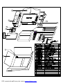
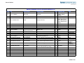
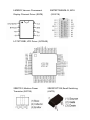
1
ENGLISH
HS 200 Home Cinema System
SERVICE MANUAL
ENGLISH
Front Panel Controls
Main Information Display
1 Power On/Off (Standby)
2 Eject
3 USB On-The-Go Input
4 Headphone Jack
5 Volume Control
6 Slot Loader
Main Information Display: This display
delivers messages and status indications to help
you operate the HS 200 Controller.
3 USB On-The-Go Input: This input may be
used to temporarily connect a USB thumb device
or portable hard disk for direct playback of
audio, image of video files or a USB hub. The
USB inputs are designed to power a single USB
device at a time. If additional hard disks are
connected through a hub it is necessary that
additional external power supplies are used to
power the hub and hard disks.
4 Headphone Jack: This jack may be used to
listen to the system's output through a pair of
headphones. Be certain that the headphones
have a standard 3.5 mm stereo phone plug.
Note that the main room speakers will
automatically be turned off when the
headphone jack is in use.
1 Power On/Off (Standby): Press the button
once to turn the HS 200 Controller on, press it
again to put the unit in the Standby mode.
Note that when the HS 200 Controller is
switched on, the Power Indicator around the
button turns blue.
2 Eject: Press this button to release a disc
from the loader.
5 Volume Control: Turn this knob clockwise
to increase the volume, counterclockwise to
decrease the volume. If the system is muted,
adjusting volume control will automatically
release the unit from the silenced condition.
6 Slot loader: Gently insert a CD or DVD into
this slot, with the printed side of the disc facing
up. Note there is no drawer. Press the Eject
Button 2 to release the disc.
FRONT PANEL CONTROLS 7
Front Panel Display
A Disc Type Indicators
B Playback-Mode Indicators
C Progressive Scan Indicator
D Parental Lock Indicator
E Time Indicators
F Video Format Indicators
G Source Indicators
H Repeat Indicators
I VCD Playback Control Indicator
J Random Indicator
K A-B Repeat Indicator
L Program Indicator
M Angle Indicator
N Title Indicators
O Chapter/Track Number Indicators
P Video Output Indicators
A Disc Type Indicators: The CD or DVD
indicator will illuminate to show the type of disc
currently being played.
E Time Indicators: These positions in the
indicator will show the running time of a DVD in
play. When a CD is playing, these indicators will
show the current track time, time remaining in
the current track, or the total remaining time on
the disc.
I VCD Playback Control Indicator: This
indicator lights when the playback control
function is turned on with VCDs.
B Playback-Mode Indicators: These
indicators light to show the current playback
mode:
Lights when a disc is playing in the normal
mode
N
H Lights when the disc is in the Fast Search
Forward mode. The on-screen banner display
indicates the selected speed (2x, 8x, 16x, 100x).
1
Lights when the disc is paused.
G Lights when the disc is in the Fast Search
Reverse mode. The on-screen banner display
indicates the selected speed (2x, 8x, 16x, 100x).
C Progressive Scan Indicator: This indicator
lights when the unit sends out a progressive
scan signal.
D Parental Lock Indicator: This indicator
lights when the parental-lock system is engaged
in order to prevent anyone from changing the
rating level without a code.
8 FRONT PANEL DISPLAY
NOTE: The Indicators NOE will also display
text messages about the DVD’s status, including
Reading when a disc is loading,
STANDBY when the unit is turned off, and
Disc Error when a disc not compatible
with the DVD is put into the play position.
F Video Format Indicators: These indicators
will represent the video format currently playing.
G Source Indicators: These indicators will
light to show which source is currently selected.
H Repeat Indicators: These indicators light
when any of the Repeat functions are in use.
J Random Indicator: This indicator lights
when the unit is in the Random Play mode.
K A-B Repeat Indicator: This indicator lights
when a specific passage for repeat playback has
been selected.
L Program Indicator: This indicator lights
when the programming functions are in use.
M Angle Indicator: This indicator blinks when
alternative viewing angles are available on the
DVD currently playing.
N Title Indicators: These two positions in the
display will show the current title number when
a DVD disc is playing.
O Chapter/Track Number Indicators: When
a DVD disc is playing, these two positions in the
display will show the current chapter. When a
CD disc is playing they will show the current
track number.
P Video Output Indicators: These indicators
will represent the active video output.
4
G
B
7
F
C I
9 E8
A
H
6
0
2
D
5
3
0 Composite Video Output
7 Subwoofer Output
E Coaxial Digital Output
1 S-Video Output
8 Coaxial Digital Input
F Subwoofer Trigger Output
2 Component Video Outputs
9 Optical Digital Input
G USB On-The-Go Input
3 Scart TV Output
A Analog Audio Outputs
H HDMI Output
4 AC Power Cord
B Front Speaker Outputs
I Remote IR Output
5 FM Antenna
C Remote IR Input
6 Audio In
D TV Audio In
0 Composite Video Output: Connect this
jack to the video input on a television or video
projector.
4 AC Power Cord: Connect this plug to an AC
outlet. If the outlet is controlled by a switch,
make certain that it is in the ON position.
1 S-Video Output: Connect this jack to the SVideo input on a television or video projector.
5 FM Antenna: Connect to the supplied FM
antenna.
2 Component Video Outputs: These outputs
carry the component video signals for connection
to display monitors with component video inputs.
For standard analog TV's or projectors with
inputs marked Y/Pr/Pb or Y/Cr/Cb, connect these
outputs to the corresponding inputs. If you have
a high-definition television or projector that is
compatible with high scan rate progressive video,
connect these jacks to the “HD Component”
inputs. Note that if you are using a progressive
scan display device, then ”Progressive” must be
selected in the Video Set-up Menu in order to
take advantage of the progressive scan circuitry.
See page 20 for more information on progressive
scan video.
6 Audio In: Connect to a line-level analog
audio source: TV, tape player, Minidisc, PC, etc.
IMPORTANT: These jacks should NOT be connected to standard composite video inputs.
3 SCART OUT (TV): If your TV has a SCART
socket, you can connect a SCART cable to your
TV and to your DVD Player for improved video
quality. The SCART cable carries both audio and
video. You can select Composite Video or RGB
video for that SCART connector’s video output
signal.
7 Subwoofer Output: Connect to the
SUB/LFE input on the subwoofer.
8 Coaxial Digital Input: Connect the coax
digital output from a DVD player, HDTV receiver,
LD player, MD player, satellite receiver or CD
player to this jack. The signal may be either a
Dolby Digital signal, DTS signal or a standard
PCM digital source. Do not connect the RF digital
output of an LD player to these jacks.
1
B Front Speaker Outputs: Connect these
outputs to the matching + or – terminals on your
left and right speakers. In conformance with the
new CEA color code specification, the White terminal is the positive, or "+" terminal that should
be connected to the red (+) terminal on Front
Left speaker with the older color coding, while
the Red terminal is the positive, or "+" terminal
that should be connected to the red (+) terminal
on Front Right speaker. Connect the black (–)
terminals on the HS to the black (–) terminals on
the speakers. See page 14 for more information
on speaker polarity.
C Remote IR Input: If the HS 200’s frontpanel IR sensor is blocked due to cabinet doors
or other obstructions, an external IR sensor may
be used. Connect the output of the sensor to
this jack.
9 Optical Digital Input: Connect the optical
digital output from a DVD player, HDTV receiver,
LD player, MD player, satellite receiver or CD
player to this jack. The signal may be either a
Dolby Digital signal, DTS signal or a standard
PCM digital source.
A Analog Audio Outputs: Connect these
jacks to the analog audio input on a TV set or
external audio system for analog audio playback
or to the RECORD/INPUT jacks of an audio
recorder for recording.
REAR PANEL CONNECTIONS 9
ENGLISH
Rear Panel Connections
Rear Panel Connections
D TV Audio Input: If your screen is
connected to the HS by an HDMI, Component,
S-Video or Composite cable, connect the
analog output of your TV to this input. If you
have your TV connected to the HS with a Scart
cable, an audio connection to the TV Input is
not necessary.
Note: You’ll find more details about all
Audio/Video connections under Setup and
Connections on the following pages.
E Coaxial Digital Output: Connect this jack
to the matching digital input connector on a
digital recorder such as a CD-R or MiniDisc
recorder.
F Subwoofer Trigger Output: Connect this
trigger output to the trigger input of the
Harman Kardon subwoofer, so that the
subwoofer will switch on and off at the same
time as the rest of the system.
10 REAR PANEL CONNECTIONS
G USB On-The-Go Input: This input may be
used to temporarily connect a USB thumb device
or portable hard disk for direct playback of
audio, image of video files, a digital photo
camera or a USB hub.
H HDMI Output: Connect this output to the
HDMI input of high-definition LCD, Plasma or
video projector for the best possible picture
quality.
I Remote IR Output: This connection
permits the IR sensor in the receiver to serve
other remote controlled devices. Connect this
jack to the “IR IN” jack on Harman Kardon or
other compatible equipment.
0 Power On/Source Selection Button
1 Power Off Button
2 Subtitle Button
3 Title Button
4 Angle Button
5 Audio Button
1
6 Enter Button
7 Eject Button
8 Set-Up/OSD Button
9 Arrows Button
0
A
A Mute Button
B Menu Button
C Pause Button
D Status Button
E Skip/Step (Previous) Button
F Skip/Step (Next) Button
G Play Button
H Search/Slow Reverse Button
I STOP Button
J Search/Slow Forward Button
G
O Random Button
P A-B Repeat Button
Q Volume up/down Button
Light Button
8
B
9
N
O
M
P
Video format Button
Learn Button
Screen Power Buttons
7
H
IR Transmitter Window
Program Indicator
E
Picture in Picture Button
Screen Format Button
4
K
Clear Button
Video output Button
Teletext Buttons
6
8
D
Numeric Keys Button
Repeat Button
Info Button
5
2
K Macro Buttons
L Pic +/Pic - Button
M Zoom Button
N Playlist Button
Q
L
I
3
F
G
J
C
REMOTE CONTROL 11
ENGLISH
Remote Control
Remote Control
0 Power On/Source Selector Buttons:
Pressing one of these buttons will perform three
actions at the same time. First, if the HS System
is not turned on, this will power up the unit.
Next, it will select the source shown on the button as the input to the HS System. Finally, it will
change the remote control so that it controls the
device selected.
1 Power Off Button: Turns off the
HS system to standby mode.
2 Subtitle Button: When a DVD is playing,
press to select a subtitle language or to turn
subtitles off.
3 Title Button: When a disc is playing, press
to make the player go back to the first section of
the disc.
4 Angle Button: Press to access various
camera angles on a DVD (If the DVD contains
multiple camera angles) or to rotate JPEG
images.
5 Audio Button: Press to access various
audio languages on a DVD (If the DVD contains
multiple audio streams).
6 Enter Button: Press this button to activate
a setting or option.
7 Eject Button: Press to release the disc
from the loader.
8 Set-up/OSD: Press to access the On Screen
Display Menu.
9 Arrow buttons (M / N /K/L) Buttons:
Use to move the cursor in the OSD.
A Mute Button: Mutes the sound.
B Menu Button: Displays the actual DVD
Disc Menu on the TV screen in play mode.
When playing discs with JPEG images, pressing
this button will access the thumbnails.
C Pause Button: Freezes a picture (with
DVD/VCD) and pauses the playback signal (CD)
when a disc is playing. Press again for normal
playback.
D Status Button: Press while a disc is playing to view banner display. Use the ARROW buttons to move through the different features in
the Banner Display. When a symbol is highlighted, press ENTER on the remote to select it.
12 REMOTE CONTROL
E Skip/Step (Previous) Button: Press to go
to beginning of current track. Press again quickly
to go to beginning of previous track. After pressing the PAUSE button, each press of this button
will move the image in reverse frame by frame.
F Skip/Step (Next) Button: Press to go to
beginning of next track. After pressing the PAUSE
button, each press of this button will move the
image forwards frame by frame.
N Playlist Button: Press this button to
change the playback order of the disc.
O Random Button: Press for RANDOM
playback in random order.
P A-B Button: Press to select section A-B and
to play repeatedly.
Q Volume Up/Down: Increase/
decrease the master volume level.
G Play Button: Begins to play disc (closes
disc tray first, if it is open).
LIGHT Button: Press to illuminate remote
controller.
H Search/Slow (Rev.) Button: Allows you
to search in reverse through a disc while it is in
play mode. Each time you press this button, the
search speed changes as indicated by a number
of arrows on the right top of your screen.
After pressing the PAUSE button, each press of
this button will change the slow down speed
indicated by a number of arrows in the right top
of the screen.
Numeric Keys Button: Select numbers by
pressing these buttons.
I Stop Button: Stops playing a disc. When a
disc is playing, if you press STOP and PLAY, the
disc will resume play, i.e. it will start from the
same point on the disc where the unit was
stopped. If you press STOP twice and the PLAY
button, the disc will start play from the beginning.
J Search/Slow (Fwd.) Button: Allows you
to search forward through a disc while it is in
play mode. Each time you press this button, the
search speed changes as indicated by a number
of arrows on the right top of your screen.
After pressing the PAUSE button, each press of
this button will change the slow down speed as
indicated by a number of arrows in the right top
of the screen.
K Macro Buttons: Press these buttons to
store or recall a “Macro”, which is a pre-programmed sequence of commands stored in the
remote. (See page 26 for more information on
storing and recalling macros.).
L Pic +/Pic - Button: Pressing these buttons
in JPEG mode will move to the previous or next
image.
M Zoom Button: When a DVD or VCD is
playing, press this button to zoom the picture so
that it is enlarged. There are 4 steps to the zoom
function, each progressively larger. Press through
each of the zoom stages to return to a normal
picture. The Zoom function is not available when
watching High Definition material.
Repeat Button: Press to go to the Repeat
menu. You can repeat a chapter, track or the
entire disc.
Clear Button: Press to remove the Banner
menu from the screen.
Video output Button: Press to toggle
between the S-Video, Component Video Outputs
and SCART RGB video output of the HS Sysrem
player. Note that the Composite and SCART
Composite Video Outputs on the player are
always active, which could help you make your
initial setup.
Video format Button: Press this button to
change the resolution of the Component Video
Output between standard definition and
progressive definition (PAL interlaced and PAL
progressive; NTSC interlaced and NTSC
progressive).
Learn Button: Press this button to begin
the process of “learning” the codes from another
product’s remote into the HS System’s remote.
(See page 26 for more information on using the
remote’s learning function.)
to
These buttons do not have a direct
function with the HS 200, but can be
programmed to control some of the functions of
your TV using the Learning function of the
remote control.
IR Transmitter Window: Point this window
towards the HS when pressing buttons on the
remote to make certain that infrared commands
are properly received.
Program Indicator: This three-color
indicator is used to guide you through the
process of learning commands from a remote
into the HS’s remote code memory. (See page
26 for more information on programming the
remote.)
Troubleshooting
If you experience any of the following difficulties
while using the system, use this troubleshooting
guide to help you remedy the problem.
Should any problem persist, consult your
authorized Harman Kardon dealer.
No power.
• Is the power cord firmly plugged into the
power outlet?
• One of the safety mechanisms may be
operating. In this event, unplug the player from
the power outlet briefly and then plug it in
again.
There is no sound or volume is very low.
• Check that the speakers and components are
connected correctly and securely.
The remote does not function.
• Remove any obstacles between the remote
control and the system.
• Make sure that you have selected the correct
source on the system.
• Move the remote control closer to the system.
• Press MUTE on the remote control, if the
words MUTE ON are blinking on the front
panel display.
• The protective circuitry has been activated
because of a short circuit. Turn off the system,
eliminate the short circuit problem and turn on
the power again.
• The audio interconnect is damaged. Replace it
with a new one.
No picture.
• Check that the system is connected correctly
and securely.
• The system is in pause mode or in slow-motion
play mode, or fast forward or fast reverse.
Press N to return to normal play mode.
• The video cable may be damaged. Replace it
with a new one.
• Check the speaker settings (see page 19).
• Make sure the system is connected to a video
input on the TV (see page 14).
The left and right channels are unbalanced
or reversed.
• Check that the speakers and components are
connected correctly and securely.
• Make sure the TV is turned on.
• Make sure the correct video input on the TV is
selected for viewing with this system.
Noise (interference) appears in the
picture.
• Clean the disc.
• If video from this system has to go through
your VCR to get to your TV, the copy-protection
applied to some DVD programs could affect
picture quality. If you still experience problems
after checking your connections, please try
connecting your DVD system directly to your
TV’s S-Video input, if your TV is equipped with
this input (see page 14).
The aspect ratio of the screen is wrong
(picture vertically expanded) when you
play a wide picture even though you set
“TV DISPLAY” in the SETUP menu to
"16:9".
• If you connect the system with the SCART
cable, connect directly to the TV. Otherwise the
autoswitch function of the aspect ratio for the
TV may not work.
• If the TV is not connected with a SCART cable
to the HS, or if the autoswitch function does
not work you should turn the TV to "16:9" (if
possible with your TV).
• Depending on the TV, you may not be able to
change the aspect ratio. In that case (TV not
adjustable to 16:9) do not select "16:9" in the
TV Display. Then, no change of the aspect ratio
is needed.
28 TROUBLESHOOTING
Severe hum or noise is heard.
• Check that the speakers and components are
connected securely.
• Check that the connecting cords are away from
a transformer or motor and at least 3 meters
away from fluorescent light.
• Move your TV away from the audio
components.
• The plugs and jacks are dirty. Wipe them with a
cloth slightly moistened with alcohol.
• Clean the disc.
The volume goes down automatically
and can not be increased.
• The internal temperature is too high. Wait
approximately one minute for the amplifier to
reach normal working temperature.
Radio stations cannot be tuned in.
• Check that the antenna is connected correctly.
Adjust the antenna and connect an external
antenna if necessary.
• The signal strength of the stations is too weak
for automatic tuning. Use manual tuning.
• No stations have been preset.
• The tuner mode is not selected, select the
Radio mode.
• Point the remote control at the remote sensor
on the front panel.
• Replace all the batteries in the remote control
with new ones if they are weak.
• Check that the batteries are loaded correctly.
The disc does not play.
• There is no disc inside. (“NO DISC” appears on
the front panel display and the TV screen.)
Insert a disc.
• Insert the disc correctly with the playback side
facing down on the disc tray.
• Clean the disc.
• The system cannot play CD-ROM's, etc.
(see page 3).
• DVD with wrong region code
(see page 13).
The system starts playing the DVD
automatically.
• The DVD features the auto playback function.
Playback stops automatically.
• Some discs include an auto pause signal. When
playing such a disc, the system stops playback
at the signal.
Track Skip or direct select with numeric
buttons, Search, Slow-motion play, repeat
play or Program play, etc., cannot be done.
• Depending on the DVD or VCD, some of the
above operations may not be available
(Playback control).
Messages do not appear on the TV screen
in the language you want.
• Select the language for Display and Preferred
Subtitle in the SETUP menu (see page 18).
For all messages from the DVD (DVD menu,
subtitles) in the proper language the disc must
have the language you selected, if not, another
language will be selected.
The audio language cannot be changed
when you play a DVD.
• Multilingual sound is not recorded on the DVD.
• Changing the language for the sound by the
Audio button on the remote or the Audio line
in the Player Menu is prohibited on the DVD.
In that case the audio language must be
selected by the main menu on the DVD.
ENGLISH
Troubleshooting
The subtitles cannot be turned off when
you play a DVD.
• Depending on the DVD, you may not be able to
turn the subtitles off.
The angles cannot be changed when you
play a DVD.
• Multi-angles are not recorded on most DVDs.
• Change the angles when the angle mark
appears on the TV screen.
• Changing the angles is prohibited on some
DVDs.
The system does not operate properly.
• Static electricity, etc., may affect the system’s
operation.
Disconnect the AC power cord, then connect it
again.
Please also refer to the Troubleshooting
guide contained in your loudspeaker
Owners Manual.
The subtitle language cannot be changed
when you play a DVD.
• Multilingual subtitles are not recorded on the
DVD.
• Changing the language for the subtitles by the
Subtitle button on the remote or the Subtitle
line in the Player Menu is prohibited on the
DVD. In that case the subtitle language must
be selected by the main menu on the DVD.
TROUBLESHOOTING 29
Glossary
Bit rate
Value indicating the amount of video data compressed in a DVD per second. The unit is Mbps
(megabit per second). 1 Mbps indicates that the
data per second is 1,000,000 bits. The higher the
bit rate, the larger the amount of data. However,
this does not always mean higher quality
pictures.
Chapter
Sections of a picture or a music piece on a DVD
that are smaller than titles. Many titles are composed of several chapters, but many others are
not. Each chapter is assigned a chapter number
enabling you to locate the chapter you want.
Dolby Digital (“5.1”, “AC-3”)
This sound format for movie theaters is more
advanced than Dolby Pro Logic Surround. In this
format, the rear speakers output stereo sound
with an expanded frequency range and a subwoofer channel for deep bass is independently
provided. This format is also called “5.1” because
the subwoofer channel is counted as 0.1 channel
(since it functions only when a deep bass effect is
needed). All six channels in this format are
recorded separately for superior channel
separation. Furthermore, since all the signals are
processed digitally, less signal degradation
occurs. The name “AC-3” comes from the fact
that it is the third audio coding method to be
developed by the Dolby Laboratories Licensing
Corporation.
Manufactured under license from Dolby
Laboratories. "Dolby", "AC-3", "Pro Logic" and
the Double-D symbol are trademarks of Dolby
Laboratories. Confidential Unpublished Works.
© 1992.1997 Dolby Laboratories, Inc. All rights
reserved.
Dolby Pro Logic II Surround
This is a method of decoding stereo or surround
recordings that produces five channels from twochannel sound. Compared with the former Dolby
Surround system, Dolby Pro Logic II Surround
reproduces left-to-right panning more naturally
and localizes sounds more precisely. To take full
advantage of Dolby Pro Logic II Surround, you
should have a pair of rear speakers and a center
speaker. The rear speakers output stereo sound.
DTS
Digital audio compression technology developed
by Digital Theater Systems, Inc. This technology
conforms to 5.1-channel surround. The rear
channels are stereo and there is a discrete
subwoofer channel in this format. DTS provides
5.1 discrete channels of high quality digital
audio. Good channel separation is realized,
because all channels are recorded discretely and
processed digitally.
30 GLOSSARY
Manufactured under license from Digital Theater
Systems, Inc. US Pat. No. 5,451,942 and other
worldwide patents issued and pending. "DTS"
and "DTS Digital Surround" are trademarks of
Digital Theater Systems, Inc.
© 1996 Digital Theater Systems, Inc.
All rights reserved.
Title
The longest sections of a picture or a music piece
on a DVD; a movie, etc., for a picture piece on
video software; or an album, etc., for a music
piece on an audio software. Each title is assigned
a title number enabling you to locate the title
you want.
MPEG AUDIO
International standard coding system to compress audio digital signals authorized by ISO/IEC.
MPEG 1 conforms to up to 2-channel stereo,
used on some DVD’s as alternate (other language) track.
Track
Sections of a music piece on a CD. Each track is
assigned a track number enabling you to locate
the track you want.
DVD
A disc that contains up to 8 hours of moving
pictures even though its diameter is the same as
a CD. The data capacity of a single-layer and
single-sided DVD, at 4.7 GB (Giga Byte), is
7 times that of a CD. Furthermore, the data
capacity of a dual-layer and single-sided DVD is
8.5 GB, a single-layer and double-sided
DVD 9.4 GB, and a dual-layer and double-sided
DVD 17 GB. The picture data uses the MPEG 2
format, one of the worldwide standards of digital
compression technology. The picture data is
compressed to about 1/40 of its original size.
The DVD also uses the variable rate coding
technology that changes the data to be allocated
according to the status of the picture. The audio
data is recorded in Dolby Digital, DTS and/or
PCM, allowing you to enjoy more natural audio
presence. Furthermore, various advanced
functions such as multi-angle, multilingual, and
subtitles may be provided with the DVD.
Multi-angle function
Various angles or viewpoints of the video camera
for a scene are recorded on some DVDs.
Multilingual function
Several languages for the sound or subtitles in a
picture are recorded on some DVDs.
Parental Control
A function of some (particulary US) DVD’s to limit
playback of the disc by the age of the users.
The limitation varies from disc to disc. When it is
activated, playback is completely prohibited,
violent scenes are skipped or replaced with other
scenes and so on.
PCM
Pulse code modulation, an uncompressed data
formation.
NTSC
National TV Systems Committee: a video
standard used in USA.
PAL
Phase Alternation Line: a video standard used in
many European countries.
ENGLISH
HS 200 Controller Specifications
DVD player
Pickup:
Semiconductor laser, wavelength 650nm
Signal system:
NTSC / PAL
Video signal horizontal resolution:
More than 480 lines (DVD)
Video signal-to-noise ratio:
More than 60 dB (DVD)
Audio frequency response:
(Stereo)
DVD (PCM): 20 Hz ~ 22 kHz (+/- 1.0 dB)
CD (PCM): 20 Hz ~ 20 kHz (+/- 1.0 dB)
Audio signal-to-noise ratio:
More than 80 dB (PCM)
Total harmonic distortion:
Less than 0.01% (PCM)
Dynamic range:
DVD (PCM): More than 85 dB (EIAJ, 2 kHz)
CD:
More than 85 dB (EIAJ)
System:
PLL quartz-locked digital synthesizer system
Tuning range:
87.50 ~ 108.00 MHz
Antenna terminals:
75 Ohms, unbalanced
Intermediate frequency:
10.7 MHz
FM Tuner
Video Outputs HDMI
Component Video Output:
Y: 1 Vp-p/75 Ohms, sync negative polarity
Cr: 0.7 Vp-p/75 Ohms
Cb: 0.7 Vp-p/75 Ohms
CVBS Video:
1 Vp-p 75 Ohms
S-video:
Y: 1 Vp-p 75 Ohms
C: PAL 0.3 Vp-p 75 Ohms / NTSC 0.286 Vp-p 75 Ohms
Audio line Outputs
Audio L/R:
2 Vrms, 1 kilohms
Power requirements:
AC 230 V, 50 Hz
Max power consumption:
300 W
Idle power consumption:
Less than 2 W
Dimensions (WxHxD):
350mm x 84mm x 250mm
Weight:
3.8 kg
General
* Designs and specifications are subject to change without notice.
Depth measurement includes knobs, buttons and terminal connections. Height measurement includes feet and chassis.
All features and specifications are subject to change without notice.
Harman Kardon is a registered trademark of Harman International Industries, Incorporated.
Dolby, Pro Logic and the double-D symbol are trademarks of Dolby Laboratories, registered in the United States and/or other countries. All rights reserved.
DTS is a trademark of Digital Theater Systems, Inc.
Windows Media® Audio (WMA) is a proprietary file format developed by Microsoft.
DivX is a registered trademark of DivX, Inc.
HDMI, the HDMI logo and High-Definition Multimedia Interface are trademarks or registered trademarks of HDMI Licensing LLC.
HS 200 CONTROLLER SPECIFICATIONS 31
PDF created with pdfFactory trial version www.pdffactory.com
19
16
17
17
15
14
13
18
6
12
11
9
5
4
3
8
7
10
2
1
2
PDF created with pdfFactory trial version www.pdffactory.com
harman/kardon
HS200 Component List
Item P/N
Description
Specification
1
2
3
4
5
6
0100WJTJHS200E001
0100WJTJHS200E002
0100WJTJHS200E003
0100WJTJHS200E004
0100WJTJHS200E005
0100WJTJHS200E006
metals part
metals part
metals part
metals part
metals part
metals part
HS200-chassis
HS200-top cover
HS200-rear panel
HS200-rear panel
HS200-PCB plastic frame(Left)
HS200-PCB plastic frame(Right)
Qty Location.No.
1
1
1
1
1
1
HS200-PT01
HS200-PT02
HS200-PT03
HS200-PT03
HS200-PT04
HS200-PT05
7
0100WJTJHS200E007
metals part
HS200-Connected Piece for Speaker Jack
4
HS200-PT06
8
9
01.00.WJ.TJ.E889
01.00.WJ.TJ.E890
Heatsink
Heatsink
50*62*65MM
39*54.5*61mm
1
1
HS200-PT07
HS200-PT08
10
01.00.WJ.TJ.E891
Heatsink
122*45*51mm
1
HS200-PT09
11
01.00.WJ.TJ.E892
Heatsink
35*30*49mm
1
HS200-PT10
12
01.00.WJ.TJ.E893
Heatsink
16*12*51MM (The Hole's depth is 18MM
4
13
01.00.WJ.TJ.E268
Heatsink
28*28*10mm
1
14
01.13.L.H.E034
Magnetism annulus
F5BRFS11.7*6*19.75-3-P.W
2
15
16
17
18
19
20
21
22
23
0100SJHS200E001
0100SJHS200E002
0100SJHS200E003
0100SJHS100E006
0100SJHS200E004
0100SJHS200E005
0100SJHS200E006
0100SJHS200E007
0100SJHS200E008
plastic part
plastic part
plastic part
plastic part
plastic part
plastic part
plastic part
plastic part
plastic part
HS200-front panel
HS200-2 in 1 Button
HS200-Open button collar
HS100 Volume Button Collar
HS200-Button Cover Board
HS200-Power Indicator lampshade
HS200-pedestal underlay
HS200-Power Jack Jacket
HS200-plastic scaleboard
1
1
1
1
1
1
2
1
1
For
S503/S504/S505/S506
on SMPS Board
For U4 of Main Board
For Amplifier Output
Cord
HS200-RE01
HS200-RE02
HS200-RE03
HS100-RE06
HS200-RE04
HS200-RE05
HS200-RE06
HS200-RE07
HS200-RE08
Note
Appointed Color
EU Vision
US Vision
For AV Board
For AV Board
For SMPS
Board
For SMPS
Board
ABS, Black
transparent
transparent
HS200 /230
harman/kardon
HS200 Component List
Item P/N
Description
Specification
Qty Location.No.
24
0100SJHS200E009
plastic part
HS200-Large Lens
1
HS200-RE10
25
26
27
28
29
30
0100SJHS100E010
0100SJHS100E008
0100SJ1000AE016
01.00.SJ.QT.E019
01.40.CON.DCZ.E178
01.00.SB.E036
HS100 Volume Button
HS100 volume button lampshade
1000A-IR receiver support 5.5mm
124.5*33.5*0.5mm
WS-044-0
100mm "Harman/Kardon" Thin Logo
1
1
1
1
1
1
HS100-RE10
HS100-RE08
31
01.00.DP.JY.E135
plastic part
plastic part
plastic part
VFD filter
AC power Jack
Metal logo
Dustproof for Disc tray door of
Loder
LTD-1510
1
32
01.00.DP.XJ.E192
Silica gel gasket
33
01.00.DP.HM.E359
sponge
34
01.00.FZ.QT.153
Astigmatism PVC
Φ45.5*Φ9.5mm
1
35
36
01.00.FZ.QT.E253
01.00.DP.HM.E364
Mask PVC
sponge
φ38.5 (Underside Glued)
10*10*7MM (with double sides glued)
1
1
37
01.00.DP.HM.E160
sponge
20*10*4.5mm (with Single side glued)
1
38
01.00.DP.HM.E363
High Soft sponge
124*12*2MM (with Single side glued)
1
39
01.00.DD.PM.E183
electric sponge
12*10*18mm
1
40
01.00.DD.PM.E271
electric sponge
20*20*10MM
1
41
01.00.FZ.QT.E122
Plastic fastener
12CM
3
42
01.00.DP.QT.E113
Sil-pad
sil-pad 400-3022
1
50.6*4.2*1.5mm (with #500 glue be single
sides glued )
20*10*7MM (with #9448 glue be double
sides glued )
Note
3mm Black
Lens (Include
"HS200" and
47mm
“harman/kardon
” Logo)
Black
4
For pedestal underlay
HS100-H01
2
For VFD(2)
Between volume button
and Front Panel Board
Inside the volume button Black PVC
For IR receiver
Between AV Board and
Black
Heatsink
paste in front of Disc
tray door in the front
Black
panel
pasted under U403 of
AV Board
Between front panel
PCB and plastic part
For Q509 on SMPS
Board
HS200 /230
harman/kardon
HS200 Component List
Item P/N
Description
Specification
Qty Location.No.
43
01.00.DP.JY.E112
44
01.00.DP.JY.E247
Diathermanous Selenium
Rubber
Insulated PVC
45
01.00.DP.JY.E249
Insulated PVC
HS200-H02
1
46
01.00.DP.JY.E541
Insulated PVC
22.5*10*0.3mm (with Single side glued)
2
47
01.00.DP.HM.E369
sponge
15*15*24mm (with Single side glued)
1
48
01.00.DP.HM.E370
sponge
15*15*7mm (with Single side glued)
1
49
01.00.DP.HM.E115
sponge
10*10*1.5mm
1
50
01.00.DP.XJ.E560
Diathermanous Silica gel
gasket
20*15*4MM
2
51
01.00.WJ.JG.E265
Screw
3*8PWBTTC
2
52
01.00.WJ.JG.E328
Screw
3*6KBTTO
5
53
01.00.WJ.JG.E543
Screw
3*6PWBTTNI
9
54
01.00.WJ.JG.E235
Screw
3*8PWBTTNI
3
55
01.00.WJ.JG.E655
Screw
1.7*4CAHNI D=3.2 Free-Lead
1
16*11*1mm
3
For AV Board
HS200-H01
1
For SMPS Board
Be buckled above
volume button board
For hamulus of front
panel
For frequency
modulation module and
AV Board
For frequency
modulation module and
Main Board
For hamulus of front
panel
Between AV Board and
chassis under U403
For AV Board and
Heatsink (2)
For front Panel and
Left/Right sides of
chassis (4), Between
two Heatsinks on SMPS
Board(1)
For pedestal underlay
and chissis (9)
For front panel and
pedestal underlay and
chissis(3)
For Button cover Board
and button Board
Note
HS200 /230
harman/kardon
HS200 Component List
Item P/N
Description
Specification
Qty Location.No.
56
01.00.WJ.JG.E166
Screw
3*8PAHC
10
57
01.00.WJ.JG.E085
Screw
3*6KBTTNI
2
58
01.00.WJ.JG.E091
Screw
3*6PWBTTC W=7
8
59
01.00.WJ.JG.E451
Screw
3*6PWMHC W=7
11
60
01.00.WJ.JG.E252
Screw
3*4RBTTNI
6
61
01.00.WJ.JG.E417
Screw
3*8PBTTC
9
62
01.00.WJ.JG.E321
Screw
3*8PAHO
9
63
01.00.WJ.JG.E675
Screw
3*10PAHO
3
64
01.00.WJ.JG.E403
Screw
3*6PWBTTO
5
65
01.00.WJ.JG.E865
Screw
3*12PMHO
2
Note
For front panel and front
panel board(9) For
plastic scaleboard and
Speaker Connected
Board (1)
For front panel and
volume button board
For Loader and
chassis(4), For PCB
Brackets and chassis
(4)
For SMPS Board and
chassis (5), For AV
Board and chassis (3),
For Main Board and
PCB brackets (3)
For rear panel and the
bottom side of chassis
(2), For top cover and
bottom side of chassis
(4)
For ICs and Heatsinks
on SMPS Board (7), For
Two sorts of Heatsinks
on AV Board (2)
For output jacks (7), For
frequency modulation
module (2)
For plastic scaleboard
and rear panel (3)
For top cover and
chassis, top cover and
rear panel (5)
For AC power socket (2)
HS200 /230
harman/kardon
HS200 Component List
Item P/N
Description
Specification
66
01.00.WJ.JG.E502
Screw
3*10 PMHO
Qty Location.No.
2
67
01.00.WJ.JG.E087
Screw
3*6PBTTC
2
68
69
01.00.WJ.JG.E119
01.00.WJ.JG.E119
Nut
Nut
M3
M3
2
2
70
01.00.FZ.TG.E025
Screw Jacket
Ф3*4mm
7
71
01.00.WJ.JG.E426
Flat Pad
M3*0.5 W=8
4
72
01.00.SJ.QT.E104
plastic rivet
MBL3-2.5
2
73
01.00.WJ.JG.E424
Spring Pad
M3
4
74
75
76
77
78
79
01.00.WJ.QT.E049
01.00.WJ.QT.E048
01.00.WJ.QT.E050
01.00.BZ.F.P.E613
01.00.BZ.F.P.E614
01.00.BZ.X.B.E511
Speaker Connective Stick
Speaker Connective Stick
Speaker Connective Stick
Polyfoam
Polyfoam
Accessories box
HS200 Connective Stick-Red
HS200 Connective Stick-Black
HS200 Connective Stick-White
HS200-Left
HS200-Right
HS200 340*170*45mm
1
2
1
1
1
1
80
01.00.BZ.X.W.E712
Carton box
HS200 EU Vision
1
81
01.00.BZ.X.W.E896
Carton box
HS200 US Vision
1
82
01.00.BZ.X.W.E713
Big colored carton box
HS200 EU Vision
1
83
01.00.BZ.X.W.E899
Big colored carton box
HS200 US Vision
1
Note
For SCART Jack (2)
EU Vision
For U503/D502 on
SMPS Board
For SCART Jack (2)
EU Vision
For power jack2)
For uncovered Screw
drilled through the
chassis
For Heatsink and AV
Board (2), For Two sorts
of Heatsinks on AV
Board (2)
For Insulated gasket
and volume button
Board
For Heatsink and AV
Board (2), For Two sorts
of Heatsinks on AV
Board (2)
For accessories
For unit and accessory
box packing
For unit and accessory
box packing
According to client, for
external box and
loudspeaker
According to client, for
external box and
loudspeaker
White
EU Vision
US Vision
EU Vision
US Vision
HS200 /230
harman/kardon
HS200 Component List
Item P/N
Description
Specification
Qty Location.No.
84
01.00.YS.FY3.E1176
85
86
87
88
89
90
91
92
93
01.00.YS.FY3.E1177
01.00.YS.FY3.E1178
01.00.YS.SM1.E786
01.00.YS.SM1.E947
01.00.YS.TZ.T.E068
01.00.YS.TZ.T.E057
01.00.RC.EHS200
01.14.DX.B.E0007G
01.00.BZ.D.S.E109
Safety and Warning instruction
manual
Safety and Warning card
Guarantee card
Owner manual
Owner manual
Laser label
Laser label
Remote control
Alkalescent battery
Plastic bag for unit
94
01.00.BZ.D.Z.E020
Plastic bag
25*35cm
1
95
01.00.BZ.D.Z.E034
Plastic bag
9*27.5CM
1
96
97
98
01.00.BZ.D.Z.E008
01.00.BZ.D.H.E002
0147CNTLJX5E163
Plastic bag
ROHS bag
HDMI Cord
1
1
1
99
01.47.CNT.ACX.E052
Power Cord
100
01.47.CNT.ACX.E053
Power Cord
101
0147CNTLJX5E058
Connect cable
102
01.47.CNT.CTX.E016
Antenna
103
104
105
01.47.CNT.CTX.E038
01.47.CNT.CTX.E042
0115JXEDL05FHH40P
Antenna
Antenna
Loader
6*9cm
11*28cm
CJS8T001Z
WS-002E+WS-019 HO5VV-F 0.75×2C BK
2M
WS-002E+WS-004A SJT18AWG×2C BK
2M
scart 1.5m
FM-TV-22 (Lead content less than
300PPM)
FM-TV-75-A
AM-300-AWM
DL-05FH-H40P
106
01.49.E11
FM frequency modulation
module
TFCF1E806A
1
107
01.49.E07
FM/AM frequency modulation
TFCF1E804A
module
1
Note
HS200 EU Vision
1
EU Vision
HS200 US Vision
HS200 US Vision
HS200 EU Vision
HS200 US Vision
Laser precausion mark
Laser precausion guide
HS200-RC
GP7#
47*50cm
1
1
1
1
1
1
1
3
1
US Vision
US Vision
EU Vision
US Vision
For unit Packing
For Owner manual
Packing
For Remote Control
Packing
For battery Packing
For power cord packing
1
EU Vision
1
US Vision
1
EU Vision
1
EU Vision
1
1
1
US Vision
US Vision
IEC Head for FM
Connector (NON-Screw EU Vision
Thread)
F Head for FM
Connector (Screw
US Vision
Thread)
HS200 /230
harman/kardon
HS200 Component List
Item P/N
Description
Specification
Qty Location.No.
108
0147CNTLJX7E603
Connect cable
VH-3Y Connector-2Y-120mm(Be same
side)
1
109
0147CNTLJX7E615
Connect cable
VH-3Y Connector-2Y-2Y-100mm(Be same
side)
1
110
0147CNTLJX7E649
Connect cable
VH-4Y Connector-4Y-60mm(Be same
side with color is White, Black, Red and
Black)
1
111
01.48.BPX.1.E147
Flat cable
1.0*14P*100mmA
1
112
01.48.BPX.1.E148
Flat cable
1.0*8P*100mmA
1
113
01.48.BPX.1.E149
Flat cable
1.25*12P*80mmA(T=0.1mm)
1
114
01.48.BPX.1.E150
Flat cable
1.0*16P*80mmA
1
115
01.48.BPX.1.E151
Flat cable
1.0*24P*80mmA
1
116
01.48.BPX.1.E152
Flat cable
1.0*5P*80mmA
1
117
01.48.BPX.1.E153
Flat cable
1.25*14P*70mmA(T=0.1mm)
1
118
01.48.BPX.1.E154
Flat cable
1.0*6P*40mmA
1
Note
CN501 on SMPS Board
to Power Jack with
solder one end
CN506 on SMPS Board
to CN403(L) on AV(L)
Board
CN405 on AV Board to
JP1.JP2 JP3.JP4 on
Speaker Connected
Board with solder one
end
CN3(A) on Main Board
to CN601(A) on Front
Panel Board
CN4(B) on Main Board
to CN603(B) on Front
Panel Board
CN5(C) on Main Board
to CN504(C) on SMPS
Board
CN9(D) on Main Board
to CN301(D) on AV
Board
CN8(E) on Main Board
to CN302(E) on AV
Board
CN6(G) on Main Board
to CN304(G) on AV
Board
CN503(H) on SMPS
Board to CN602(H) on
Front Panel Board
CN604(J)on Front Panel
Board to CN605(J) on
Volume Button Board
HS200 /230
harman/kardon
HS200 Component List
Item P/N
Description
Specification
Qty Location.No.
Note
CN505(K) on SMPS
Board to CN402(K) on
AV Board
For Loader and CN1 on
Main Board
For Loader and CN2 on
Main Board
For frequency
modulation module and
CN10 on Main Board
119
01.48.BPX.1.E155
Flat cable
1.25*9P*60mmA(T=0.1mm)
1
120
01.48.BPX.1.E156
Flat cable
1.0*12P*220mmA
1
121
01.48.BPX.1.E028
Flat cable
0.5*24P*200mmA
1
122
01.48.BPX.1.E157
Flat cable
1.25*11P*50mmA
1
123
0211HAV06M3627C02
HAV06M-3627C02 (EU Vision+Hitachi
Loader)
1
4-layers
124
0214HAV06I3522C02
HAV06I-3522C02 (EU Vision)
1
2-layers
125
0219HAV06P3521C01
HAV06P-3521C01
1
2-layers
126
0215HAV06K3517C01
HAV06K-3517C01
1
2-layers
127
0215HAV06K3518C01
HAV06K-3518C01
1
2-layers
128
0137PCB2E3520C1
Main Board (semimanufactured goods)
AV Board (semi-manufactured
goods)
SMPS Board (semimanufactured goods)
Front Panel Board (semimanufactured goods)
Front Panel Board (semimanufactured goods)
Speaker Connected Board
3520C-V1.0
1
2-layers
HS200 Component List for Main Board(3627C)
Item P/N
Description
Specification
Qty Location.No.
1
01.57.R.2.E000J
Resistor, chip
0603-0Ω ±5%
8
2
3
01.57.R.2.E100J
01.57.R.2.E200J
Resistor, chip
Resistor, chip
0603-10Ω±5%
0603-20Ω±5%
3
4
4
01.57.R.2.E220J
Resistor, chip
0603-22Ω±5%
10
Note
R4 R9 R45 R49 R50
R58 R181 FB53
R132 R156 R158
R42 R43 R61 R62
R29 R30 (R31) R32
(R33) R34 (R35) R36
(R37) R38
HS200 /230
harman/kardon
HS200 Component List for Main Board(3627C)
Item P/N
Description
Specification
Qty Location.No.
5
01.57.R.2.E330J
Resistor, chip
0603-33Ω±5%
14
6
01.57.R.2.E680F
Resistor, chip
0603-68Ω ±1%
1
7
01.57.R.2.E750F
Resistor, chip
0603-75Ω±1%
17
8
01.57.R.2.E101J
Resistor, chip
0603-100Ω±5%
8
9
10
01.57.R.2.E151J
01.57.R.2.E201J
Resistor, chip
Resistor, chip
0603-150Ω±5%
0603-200Ω±5%
1
1
11
01.57.R.2.E221J
Resistor, chip
0603-220Ω±5%
5
12
13
14
15
16
17
18
19
01.57.R.2.E271J
01.57.R.2.E391J
01.57.R.2.E4751F
01.57.R.2.E821J
01.57.R.2.E102J
01.57.R.2.E122J
01.57.R.2.E152J
01.57.R.2.E182J
Resistor, chip
Resistor, chip
Resistor, chip
Resistor, chip
Resistor, chip
Resistor, chip
Resistor, chip
Resistor, chip
0603-270Ω±5%
0603-390Ω±5%
0603-475Ω 1%
0603-820Ω±5%
0603-1KΩ±5%
0603-1.2KΩ±5%
0603-1.5KΩ±5%
0603-1.8KΩ±5%
1
1
1
1
2
2
2
2
20
01.57.R.2.E202J
Resistor, chip
0603-2KΩ±5%
9
21
22
01.57.R.2.E302J
01.57.R.2.E392J
Resistor, chip
Resistor, chip
0603-3KΩ±5%
0603-3.9KΩ±5%
3
3
23
01.57.R.2.E472J
Resistor, chip
0603-4.7KΩ±5%
19
Note
R2 R47 R124 R125
R126 R127 R142 R145
R146 R147 R149 R151
R153 R155
R99
R97 R98 R100 R101
R102 R103 R104 R105
R106 R107 R108 R109
R110 R111 R114 R116
R117
R6 (R41) (R71) (R120)
(R121) R130 (R133)
R139
R150
R8
R19 R136 R137 R138
R140
R173
R167
R141
R183
R26 R77
R80 R83
R79 R86
R160 R161
R13 R14 R15 R16
R18 R87 R92 R112
R115
R65 (R188) (R189)
R44 R46 R52
R5 R27 R55 R57 R63
R96 R118 R131 R135
R162 R163 R168 R170
R178 R185 R186 R190
R191 R192
HS200 /230
harman/kardon
HS200 Component List for Main Board(3627C)
Item P/N
Description
Specification
24
25
01.57.R.2.E512J
01.57.R.2.E682J
Resistor, chip
Resistor, chip
0603-5.1KΩ±5%
0603-6.8KΩ±5%
Qty Location.No.
1
1
26
01.57.R.2.E103J
Resistor, chip
0603-10KΩ±5%
16
27
28
29
30
31
32
01.57.R.2.E123F
01.57.R.2.E153J
01.57.R.2.E223J
01.57.R.2.E273J
01.57.R.2.E333J
01.57.R.2.E393J
Resistor, chip
Resistor, chip
Resistor, chip
Resistor, chip
Resistor, chip
Resistor, chip
0603-12KΩ±1%
0603-15KΩ±5%
0603-22KΩ±5%
0603-27KΩ±5%
0603-33KΩ±5%
0603-39KΩ±5%
2
2
2
1
1
1
33
01.57.R.2.E473J
Resistor, chip
0603-47KΩ±5%
5
34
35
36
01.57.R.2.E105J
01.57.R.3.E2R0F
01.57.R.4.E020J
0603-1MΩ±5%
0805-2Ω±1%
1206-2Ω±5%
1
2
1
37
01.57.R.8.EP1004
10Ω*4 ±5%
1
RN4
38
01.57.R.8.EP3304
33Ω*4 ±5%
6
RN6 RN7 RN8 RN9
RN10 RN11
39
01.57.R.8.EP4724
4.7KΩ*4 ±5%
1
RN3
40
01.57.R.8.EP1034
10KΩ*4 ±5%
1
RN1
41
01.57.R.Y.E270
AVR-M1608C270MTABB,SMD
2
ESD1 ESD2
42
01.57.R.R.E050
JK-MSMD050 SMD
1
PTC1
43
0154CS2E3P3N50V
0603-3.3P NPO±0.25%/50V
1
C192
44
0154CS2E6P8N50V
0603-6.8P NPO±0.25PF/50V
4
(C64) (C65) (C146)
(C147)
45
0154CS2E200N50V
Resistor, chip
Resistor, chip
Resistor, chip
Resistor, thick film chip
network
Resistor, thick film chip
network
Resistor, thick film chip
network
Resistor, thick film chip
network
Voltage Dependent Resistor,
TDK
Thermmal Dependent
Resistor, JinKe
Capacitor, multilayer ceramic,
chip
Capacitor, multilayer ceramic,
chip
Capacitor, multilayer ceramic,
chip
R89
R91
R24 R28 R56 R75 R76
R78 R82 R122 R123
R128 R129 R143 R144
R171 R172 R182
R48 (R72)
R17 R113
R84 R85
R90
R53
R51
R22 R54 R93 R95
R165
R73
R59 R60
R3
0603-20P NPO±5%/50V
4
C139 C140 C141 C142
Note
HS200 /230
harman/kardon
HS200 Component List for Main Board(3627C)
Item P/N
46
0154CS2E330N50V
47
0154CS2E101N50V
48
0154CS2E181N50V
49
0154CS2E221N50V
50
0154CS2E271N50V
51
0154CS2E391N50V
52
0154CS2E471X50V
53
0154CS2E561N50V
54
0154CS2E681X50V
55
0154CS2E102X50V
56
0154CS2E152X50V
57
0154CS2E272X50V
58
0154CS2E332X50V
59
0154CS2E472X50V
60
0154CS2E103Y50V
61
0154CS2E153Y50V
62
0154CS2E183X50V
Description
Capacitor, multilayer ceramic,
chip
Capacitor, multilayer ceramic,
chip
Capacitor, multilayer ceramic,
chip
Capacitor, multilayer ceramic,
chip
Capacitor, multilayer ceramic,
chip
Capacitor, multilayer ceramic,
chip
Capacitor, multilayer ceramic,
chip
Capacitor, multilayer ceramic,
chip
Capacitor, multilayer ceramic,
chip
Capacitor, multilayer ceramic,
chip
Capacitor, multilayer ceramic,
chip
Capacitor, multilayer ceramic,
chip
Capacitor, multilayer ceramic,
chip
Capacitor, multilayer ceramic,
chip
Capacitor, multilayer ceramic,
chip
Capacitor, multilayer ceramic,
chip
Capacitor, multilayer ceramic,
chip
Specification
Qty Location.No.
0603-33P NPO±5%/50V
2
(C161) (C164)
0603-100P NPO±5%/50V
2
C97 C112
0603-180P NPO±5%/50V
2
C103 C116
0603-220P NPO±5%/50V
3
C84 C87 C115
0603-270P NPO±5%/50V
1
C162
0603-390P NPO±5%/50V
1
C129
0603-470P X7R±10%/50V
3
C82 C86 C90
0603-560P NPO±5%/50V
1
C163
0603-680P X7R±10%/50V
4
C105 C106 C108 C111
0603-102 X7R±10%/50V
6
C91 C94 C96 C99 C118
C119
0603-152 X7R±10%/50V
1
(C19)
0603-272 X7R±10%/50V
1
(C20)
0603-332 X7R±10%/50V
3
C113 C114 C120
0603-472 X7R±10%/50V
1
C88
0603-103 Y5V-20+80%/50V
1
C8
0603-153 Y5V-20+80%/50V
1
C101
0603-183 X7R±10%/50V
2
C168 (C169)
Note
HS200 /230
harman/kardon
HS200 Component List for Main Board(3627C)
Item P/N
63
0154CS2E223X50V
64
0154CS2E683X50V
65
0154CS2E104Y50V
Description
Specification
Capacitor, multilayer ceramic,
0603-223 X7R±10%/50V
chip
Capacitor, multilayer ceramic,
0603-683 X7R±10%/50V
chip
Capacitor, multilayer ceramic,
0603-104 Y5V-20+80%/50V
chip
Qty Location.No.
4
C16 C117 C127 C136
2
C121 (C107)
Note
C3 C4 C6 C7 C9 C10
(C11) C12 C13 (C14)
(C15) (C17) C18 (C21)
(C22) C23 (C24) C25
(C26) (C27) (C28) (C29)
(C30) C31 C32 (C33)
(C34) (C35) (C36) (C37)
(C38) (C39) C40 C41
C42 (C43) (C44) (C45)
136
(C46) (C47) (C48) (C49)
(C50) (C51) (C52) (C53)
(C54) (C55) (C56) (C57)
(C58) (C59) (C60) (C61)
C62 (C63) C66 (C67)
(C68) (C69) (C70) (C71)
(C72) (C73) (C74) (C75)
(C76) (C77) C78
HS200 /230
harman/kardon
HS200 Component List for Main Board(3627C)
Item P/N
Description
Specification
65
0154CS2E104Y50V
Capacitor, multilayer ceramic,
0603-104 Y5V-20+80%/50V
chip
65
0154CS2E104Y50V
Capacitor, multilayer ceramic,
0603-104 Y5V-20+80%/50V
chip
66
0154CS2E105Y16V
Capacitor, multilayer ceramic,
0603-105 Y5V-20+80%/16V
chip
67
68
69
70
71
0134CLDE2U216VC
0134CLDE10U10VC
0134CLDE10U16VC
0134CLDE22U16VC
0134CLDE33U10VC
Capacitor, AL.electrolytic
Capacitor, AL.electrolytic
Capacitor, AL.electrolytic
Capacitor, AL.electrolytic
Capacitor, AL.electrolytic
CD110-2.2UF/16V 5*11
CD110-10UF/10V 5*11
CD110-10UF/16V 5*11
CD110-22UF/16V 5*11
CD110-33UF/10V 5*11
72
0134CLDE47U10VC
Capacitor, AL.electrolytic
CD110-47UF/10V 5*11
73
0134CLDE47U16VC
Capacitor, AL.electrolytic
CD110-47UF/16V 5*11
74
0134CLDE47U25VC1
Capacitor, AL.electrolytic
CD110-47UF/25V 5*11
Qty Location.No.
(C79) (C80) C81 C83
C85 C89 C92 (C93)
(C95) C102 C104 C109
(C110) C122 C123
C124 (C125) C126
(C128) C130 C131
C132 (C133) (C134)
(C135) C137 C138
136 C143 C144 C145 C148
C149 (C150) C151
(C152) (C153) (C154)
(C155) (C156) (C157)
(C158) (C159) (C160)
C165 C166 C167
(C170) (C171) (C172)
(C173) (C174) (C175)
(C176) (C177) C178
C179 (C180) (C181)
C182 C183 C184 C185
136
C186 (C187) C188
C189 C190
(C0) C100 (C194)
8 (C195) (C196) (C197)
(C198) (C199)
1 EC37
4 EC41 EC42 EC46 EC47
3 EC4 EC25 EC51
3 EC43 EC44 EC45
1 EC27
EC3 EC5 EC6 EC7
11 EC8 EC9 EC10 EC11
EC16 EC17 EC50
EC18 EC19 EC22 EC23
6
EC52 EC54
1 EC39
Note
HS200 /230
harman/kardon
HS200 Component List for Main Board(3627C)
Item P/N
Description
Specification
Qty Location.No.
Note
EC2 EC13 EC14 EC15
EC26 EC35 EC36
EC49 EC56
EC1 EC12 EC20 EC21
EC24 EC33 EC40 EC48
EC53
EC38
EC28 EC29 EC31
EC32 EC55
EC34
EC30
FB16 FB18 FB20 FB22
FB23 FB24 FB25 FB26
FB27 FB28 FB29 FB30
FB31 FB32 FB33 FB35
FB36 FB37 FB38 FB39
FB40 FB47 (FB48)
FB49 FB52
FB1 FB5 FB7 FB9
FB11 (FB13) FB42
FB43 FB44 FB45 FB46
75
0134CLDE100U10VD
Capacitor, AL.electrolytic
CD110-100UF/10V 5*12
9
76
0134CLDE100U16VC
Capacitor, AL.electrolytic
CD110-100UF/16V 5*11
9
77
0134CLDE100U25VD
Capacitor, AL.electrolytic
CD110-100UF/25V 6.3*12
1
78
0134CLDE220U10VD
Capacitor, AL.electrolytic
CD110-220UF/10V 5*12
5
79
80
0134CLDE220U16VD
0134CLDEV1500U6V3S
Capacitor, AL.electrolytic
Capacitor, AL.electrolytic
CD110-220UF/16V 6.3*12
CD110-1500UF/6.3V 8*17
1
1
81
01.13.L.Z.ESA50
Bead, chip
0603-50Ω
25
82
01.13.L.Z.ESB50
Bead, chip
0805-50Ω
11
83
01.13.L.Z.E102YN
Bead, chip, QiLiXin
PBY160808T-102Y-N
1
R174
84
01.13.L.Z.ED50A
Bead, leaded fixed
50Ω 3.5*6.0*0.8
8
FB3 FB4 FB6 FB8
FB12 FB14 FB17 FB34
85
01.13.L.L.S.E018
1206-10UH
2
L1 L2
86
01.13.L.R.E068
EJ219
2
B1 B2
87
01.13.L.L.S.E242
88
89
90
ACM2012-900-2P
4
L3 L4 L5 L6
01.41.D.PD.E5393
01.41.D.PS.ELL4148
Inductor, multilayer ceramic,
chip
Pulse transformer, TOKO
Inductor, multilayer ceramic,
chip, TDK
Diode
Diode
IN5393, In Line Package
LL4148, DO213AA
3
4
D1 D2 D3
D4 D5 D6 D11
01.42.Q.S.E1132
Transistor
2SB1132,SOT89
2
Q1 Q6
Important
Component For
EMI.
ALPS
Amplificatory
Multiple is "R"
HS200 /230
harman/kardon
HS200 Component List for Main Board(3627C)
Item P/N
Description
Specification
2SK3018T106,UMT3
KTC8550,SOT23
KTC8050,SOT23
27.00MHZ/3.3V
6.000MHZ-49S-6.8P
4.332MHz-49S-33P
L7805, TO-220
L7809, TO-220
1
2
3
1
1
1
1
1
Q9
Q3 Q10
Q4 Q7 Q8
Y1
Y2
Y3
U32
U19
78L05, TO-92
1
U20
BA33BCO,TO-220
1
U22
01.44.IC.S.E1117H
0144ICSEA11171V8
0144ICSEA11173V3
01.44.IC.S.EC5FP
01.44.IC.S.E3278
Mosfet
Transistor
Transistor
Crystal Oscillator,
Quartyz Crystal Unit
Quartyz Crystal Unit
IC, ST, Voltage Regulator
IC, ST, Voltage Regulator
IC, FairChild, Voltage
Regulator
IC, ROHM, Dropout Voltage
Regulator
IC, AAC, LDO
IC, AAC, LDO
IC, AAC, LDO
IC, Rohm, LDO
IC, Amlogic, A/V Processor
1
1
1
1
1
U29
U23
U30
U1
U4
106
0144ICSE29LV160CBT
IC, KH , FLASH
1
U9
107
0144ICSE16400BL
IC, ISSI , SDRAM
AZ1117H-5.0, SOT-223
AZ1117H-1.8, SOT-223
AZ1117H-3.3, SOT-223
BA00HC5FP, T0252-5
AML3278G, PQFP256LD
KH29LV160CBTC-70G(Can replaced by
S29AL016M90TFI02) , TSOP48
IS42S16400B-6TL, TSOP54
2
U7 U8
108
01.44.IC.S.E9572XL
IC, Xilinx, CPLD
XC9572XL-10VQG44C, VQFP44
1
U5
109
01.44.IC.S.E24C64
AT24C64-2.7, SO8
1
U3
110
01.44.IC.S.E3501
AML3501, TSSOP48
1
U12
111
112
113
01.44.IC.S.E5888
01.44.IC.S.E6287
01.44.IC.S.E4410
BA5888FP, HSOP-28
BA6287, SOP8
ADA4410-6ACPZ,CP-32-3
1
1
1
U11
U6
U15
114
01.44.IC.S.E9030
SiI9030CTU,TQFP80
1
U21
115
01.44.IC.S.E2561
NJM2561F1, MTP6
1
U14
116
01.44.IC.S.ELM358M
LM358M, SO8
1
U13
117
01.44.IC.D.EPC817
IC, Atmel, EEPROM
IC, Amlogic, DVD/CD RF
Processor
IC, Rohm, Actuator driver
IC, Rohm,Motor Driver
IC, ADI, Integrated Vidio Filter
IC, Silicon Image,HDMI
PanelLink Transmitter
IC, JRC, Vidio Amplifier
IC, ST, Dual Operational
Amplifier
IC,
Sharp,
Photoelectric
Coupler
PC817, DIP4
1
U27
91
92
93
94
95
96
97
98
01.42.Q.S.E3018
01.42.Q.S.EC8550
01.42.Q.S.E8050
01.00.JZ.E2700C
01.00.JZ.E06000A
01.00.JZ.E4332A
01.44.IC.D.EL7805
01.44.IC.D.EL7809
99
01.44.IC.D.E78L05
100
01.44.IC.D.EBA033
101
102
103
104
105
Qty Location.No.
Note
firmware burnin (EU Version )
firmware burnin on line
HS200 /230
harman/kardon
HS200 Component List for Main Board(3627C)
Item P/N
Description
Specification
IC, TDI, USB Controller
IC, Rohm, RDS/RBDS
Decoder
IC, TI, Schmitt Trigger
IC, NEC, MOS FIELD
EFFECT TRANSISTOR
IC, Semtech, Low Capalitance
TVS Diode Array
TDOTG242LPF, LQFP-64
1
U17
BU1924F, SOP16
1
U18
74HCT14D, SO14
1
U2
UPA672T, SC-70
1
U31
RClamp0514M,MSOP-10L
4
U16 U24 U25 U26
01.40.CON.DCZ.E316
HDMI Jack
1747981-1, SMD
1
J4
124
125
126
127
128
129
130
0140CONDDZEDSW-30
01.40.CON.DCZ.E467
01.40.CON.DCZ.E217
01.40.CON.DCZ.E203
01.40.CON.DPH.E028
0140CONS10FPC1E015
0140CONS13FPC2E003
S-Vidio Connector
Jack
USB Jack
IR in/out jack
Connector
FPC Connector, SMD
FPC Connector
DSW-30
AV4-8.4-14/EP, In-line Package
USB-A-05 (ROHS, Mother Set)
CKX-3.5-22
PH-6A
FPC-1.0-12P with upward touch
1.25-12P Vertical Type and Dual Conact
1
1
1
2
1
1
1
J1
J2
J7
J5 J6
CN12
CN1
CN5
131
0140CONS10FPC2E001
FPC Connector
1.0-5P Vertical Type and Dual Conact
1
CN6
132
0140CONS10FPC2E002
FPC Connector
1.0-8P Vertical Type and Dual Conact
1
CN4
133
134
0140CONS10FPC2E030
0140CONS10FPC2E024
FPC Connector
FPC Connector
1.0-14P Vertical Type and Dual Conact
1.0-16P Vertical Type and Dual Conact
1
1
CN3
CN9
135
0140CONS10FPC2E003
FPC Connector
1.0-24P Vertical Type and Dual Conact
1
CN8
136
137
01.40.CON.DCZ.E062
01.40.CON.S05.E007
FPC connector
FPC connector, SMD
1.25-11P Vertical Type
FPC-0.5-24P with upward touch
1
1
CN10
CN2
118
01.44.IC.S.E242L
119
01.44.IC.S.E1924
120
01.46.IC.E7414
121
01.44.IC.S.E672T
122
01.44.IC.S.E0514
123
Qty Location.No.
Note
51UO19S-331NA
Antiflaming
Black
Black &
Antiflaming
Black &
Antiflaming
Black
Black
Black &
Antiflaming
HS200 Component List for AV Board(3522C)
Item P/N
1
2
3
4
01.57.R.2.E000J
01.57.R.2.E100J
01.57.R.2.E561J
01.57.R.2.E750J
Description
Specification
Resistor, chip
Resistor, chip
Resistor, chip
Resistor, chip
0603-0Ω ±5%
0603-10Ω±5%
0603-560Ω±5%
0603-75Ω±5%
Qty Location.No.
3
1
1
1
Note
R356 R401 R404
R353
R379
R378
HS200 /230
harman/kardon
5
01.57.R.2.E111J
Resistor, chip
0603-110Ω±5%
1
R343
HS200 Component List for AV Board(3522C)
Item P/N
6
7
8
9
10
11
12
13
01.57.R.2.E151J
01.57.R.2.E221J
01.57.R.2.E271J
01.57.R.2.E301J
01.57.R.2.E331J
01.57.R.2.E681J
01.57.R.2.E102J
01.57.R.2.E152J
Description
Specification
Resistor, chip
Resistor, chip
Resistor, chip
Resistor, chip
Resistor, chip
Resistor, chip
Resistor, chip
Resistor, chip
0603-150Ω±5%
0603-220Ω±5%
0603-270Ω±5%
0603-300Ω±5%
0603-330Ω±5%
0603-680Ω±5%
0603-1KΩ±5%
0603-1.5KΩ±5%
Qty Location.No.
3
1
1
1
3
2
1
3
14
01.57.R.2.E1781F
Resistor, chip
0603-1.78KΩ±1%
2
15
01.57.R.2.E222J
Resistor, chip
0603-2.2KΩ±5%
10
16
01.57.R.2.E332J
Resistor, chip
0603-3.3KΩ±5%
6
17
01.57.R.2.E472J
Resistor, chip
0603-4.7KΩ±5%
3
18
01.57.R.2.E4752F
Resistor, chip
0603-4.75KΩ 1%
4
19
20
01.57.R.2.E512J
01.57.R.2.E752F
Resistor, chip
Resistor, chip
0603-5.1KΩ±5%
0603-7.5KΩ 1%
2
2
21
01.57.R.2.E103J
Resistor, chip
0603-10KΩ±5%
36
Note
R342 R385 R416
R341
R402
R405
R321 R328 R344
R320 R327
R410
R408 R409 R413
R319 R329
Important
Component For
Audio
Frequency
R304 R312 R364 R366
R368 R370 R372 R374
R376 R380
R310 R313 R315 R316
R317 R403
R300 R305 R352
Important
Component For
R323 R324 R336 R337
Audio
Frequency
R354 R355
R326 R332
R301 R302 R303 R307
R309 R311 R322 R325
R330 R331 R333 R339
R340 R345 R346 R347
R350 R351 R359 R360
R361 R362 R363 R365
R367 R369 R371 R373
R375 R377 R382 R406
R407 R411 R412 R433
HS200 /230
harman/kardon
HS200 Component List for AV Board(3522C)
Item P/N
Description
Specification
22
23
24
25
01.57.R.2.E473J
01.57.R.2.E104J
01.57.R.3.E102J
01.57.R.3.E103J
Resistor, chip
Resistor, chip
Resistor, chip
Resistor, chip
0603-47KΩ±5%
0603-100KΩ±5%
0805-1KΩ±5%
0805-10KΩ±5%
4
1
2
3
26
01.57.R.4.E6R2J
Resistor, chip
1206-6.2Ω±5%
4
27
28
29
30
01.57.R.4.E100J
01.57.R.4.E301J
01.57.R.4.E102J
01.57.R.4.E202J
1206-10Ω±5%
1206-300Ω±5%
1206-1KΩ±5%
1206-2KΩ±5%
4
2
1
2
31
01.57.R.8.EP0004
Resistor, chip
Resistor, chip
Resistor, chip
Resistor, chip
Resistor, thick film chip
network
R334 R335 R381 R415
R349
R418 R414
R417 R419 R420
(R427) R428 R429
(R430)
R421 R422 R423 R424
R314 R384
R308
R383 R306
0Ω*4 ±5%
2
RN402 RN401
32
01.57.R.Y.E270
AVR-M1608C270MTABB
6
ESD300 ESD301
ESD302 ESD303
ESD304 ESD305
33
0154CS2E200N50V
2
C300 C303
34
0154CS2E270N50V
1
C406
35
0154CS2E470N50V
2
C325 C326
36
0154CS3E101N50V
37
0154CS2E101N50V
38
0154CS2E221N50V
Voltage Dependent Resistor,
TDK
Capacitor, multilayer ceramic,
0603-20P NPO±5%/50V
chip
Capacitor, multilayer ceramic,
0603-27P NPO±5%/50V
chip
Capacitor, multilayer ceramic,
0603-47P NPO±5%/50V
chip
Capacitor, multilayer ceramic,
0805-100P NPO±5%/50V
chip
Capacitor, multilayer ceramic,
0603-100P NPO±5%/50V
chip
Capacitor, multilayer ceramic,
0603-220P NPO±5%/50V
chip
39
0154CS3E681N50V
Capacitor, multilayer ceramic,
0805-680P NPO±5%/50V
chip
40
0154CS2E102X50V
Capacitor, multilayer ceramic,
0603-102 X7R±10%/50V
chip
Qty Location.No.
2
C306 C314
3
C317 C318 C405
1
C421
2
C307 C311
1
C404
Note
Important
Component For
Audio
Frequency
Important
Component For
Audio
Frequency
HS200 /230
harman/kardon
HS200 Component List for AV Board(3522C)
Item P/N
Description
Specification
0154CS2E122X50V
Capacitor, multilayer ceramic,
0603-122 X7R±10%/50V
chip
42
43
41
Qty Location.No.
1
C422
0154CS3E102N50V
Capacitor, multilayer ceramic,
0805-102 NPO±5%/50V
chip
6
C305 C310 (C461)
(C462) (C463) (C464)
0154CS2E153Y50V
Capacitor, multilayer ceramic,
0603-153 Y5V-20+80%/50V
chip
1
C400
44
0154CS2E104Y50V
Capacitor, multilayer ceramic,
0603-104 Y5V-20+80%/50V
chip
18
45
0154CS2E104X50V
Capacitor, multilayer ceramic,
0603-104 X7R±10%/50V
chip
5
46
0154CS3E104X50V
Capacitor, multilayer ceramic,
0805-104 X7R±10%/50V
chip
10
47
0154CS3E104Y50V
Capacitor, multilayer ceramic,
0805-104 Y5V+80-20%/50V
chip
12
48
0154CS4E681N50V
Capacitor, multilayer ceramic,
1206-680P NPO±5%/50V
chip
4
49
0134CLDE10U16VC
Capacitor, AL.electrolytic
CD110-10UF/16V 5*11
10
50
0134CLDE10U25VC1
Capacitor, AL.electrolytic
CD288H-10UF/25V 5*11
1
51
0134CLDE47U16VC
Capacitor, AL.electrolytic
CD110-47UF/16V 5*11
4
52
0134CLDE47U25VC1
Capacitor, AL.electrolytic
CD110-47UF/25V 5*11
4
53
0134CLDE100U16VC
Capacitor, AL.electrolytic
CD110-100UF/16V 5*11
5
Note
Important
Component For
Audio
Frequency
C301 C302 C304 C308
C309 C312 C313 C315
C316 C319 C320 C322
C324 C327 C328 C412
C418 C419
C423 C424 C425 C426
C427
(C434) (C436) (C447)
(C448) C449 C450
C451 (C452) (C453)
C465
C401 (C402) (C403)
(C407) C408 (C410)
(C411) (C413) (C414)
(C415) (C416) (C417)
C441 C442 C443 C444
EC300 EC301 EC304
EC305 EC306 EC308
EC315 EC316 EC318
EC320
EC402
EC302 EC303 EC307
EC310
EC313 EC314 EC400
EC401
EC323 EC403 EC404
EC312 EC322
HS200 /230
harman/kardon
HS200 Component List for AV Board(3522C)
Item P/N
Description
Specification
54
0134CLDE220U16VD
Capacitor, AL.electrolytic
CD110-220UF/16V 6.3*12
2
EC309 EC311
55
0134CLDE1000U50VH
Capacitor, AL.electrolytic
CD288H-1000UF/50V 13*25
1
EC405
56
01.33.CT.EB22U10V
2
C409 C420
57
01.33.CT.EC1U50V
2
(C433) (C435)
58
01.00.CD.JZ.E474
2
C459 C458
59
01.13.L.Z.ESA50
Bead, chip
0603-50Ω
8
60
01.13.L.Z.ESB50
Bead, chip
0805-50Ω
6
61
62
01.13.L.Z.ESB300
01.13.L.Z.ED50A
Bead, chip
Bead, leaded fixed
0805-300Ω
50Ω 3.5*6.0*0.8
2
3
FB300 FB301 FB302
FB303 FB304 FB305
FB306 FB307
FB403 FB404 FB406
FB408 FB409 FB410
FB411 FB412
FB401 FB405 FB407
63
01.13.L.L.D.E127
Magnetic shielding Inductor
983BN-1003-15UH
4
L400 L401 L402 L403
64
01.41.D.PS.ELL4148
Diode
LL4148, DO213AA
12
65
66
01.42.Q.S.E8050
01.42.Q.S.EC8550
Transistor
Transistor
KTC8050, SOT23
KTC8550, SOT23
3
4
67
01.42.Q.S.E343
Transistor
DTC343TK, SMT3
8
68
69
0144ICSEA11173V3
01.44.IC.S.E833
AZ1117H-3.3, SOT-223
LM833M, SOP8
1
1
70
01.44.IC.S.E8776
WM8776SEFT, TQFP48
1
U302
71
0144ICSESTA308A
STA308A, TQFP64
1
U402
72
73
01.44.IC.S.E2068
01.44.IC.S.ESTA508
IC, AAC, LDO
IC, NS, Operational Amplifier
IC, Wolfson, Stereo audio
CODEC
IC, ST, Digital Audio
Processor
IC, JRC, Pre-amp
IC, ST, Power Half Bridge
D300 D301 D302 D303
D304 D305 D306 D307
D308 D400 D401 D402
Q300 Q302 Q402
Q301 Q303 Q311 Q401
Q304 Q305 Q306 Q307
Q308 309 Q310 Q400
U406
U301
NJM2068M, SO8
STA508, PowerSO36
1
1
U405
U403
Solid Electrolyte Tantalum
B-22UF-10V
Chip Capacitor
Solid Electrolyte Tantalum
T491C105K050AT
Chip Capacitor
Box-type metallized polyester
474J 100V
film capacitor
Qty Location.No.
Note
CAPXON ,
GF102M050I25
0A
Can Replaced
by THI1315-150
HS200 /230
harman/kardon
HS200 Component List for AV Board(3522C)
Item P/N
Description
74
0144ICSE74HC158
75
0144ICSEAAT3522IGY
76
77
01.46.IC.E74H04
0140CONS13FPC2E004
IC, TI or TOSHIBA, Quad 2input Multiplexer
IC, Analogic Tech, Reset
monitor
IC, TI, Hex Inverter
FPC Connector
78
0140CONS10FPC2E001
79
Specification
Qty Location.No.
74HC158, SOP16
1
U303
AAT3522IGY-3.08-200-T1, SOT-23
1
U401
74HCU04, TSSOP14
1.25-9P Vertical Type and Dual Conact
1
1
U304
CN402
FPC Connector
1.0-5P Vertical Type and Dual Conact
1
CN304
0140CONS10FPC2E024
FPC Connector
1.0-16P Vertical Type and Dual Conact
1
CN301
80
0140CONS10FPC2E003
FPC Connector
1.0-24P Vertical Type and Dual Conact
1
CN302
81
01.40.CON.DCZ.E244
Connector
1
CN405
82
01.40.CON.DCZ.E129
Connector
1
CN403
83
01.43.E004
1
J304
84
01.40.CON.DCZ.E203
Jack, Sharp, Fiber optic iuput
GP1FA513RZ, In-line Package
jack with shutter
Jack, SUB Tirgger
CKX-3.5-22
1
J401
85
01.40.CON.DCZ.E172
Jack, SUB Woofer
AV1-8.4-6G
1
J402
86
87
88
01.40.CON.DCZ.E468
01.40.CON.DCZ.E181
01.57.R.R.E010
Jack, Audio Input/Output
Jack, SCART
Resettable Fuse,
AV8-8.4-13/PB
CS-101
JK-MSMD010, SMD
1
1
1
J302
J301
PTC400
Vertical VH Connector with four holes and
four pins
Vertical VH Connector with three holes
and two pins
Note
Black
Black &
Antiflaming
Black
Black &
Antiflaming
White &
Antiflaming
White &
Antiflaming
Purple &
Antiflaming
Appointed color
Fully Shield
HS200 Component List for SMPS Board(3521C)
Item P/N
Description
Specification
1
01.57.R.3.E100J
Resistor, chip
0805-10Ω±5%
2
3
4
5
01.57.R.3.E220J
01.57.R.3.E470J
01.57.R.3.E101J
01.57.R.3.E471J
Resistor, chip
Resistor, chip
Resistor, chip
Resistor, chip
0805-22Ω±5%
0805-47Ω±5%
0805-100Ω±5%
0805-470Ω±5%
Qty Location.No.
Note
R509 R519 R578 R589
4
R591
2 R568 R509
1 R569
1 R517
4 R525 R536 R553 R580
HS200 /230
harman/kardon
HS200 Component List for SMPS Board(3521C)
Item P/N
Description
Specification
6
01.57.R.3.E102J
Resistor, chip
0805-1KΩ±5%
7
8
9
01.57.R.3.E202J
01.57.R.3.E302F
01.57.R.3.E362F
Resistor, chip
Resistor, chip
Resistor, chip
0805-2KΩ±5%
0805-3KΩ±1%
0805-3.6KΩ±1%
10
01.57.R.3.E472J
Resistor, chip
0805-4.7KΩ±5%
11
01.57.R.3.E103J
Resistor, chip
0805-10KΩ±5%
12
13
14
15
16
17
18
19
20
21
01.57.R.3.E133F
01.57.R.3.E153J
01.57.R.3.E203J
01.57.R.3.E273J
01.57.R.3.E393F
01.57.R.3.E154J
01.57.R.3.E364J
01.57.R.4.ER47J
01.57.R.4.E101J
01.57.R.4.E201J
Resistor, chip
Resistor, chip
Resistor, chip
Resistor, chip
Resistor, chip
Resistor, chip
Resistor, chip
Resistor, chip
Resistor, chip
Resistor, chip
0805-13K±1%
0805-15KΩ±5%
0805-20KΩ±5%
0805-27KΩ±5%
0805-39KΩ±1%
0805-150KΩ±5%
0805-360KΩ±5%
1206-0.47Ω±5%
1206-100Ω±5%
1206-200Ω±5%
22
01.57.R.4.E331F
Resistor, chip
1206-330Ω 1%
23
24
25
26
27
28
29
30
31
32
33
34
01.57.R.4.E103J
01.57.R.4.E154J
01.57.R.4.E564J
01.57.R.4.E624F
01.57.R.4.E684F
01.57.R.4.E305J
01.57.R.4.E335J
01.57.R.C.ED102
01.57.R.C.EF101
01.57.R.C.EF683
01.57.R.C.EF104
01.57.R.C.EHR3
Resistor, chip
Resistor, chip
Resistor, chip
Resistor, chip
Resistor, chip
Resistor, chip
Resistor, chip
FIXED CARBON FILM
FIXED CARBON FILM
FIXED CARBON FILM
FIXED CARBON FILM
FIXED CARBON FILM
1206-10KΩ±5%
1206-150KΩ±5%
1206-560KΩ ±5%
1206-620KΩ±1%
1206-680KΩ±1%
1206-3MΩ±5%
1206-3.3MΩ±5%
RT1/4W-1KΩ
RT1W-100Ω
RT1W-68KΩ 5%
RT1W-100KΩ
RT3W-0.3Ω
Qty Location.No.
Note
R535 R538 R542 R544
9 R546 R551 R554 R555
R598
2 R541 R537
2 R531 R543
2 R533 R534
R540 R547 R552 R556
6
R560 R576
R508 R524 R549 R571
9 R577 R579 R587 R532
R590
1 R511
1 R503
4 R504 R592 R593 R594
1 R567
1 R545
1 R566
1 R505
4 R506 R507 R510 R512
1 R522
1 R526
R581 R582 R583 R584
6
R585 R586
3 R513 R596 R597
3 R529 R520 R514
2 R501 R502
1 R518
2 R515 R516
4 R562 R563 R564 R565
2 R573 R574
1 R570
1 R548
1 R530
1 R521
1 R572
HS200 /230
harman/kardon
HS200 Component List for SMPS Board(3521C)
Item P/N
35
36
37
01.57.R.C.EH471
01.57.R.Y.E10K
01.57.R.R.E5D11
38
01.57.R.C.E60F116
39
01.57.R.R.EJK16300
40
0154CS3E470N50V
41
0154CS3E331N50V
42
0154CS3E102X50V
43
0154CS3E103X50V
44
0154CS3E473X50V
45
0154CS3E104Y50V
46
0154CS3E224Y50V
47
0154CS3E474Y50V
48
0135CCE12061U50V
49
0154CS6E151N1KV
50
51
52
53
54
0100CDDSE473/50V
0100CDDSE10450V
0100CDJZE472630VA
0100CDJZE103630VA
0100CDJZE105400V
Description
Specification
FIXED CARBON FILM
Voltage Dependent Resistor
Thermmal Dependent Resistor
High-Resistance Cermet
Resistor
Resettable Fuse, JinKe
Capacitor, multilayer ceramic,
chip
Capacitor, multilayer ceramic,
chip
Capacitor, multilayer ceramic,
chip
Capacitor, multilayer ceramic,
chip
Capacitor, multilayer ceramic,
chip
RT3W-470Ω
10K.471
NTC-5D-11
1 R595
1 RZ503
1 RZ501
RCR60-1W-11MΩ
1 R558
JK16 300
1 RZ502
0805-47P NPO±5%/50V
1 C510
0805-330P NPO±5%/50V
1 C533
0805-102 X7R ±10%/50V
2 C519 C536
0805-103 X7R±10%/50V
1 C534
0805-473 X7R±10%/50V
2 C503 C532
Capacitor, multilayer ceramic,
0805-104 Y5V+80-20%/50V
chip
Capacitor, multilayer ceramic,
chip
Capacitor, multilayer ceramic,
chip
Capacitor, multilayer ceramic,
chip
Capacitor, multilayer ceramic,
chip
Radial Monolithic Capacitor
Radial Monolithic Capacitor
Metallized capacitor
Metallized capacitor
Metallized capacitor
Qty Location.No.
Note
C517 C518 C521 C522
C523 C524 C526 C527
20 C528 C529 C530 C537
C538 C539 C542 C543
C544 C545 C547 C548
0805-224 Y5V-20+80%/50V
2 C504 C516
0805-474 Y5V+80-20%/50V
1 C535
C3216Y5V1H105ZT
1 C511
1808-150P NPO±5%/1KV
1 C546
473/50V X7R±10% (lead pitch: 5.08mm)
104/50V X7R±10% (lead pitch:5.08mm)
472/630V (lead pitch: 10mm)
103/630V (lead pitch: 10mm)
105/400V (lead pitch: 15mm)
1 C507
1 C531
1 C509
2 C505 C515
1 C502
HS200 /230
harman/kardon
HS200 Component List for SMPS Board(3521C)
Item P/N
55
0100CDGYE4711KV
56
0100CDGYE224275V
57
0100CDGYE334275V
58
0100CDGYE102400V250V
59
0100CDGYE471400V250V
60
0134CLDEH47U50VD
61
0134CLDEH470U16VD
62
0134CLDE470U25V
63
0134CLDE1000U50VH
64
0134CLDE1500U50V
65
0134CLDE2882200U16VH
66
0134CLDE288220U10VH
67
0134CLDE180U450V
68
0134CLDE28868U50
69
70
71
72
73
74
01.13.L.L.D.E071
01.13.L.L.D.E192
01.13.L.L.D.E077
01.13.L.L.D.E141
01.13.L.L.D.E018
01.13.L.R.E122
Description
High-voltage metallized
polyester film
High-voltage metallized
polyester film
High-voltage metallized
polyester film
High-voltage metallized
polyester film
High-voltage metallized
polyester film
CAPACITOR,AL.ELECTROLY
TIC
CAPACITOR,AL.ELECTROLY
TIC
Specification
471/1KV
1 C520
224/275V X2 (lead pitch: 15mm)
2 CX502 CX503
334/275V X2 (lead pitch: 15mm)
1 CX501
102/400V(X1) 250V(Y1) (lead pitch:
10mm)
471/400V (X1) 250V (Y1) (lead pitch:
10mm)
4
1 CY505
EC501 EC503 EC504
EC505
4
CD288H-470UF/16V 8*12
2 EC513 EC514
Low ESR
Note
CY503 CY504 CY501
CY502
CD288H-47UF/50V 6.3*12
CAPACITOR,AL.ELECTROLY
470uF/25V 8*20 ±20% 105
TIC
CAPACITOR,AL.ELECTROLY
TIC
CAPACITOR,AL.ELECTROLY
TIC
CAPACITOR,AL.ELECTROLY
TIC
CAPACITOR,AL.ELECTROLY
TIC
CAPACITOR,AL.ELECTROLY
TIC
CAPACITOR,AL.ELECTROLY
TIC
Color Code Inductor
Common Mode Inductor
Pulse transformer
Filter inductor
Common Mode Choke
Transformer
Qty Location.No.
EC524 EC511 EC525
8 EC516 EC526 EC521
EC515 EC512
CD288H-1000UF/50V 13*25
3 EC517 EC519 EC527
GF152M050J410A
1 EC518
CD288H-2200UF/16V 13*25
2 EC507 EC508
GF222M010G200A
3 EC522 EC506 EC520
HP181M450N510A
1 EC502
KM680M050E110A
1 EC528
4.7UH
LCL-303A DIP
L0620-050
L-200A DIP
LCL-471
BCK-ER2869
1 FB501
2 LF502 LF501
2 L507 L502
1 L508
1 LF503
1 T502
0.25W
HS200 /230
harman/kardon
HS200 Component List for SMPS Board(3521C)
Item P/N
75
76
77
78
79
80
81
82
83
84
85
86
87
88
89
90
91
92
93
94
95
96
97
98
99
100
101
102
01.13.L.R.E123
01.13.L.Z.ED100
01.13.L.L.D.E194
01.13.L.L.D.E051
01.41.D.PS.ELL4148
01.41.D.PS.ESK53C
01.41.D.PD.EFR104
0141DPDEHER208G
01.41.D.PD.EDQ06
01.41.D.PD.E21DQ10
0141DPDEMBRF20200C
01.41.D.PD.E9R860
01.41.D.PD.E2010DN
01.41.D.PD.EGBU806
01.41.D.WS.E18V
0141DWSEDDZ9707
01.42.Q.S.E8050
01.42.Q.S.EC8550
01.42.Q.S.ET3904
01.42.Q.S.E2N3906
01.42.Q.S.E1037
01.42.Q.S.E5866
01.44.IC.S.E4835
01.44.IC.S.E2302
01.44.IC.D.E11N90
0144MOSDEFQPF13N50
0144ICSEA11173V3
0144ICDE5L0380R
103
01.44.IC.D.E278R05
104
01.44.IC.D.E78R05
105
01.44.IC.D.E78R12
Description
Specification
Switching Power Transformer
Inductor , leaded fixed
step-up inductor
Inductor , leaded fixed
Diode
Diode
Diode
Diode
Diode
Diode
Diode
Diode
Diode
Diode bridge
Zener Diode
Zener Diode
Transistor
Transistor
Transistor
Transistor
Transistor, Rohm
Transistor, Rohm
Mosfet
Mosfet
Mosfet
Mosfet
IC, AAC, LDO
IC, Fairchild, Power Switch
IC, Fairchild or ShiBao,
Voltage Regulator
IC, Fairchild, Voltage
Regulator
IC, Fairchild, Voltage
Regulator
BCK-ER4203
100Ω , F10 RHW3.5*9*0.8-T
L-PQ3230-01 DIP
LH0608-22UH
LL4148, DO213AA
SK53C, SMD
FR104, In Line Package
HER208G, In Line Package
21DQ06, In Line Package
21DQ10, In Line Package
MBRF20200CT, In Line Package
ISL9R860PF2, In Line Package
FYPF2010DN, In Line Package
GBU806, In Line Package
18V, DO213AA
DDZ9707-F(20V), SMD
KTC8050, SOT23
KTC8550, SOT23
MMBT3904, SOT23
2N3906, SOT23
2SA1037AKR, SMT3
2SC5866, TSMT3
AF4835, SOP8
AF2302, SOT23
FQA11N90, TO-3P
FQPF13N50C, TO-220F
AZ1117H-3.3, SOT-223
KA5L0380RYDTU, TO-220F-4L
Qty Location.No.
1 T503
2 L509 L510
1 T501
3 L504 L505 L506
3 D501 D519 D520
0.5W
1 D517
4 D506 D505 D503 D512
2 D508 D504
1 D513
2 D514 D509
2 D516 D515
1 D502
1 D510
1 BD501
4 Z501 Z502 Z505 Z506
2 Z503 Z504
1 Q510
1 Q511
2 Q504 Q507
1 Q505
1 Q513
1 Q514
2 Q503 Q508
1 Q506
1 Q509
1 Q501
1 U510
1 U503
Note
KA278R05CTU, TO-220F-4L
1 U511
KA78R05TSTU, TO-220F-4L
1 U508
KA78R12, TO-220F-4L
1 U514
HS200 /230
harman/kardon
HS200 Component List for SMPS Board(3521C)
Item P/N
Description
IC, Fairchild, Voltage
Regulator
IC,
Sharp,
Photoelectric
Coupler
IC, AAC, Shunt Regulator
IC, Fairchild/ShiBao, PFC
Controller
IC, Fairchild/ShiBao, PWM
Controller
Specification
106
01.44.IC.D.E7913
107
01.44.IC.D.EPC817
108
01.44.IC.D.EKA431
109
0144ICSEFAN7528MX
110
0144ICSEFAN7602MX
111
01.40.CON.DCZ.E129
Connector
112
113
114
115
116
0138FUSEDE32S315
0140CONS13FPC2E005
0140CONS13FPC2E003
0140CONS13FPC2E004
01.00.WJ.QT.E041
Fuse
FPC Connector
FPC Connector
FPC Connector
3pins grounding piece
Vertical VH Connector with three holes
and two pins
32S 3.15A 250V , In Line Package
1.25-14P Vertical Type and Dual Conact
1.25-12P Vertical Type and Dual Conact
1.25-9P Vertical Type and Dual Conact
M4
117
01.00.DP.QT.E113
Sil-pad
sil-pad 400-3022
Qty Location.No.
KA7912,TO-220
1 U513
PC817, DIP4
4 U505 U504 U502 U515
KA431LZTA 0.5%, TO-92
2 U507 U509
FAN7528MX, SOP8
1 U501
FAN7602MX, SOP8
1 U506
2 CN501 CN506
1 F501
1 CN503
1 CN504
1 CN505
3 G501 G503 G502
Match for Q509 on
1
SMPS Board
Note
White &
Antiflaming
Black
Black
Black
HS200 Component List for Front panel board(3517C)
Item P/N
Description
Specification
Qty Location.No.
1
01.57.R.3.E000J
Resistor, chip
0805-0Ω ±5%
6
2
01.57.R.3.E101J
Resistor, chip
0805-100Ω±5%
4
3
4
5
6
7
01.57.R.3.E201J
01.57.R.3.E471J
01.57.R.3.E511J
01.57.R.3.E202J
01.57.R.3.E222J
Resistor, chip
Resistor, chip
Resistor, chip
Resistor, chip
Resistor, chip
0805-200Ω±5%
0805-470Ω±5%
0805-510Ω±5%
0805-2KΩ±5%
0805-2.2KΩ±5%
2
1
2
1
1
8
01.57.R.3.E472J
Resistor, chip
0805-4.7KΩ±5%
9
Note
(R645) (R646) (R657)
(R659) F1 F7
(R606) (R607) (R638)
(R641)
(R614) (R647)
(R605)
(R615) (R648)
(R608)
(R644)
(R609) (R610) (R601)
(R603) (R604) (R611)
(R612) (R613) (R655)
HS200 /230
harman/kardon
HS200 Component List for Front panel board(3517C)
Item P/N
Description
Specification
Qty Location.No.
9
01.57.R.3.E103J
Resistor, chip
0805-10KΩ±5%
4
10
11
12
13
01.57.R.3.E153J
01.57.R.3.E203J
01.57.R.3.E104J
01.57.R.4.E153J
0805-15KΩ±5%
0805-20KΩ±5%
0805-100KΩ±5%
1206-15KΩ±5%
1
1
1
3
14
01.57.R.Y.E270
AVR-M1608C270MTABB
3
15
0154CS3E220N50V
0805-22P NPO±5%/50V
2
(C604) (C605)
16
0154CS3E300N50V
0805-30P NPO±5%/50V
1
(C620)
17
0154CS3E560N50V
0805-56P NPO±5%/50V
2
(C611) (C612)
18
0154CS3E123X50V
0805-123 X7R±10%/50V
1
(C625)
19
0154CS3E473X50V
Resistor, chip
Resistor, chip
Resistor, chip
Resistor, chip
Voltage Dependent Resistor,
TDK
Capacitor, multilayer ceramic,
chip
Capacitor, multilayer ceramic,
chip
Capacitor, multilayer ceramic,
chip
Capacitor, multilayer ceramic,
chip
Capacitor, multilayer ceramic,
chip
0805-473 X7R±10%/50V
2
(C618) (C626)
10
(C634) (C606) (C607)
(C608) (C627) (C628)
(C629) (C630) (C633)
(C635)
0805-105 Y5V-20+80%/16V
1
(C624)
20
0154CS3E104Y50V
21
0154CS3E105Y16V
22
0154CS3E225Y16V
23
24
Capacitor, multilayer ceramic,
0805-104 Y5V+80-20%/50V
chip
Note
(R637) (R640) (R642)
(R643)
(R602)
(R636)
(R639)
(R652) (R653) (R654)
(ESD601) ESD602
ESD603
0805-225 Y5V-20+80%/16V
2
(C603) (C619)
0134CLDE10U16VB
0134CLDE47U16VB
Capacitor, multilayer ceramic,
chip
Capacitor, multilayer ceramic,
chip
Capacitor, AL.electrolytic
Capacitor, AL.electrolytic
CD11X-10UF/16V 4*7
CD11X-47UF/16V 5*7
2
3
25
0134CLDE47U50VCD
Capacitor, AL.electrolytic
CD110-47UF/50V 6.3*12
11
26
27
0134CLDEX100U16VB
0134CLDE220U6V3B
Capacitor, AL.electrolytic
Capacitor, AL.electrolytic
CD11X-100UF/16V 6.3*7
CD11X-220UF/6.3V 6*7
1
1
EC616 EC617
EC603 EC601 EC620
EC605 EC606 EC607
EC608 EC609 EC610
EC611 EC612 EC613
EC614 EC615
EC602
EC621
HS200 /230
harman/kardon
HS200 Component List for Front panel board(3517C)
Item P/N
Description
Specification
Qty Location.No.
28
01.13.L.Z.ESB50
Bead, chip
0805-50Ω
5
29
01.00.JZ.E04000
Quartyz Crystal Unit
4.000MHZ-49S-22P
1
30
01.41.D.PS.ELL4148
Diode
LL4148, DO213AA
13
31
32
33
34
01.41.D.FD.E503
01.42.Q.S.EC8550
01.42.Q.S.E8050
01.41.D.WS.E6V2
HFT503CPB0
KTC8550, SOT23
KTC8050, SOT23
6.2V, DO213AA
2
1
1
1
35
01.44.IC.S.E9022
LM9022, SO8
1
(U605)
36
37
38
01.44.IC.S.E75710
01.46.IC.E78P156G
01.44.IC.D.E38B17
LC75710N, QFP64E
EM78P156ELM-G, SOIC18
HL38B17, In Line Package
1
1
1
(U604)
U601
IR601
39
01.44.IC.S.E0514
RClamp0514M, MSOP-10L
1
(U602)
40
41
0140CONS10FPC2E030
0140CONS13FPC2E005
LED, color is blue & amber
Transistor
Transistor
Zener Diode
IC, NS, Vacuum Fluorescent
Display Filament Driver
IC, SANYO, VFD Driver
IC, ELAN, MCU
IC, IR receiver
IC, Semtech, Low Capalitance
TVS Diode Array
FPC Connector
FPC Connector
(FB601) (FB602)
(FB603) (FB604)
(FB605)
Y601
(D606) (D607) (D608)
(D609) (D610) (D611)
(D612) (D613) (D614)
(D602) (D603) (D601)
(D605)
LED601 LED602
(Q603)
(Q602)
DZ601
1.0-14P, Vertical Type and Dual Conact
1.25-14P, Vertical Type and Dual Conact
1
1
CN601
CN602
42
0140CONS10FPC2E002
FPC Connector
1.0-8P, Vertical Type and Dual Conact
1
CN603
43
0140CONS10FPC2E004
FPC Connector
1.0-6P, Vertical Type and Dual Conact
1
CN604
44
0139SWQCEKFCA065
Touch switch
2
K602 K601
45
46
47
01.40.CON.DCZ.E219
01.40.CON.DCZ.E217
01.16.E1303F
Earphone Connector
USB Connector
VFD
1
1
1
J602
J601
VFD601
KFC-A06-5 (Vertical Type, Be Forbidden)
Same as 6*6*5(Vertical Type 300g)
CKX-3.5-12
USB-A-05 (ROHS, Mother Set)
VFD22-1303F
Note
Hight Light
0.4W
firmware burnin
Black
Black
Black &
Antiflaming
Black &
Antiflaming
HS200 /230
harman/kardon
HS200 Component List for Front panel board(3518C)
Item P/N
Description
Specification
1
01.57.R.3.E472J
Resistor, chip
0805-4.7KΩ±5%
Qty Location.No.
3
2
01.57.R.3.E181J
Resistor, chip
0805-180Ω±5%
4
3
0154CS3E821N50V
0805-820P NPO±5%/50V
2
(C601) (C602)
4
0154CS3E104Y50V
0805-104 Y5V+80-20%/50V
1
(C614)
5
6
01.42.Q.S.E2N3904
01.42.Q.S.EC8550
Capacitor, multilayer ceramic,
chip
Capacitor, multilayer ceramic,
chip
Transistor
Transistor
2N3904, SOT23
KTC8550, SOT23
1
2
(Q601)
(Q604) (Q605)
7
0141DFDEHZFBA65018
LED
HZFBA65018CP Ф5 DIP
4
LED603 LED604
LED605 LED606
8
9
0140CONS10FPC2E036
01.36.VR.E20K
FPC Connector
Volume encoder ,pulse
1.0-6P Horizontal Type and Dual Conact
ED1612-24-24-HC-F20(2)
1
1
CN605
W601
Note
(R617) (R618) (R616)
(R622) (R623) (R624)
(R625)
High light blue
and
astigmatism
Positive Pointer
HS200 /230
KH29LV160CBTC-70G;FLASH (TSOP48)
AICLK_GP0
AICLK_GP1
SCLK_XOUT
SCLK_XIN
DVI
ECS_N
EOE_N
M2_D_0
M2_D_1
M2_D_2
M2_D_3
M2_D_4
M2_D_5
M2_D_6
M2_D_7
M2_D_8
M2_D_9
M2_D_10
M2_D_11
M2_D_12
M2_D_13
M2_D_14
M2_D_15_A
AML3278
FE ANALOG
FED
GPIO
Audio
VDD_3.3V_1
VDD_3.3V_2
VDD_3.3V_3
VDD_3.3V_4
VDD_3.3V_5
VDD_3.3V_6
VDD_3.3V_7
VDD_3.3V_8
VDD_3.3V_9
VDD_3.3V_10
VDD_3.3V_11
VDD_3.3V_12
R
Video DAC
VSS_3.3V_1
VSS_3.3V_2
VSS_3.3V_3
VSS_3.3V_4
VSS_3.3V_5
VSS_3.3V_6
VSS_3.3V_7
VSS_3.3V_8
VSS_3.3V_9
VSS_3.3V_10
VSS_3.3V_11
VSS_3.3V_12
E
VD0
VD1
VD2
VD3
VD4
VD5
VD6
VD7
VSS_1.2V_1
VSS_1.2V_2
VSS_1.2V_3
VSS_1.2V_4
VSS_1.2V_5
VSS_1.2V_6
VSS_1.2V_7
VSS_1.2V_8
VSS_1.2V_9
VSS_1.2V_10
W
65
64
63
62
61
60
59
58
M1_D_15
M1_D_14
M1_D_13
M1_D_12
M1_D_11
M1_D_10
M1_D_9
M1_D_8
M1_D_7
M1_D_6
M1_D_5
M1_D_4
M1_D_3
M1_D_2
M1_D_1
M1_D_0
M1_A_11
M1_A_10
M1_A_9
M1_A_8
M1_A_7
M1_A_6
M1_A_5
M1_A_4
M1_A_3
M1_A_2
M1_A_1
M1_A_0
VDD_1.2V_1
VDD_1.2V_2
VDD_1.2V_3
VDD_1.2V_4
VDD_1.2V_5
VDD_1.2V_6
VDD_1.2V_7
VDD_1.2V_8
VDD_1.2V_9
VDD_1.2V_10
O
TZC
SDA
SCK
TCLOSE
TOPEN
LIMIT
MIRROR
STBY
LDON
HOLD
Memory #2
P
34
35
36
37
38
39
40
41
42
43
AVDD33AD
AVDD33SV
AVDD33VCO
AVSS33AD
AVSS33SV
AVSS33VCO
AVSS12VCO
AVSS12RF
AVDD12VCO
AVDD12RF
TEST
5
25
254
DVSS_PLL0
AVSS_PLL0
VSS_PLL1
VSS_PLL2
9
27
253
125
128
131
134
AVDD_PLL0
AVDD_PLL1
AVDD_PLL2
249
250
127
130
133
DVDD_PLL0
DVDD_PLL1
DVDD_PLL2
Memory #1
248
252
126
129
132
SVIREF
COMPAD
RFS
SLC
CE
D
CEC
FE
TEIN
TE
PI
GPAIP2
PLCC
GPAO2
FOO
SLO
REF2X
SVOREF
TRO
DMO
REFCSV
COMP0SV
COMP1SV
COMP2SV
COMP3SV
GPAO1
GPAIN2
REFCRF
RFREF
116
117
118
119
1
2
3
4
6
7
8
10
11
12
13
16
17
18
19
20
21
22
23
24
26
28
29
30
31
247
251
255
256
66
70
80
71
93
69
68
67
94
M2_A_0
M2_A_1
M2_A_2
M2_A_3
M2_A_4
M2_A_5
M2_A_6
M2_A_7
M2_A_8
M2_A_9
M2_A_10
M2_A_11
RESET_N
TRST_N
TEST_N
88
87
86
85
100
98
96
95
97
99
102
101
CLOCKS & PLL
106
112
111
110
109
108
107
105
77
83
82
76
78
81
79
84
TMS
TCK
TDO
TDI
199
200
137
135
136
124
122
121
123
M1_CLKO
M1_BA1
M1_BA0
M1_SCS_N
M1_RAS_N
M1_CAS_N
M1_WE_N
M1_DQM0
M1_DQM1
45
56
75
90
104
120
147
159
176
191
201
213
44
57
74
89
103
115
146
160
177
192
202
214
15
32
73
92
114
138
152
178
220
245
14
33
72
91
113
139
165
179
219
246
151
166
167
168
169
170
171
172
149
148
145
144
143
142
141
140
175
194
180
181
182
183
184
185
198
197
196
195
174
193
190
189
188
187
186
150
173
AML3278G;A/V Processor (PQFP256LD)
IEC958
M2_DQM1
M2_DQM0
M2_WE_N
M2_CAS_N
M2_RAS_N
M2_SCS_N
M2_BA0
M2_BA1
M2_CLKO
AMCLK
AOCLK
ALRCLK
ADATA_0
ADATA_1
ADATA_2
ADATA_3
DVDD_DAC(1.2V)
DVSS_DAC(1.2V)
AVDD_DAC(3.3V)
AVDD_DAC_R(3.3V)
AVDD_DAC_G(3.3V)
AVDD_DAC_B(3.3V)
AVDD_DAC_X(3.3V)
AVSS_DAC(3.3V)
AVSS_DAC_R(3.3V)
AVSS_DAC_G(3.3V)
AVSS_DAC_B(3.3V)
AVSS_DAC_X(3.3V)
COMP
RSET
VREF_IN
VREF_OUT
IOR
IOG
IOB
IOX
HD_D_0
HD_D_1
HD_D_2
HD_D_3
HD_D_4
HD_D_5
HD_D_6
HD_D_7
HD_D_8
HD_D_9
HD_D_10
HD_D_11
HD_D_12
HD_D_13
HD_D_14
HD_D_15
HD_D_16
HD_D_17
HD_D_18
HD_D_19
HD_D_20
HD_D_21
HD_D_22
HD_D_23
HD_CK
HD_D_DE
HD_D_HS
HD_D_VS
HD_GP0
HD_GP1
203
204
205
206
221
222
223
224
244
243
225
232
235
238
241
226
231
234
237
240
230
229
227
228
233
236
239
242
211
210
209
208
207
164
163
162
161
158
157
156
155
154
153
55
54
53
52
51
50
49
48
47
46
216
212
215
217
218
IS42S16400B-6TL;SDRAM
AML3501;DVD/CD RF
(TSSOP-54)
Processor (TSSOP48)
BA5888FP; Actuator driver
BU1924F; RDS/RBDS
(HSOP-28)
Decoder (SOP16)
I/O/GSR
I/O
I/O
I/O
I/O
I/O
I/O
VCCIO
GND
TDO
I/O
33
32
31
30
29
28
27
26
25
24
23
XC9572XL-10VQG44C; CPLD (VQFP44)
XC9572XL-10VQG44C
VQFP44
I/O/GCK3
I/O
I/O
GND
I/O
I/O
I/O
I/O
TDI
TMS
TCK
I/O/GTS2
VCC
I/O/GTS1
I/O
I/O
I/O
I/O
I/O
I/O
I/O/GCK1
I/O/GCK2
1
2
3
4
5
6
7
8
9
10
11
34
35
36
37
38
39
40
41
42
43
44
TDOTG242LPF; USB Controller (LQFP-64)
I/O
I/O
I/O
I/O
I/O
GND
I/O
VCC
I/O
I/O
I/O
22
21
20
19
18
17
16
15
14
13
12
SiI9030CTU; HDMI PanelLink Transmitter (TQFP80)
ADA4410-6ACPZ; Integrated Vidio Filter (CP-32-3)
LM358M; Dual Operational
AT24C64-2.7; EEPROM (SO8)
Amplifier (SOP8)
74HCT14D; Schmitt Trigger
(SO14)
BA6287; Motor Driver
(SOP8)
AZ1117-1.8V /3.3V/5V; LDO
NJM2561F1; Vidio Amplifier
(SOT-223)
(MTP6)
BA00HC5FP;LDO (T0252-5)
PC817; Photoelectric Coupler
(DIP4)
RClamp0514M; Low Capalitance
UPA672T; MOS FIELD EFFECT
TVS Diode Array(MSOP-10L)
TRANSISTOR (SC-70)
L7805/L7809; Voltage Regulator
BA33BCO; Dropout Voltage
(TO-220)
Regulator (TO-220)
78L05; Voltage Regulator
LM833M; Operational Amplifier
(TO-92)
(SOP8)
WM8776SEFT; Stereo audio CODEC (TQFP48)
STA308A ; Digital Audio Processor (TQFP64)
STA508; Power Half Bridge (PowerSO36)
74HC158Quad;2-input
74HCU04; Hex Inverter
Multiplexer (SOP16)
(TSSOP14)
NJM2068M;
AAT3522IGY-3.08-200-T1;
Pre-amp (SO8)
Reset monitor (SOT-23)
KA5L0380RYDTU;
Power Switch (TO-220F-4L)
KA278R05CTU;
Voltage Regulator (TO-220F-4L)
KA78R05TSTU; Voltage
Regulator (TO-220F-4L)
KA78R12; Voltage Regulator
(TO-220F-4L)
KA7912; Voltage Regulator
KA431LZTA 0.5% ; Shunt
(TO-220)
Regulator (TO -92)
FAN7528MX;PFC Controller
FAN7602MX; PWM Controller
(SOP8)
(SOP8)
LM9022; Vacuum Fluorescent
EM78P156ELM-G; MCU
Display Filament Driver (SOP8)
(SOIC18)
LC75710NE; VFD Driver (QFP64E)
2SB1132; Medium Power
2SK3018T106;Small Switching
Transistor (SOT89)
(UMT3)
KTC8550; PNP Transistor
KTC8050; NPN Transistor
(SOT23)
(SOT23)
DTC343TK; NPN Transistor
MMBT3904; NPN Switching
(SMT3)
Transistor (SOT23)
2N3906; PNP Transistor
2SA1037AKR; General Purpose
(SOT23)
Transistor (SMT3)
2SC5866; Medium Power
AF2302; N-Channel Mosfet
Transistor (TSMT3)
(SOT23)
FQA11N90; N-Channel
FQPF13N50C; N-Channel
Mosfet (TO-3P)
Mosfet (TO-220F)
AF4835; P-Channel Mosfet (SOP8)
5
4
3
2
1
iPod input
(optional)
HS200 BLOCK DIAGRAM
MIC pre-amp
MIC in
D
D
Flash
16Mb
Front
USB plug
SDRAM
4*16Mb
SDRAM
4*16Mb
CVBS output
NJM2561
EEPROM
24C64
YPbPr output
Video
Output
Block
ADA4410-6
M2
OTG242
M1
S-Video output
Scart out/in
(EU version only)
Rear
USB plug
HDMI Block
C
SiI9030
HDMI output
C
MPEG
Tuner
ALPS
EU/US
AML3278
Tuner audio
input
RDS
BU1924F
RF
Motor Driver
AML3501
Scart audio input
Room EQ
block
(optional)
Audio
Input
ADC
DSP Board
iPod audio input
WM8776
BA5888FP
Audio
Block
TV input
Aux input
B
B
MCU
VFD Driver
Standby control
Slot in
Loader
Functional
buttons
IR
receiver
Supply power
for all boards
Power
indicator
74HC158
SMPS Board
VFD
Display
Downmix line output
Audio
output
DAC
EM78P156ELM-G
Headphone
Subwoofer line output
STA308A
Hitachi
HOP-1200W
Amplifier
output
2 channels output
STA508
Front Panel Board
Coaxial In
A
AC Power cord
Optical In
Sub trigger control
Sub Trigger output
Digital
input
Coaxial
output
IR in
Title
IR out
Size
A3
HS200 DIAGRAM
IR In/Out Block
Date:
5
4
3
2
Digital
output
A
061121
Document Number
Rev
1.0
BLOCK DIAGRAM
Thursday, January 04, 2007
Sheet
1
1
of
21
A
CN601
5
LOADER
Hitachi HOP-1200W
4
12 pins
CN5
3627C
A
3
1
2
3
4
5
6
7
8
9
10
11
12
<4>: FRONT PANEL BOARD
3517C/3518C
C
NC
GND
STANDBY
GND
+12V
GND
-12V
GND
USB5V
GND
USB5V
+3.3V
A+5V
5VON
<1>: MAIN BOARD - HITACHI
A+5V
GND
USB5V
GND
USB5V
GND
+3.3V
GND
+12V
GND
S+5V
GND
8 pins
J
1
2
3
4
5
6
7
8
9
10
11
12
13
14
5 pins
CN505
I
B
J
2
G
K
9 pins
Size
A3
Date:
1
2
+34V
GND
+3.3V
5VON
12VON
+12V
GND
-12V
GND
A+5V
GND
MCLK_OUT
MCLK
GND
GND
LRCK_OUT
LRCK
SCLK_OUT
SCLK
GND
GND
ODATA3
ADATA3
ODATA2
ADATA2
GND
GND
ODATA1
ADATA1
ODATA0
ADATA0
GND
GND
3.3VA
RESET_N
GND
DATA/SDA
A+5V
GND
27MCLK2
CLOCK/SCL
MIC_IN
MIC_DETECT
CN403
CN401
1
2
3
4
5
6
7
8
9
10
11
12
13
14
15
16
17
18
19
20
21
22
23
24
25
26
27
28
29
30
31
32
1
2
3
4
5
6
7
8
9
<3>:DSP BOARD (3523C) N/A
3523C
GND
HP_L
GND
HP_R
MCU_MUTE
CN201
1
2
3
4
5
6
7
8
9
10
11
12
13
14
15
16
17
18
19
20
21
22
23
24
25
26
27
28
29
30
31
32
CN402
1
2
3
4
5
CN304
3
CN506
F
12 pins
12 pins
CN6
iPod_Tx
GND
iPod_Rx
REMOTE_SENSE
RESET_N
GND
27MCLK2
GND
MIC_DETECT
GND
MIC_IN
iPod_Dock
3522C
CN503
DM2
DP2
GND
MCU_MUTE
GND
HP_L
GND
HP_R
1
2
3
4
5
6
7
8
9
10
11
12
GND
ALRCK
ASCLK
AMCLK
GND
ADATA3
ADATA0
ADATA1
ADATA2
GND
HW_MUTE_2
HW_MUTE
ADATA_IN
GND
DATA/SDA
CLOCK/SCL
GND
COAXIAL
SPDIF_SW
GND
SPDIF_IN
GND
AMP_PD
AMP_TWAR
R
GND
G
GND
B
GND
CVBS
RGB_SWITCH
TVFORMAT0
TVFORMAT1
TUNER_IN_L
GND
TUNER_IN_R
GND
5VON
-12V
<2>: AV BOARD
CN602
24 pins
CN303
1
2
3
4
5
6
7
8
9
10
11
12
13
14
15
16
17
18
19
20
21
22
23
24
CN302
1
2
3
4
5
6
7
8
9
10
11
12
13
14
15
16
CN301
3522C AMP: from 400
3521C: from 500
3517C/3518C: from 600
4
1
2
3
4
5
6
7
8
CN7
E
CN4
MCU_OFF
CLOCK/SCL
DATA/SDA
VFD_STB
GND
IR
GND
FRONT_LED
IR_IN
GND
HP_DETECT
MIC_DETECT
GND
MIC_IN
24 pins
1
2
3
4
5
6
7
8
9
10
11
12
13
14
GND
RDS-MPX
NC
TUNER_IN_R
TUNER +9V
TUNER_IN_L
GND
DO
CLOCK/SCL
DATA/SDA
RDS_CS
CN3
CN8
D
CN603
12 pins
GND-LD
LD-DVD
NC
HFM
MD
CD-LD
DVD_VR
CD_VR
NC
E
S5V
VC_OPU
GND-PD
F
B
A
DVDRFP
CD_DVD
D
C
TRACKTRACK+
FOCUS+
FOCUS-
CN9
3627C: from 1
3523C: from 200
3522C AV: from 300
16 pins
1
2
3
4
5
6
7
8
9
10
11
12
13
14
15
16
17
18
19
20
21
22
23
24
SW4
SW1
SW2
SW3
SPINSPIN+
LOADLOAD+
GND
SW5
SLEDSLED+
11 pins
11
10
9
8
7
6
5
4
3
2
1
CN2
1
2
3
4
5
6
7
8
9
10
11
12
CN1
B
HS200 CNT REF NO. ASSIGNMENT
C
TUNER MODULE ALPS
5
2
1
HS200 WIRING DIAGRAM
D
D
~100-240V
AC Power cord
C
L
2 pins
AC
AC
CN501
1
2
CN504
<5>: SMPS
3521C
B
CN10
H
14 pins
A
Title
Document Number
HS200 DIAGRAM
Thursday, January 04, 2007
061121
WIRING DIAGRAM
Sheet
1
Rev
1.0
2
of
21
5
4
3
2
1
CN8
50R
D5V
FB3
50R
FB7
FB9
FB11
FB13
50R
50R
50R
50R
+3.3V
+12V
FB17
FB12
FB14
50R
S+5V
FB4
50R
50R
50R
3.3V
D+12V
+3.3V
CN3
IR
VFD_STB
DATA/SDA
CLOCK/SCL
MCU_OFF
12pin 1.25mm
VCC1.2V
U1
BA00HC5FP
D5V
5
2
EC1
100uF/16V
IR_IN
FRONT_LED
FB16
50R
FB18
FB20
FB22
FB23
50R
50R
50R
50R
A
VCC
PVCC
1N5393
EC2
100uF/10V
C7
104
VO
ADATA3
ADATA0
ADATA1
ADATA2
DATA/SDA
CLOCK/SCL
COAXIAL
SPDIF_SW
SPDIF_IN
AMP_PD
AMP_TWAR
4
R6
100R
go to Front Panel board
EC3
47uF/10V
DGND
DGND
CN4
1
2
3
4
5
6
7
8
DM2
DP2
C
DGND
MCU_MUTE
Power Supply on Main board
HP_L
Come from SMPS board
HP_R
go to Front Panel board
CN9
B
16
15
14
13
12
11
10
9
8
7
6
5
4
3
2
1
R
G
B
CVBS
RGB_SWITCH
TVFORMAT0
TVFORMAT1
TUNER_IN_L
8pin 1.0mm
DGND
TUNER_IN_R
5VON
-12V
GND
GND
GND
GND
GND
GND
GND
GND
GND
GND
GND
GND
GND
GND
GND
GND
GND
GND
GND
GND
GND
GND
IR
R11
R12
10R N/A
10R N/A
REMOTE_SENSE
RESET_N
1
2
3
4
5
6
7
8
9
10
11
1
2
3
4
5
6
7
8
9
10
11
IR_IN
iPod_Tx
iPod_Rx
27MCLK2
DGND
MIC_DETECT
DGND
MIC_IN
iPod_Dock
B
go to AV board
F
CN6
HP_L
HP_R
MCU_MUTE
G
B
5pin 1.0mm
DGND
go to AV board
DGND
5
4
3
2
1
12pin 1.0mm N/A
install hole
LOCATION-PAD
1
2
3
4
5
6
7
8
9
10
11
GND
GND
GND
GND
GND
GND
GND
GND
GND
GND
GND
G4
12
11
10
9
8
7
6
5
4
3
2
1
C
16pin 1.0mm
CN7
install hole
D
DGND
go to AV board
G2
D
24pin 1.0mm
go to AV board
R8
200R
install hole
E
C8
103
DGND
G1
24
23
22
21
20
19
18
17
16
15
14
13
12
11
10
9
8
7
6
5
4
3
2
1
ALRCK
ASCLK
AMCLK
HW_MUTE_2
HW_MUTE
ADATA_IN
14pin 1.0mm
VCC1.2V
6
1
1N5393
C6
104
MIC_DETECT
HP_DETECT
D3
FIN
ADJ
D2
14
13
12
11
10
9
8
7
6
5
4
3
2
1
MIC_IN
S5V
DGND
D5V
R178
FB8
OPU5V
RF5V
D5V
HDMI5V
USB5V
3.3V
USB3.3V
FE3.3V
RF3.3V
AVDD_DAC
Core3.3V
D+12V
4.7K
2R
50R
R5
D
R3
FB1
4.7K
4.7K
4.7K
A+5V
1
2
3
4
5
6
7
8
9
10
11
12
A5V
R190
R191
R192
CN5
C
50R
4.7K
D5V
FB6
DGND
U22
TO220FP
BA33BC0
A+4.3V
A+5V
EC55
220uF/10V
C3
104
OUT
IN
+3.3V
3
EC56
100uF/10V
C4
104
2
1N5393
1
GND
D1
DGND
DGND
DGND
A
A
Title
Power and connector
Size
A3
Date:
5
4
3
2
061114
Document Number
Rev
1.2
3627C
Thursday, January 04, 2007
Sheet
1
6
of
21
5
4
3
M1_A[0..11]
M1_A[0..11]
M1_D[0..15]
2
1
M1_D[0..15]
Power_on
Configuration
Core3.3V
3.3V
EC4
10uF/16V
1
R17
15K
2
D4
1N4148
RESET_N
M1_D15
M1_D14
M1_D13
M1_D12
M1_D11
M1_D10
M1_D9
M1_D8
M1_D7
M1_D6
M1_D5
M1_D4
M1_D3
M1_D2
M1_D1
M1_D0
M1_CLK
M1_BA1
M1_BA0
M1_SCS_N
M1_RAS_N
M1_CAS_N
M1_WE_N
M1_DQM0
M1_DQM1
D5V
M1_A11
M1_A10
M1_A9
M1_A8
M1_A7
M1_A6
M1_A5
M1_A4
M1_A3
M1_A2
M1_A1
M1_A0
D5V
Core1.2V
Core3.3V
R13
2K
ADATA3
R14
2K
ADATA0
R15
2K
ADATA1
R16
2K
ADATA2
R18
2K
ALRCK
FB49
50R
U3
8
DATA/SDA
5
CLOCK/SCL 6
C9
104
4
U2A
74HC14/SO
VCC
SDA
SCL
A0
A1
A2
1
2
3
GND
WP
7
AT24C64
1
3
5
7
2
4
6
8
N/A
Yes
N/A
N/A
Yes
FB27
50R
FE1.2VCO VCC1.2V
EC5
47uF/10V
Core3.3V
EC12
100uF/16V
C33
104
C34
104
45
56
75
90
104
120
147
159
176
191
201
213
COMP
RSET
VREF_IN
VREF_OUT
230
229
227
228
IOR
IOG
IOB
IOX
233
236
239
242
HD_D_0
HD_D_1
HD_D_2
HD_D_3
HD_D_4
HD_D_5
HD_D_6
HD_D_7
HD_D_8
HD_D_9
HD_D_10
HD_D_11
HD_D_12
HD_D_13
HD_D_14
HD_D_15
HD_D_16
HD_D_17
HD_D_18
HD_D_19
HD_D_20
HD_D_21
HD_D_22
HD_D_23
211
210
209
208
207
164
163
162
161
158
157
156
155
154
153
55
54
53
52
51
50
49
48
47
HD_CK
HD_D_DE
HD_D_HS
HD_D_VS
HD_GP0
HD_GP1
46
216
212
215
217
218
C35
104
C36
104
C37
104
C38
104
C39
104
13
DAC1.2V
AVDD_DAC
AVDD_DAC
C11
104
R19
220R
C12
104
HW_MUTE_C
3
4
R/Cr/Pr
G/Y/Y
B/Cb/Pb
V_COMP
HD_D_0
HD_D_1
HD_D_2
HD_D_3
HD_D_4
HD_D_5
HD_D_6
HD_D_7
HD_D_8
HD_D_9
HD_D_10
HD_D_11
HD_D_12
HD_D_13
HD_D_14
HD_D_15
HD_D_16
HD_D_17
HD_D_18
HD_D_19
HD_D_20
HD_D_21
HD_D_22
HD_D_23
3.3V
HD_D_[0..23]
FB28
50R
FE1.2V
VCC1.2V
FB29
50R
C23
104
EC6
47uF/10V
C24
104
U5
XC9572XL-10VQG44C
15
35
MIC_DETECT
HW_MUTE_C
VD1
VD7
RDS_SCK
RDS_DAT
SW3
USB_CS
iPod_Dock
STBY
MUTE_IN
MUTE_OUT
SPDIF_OUT
SPDIF
2
3
5
6
7
8
12
13
I/O
I/O
I/O
I/O
I/O
I/O
I/O
I/O
14
16
18
19
20
21
22
23
I/O
I/O
I/O
I/O
I/O
I/O
I/O
I/O
GATE_SEL1
EXP_STB
9
TDI
11
TCK
10
TMS
26
VCCIO
FB47
50R
VD7
3.3V
C187
104
I/O
I/O
I/O
I/O
I/O
I/O
I/O
I/O
27
28
29
30
31
32
37
38
I/O
I/O
I/O
I/O
39
40
41
42
I/O/GCK1
I/O/GCK2
I/O/GCK3
I/O/GSR
I/O/GTS1
I/O/GTS2
43
44
1
33
36
34
TDO
24
VCC1.2V
FB30
50R
DVDD
EC8
47uF/10V
C40
104
C41
104
C42
104
Core1.2V
SPDIF_IN
ADATA_IN
iPod_Rx
M2_A18
M2_A19
IR
FB31
50R
C44
104
C45
104
C46
104
C47
104
C48
104
C49
104
C50
104
C51
104
C52
104
R4
0R
MUTE_IN
R9
0R
MUTE_OUT
CLOCK/SCL
DATA/SDA
EXP_STB
Filter_Sel_A
SPDIF_SW
Filter_Sel_B
B
CN12
1
2
3
4
5
6
6pin 2.0mm
EC9
47uF/10V
C27
104
EC10
47uF/10V
AVDD_DAC
AVDD_DAC
C53
104
FB32
50R
C59
104
C54
104
C55
104
C56
104
C57
104
C58
104
AVDD1
Core1.2V
C28
104
FB33
50R
EC11
47uF/10V
RDS
GATE_SEL0 = 0
GATE_SEL1 = 0
SW3
USB
GATE_SEL0 = 0
GATE_SEL1 = 1
iPod
C29
104
A
FE3.3V
FE3.3V
EC15
100uF/10V
C63
104
C60
104
C61
104
C62
104
Title
DECODE
Date:
3
GATE_SEL0 = 1
GATE_SEL1 = 1
AVDD2
Size
C
4
TCLOSE
TOPEN
LDON
CD/DVD
3.3V
Core1.2V
AVDD0
EC14
100uF/10V
C43
104
AMP_PD
TVFORMAT0
TVFORMAT1
RGB_SWITCH
FRONT_LED
MCU_OFF
CPLD_TDO
CPLD_TCK
CPLD_TMS
CPLD_TDI
R7
0R N/A
C26
104
Core1.2V
FB34
50R
RESET_N
GATE_SEL0
TP5
Core1.2V
C25
104
C15
104
3.3V
DAC1.2V
EC7
47uF/10V
3.3V
C13
104
3.3V
HD_CK
HD_D_DE
HD_D_HS
HD_D_VS
HD_RESET
HW_MUTE_1
C
HW_MUTE_2
U2B
74HC14/SO
65
64
63
62
61
60
59
58
VD0
VD1
VD2
VD3
VD4
VD5
VD6
VD7
12
U2F
74HC14/SO
DGND
5
10
VCC
VCC
VDD_3.3V_1
VDD_3.3V_2
VDD_3.3V_3
VDD_3.3V_4
VDD_3.3V_5
VDD_3.3V_6
VDD_3.3V_7
VDD_3.3V_8
VDD_3.3V_9
VDD_3.3V_10
VDD_3.3V_11
VDD_3.3V_12
44
57
74
89
103
115
146
160
177
192
202
214
TZC
SDA
SCK
TCLOSE
TOPEN
LIMIT
MIRROR
STBY
LDON
HOLD
34
35
36
37
38
39
40
41
42
43
FE3.3V
EC13
100uF/10V
C32
104
226
231
234
237
240
11
U2E
74HC14/SO
COMPAD
Core3.3V
C31
104
AVSS_DAC(3.3V)
AVSS_DAC_R(3.3V)
AVSS_DAC_G(3.3V)
AVSS_DAC_B(3.3V)
AVSS_DAC_X(3.3V)
U2C
74HC14/SO
RFS
A
C30
104
225
232
235
238
241
U2D
74HC14/SO
6
HW_MUTE
VCC1.2V
Yes
AVDD_DAC(3.3V)
AVDD_DAC_R(3.3V)
AVDD_DAC_G(3.3V)
AVDD_DAC_B(3.3V)
AVDD_DAC_X(3.3V)
GPIO
VD1
B/b
RN4 10R
Normal
VSS_3.3V_1
VSS_3.3V_2
VSS_3.3V_3
VSS_3.3V_4
VSS_3.3V_5
VSS_3.3V_6
VSS_3.3V_7
VSS_3.3V_8
VSS_3.3V_9
VSS_3.3V_10
VSS_3.3V_11
VSS_3.3V_12
15
32
73
92
114
138
152
178
220
245
VSS_1.2V_1
VSS_1.2V_2
VSS_1.2V_3
VSS_1.2V_4
VSS_1.2V_5
VSS_1.2V_6
VSS_1.2V_7
VSS_1.2V_8
VSS_1.2V_9
VSS_1.2V_10
14
33
72
91
113
139
165
179
219
246
VDD_1.2V_1
VDD_1.2V_2
VDD_1.2V_3
VDD_1.2V_4
VDD_1.2V_5
VDD_1.2V_6
VDD_1.2V_7
VDD_1.2V_8
VDD_1.2V_9
VDD_1.2V_10
151
166
167
168
169
170
171
172
149
148
145
144
143
142
141
140
M1_D_15
M1_D_14
M1_D_13
M1_D_12
M1_D_11
M1_D_10
M1_D_9
M1_D_8
M1_D_7
M1_D_6
M1_D_5
M1_D_4
M1_D_3
M1_D_2
M1_D_1
M1_D_0
R27
4.7K
R28
10K
Debug
244
243
DVI
R24
10K
VCC1.2V
R23 10K
DVDD_DAC(1.2V)
DVSS_DAC(1.2V)
ADATA0
ADATA1
ADATA2
ADATA3
5
AMCLK
ASCLK
ALRCK
ADATA[0..3]
ADATA[0..3]
HD_D_[0..23]
SDA
SCK
IN/OUT
EMF_RAW
LIMIT
MIRROR
SW4
SW1
DFCT
Core3.3V
RN5
10R N/A
On debug mode, disconnect RN6 and connect
RN5 for debugging VFD, disconnect RN5 and
connect RN6 for debugging HDMI.
R28 10k
204 AMCLK_0
205
206
221
222
223
224
FED
TZC
TUNER_DO
VFD_STB
HP_DETECT
AMP_TWAR
R23
10K N/A
HD_D_0
HD_D_1
HD_D_2
HD_D_3
TP7
COMPAD
RFS
RESET_N
10R
2
4
6
8
1500p
1
3
5
7
C19
RN4
FB53
0R
SLC
TMS
TCK
TDO
TDI
FB24 50R
FB25 50R
FB26 50R
4.7k
124
122
121
123
RN3
TRST_N
TEST_N
JTAG N/A
1
2
3
4
5
6
2
4
6
8
CN11
1
3
5
7
B
AMCLK
AOCLK
ALRCLK
SPDIF_OUT
203
ADATA_0
ADATA_1
ADATA_2
ADATA_3
FE ANALOG
TEST
5
AVDD33AD
25 AVDD33SV
254 AVDD33VCO
DVSS_PLL0
AVSS_PLL0
VSS_PLL1
VSS_PLL2
9
AVSS33AD
27 AVSS33SV
253 AVSS33VCO
125
128
131
134
249 AVSS12VCO
250 AVSS12RF
AVDD_PLL0
AVDD_PLL1
AVDD_PLL2
248 AVDD12VCO
252 AVDD12RF
DVDD_PLL0
DVDD_PLL1
DVDD_PLL2
127
130
133
TMS
TCK
TDO
TDI
Core3.3V
126
129
132
FE1.2VCO
FE1.2V
OSCIL
AVDD1
1K
AVDD2
R26
2
C17
C18
3
GND
EC54
47uF/16V
OUT
OE
C22
VCC
1
EC23
47uF/16V
4
C14
104
EMI important
R174
PBY160808T-102Y-N
DVDD AVDD0
AICLK_GP0
AICLK_GP1
SCLK_XOUT
SCLK_XIN
C21
R177
100R N/A
Y1
116
117
118
119
C20
DATA/SDA
CLOCK/SCL
R22
C16
Core3.3V
SVIREF
COMPAD
RFS
SLC
CE
D
CEC
FE
TEIN
TE
PI
GPAIP2
PLCC
GPAO2
FOO
SLO
REF2X
SVOREF
TRO
DMO
REFCSV
COMP0SV
COMP1SV
COMP2SV
COMP3SV
GPAO1
GPAIN2
REFCRF
RFREF
27MCLK2
COAXIAL
To be decided.
IEC958
M2_DQM1
M2_DQM0
M2_WE_N
M2_CAS_N
M2_RAS_N
M2_SCS_N
M2_BA0
M2_BA1
M2_CLKO
1
2
3
4
6
CE
CE_D
7
CE_C
47K
8
223
10
FE
11
TEIN
12
TE
13
16
PI
PLCC
2700p
17
18
19
FOO
20
SLO
21
SVOREF
104
22
23
TRO
24
DMO
104
26
28
SDEN
29
iPod_Tx
HW_MUTE_1 30
31
TUNER_CE
247
251
REFCRF
104
255
RFREF
104
256
M2_DQM1
M2_DQM0
M2_WE_N
M2_CAS_N
M2_RAS_N
M2_SCS_N
M2_BA0
M2_BA1
M2_CLK
AML3278
137 RESET_N
135 TRST_N
136 TEST_N
66
70
80
71
93
69
68
67
94
R
U4
CLOCKS & PLL
C
E
104
GND
GND
GND
M2_A_0
M2_A_1
M2_A_2
M2_A_3
M2_A_4
M2_A_5
M2_A_6
M2_A_7
M2_A_8
M2_A_9
M2_A_10
M2_A_11
W
C10
8
4
17
25
88
87
86
85
100
98
96
95
97
99
102
101
O
9
Audio
M2_A0
M2_A1
M2_A2
M2_A3
M2_A4
M2_A5
M2_A6
M2_A7
M2_A8
M2_A9
M2_A10
M2_A11
P
Video DAC
M2_D_0
M2_D_1
M2_D_2
M2_D_3
M2_D_4
M2_D_5
M2_D_6
M2_D_7
M2_D_8
M2_D_9
M2_D_10
M2_D_11
M2_D_12
M2_D_13
M2_D_14
M2_D_15_A
Memory #1
Memory #2
ECS_N
EOE_N
106
112
111
110
109
108
107
105
77
83
82
76
78
81
79
84
M2_A[0..11]
M2_A[0..11]
FB48
50R
199
200
M2_D0
M2_D1
M2_D2
M2_D3
M2_D4
M2_D5
M2_D6
M2_D7
M2_D8
M2_D9
M2_D10
M2_D11
M2_D12
M2_D13
M2_D14
M2_D15
ECS_N
EOE_N
M2_D[0..15]
M2_D[0..15]
M1_A_11
M1_A_10
M1_A_9
M1_A_8
M1_A_7
M1_A_6
M1_A_5
M1_A_4
M1_A_3
M1_A_2
M1_A_1
M1_A_0
M1_CLKO
M1_BA1
M1_BA0
M1_SCS_N
M1_RAS_N
M1_CAS_N
M1_WE_N
M1_DQM0
M1_DQM1
175
194
180
181
182
183
184
185
198
197
196
195
D
174
193
190
189
188
187
186
150
173
D
2
070104
Document Number
Rev
1.2
3627C
Thursday, January 04, 2007
1
Sheet
7
of
21
5
4
M1_A[0..11]
2
M2_A[0..11]
D
M1_D[0..15]
M1_A0
M1_A1
M1_A2
M1_A3
M1_A4
M1_A5
M1_A6
M1_A7
M1_A8
M1_A9
M1_A10
M1_A11
M2_D[0..15]
M1_D0
M1_D1
M1_D2
M1_D3
M1_D4
M1_D5
M1_D6
M1_D7
M1_D8
M1_D9
M1_D10
M1_D11
M1_D12
M1_D13
M1_D14
M1_D15
M1_BA1
M1_BA0
M1_DQM0
M1_DQM1
M1_CLK
M1_WE_N
M1_CAS_N
M1_RAS_N
M1_SCS_N
R29
R31
R33
R35
R37
22R
22R
22R
22R
22R
M2_D0
M2_D1
M2_D2
M2_D3
M2_D4
M2_D5
M2_D6
M2_D7
M2_D8
M2_D9
M2_D10
M2_D11
M2_D12
M2_D13
M2_D14
M2_D15
M2_BA1
M2_BA0
M2_DQM0
M2_DQM1
M2_CLK
M2_WE_N
M2_CAS_N
M2_RAS_N
M2_SCS_N
M1_CLKB
M1_WE_NB
M1_CAS_NB
M1_RAS_NB
M1_SCS_NB
RESET_N
R30
R32
R34
R36
R38
22R
22R
22R
22R
22R
M1_BA0
M1_BA1
M1_CLKB
C64
6.8pF
A0
A1
A2
A3
A4
A5
A6
A7
A8
A9
A10
A11
20
21
BA0
BA1
CLK
Core3.3V
37
CKE
M1_SCS_NB
19
CS#
M1_RAS_NB
M1_CAS_NB
M1_WE_NB
18
17
16
RAS#
CAS#
WE#
M1_DQM0
M1_DQM1
15
39
DQML
DQMH
M2_CLKB
M2_WE_NB
M2_CAS_NB
M2_RAS_NB
M2_SCS_NB
ECS_N
EOE_N
23
24
25
26
29
30
31
32
33
34
22
35
38
2
4
5
7
8
10
11
13
42
44
45
47
48
50
51
53
NC
NC
36
40
VDD
VDD
VDD
1
14
27
VDDQ
VDDQ
VDDQ
VDDQ
3
9
43
49
VSS
VSS
VSS
28
41
54
VSSQ
VSSQ
VSSQ
VSSQ
6
12
46
52
B
M2_BA1
M2_BA0
M2_CAS_N
M2_RAS_N
M2_DQM1
M2_DQM0
M2_A11
M2_A10
M2_A9
M2_A8
M2_A7
M2_A6
M2_A5
M2_A4
M2_A3
M2_A2
M2_A1
M2_A0
Core3.3V
M2_A0
M2_A1
M2_A2
M2_A3
M2_A4
M2_A5
M2_A6
M2_A7
M2_A8
M2_A9
M2_A10
M2_A11
23
24
25
26
29
30
31
32
33
34
22
35
A0
A1
A2
A3
A4
A5
A6
A7
A8
A9
A10
A11
M2_BA0
M2_BA1
20
21
BA0
BA1
M2_CLKB
C65
6.8pF
38
CLK
37
CKE
M2_SCS_NB
19
CS#
M2_RAS_NB
M2_CAS_NB
M2_WE_NB
18
17
16
RAS#
CAS#
WE#
M2_DQM0
M2_DQM1
15
39
DQML
DQMH
Core3.3V
DQ0
DQ1
DQ2
DQ3
DQ4
DQ5
DQ6
DQ7
DQ8
DQ9
DQ10
DQ11
DQ12
DQ13
DQ14
DQ15
2
4
5
7
8
10
11
13
42
44
45
47
48
50
51
53
NC
NC
36
40
VDD
VDD
VDD
1
14
27
VDDQ
VDDQ
VDDQ
VDDQ
3
9
43
49
VSS
VSS
VSS
28
41
54
VSSQ
VSSQ
VSSQ
VSSQ
6
12
46
52
M2_D0
M2_D1
M2_D2
M2_D3
M2_D4
M2_D5
M2_D6
M2_D7
M2_D8
M2_D9
M2_D10
M2_D11
M2_D12
M2_D13
M2_D14
M2_D15
D
Core3.3V
C
IS42S16400B-6TL
Core3.3V
Place close to SDRAM1
Core3.3V
Place close to SDRAM2
EC17
47uF/10V
C66
104
M2_A19
M2_A18
M1_D0
M1_D1
M1_D2
M1_D3
M1_D4
M1_D5
M1_D6
M1_D7
M1_D8
M1_D9
M1_D10
M1_D11
M1_D12
M1_D13
M1_D14
M1_D15
IS42S16400B-6TL
Core3.3V
SDRAM2
U8
DQ0
DQ1
DQ2
DQ3
DQ4
DQ5
DQ6
DQ7
DQ8
DQ9
DQ10
DQ11
DQ12
DQ13
DQ14
DQ15
EC16
47uF/10V
Core3.3V
1
SDRAM1
U7
M2_A0
M2_A1
M2_A2
M2_A3
M2_A4
M2_A5
M2_A6
M2_A7
M2_A8
M2_A9
M2_A10
M2_A11
M1_A0
M1_A1
M1_A2
M1_A3
M1_A4
M1_A5
M1_A6
M1_A7
M1_A8
M1_A9
M1_A10
M1_A11
C
3
C67
104
C68
104
C69
104
C70
104
C71
104
C72
104
C73
104
C74
104
C75
104
C76
104
C77
104
C78
104
C79
104
U9
47
15
BYTE
RY/BY
9
16
17
48
1
2
3
4
5
6
7
8
18
19
20
21
22
23
24
25
A19
A18
A17
A16
A15
A14
A13
A12
A11
A10
A9
A8
A7
A6
A5
A4
A3
A2
A1
A0
10
13
14
NC1
NC2
NC3
A-1/DQ15
DQ14
DQ13
DQ12
DQ11
DQ10
DQ9
DQ8
DQ7
DQ6
DQ5
DQ4
DQ3
DQ2
DQ1
DQ0
45
43
41
39
36
34
32
30
44
42
40
38
35
33
31
29
M2_D15
M2_D14
M2_D13
M2_D12
M2_D11
M2_D10
M2_D9
M2_D8
M2_D7
M2_D6
M2_D5
M2_D4
M2_D3
M2_D2
M2_D1
M2_D0
RESET
12
RESET_N
CE
OE
WE
26
28
11
ECS_N
EOE_N
M2_WE_NB
VCC
37
GND1
GND2
27
46
B
Core3.3V
C80
104
MBM29LV160BE-70P or AM29LV160DB-90EC
DGND
A
A
Title
SDRAM and FLASH
Size
A3
Date:
5
4
3
2
070104
Document Number
Rev
1.2
3627C
Thursday, January 04, 2007
Sheet
1
8
of
21
R51
39k
SLED+
SLED-
SLO
27
VINTK
26
VC2 R48
C88
472
C89
104
12k
C90
R53
470p
33k
R46
3.9K
4
VINSL+
CTKERR1
25
R49
5
VINSL-
CTKERR2
24
C87
6
VOSL
VINLD
23
7
VNFFC
PREGND
22
0R C85
104
220p
RF5V
3
2
Q4
8050
E
Q3
8550
12pin 1.0mm SMD
E
B
C
R58
0R
C94
102
CD/DVD
PVCC2
21
9
PVCC1
VNFTK
20
PGND
PGND
19
SLED-
11
VOSL-
VOLD-
18
SLED+
12
VOLD+
17
R59
FOCUS-
R55
4.7K
2
1
3
DVD_HF
VCC
2R 1%
FOCUS+
VOSL+
13
VOFC-
14
VOFC+
R57
4.7K
VOTK-
16
VOTK+
15
20R
20R
B1
R50
0R
CDLD
C
DMO
C91
102
LD-CD
L1
10uH
D5
1N4148
C93
104
SPINRF5V
SPIN+
R60
2R 1%
TRACKTRACK+
29
30
B
1
C
8
10
C95
104
R63
4.7K
E
Q1
2SB1132(SOT89EBC)
DMO
S5V
GND
GND
R56
10K
SW3
IN/OUT
SW1
SW4
TRO
C86
470p
C92
104
S5V
DGND
TRO
R52
3.9K
LIMIT
LOAD+
LOADSPIN+
SPIN-
C81
COMPAD
R43
BIAS
CFCERR2
R42
CFCERR1
220p 3
3
SLO
0R 2
C84
EC18
47uF/16V
2
33R
R45
STBY
20R
14
13
12
11
10
9
8
7
6
5
4
3
2
1
R47
28
20R
CN1
COMPAD
STBY
EC19
47uF/16V
R62
SW1
IN/OUT
SW3
SW4
VINFC
R61
10k
C82
470p
104
RN1
1
C109
R54
47K
2
4
6
8
R39
10K N/A
R44
3.9k
FOO
1
3
5
7
Core3.3V
RF5V
U11
FOO
Core3.3V
104
RF5V
BA5888FP
3
DGND
E
24pin 0.5mm SMD
B1
Q6
2SB1132(SOT89EBC)
R65
3k
DVDLD
C
2
C99
102
L2
10uH
Important for playability
U12
AML3501
C100
RFS
C97
C107
100p
683
C105
C106
C108
C111
C112
3300p
10K
1.2K
1.2K
C114
R76
R80
R83
F/f_out
E/e_out
3300p
10K
104
OPU5V
OPU5V
VC_OPU
C113
R75
VC_OPU
F/f
E/e
C110
100uF/16V
102
DVDRFP
C/c
B/b
A/a
D/d
E/e_out
F/f_out
105
>= 130p C103 180p
DVDRFP
CD_PD
SIGO
AIP
AIN
680p
680p
680p
680p
100p
D/d
C/c
B/b
A/a
VC_OPU
DVDLD
CDLD
DVD_PD
CD_PD
LDON
1
2
3
4
5
6
7
8
9
10
11
12
13
14
15
16
17
18
19
20
21
22
23
24
RFAC
VPA
AIP
AIN
A2
B2
C2
D2
CP
CN
D
C
B
A
CD-F
CD-E
VPB
VC
VNB
DVDLD
CDLD
DVDPD
CDPD
LDON
RF5V
BYP
DIN
DIP
FNP
FNN
VNA
RX
SDEN
SDATA
SCLK
V33
MNTR
FE
TE
PI
V165
PIO
MIN
MLPF
DB
MB
MP
DFT
MIRR
48
47
46
45
44
43
42
41
40
39
38
37
36
35
34
33
32
31
30
29
28
27
26
25
C101 153
C102 104
C104 104
RF5V
FNP
FNN
R72
12K 1%
R73
SDEN
SDA
SCK
RF3.3V
FE_raw R77
TE_raw R92
C117
C118
C119
C120
C121
R87
1K
2K
FE
TE
PI
SPIN+
R82
COMPAD
C134
104
223
102
102
332
683
2K
R78
10K
SPIN-
RF5V
1M
R79
1.5K
10K
R84
22K
3
+
2
-
R85
22K
R74
4.7K N/A
U13A
8
LD-DVD
LD-CD
100R
D6
1N4148
RF5V
1
EMF_RAW
LM358
4
100R
LD-DVD
220p
390p
180p
R41
TRACK+
TRACKFOCUSFOCUS+
DVD_PD
DVD_HF
R86
1.5K
C115
C129
C116
R71
C96
28
27
26
25
24
23
22
21
20
19
18
17
16
15
14
13
12
11
10
9
8
7
6
5
4
3
2
1
EC21
CN2
DFCT
MIRROR
RF5V
LOADC83
104
LOAD+
1
VCC
Ain
8
2
Bout
GND
3
GND
4
Aout
U6
BA6287F
Io(max)=1A
LOAD+
1
OUT1
7
2
VM
NC
6
3
VCC
Bin
5
4
TOPEN
TCLOSE
TCLOSE
S5V
8
S5V
GND
8
OUT2
7
Vref
6
Rin
5
Fin
COMPAD
LOAD-
R89
R90
5.1K
27K
5
6
U13B
LM358
VC_OPU
+
7
4
U10
BA6208F N/A
Io(max)=0.5A
S5V
TOPEN
TE
TEIN
R91
COMPAD
6.8K
DGND
DGND
VC_OPU
S5V
EC20
100uF/16V
C122 C123 C124 C125 C126
104
104
104
104
104
RF5V
RF5V
S5V
RF3.3V
RF3.3V
C127 223
R93
47K
C130
104
C131 C128 C132 EC53
C133
104
104
104
104
100uF/16V
R95
47K
C135
EC22
47uF/16V
104
C136
223
EC24
100uF/16V
Title
Driver and preamp
C/c
DGND
R96
4.7K
CE
Size
A3
Date:
070104
Document Number
Rev
1.2
3627C
Thursday, January 04, 2007
Sheet
9
of
21
1
VIDEO5V
VIDEO5V
EC25
10uF/16V
U14
NJM2561
C137
104
6
5
4
DGND
V_COMP
R98
75R 1%
R99
68R 1%
C138
104
J1
EC26
100uF/10V
1
2
3
V+ PowerSave
GND
Vout
Vin
Vsag
R97
75R 1%
R100
75R 1%
FB35
50R
FB36
50R
ESD1
AVR-M1608C270M*ABB
Y_OUT
4
Y
C_OUT
3
C
1
2
5
6
7
GND
GND
GND
GND
GND
NJM2561
EC27
33uF/10V
D
DGND
DGND
DGND
FB37
VIDEO5V
50R
ESD2
AVR-M1608C270M*ABB
ENTRY SIDE
5
4
3
D
2
DGND
R182
10k
DGND
C190 R183
104
820R
DSW-30
R181
0R
DGND
DGND
J2
DGND
C
G/Y/Y
R107
75R 1%
R108
75R 1%
EC30
75R 1%
Y
R102
TOP
75R 1%
CVBS_OUT
7
CVBS
PR_OUT
5
Pr
PB_OUT
3
Pb
PY_OUT
1
PY
8
6
4
2
GND
GND
GND
GND
C139
20p
1500uF/6.3V
EC31
R194
220uF/10V
R193
0R N/A
0R N/A
R195
0R N/A
R109
R105
75R 1%
75R 1%
FB40
FB38
50R
DGND
C142
20p
DGND
C140
20p
DGND
C141
20p
50R
EC32
220uF/10V
R106
75R 1%
FB39
50R
R
DGND
24
23
22
21
20
19
18
17
BOTTOM
0R N/A
R101
DGND
9
10
11
12
13
14
15
16
DGND
220uF/10V
R184
Pb1/B1_HD
Y/G_HD_OUT
Pb/B_HD_OUT
GND
Pr/R_HD_OUT
Pr1/R1_HD
G_SEL
F_SEL_A
ADA4410-6
Y_SD_OUT
F_SEL_B
C_SD_OUT
Y2/G2_HD
CV_OUT
GND
VEE
Pb2/B2_HD
0R N/A
B
1
2
3
4
5
6
7
8
EC29
220uF/10V
R148
TOP VIEW
R104
75R 1%
EC28
C
G
R103
75R 1%
GND
Y1/G1_HD
MUX_HD
LEVEL1
LEVEL2
DISABLE
VCC
VEE
U15
ADA4410-6
B/Cb/Pb
GND
Pr2/R2_HD
MUX_SD
Y1_SD
Y2_SD
C1_SD
C2_SD
VCC
Filter_Sel_A
Filter_Sel_B
32
31
30
29
28
27
26
25
VIDEO5V
VIDEO5V
-12V
DGND
AV4-8.4-14/EP
R/Cr/Pr
C143
104
DGND
DGND
R112
2K
R113
15K
R115
Q7
8050
B
E
CVBS
R114
75R 1%
R116
75R 1%
R117
75R 1%
R
2K
B
DGND
3
VIDEO5V
R118
C
Q8
4.7K
DGND
E
DGND
TUNER_VCC
U32
L7805
Macrovision
control circuit, only
for EU version.
B
VIDEO5V
OUT
IN
GND
1
G
8050
B
C145
104
B
go to CN301
1
RGB_SWITCH
C144
104
2
EC33
100uF/16V
TUNER_VCC
C
1
DGND
-12V
3
R111
75R 1%
2
R110
75R 1%
3
2
C149
104
DGND
DGND
A
A
Title
VIDEO OUTPUT
Size
A3
Date:
1
070104
Document Number
Rev
1.2
3627C
Thursday, January 04, 2007
Sheet
10
of
21
5
4
3
2
1
C146 C147
6.8p 6.8p
M2_A[0..11]
C
M2_A11
M2_A10
M2_A9
M2_A8
M2_A7
M2_A6
M2_A5
M2_A4
M2_A3
M2_A2
M2_A1
27
26
25
24
23
22
20
19
18
17
16
14
A12
A11
A10
A9
A8
A7
A6
A5
A4
A3
A2
A1
M2_D15
M2_D14
M2_D13
M2_D12
M2_D11
M2_D10
M2_D9
M2_D8
M2_D7
M2_D6
M2_D5
M2_D4
M2_D3
M2_D2
M2_D1
M2_D0
9
8
7
6
4
3
2
1
59
58
57
56
52
51
50
49
D15
D14
D13
D12
D11
D10
D9
D8
D7
D6
D5
D4
D3
D2
D1
D0
48
TEST
M2_D[0..15]
R130
100R
64
63
60
VBUS
ENVREG
VBP
/EXVBO
46
41
38
37
ID
DM1
DP1
DM2
DP2
/PO
/OC
40
34
33
32
31
39
36
VREGOUT
VDD2.5
VDD2.5
VDD2.5
VDD2.5
42
62
53
29
10
VDD3.3
VDD3.3
VDD3.3
VDDw
VDDw
VDDw
45
43
35
55
21
5
Vss
Vss
Vss
54
28
15
AVss
AVss
61
44
U16
RCLamp0514M
DP1
DM1
EC34
220uF/16V
1
2
3
4
5
R120
100R
R121
100R
VBP
R122
R123
10k
10k
1
2
VCC
4
5
10
9
GND
7
6
DP1
DM1
10
9
8
7
6
D
USB3.3V
7
8
M2_DQM0
OSC2
OSC1
CLKw
C148
104
R124
R125
R126
R127
4
3
1
2
DM1
DP1
33R
33R
33R
33R
PO_n
OC_n
+5V
DD+
GND
GND
GND
RESET_N
USB_CS
M2_WE_N
EOE_N
INT
/Reset
/CS
/WR
/RD
100K N/A
GND
GND
D
11
47
30
12
13
USB5V
R119
5
6
U17
Y2
6.00MHz
R128
10K
ESD protection for USB port
J7
R129
10K
USB-A-05
USB2.5V
USB3.3V
DM2
DP2
DM2
DP2
C
USB3.3V
USB2.5V
USB3.3V
EC35
100uF/10V
TDOTG242LP
EC36
100uF/10V
C150 C151 C152 C153 C154
104
104
104
104
104
C155 C156 C157 C158 C159
104
104
104
104
104
RDS5V
B
B
R131
4.7K
RDS_DAT
U18
C163
560p
16
15
14
13
12
11
10
9
RDS_SCK
TUNER_VCC
D+12V
C161
33p
4
3.3V
3.3V
FB52
50R
C164
33p
B1
NC
OUT
IN
CAP
G
R136
R137
R138
R140
C169
183
1
2
3
OUT
IN
3
3
C165
104
OUT
IN
1
C166
104
EC39
47uF/25V
C167
104
EC40
100uF/16V
Pilot tone filter
6
5
R133
100R
EC41
10uF/10V
TUNER_IN_R
A
B2
NC
OUT
IN
CAP
G
7
220R
220R
220R
220R
G
4
R135
4.7K
U20
78L05
R188
3K
G
R134
4.7K N/A
TUNER_CE
DATA/SDA
CLOCK/SCL
TUNER_DO
1
D+12V
Y3
4.332M
BU1924F
7
C168
183
1
2
3
RDS5V
U19
L7809
EC38
100uF/25V
go to Tuner Module
A
TUNER_VCC
RCLK
NC
X0
X1
VDD2
VSS2
T1
T2
GND
EC37
2.2uF/10V
RDS_MPX
G
11pin 1.25mm
C162
270p
G
11
10
9
8
7
6
5
4
3
2
1
R132
10R
OUAL
RDATA
VERL
MUX
VDD1
VSS1
VSS3
CAP
GND
CN10
1
2
3
4
5
6
7
8
2
C160
104
2
TUNER_VCC
Pilot tone filter
6
5
R139
100R
EC42
10uF/10V
TUNER_IN_L
R189
3K
Title
USB and Tuner
Size
A3
Date:
5
4
3
2
070104
Document Number
Rev
1.2
3627C
Thursday, January 04, 2007
Sheet
1
11
of
21
5
4
3
2
1
HD_D_DE
U21
7
5
3
1
8
6
4
2
3
2
HD_RESET
1
C
Q9
2SK3018
CVCC18
CVCC18
CVCC18
CVCC18
CVCC18
4
16
45
59
74
D8
D9
D10
D11
D12
D13
D14
D15
73
60
46
15
3
8
6
4
2
67
65
64
63
62
61
58
57
CGND
CGND
CGND
CGND
CGND
IOVCC
IOVCC
IOVCC
13
48
71
56
55
54
53
52
51
50
49
D16
D17
D18
D19
D20
D21
D22
D23
IOGND
IOGND
IOGND
14
47
72
AVCC
AVCC
28
34
AGND
AGND
AGND
37
31
25
66
2
1
IDCK
VSYNC
HSYNC
12
11
SCK
WS
33R
RN9
8
6
4
2
7
5
3
1
33R
RN11 33R
7
5
3
1
8
6
4
2
R142
R145
R146
R147
R149
HD_CK
HD_D_VS
HD_D_HS
ASCLK
ALRCK
R144
10K
7
5
3
1
33R
HDMI3.3V
R143
10K
D0
D1
D2
D3
D4
D5
D6
D7
R1
R2
ADATA0
ADATA3
33R N/A
33R
R150
R151
AMCLK
SPDIF
IDCK
33R
33R
33R
33R
33R
10
9
8
7
150R
33R
6
5
RST
CLOCK/SCL
DATA/SDA
HD3.3V2
HD3.3V1
R153
R155
33R
33R
42
41
43
44
17
R157
R159
4.7K N/A
4.7K N/A
40
21
IDCK
R162
4.7K
SiI9030
NC
RSVDL
104
104
104
104
104
105
EC43
22uF/10V
105
2
4
FB43
50R
104
104
104
105
EC44
22uF/10V
105
HD3.3V3
EC45
22uF/10V
HDMI3.3V
FB45
50R
C182 C199
C183
EC46
104
104
105
10uF/10V
HD3.3V1 FB46
50R
C184 C0
EC47
104
105
10uF/10V
22
PVCC2
38
PGND2
39
TX2+
TX2-
36
35
TX1+
TX1-
33
32
TX0+
TX0-
30
29
TXC+
TXC-
27
26
DSCL
DSDA
20
19
R156
R158
HPD
18
HPD
104
3
50R
C180 C181 C194
104
OUT
OUT
105
EC49
100uF/10V
C186
104
HDMI3.3V
FB5
2
4
OUT
OUT
10R
10R
TX_DDC_SCL
TX_DDC_SDA
HD5V
4
TX2+
3
4
TX2TX1+
3
4
TX1TX0+
3
4
TX0TXC+
3
TXC-
R161
1.8K
1
2
3
4
5
6
7
8
9
10
11
12
13
14
15
16
17
18
19
U24
TX0+
TX0-
1
2
3
4
5
TXC+
TXC-
1
2
VCC
4
5
PTC1
0.5A
R160
1.8K
H5V
C185
104
HDMI
C
EC48
100uF/16V
HDMI3.3V
DGND
U25
10
9
GND
7
6
10
9
8
7
6
TX0+
TX0-
TX2+
TX2-
TXC+
TXC-
TX1+
TX1-
1
2
3
4
5
RCLamp0514M
EC52
47uF/16V
TX2+
TX2SD
TX2TX1+
TX1SD
TX1TX0+
TX0SD
TX0TXC+
TXCSD
TXCCEC
RSVD
SCL
SDA
GND
+5V
HPD
R185
4.7K
U26
1
2
VCC
4
5
10
9
GND
7
6
10
9
8
7
6
TX2+
TX2-
DDC_SCL
DDC_SDA
TX1+
TX1-
HPD
1
2
3
4
5
RCLamp0514M
1
2
VCC
4
5
10
9
GND
7
6
10
9
8
7
6
DDC_SCL
DDC_SDA
TX_DDC_SCL
HPD
DDC_SDA
U31B
UPA672T
RCLamp0514M
ESD protection for HDMI port
Q10
8550
B
U31A
UPA672T
VCC1.8
2
4
50R
C189
104
J4
L3 1
ACM2012-900-2P-T
2
L4 1
ACM2012-900-2P-T
2
L5 1
ACM2012-900-2P-T
2
L6 1
ACM2012-900-2P-T
2
DDC_SCL
DDC_SDA
R165
47K
1
ADJ
IN
IN
C188
104
C179
104
t
3
EC51
10uF/16V
DDC_SCL
U23
SOT223 H13A
AZ1117H-1.8
HDMI5V
D
TUNER_VCC
U30
SOT223 H16A
AZ1117H-3.3
HDMI3.3V
FB44
TUNER_VCC
3
IN
C178
104
C175 C176 C177 C195 C196
<112MHz RC = N/A
>112MHz RC = install, ESD/EMI
components N/A for they may cause
signal integrity problems on the high
speed TMDS lines, TMDS lines should
be connected directly from SiI9030 to
connecter.
HDMI5V
OUT
OUT
HDMI3.3V
HD3.3V2
C192
3.3p
B
U29
SOT223 H17A
AZ1117H-5.0
H5V
23
R163
4.7K
VCC1.8
50R
C170 C171 C172 C173 C174 C197 C198
PVCC1
MCLK
SPDIF
<112MHz R141=475R 1%
>112MHz R141=422R 1%
475R 1%
FB42
PGND1
SD0
SD1
SD2
SD3
RESET#
CI2CA
CSCL
CSDA
INT
R141
20
21
22
23
HDMI3.3V
7
5
3
1
8
6
4
2
79
78
77
76
75
70
69
68
RN7
RN10 33R
HD_D_16
HD_D_17
HD_D_18
HD_D_19
HD_D_20
HD_D_21
HD_D_22
HD_D_23
24
GND
GND
GND
GND
8
6
4
2
RN8
HD_D_8
HD_D_9
HD_D_10
HD_D_11
HD_D_12
HD_D_13
HD_D_14
HD_D_15
EXT_SWING
ADJ
D
7
5
3
1
DE
1
HD_D_0
HD_D_1
HD_D_2
HD_D_3
HD_D_4
HD_D_5
HD_D_6
HD_D_7
NOTE:
AML3278:
R[0..7]=HD_D_[16..23];
G[0..7]=HD_D_[8..15];
B[0..7]=HD_D_[0..7];
SIL9030:
R[0..7]=D[16..23];
G[0..7]=D[8..15];
B[0..7]=D[0..7].
80
33R
ADJ
RN6
HD3.3V3
1
HD_D_[0..23]
HD_D_[0..23]
R186
4.7K
TX_DDC_SDA
J5
CKX-3.5-22
3
1
E
C
R167
2
5VON
R171
10K
R172
10K
IR OUTPUT
R169
EC50
47uF/10V
R170
4.7K
2
1
R168
4.7K
D11
1N4148
A
390R
3
B
5VON
A
4.7M N/A
U27
3
J6
2
4
1
IR_IN
PC817
CKX-3.5-22
3
R173
270R
2
1
Title
HDMI and IR In/Out
IR INPUT
Size
A3
Date:
5
4
3
2
070104
Document Number
Rev
1.2
3627C
Thursday, January 04, 2007
Sheet
1
12
of
21
22
X
X
X
1-3V
0-0.4V
SCART_IN_R
+5VON
R304
2.2K
R306
2K
3
C
Q303
8550
B
E
+5VON
E
R312
2.2K
CN301
AMP_TWARN
AMP_PD
1
2
3
4
5
6
7
8
9
10
11
12
13
14
15
16
SPDIF_IN
SPDIF_SW
COAXIAL
D
CLOCK/SCL
DATA/SDA
ADATA_IN
HW_MUTE
HW_MUTE_2
ADATA2
ADATA1
ADATA0
ADATA3
R
DGND
G
DGND
B
DGND
CVBS
RGB_SWITCH
TVFORMAT0
TVFORMAT1
TUNER_IN_L
DGND
TUNER_IN_R
DGND
F
CN303
12
11
10
9
8
7
6
5
4
3
2
1
R365
10K
B
R316
3.3K
R364
2.2K
Scart video output and
audio input, only for EU
version, don't install in
US version.
iPod_Dock
R
R384
300R
27MCLK2
RGB_SWITCH
R317
Q306
DTC343TK
B
E
R318
3.3K N/A
R322
10K
C308
104
EC312
100UF/16V
D-12V
C312
EC313
A+5V
EC318
10UF/16V
EC320
10UF/16V
A+5V
C316
104
C320
104
NC
HPOUTR
HPVDD
HPGND
HPOUTL
CL
DI
CE
MODE
DVDD
DGND
ADCLRC
C322
104
EC322
100UF/16V
C324
104
47UF/25V
C313
EC314
104
47UF/25V
DOUT
ADCMCLK
ADCBCLK
ZFLAGL
ZFLAGR
DACLRC
DIN
DACMCLK
DACBCLK
AIN1L
AIN1R
AIN2L
10K N/A
10K N/A
10K
10K
10K
only for EU version
10K
only for EU version
Q307
DTC343TK
4.7K
B
E
C311
0805 102 NPO
0805 680p NPO
R336
4.75K 1%
47UF/16V
V-
V+
C
DATAGND
15
R//C
16
BLNK
17
VGND
18
BLNKGND
19
VOUT//Y
20
VIN
21
SHIELD
25
GND
J302
12
11
10
9
8
7
6
5
4
3
2
1
B
E
R333
10K
R345
R346
R347
R350
6
4
7
2Y
5
9
11
U304E
13
Digital audio
input/output
R356
0R
C326
47p
10
11
3B
3A
9
3Y
1
15
A/B
G
FB306
50R
C318
A+5V
100p
R348
4.7K N/A
R343
110R
3
2
R379
560R
1
R1
DOWNMIX_R
L_IN_1
9
L2
C321
47p N/A
COAX_IN
1A
1B
2A
2B
2
3
5
6
R380
2.2K
R381
47K
GND
8
74HC158
L_IN
A+5V
C319
104
R_IN_1
8
R2
EC305
10UF/16V
R_IN
DOWNMIX_L 6
L3
EC306
10UF/16V
TVL_IN
DOWNMIX_R 5
R3
EC308
10UF/16V
TVR_IN
3
OUT
2
IN
FB307
50R
C325
47p
5VA
C327
104
10R
R352
4.7K
R375
10k
Accessory_Identify
+12VON
iPod_Tx
iPod_Rx
Accessory_Detect
R338
1K N/A
R374 2.2k
L_IN_1
IPOD_IN_L
IPOD_IN_R
VIN
2
GND
SHARP GP1FA513RZ
REMOTE_SENSE
EC317
EC319
+12VON
10UF/16V N/A
10UF/16V N/A
C323
104 N/A
iPod_Dock
A+5V
C328
EC323
104
100UF/16V TOP VIEW
1
GND
8*RCA 3*STEREO + 2*COAXIAL
J303
23 23
21 21
19 19
iPod
+12VON
3
COAXIAL
10
7
4
1
COAXIAL_OUTPUT
COAXIAL_INPUT
R376 2.2k
R_IN_1
ESD306
AVR-M1608C270M*ABB N/A
J304
R353
12
14
13
16
L_IN
OPTICAL_IN
A+5V
4Y
4A
4B
VCC
10UF/16V
R377
10k
COAXIAL_OUTPUT
COAXIAL_INPUT
U304A
74HCU04
10K
1Y
11
R371
10k
150R
U304B
U304D
10
R342
U303
U304C
8
R341
220R
4
TV_IN_R
R370 2.2k
TVL_IN
TV_IN_L
MUTE_L
MUTE_R
D-12V
D+12V
R337
4.75k 1%
C314 0805 100p NPO
C317
100p
R351
L1
DOWNMIX_L
EC304
R373
10k
R339
10K
COAXIAL
12
R372 2.2k
TVR_IN
TV_IN_R
R_IN
R340
10K
DAC_MUTE_L
DAC_MUTE_R
ALRCK
ADATA3
AMCLK
R385 150R
ASCLK
10K
10K
10K
10K
TV_IN_L
Q308
DTC343TK
4.7K
EC310
7
C310
R328
330R
3.3VA
U304F
R357
R358
R359
R360
R361
R362
RGND
14
C
3.3VA
12
IPOD_IN_R
IPOD_IN_L
TUNER_IN_R
TUNER_IN_L
SCART_IN_R
SCART_IN_L
SPDIF_IN
SPDIF_SW
D+12V
R325
10K
LM833M
6
ADATA_IN
37
38
39
40
41
42
43
44
45
46
47
48
R344
0805 680p NPO
R332
7.50k 1%
24
23
22
21
20
19
18
17
16
15
14
13
104
EC316
330R 10UF/16V
NC
VOUTL
VOUTR
VMIDDAC
DACREFN
DACREFP
AUXR
AUXL
VMIDADC
ADCREFGND
ADCREFP
AVDD
DATA
13
R321
330R
R327
680R
U301
5
D-12V
AGND
AINVGR
AINOPR
AINVGL
AINOPL
AIN5R
AIN5L
AIN4R
AIN4L
AIN3R
AIN3L
AIN2R
C315
R354
5.1K
R355
5.1K
EC315
10UF/16V
25
26
27
28
29
30
31
32
33
34
35
36
WM8776
U302
VOUTL
VOUTR
WM8776
CVBS_OUT
1
3
R330
10K
D+12V
EC303
47UF/16V
680R
2
8
R382
10K
104
MUTE_HP_SUB
50R
ESD305
AVR-M1608C270M*ABB
C306 0805 100p NPO
R324
4.75k 1%
R323
4.75K 1%
4
R331
10K
C309
R335
R334
Q310
DTC343TK
E
FB305
C304
104
C307
47UF/16V
3.3VA
104
47K
47K
3
B
1
E
1
B
CVBS
R320
R329 1.78k 1%
4.7K
2
3
2
Q309
DTC343TK
C303
20PF
C305 0805 102 NPO
47UF/16V
EC311
220UF/16V
G
12
Analog audio output & input
EC302
DGND
C
R_OUT
BLNK
R319 1.78k 1%
VOUTL
R326
7.50k 1%
HP_R
50R
DGND
HP_L
C
CLKOUT
11
iPod_Tx
CLOCK/SCL
DATA/SDA
4.7K
G_OUT
3.3K
only for EU version
R361 R362 and
VOUTR EC307
5pin 1.0mm
FB303
FB304
50R
C
A+5V
G
GGND
10
12pin 1.0mm N/A
5VON
-12V
EC309
220UF/16V
50R
ESD304
AVR-M1608C270M*ABB
R314
300R
4.7K
16pin 1.0mm
MCU_MUTE
FB302
A+5V
MIC_DETECT
DGND
CN304
1
2
3
4
5
G
C302
104
MIC_IN
RESET_N
REMOTE_SENSE
iPod_Rx
E
ESD303
AVR-M1608C270M*ABB
+5VON
AMCLK
ASCLK
ALRCK
24pin 1.0mm
SWTCH
9
DRIVER
IC
1
2
3
4
5
6
7
8
9
10
11
12
13
14
15
16
17
18
1
2
3
4
5
6
7
8
9
10
11
12
13
14
15
16
17
18
20
22
24
20
22
24
TOP VIEW
R311
10K
CN302
24
23
22
21
20
19
18
17
16
15
14
13
12
11
10
9
8
7
6
5
4
3
2
1
B
8
TOP VIEW
1N4148
AIL
7
23
D305
BGND
6
100UF/16V N/A
EC321
HW_MUTE
MCU_MUTE D306
1N4148
HW_MUTE
D307
1N4148
HW_MUTE_2 D308
1N4148
C300
20PF
TVFORMAT0 R315
3.3K
3
1N4148
C
4.7K
3
E
C301
104
2
D304
AGND
5
R369
10k
R368
2.2k
B_OUT
SWITCH
2
B
DGND
MCU_MUTE
AOL
4
ESD302
AVR-M1608C270M*ABB
Q305
DTC343TK
R313
3.3K
C
R308
1K
3
2
10K
D-12V
E
Q311
8550
2
E
Q304
DTC343TK
50R
2
3
Q302
8050
B
FB301
2
D-12V
C
R363
10K
Mute logic circuit
for headphone
and subwoofer
R310
TVFORMAT1 3.3K
1
R307
10K
3
D303
1N4148
MUTE_HP_SUB
2
MUTE_L
B
C
4.7K
1
DAC_MUTE_L R309
A+5V
1
2
3
Mute logic circuit
R305
for main L&R
4.7K
analog output
AIR
3
R367
10k
AVR-M1608C270M*ABB
ESD301
SCART_IN_L EC301
10UF/16V
B
FB300
50R
R378 75R
R303
10K
R383
2K
R349 100K
1N4148
AOR
2
2.2k
1
D302
3
HW_MUTE
GND
1
D+12V
1
1N4148
1
D301
R366
EC300
ESD300
AVR-M1608C270M*ABB
DGND
MCU_MUTE
24
10UF/16V
R388
5K N/A
E
0V
12V
6V
X
X
ESD312 N/A
B
J301
SCART CONNECTOR, RIGHT ANGLE, FEMALE
ESD311 N/A
ESD310 N/A
ESD309 N/A
R387 0R N/A
2
10K
SCART Inactive (Standby)
SCART Active Auto Switch to 4:3 Aspect Ratio
SCART Active Auto Switch to 16:9 Aspect Ratio
RGB
CVBS
1
0
0
X
X
PIN16(V)
SCART CONNECTOR
BACK PANEL VIEW
Q301
8550
0
0
1
X
X
PIN8(V)
TV FUNCTION
1
E
X
X
X
0
1
1
B
1
2
DAC_MUTE_RR302
D-12V
C
TV
FORMAT1
NC
R301
10K
Q300
8050
TV
FORMAT0
NC
D300
1N4148
RGB
SWITCH
C
3
3
MUTE_R
R386 0R N/A
ESD307 N/A
ESD308 N/A
A+5V
R300
4.7K
1
A+5V
iPod N/A
3.3VA
VCC
Title
Fiber Optic RX
Module
Size
A3
Date:
HS200 AV BOARD
061121
Document Number
Rev
1.2
3522C
Thursday, January 04, 2007
Sheet
13
of
21
3.3VA
27MCLK2
MIC_IN
3
GND
GND
GND
GND
GND
GND
GND
GND
GND
GND
GND
D402
1N4148
8
6
4
2
B
E
R420
10K
DGND
ODATA0
ODATA1
ODATA2
7
5
3
1
AMP3.3V
RN402
0R
C412
104
C413
104
AMP3.3V
EC403
100uF/16V
EC404
100uF/16V
104
AMP3.3V
104
2
4
OUT
OUT
C408
C409
Tan 22uF/10V
AMP3.3V
D401
1N4148
1N4148
3
VI
C411
104
1
FB401
FB403
FB402
50R
50R
50R N/A
DGND
FB404
FB405
50R
50R
FB406
FB407
50R
50R
DGND
DGND
SUB-12V
EC400
47uF/25V
SUB+12V
C402
104
EC401
47uF/25V
EC402
10uF/25V
DGND
300R
R416
150R
R410
1K
C405
100P
J402
3
MUTE_HP_SUB
R415
47K
C
C406
27P
1
CSY
B
E
2
SIG
3
GND
1
3
300R
Subwoofer
4.7K
2
2
U405A
NJM2068M
C418
104
C420
Tan 22uF/10V
TOP VIEW
8
8
+
R408
1.5K
C416
104
AMP3.3V
R414
1K
Q400
DTC343TK
C400
153
4
4
U405B
NJM2068M
7
5
AMP3.3V
CH6_SUB+
CH6_SUB-
+
6
R412
10K
CH3_C+
CH3_C-
FB412
SUB-12V
-
R411
10K
C404
102
C415
104
1
1.5K
R409
1.5K
C417
104
C403
104
-
CH6_SUB-
R407
10K
R406
10K
AMP3.3V
FB411
SUB-12V
CH6_SUB+
CH2_R+
CH2_R-
AMP3.3V
DATA/SDA
CLOCK/SCL
MCLK_OUT
9pin 1.25mm
R413
48
47
46
45
44
43
42
41
40
39
38
37
36
35
34
33
104
+3.3V
5VON
12VON
5VON
3.3VA
+5VON
+12VON
+12V
SUB+12V
D+12V
-12V
SUB-12V
D-12V
A+5V
R403
3.4K
K
1
2
3
4
5
6
7
8
9
STA308A
C422
122
CN402
OUT2A
OUT2B
NC
GND
VDD3.3
OUT3A
OUT3B
OUT4A
OUT4B
OUT5A
OUT5B
NC
GND
VDD3.3
OUT6A
OUT6B
17
18
19
20
21
22
23
24
25
26
27
28
29
30
31
32
2
R402
270R
RET
ODATA2
ODATA1
ODATA0
LRCK_OUT
SCLK_OUT
MVO/DSD_CLK
TEST_MODE
VDD3.3
GND
NC
SDI78/DSD_6
SDI56/DSD_5
SDI34/DSD_4
SDI12/DSD_3
LRCKI/DSD_2
BICKI/DSD_1
VDD3.3
GND
NC
RESET
PLLB
SA
SDA
SCL
XTI
PLLF
NC
GND_PL
VDD_PL
CKOUT
NC
GND
VDD3.3
OUT8B
OUT8A
OUT7B
OUT7A
D400
GND
U401
AAT3522IGY-3.08-200-T1
C410
104
1
2
3
4
5
6
7
8
9
10
11
12
13
14
15
16
CH1_L+
CH1_L-
C419
IN
C407
3
ADJ
50R
1
50R
EAPD
C414
104
PWDN
SDO78
SDO56
NC
GND
VDD3.3
SDO34
SDO12
LRCKO
BICKO
NC
GND
VDD3.3
EAPD
OUT1A
OUT1B
U402
U406
AZ1117H-3.3
FB410
AMP3.3V
AMP_PD
50R
FB409
3
R417
10K
1
2
FB408
A+5V
ADATA0
ADATA1
ADATA2
install RN401 and RN402
if without DSP board
C401
104
C
J401
CKX-3.5-22
Q402
8050
MCLK_OUT
RN401
0R
t
R418
1K
1
2
C
MCLK
PTC400
JK-MSMD010
B
R419
10K
+3.3V
SCLK_OUT
LRCK_OUT
7
5
3
1
DGND
Q401
8550
A+5V
go to DSP board
8
6
4
2
1
2
3
4
5
6
7
8
9
10
11
GND
GND
GND
GND
GND
GND
GND
GND
GND
GND
GND
DGND
16x2 pin 2.0mm N/A
SCLK
LRCK
LOCATION-PAD
ODATA1
ODATA0
E
CLOCK/SCL
MIC_DETECT
DGND
install hole
C421
220p
ADATA1
ADATA0
RESET_N
DATA/SDA
ODATA3
ODATA2
G402
64
63
62
61
60
59
58
57
56
55
54
53
52
51
50
49
ADATA3
ADATA2
LRCK_OUT
SCLK_OUT
install hole
1
2
3
4
5
6
7
8
9
10
11
LRCK
SCLK
G401
1
2
3
4
5
6
7
8
9
10
11
0R
0R
install hole
2
R404
R401
G400
MCLK_OUT
1
3
5
7
9
11
13
15
17
19
21
23
25
27
29
31
3
ALRCK
ASCLK
2
4
6
8
10
12
14
16
18
20
22
24
26
28
30
32
1
AMCLK
300R MCLK
GND
GND
GND
GND
GND
GND
GND
GND
GND
GND
GND
I
CN401
R405
SUB+12V
SUB+12V
Title
Size
A3
Date:
HS200 AV board
060621
Document Number
Rev
1.2
3522C
Thursday, January 04, 2007
Sheet
14
of
21
U403
STA508
C423
104 X7R
C424
104 X7R
AMP3.3V
R433
10K
C425
104 X7R
EAPD
AMP_TWARN
19
GNDREF
NC
18
20
GNDR1
OUTPL2
17
21
VREG11
OUTPL1
16
22
VREG12
VCC1P
15
23
VL
PGND1P
14
24
CONFIG
25
PWRDN
26
TRI-STATE
PGND1N
13
VCC1N
12
OUTNL2
11
27
FAULT
OUTNL1
10
28
TWARN
OUTPR2
9
29
INLA
OUTPR1
8
CH1_L-
30
INLB
VCC2P
7
CH2_R+
31
INRA
PGND2P
6
CH2_R-
32
INRB
PGND2N
5
33
VREG21
VCC2N
4
34
VREG22
OUTNR2
3
35
VSIG1
OUTNR1
2
36
VSIG2
GNDS
1
C427
104 X7R
C447
104 X7R
R421
10R
+34V
CH1_L+
C426
104 X7R
L400
15UH
EC405
1000uF/50V
C441
680pF NPO
C433
Tan 1uF/50V
C442
680pF NPO
R427
6.2R
C448
104 X7R
R428
6.2R
C449
104 X7R
C461
102
C458
Poly 0.47uF/NPO
C434
104 X7R
C462
102
R422
10R
CN405
C450
104 X7R
L401
15UH
L+
LR+
R-
L402
15UH
+34V
C451
104 X7R
R423
10R
C435
Tan 1uF/50V
C436
104 X7R
1
2
3
4
C443
680pF NPO
R429
6.2R
C444
680pF NPO
R430
6.2R
R424
10R
4pin 4mm
C465
104 X7R
C463
C459
102
Poly 0.47uF/NPO
C452
104 X7R
C464
102
C453
104 X7R
+34V
L403
15UH
CN403
1
2
+34V
L
2pin 8mm
U404
STA508 N/A
R434
10K N/A
C430
104 X7R N/A
EAPD
AMP_TWARN
VREG11
OUTPL1
16
VREG12
VCC1P
15
PGND1P
14
PGND1N
13
VL
24
CONFIG
25
PWRDN
26
TRI-STATE
27
28
VCC1N
12
OUTNL2
11
FAULT
OUTNL1
10
TWARN
OUTPR2
9
29
INLA
OUTPR1
8
30
INLB
VCC2P
7
CH3_C+
31
INRA
PGND2P
6
CH3_C-
32
INRB
PGND2N
5
33
VREG21
VCC2N
4
C431
104 X7R N/A
C432
104 X7R N/A
34
VREG22
OUTNR2
3
35
VSIG1
OUTNR1
2
36
VSIG2
GNDS
1
L
EC406
1000uF/50V N/A
HEATSINK-E
2
17
TP5
C437
Tan 1uF/50V N/A
R
OUTPL2
1
GNDR1
+34V
HEATSINK-D
2
23
18
L
AMP3.3V
NC
1
20
C428
C429
21
104 X7R N/A 104 X7R N/A
22
GNDREF
R
TP4
19
C438
104 X7R N/A
L404
+34V
C439
Tan 1uF/50V N/A
C440
104 X7R N/A
15UH N/A
R425
10R N/A
C445
680pF NPO N/A
C446
680pF NPO N/A
C454
104 X7R N/A
R431
6.2R N/A
R432
6.2R N/A
C455
C466
104 X7R N/A
102 N/A
C460
Poly 0.47uF/NPO N/A
CN404
C+
C-
C456
104 X7R N/A
C467
102 N/A
1
2
2pin 4mm
R426
10R N/A
C457
104 X7R N/A
L405
15UH N/A
Title
Size
A3
Date:
HS200 AV board
060906
Document Number
Rev
1.2
3522C
Thursday, January 04, 2007
Sheet
15
of
21
5
4
3
2
1
TP604
48
47
46
45
44
43
42
41
40
39
38
37
36
35
34
33
D605
AM1
AM2
AM3
AM4
AM5
AM6
AM7
AM8
AM9
AM10
AM11
AM12
AM13
AM14
AM15
AM16
1
2
3
4
5
6
7
8
9
10
11
12
13
14
15
16
100p N/A
C623
AM1
AM2
AM3
AM4
AM5
AM6
AM7
AM8
AM9
AM10
AM11
AM12
AM13
AM14
AM15
AM16
100p N/A
300R N/A
300R N/A
300R N/A
H
5VON
STANDBY
+12V
-12V
7
8
+5V
DD+
GND
GND
GND
4
3
1
2
GND
GND
10
9
8
7
6
5VON
LS601
HP_R
2
3
A+5V
104 N/A
C613
5
R621
1.5k N/A
8
1
15K
4.7K
4.7K
R604
C603
R659
MCU_OFF R658
VOL0R N/A
MCU_MUTE
2.2uF
0R RA2
RB0
R605
470R
RB0
3
7
8
9
1
R606
R607
STANDBY
100R MUTE
100R
RA1
RA0
OSC1/CLKIN
OSC2/CLKOUT
VDD
RB7
RB6
RB5
RB4
VOL+
18
17
16
15
14
13
12
11
10
Y601
4.000MHZ
C604
22P
5VON
C606
104
104
104
104
5VON
R611
R612
R613
EC601
47uF/16V
4.7K
4.7K
4.7K
EC602
100uF/16V
RA0
RB6
RB5
RB4
C635
C607
C608
C616 47p N/A
R629
10k N/A
C630
104
EC617
EC603
C629
104
+
R635
100R N/A
C631
104 N/A
-12V
C632
104 N/A
47uF/25V N/A
4
8
C628
104
+12V
EC619
NJM2068M N/A
A+5V
+3.3V
R634
100k N/A
47uF/25V N/A
3
A
A+5V
EC618
4
2
EC604
R631 10uF/16V N/A
1k N/A
1
C617
470p N/A
8
5
R632
1k N/A
+
6
7
U603A
-
U603B
NJM2068M N/A
USB5V
C633
104
EC620
47uF/16V
Title
HS200 FRONT PANEL: VFD BOARD
Size
A3
Date:
5
C605
22P
100R N/A
A
+12V
R601
1
2
3
MIC_DETECT
R630
B
5VON
IR601
IR
-12V
AC
AC
C626
473
5VON
C615 150p N/A
R628
10k N/A
54
55
CKX-3.5-12-9P
LS601 D604 Q606 U603 EC604 CN604 C615
C616 C617 R619 R620 R621 R626 R627 R628
R629 R630 R631 R632 R633 R634 R635 N/A if
without MIC input feature.
D604 1N4148 N/A
R633
1k N/A
RA2
RA3
T0CKI
MCLK/VPP
VSS
RB0
RB1
RB2
RB3
RELAY DPDT G6S N/A
100R N/A
R627
10k N/A
MIC_IN
1
2
3
4
5
6
7
8
9
C627 104
EC616 10uF/16V
R626
RA2
4.7K
E
6
50R
0R RB0
RA2
IR_IN
IR
AC1
PIC16C56A-04/SO
R656=0R R657=N/A
R658=0R R659=N/A
C
U601
EM78P156ELM-G or PIC16C56A-04/SO
R657
R656
0R N/A
IR
GND
VCC
B
FB603
1
2
Q606
8050 N/A
50R
6
5
4
2
10uF/16V
47uF/16V
3
C
FB602
4
7
R620
2.2k N/A
R619
3k N/A
50R
ESD603
HP_L
EM78P156ELM-G
R656=N/A R657=0R
R658=N/A R659=0R
J602
FB601
ESD602
HP_DETECT
R603
0R
0R
C611
56p
C612
56p
ESD601
R646
R645
B
R602
5
6
J601
USB-A-05
1N4148
Configuration table
RCIamp0514M
D601
10
9
GND
7
6
5×7
8pin 1.0mm
1
2
VCC
4
5
12G
1
2
3
4
5
5×7
USB5V
DM2
DP2
U602
MCU_MUTE
DP2
DM2
11G
HP_L
5×7
HP_R
10G
B
1
2
3
4
5
6
7
8
5×7
CN603
9G
14pin 1.25mm
P1
P2
P3
P4
P5
P6
P7
P8
P9
P10
P11
P12
P13
P14
P15
P16
P17
P18
P19
P20
P21
P22
P23
P24
P25
P26
P27
P28
P29
P30
P31
P32
P33
P34
P35
P36
P37
P38
5×7
USB5V
+3.3V
A+5V
5VON
37
36
35
34
33
32
31
30
29
28
27
26
25
24
23
22
21
20
19
18
17
16
15
14
13
12
11
10
9
8
7
6
5
4
3
40
39
38
8G
AM1
AM2
AM3
AM4
AM5
AM6
AM7
AM8
AM9
AM10
AM11
AM12
AM13
AM14
AM15
AM16
AM17
AM18
AM19
AM20
AM21
AM22
AM23
AM24
AM25
AM26
AM27
AM28
AM29
AM30
AM31
AM32
AM33
AM34
AM35
AM36
AM37
AM38
R649
R650
R651
C
1
2
3
4
5
6
7
8
9
10
11
12
13
14
100p N/A
CN602
C622
6pin 1.0mm
VFD_STB
CLOCK/SCL
DATA/SDA
C621
VFD_STB
CLOCK/SCL
DATA/SDA
G7
G8
G9
G10
G11
AA8/G12
AA7/G13
AA6/G14
AA5/G15
AA4/G16
AA3
AA2
AA1
AM35
AM34
AM33
1N4148
VOL+
VOLLED_CONTROL
LC75710NE
D
VFD 12COLUMNS × 1LINE 5×7 DOT MATRIX
R637 10k
C620 30p
5×7
A+5V
AM32
AM31
AM30
AM29
AM28
AM27
AM26
AM25
AM24
AM23
AM22
AM21
AM20
AM19
AM18
AM17
32
31
30
29
28
27
26
25
24
23
22
21
20
19
18
17
7G
C619
2.2uF
AM32
AM31
AM30
AM29
AM28
AM27
AM26
AM25
AM24
AM23
AM22
AM21
AM20
AM19
AM18
AM17
1G
2G
3G
4G
5G
6G
7G
8G
9G
10G
11G
12G
13G
5×7
-29V
CN604
G6
G5
G4
G3
G2
G1
VFL
TEST
VSS
SOCO
OSCI
VDD
RES
FCS
CLK
DATAI
53
52
51
50
49
48
47
46
45
44
43
42
41
6G
49
50
51
52
53
54
55
56
57
58
59
60
61
62
63
64
AC
AC
5×7
R636
20k
G6
G5
G4
G3
G2
G1
1
2
5G
MIC_IN
G1
G2
G3
G4
G5
G6
G7
G8
G9
G10
G11
G12
G13
LC75710NE
+3.3V
R655
4.7K
14pin 1.0mm
J
U604
4G
DGND
5×7
DGND
5×7
EC621
220uF/6.3V
HP_DETECT
MIC_DETECT
DGND
LED_CONTROL
VFD22-1303F
3G
2K
VFD601
2G
AC2
+3.3V
R608
IR_IN
1
2
3
4
5
6
C618
473
5×7
IR
FRONT_LED
TP603
AM38
AM37
AM36
AM35
AM34
AM33
TP601
5×7
D
MCU_OFF
CLOCK/SCL
DATA/SDA
VFD_STB
1G
A
14
13
12
11
10
9
8
7
6
5
4
3
2
1
G7
G8
G9
G10
G11
G12
G13
CN601
4
3
2
061114
Document Number
Rev
1.5
3517C
Thursday, January 04, 2007
Sheet
1
17
of
21
3
2
1
2
3
4
5
6
7
8
9
10
11
1
2
3
4
5
6
7
8
9
10
11
1
2
3
4
5
6
7
8
9
10
11
V606 install hole
GND
GND
GND
GND
GND
GND
GND
GND
GND
GND
GND
V603 install hole
GND
GND
GND
GND
GND
GND
GND
GND
GND
GND
GND
V602 install hole
GND
GND
GND
GND
GND
GND
GND
GND
GND
GND
GND
V601 install hole
1
GND
GND
GND
GND
GND
GND
GND
GND
GND
GND
GND
4
1
2
3
4
5
6
7
8
9
10
11
5
D
D
Q602
8050
GND
GND
GND
GND
GND
GND
GND
GND
GND
GND
GND
V610
V614
V615
G
G
1
2
3
4
5
6
7
8
9
10
11
V605
Q603
8550
1
E
C
B
3
2
V604
R610
4.7K
2
1
3
5VON
C
RB6
RA0
RB4
RB5
STANDBY
1N4148
E
R609
4.7K
1N4148
D603
G
3
G
4
G
K601 Standby
D602
1
B
2
V609 install hole
1
2
3
4
5
6
7
8
9
10
11
3
1
2
3
4
5
6
7
8
9
10
11
4
V608 install hole
GND
GND
GND
GND
GND
GND
GND
GND
GND
GND
GND
K602 Open/close
1
GND
GND
GND
GND
GND
GND
GND
GND
GND
GND
GND
V607 install hole
2
C
C
R615 R648
510R 510R
5VON
5VON
1
AMBER
3 BLUE
1
AMBER
3 BLUE
R614 R647
200R 200R
C634
104
2
LED602
2
LED601
U605
B
A+5V
C624
105
LM9022
1
SHUTDOWN
VO2
8
2
BYPASS
GND
7
3
+IN
VDD
6
FB604
50R
EC605
47uF/50V
AC1
R638
100R
A+5V
DZ601
R640
10k
R639 100K
10k
10k
2.2k
R642
R643
R644
4
-IN
C625
123
VO1
A+5V
EC606
EC607
EC608
EC609
EC610
EC611
EC612
B
-29V
EC613
R641
100R
5
47uF/50V
47uF/50V
47uF/50V
47uF/50V
47uF/50V
47uF/50V
47uF/50V
47uF/50V
D606
D607
D608
D609
D610
D611
D612
D613
D614
1N4148
1N4148
1N4148
1N4148
1N4148
1N4148
1N4148
1N4148
FB605
50R
ZENER 6.2V 0.4W
AC2
EC614
47uF/50V
1N4148
EC615
47uF/50V
R652
15k
R653
15k
R654
15k
Function describe: supply power for VFD and VFD driver.
A
A
Title
HS200 FRONT PANEL: VFD BOARD
Size
A3
Date:
5
4
3
2
060628
Document Number
Rev
1.5
3517C
Thursday, January 04, 2007
Sheet
1
18
of
21
5
4
3
2
A+5V
VOLUME KNOB
1
A+5V
R616
4.7k
D
D
R617
4.7K
R618
4.7K
3
3
1
2
1
2
1
2
GND
VOL-
1
2
4
5
1
2
3
Q605
8550
C
C601 820P
Q604
8550
LED_CONTROL
C
VOL+
B
E
E
B
B
C
Q601
2N3904
E
3
W601
J
R622
180R
VOL-
VOL+
C602 820P
R623
180R
R624
180R
R625
180R
LED603
LED604
LED605
LED606
LED
LED
LED
LED
A+5V
CN605
6
5
4
3
2
1
DGND
C
A+5V
V611
V612
TP602
V613
G
VOL+
VOLLED_CONTROL
G
6pin 1.0mm
A+5V
G
C
C614
104
DGND
B
B
A
A
Title
HS200 FRONT PANEL: Volume board
Size
A3
Date:
5
4
3
2
060714
Document Number
Rev
1.5
3518C
Thursday, January 04, 2007
Sheet
1
19
of
21
5
4
3
2
1
Main
Transformer
EER42
Lp:650uh
2
2
1
1
2
2
1
2
1
1
2
3
2
1
1
4
GND
1
2
2
4
2
3
2
1
4
3
GND
4
S+5V
2
1
2
1
1
2 C526
2 C542
1
2 C543
104
104
104
1
1
2
2
2
C525
104
1
-12V
C524
104
2
R584 2
330
R585 2
330
R586
330
2
2
2
C523
104
R551
1K
1
2
C522
104
C538
104
A+5V
3.3V
2
4
1
2
1
1
2
2
3
R532
10K
3
Q504
MMBT3904
R581
330
R552
4.7K
2
C537
104
C548
104
1
1
2
1
2
1
2
C521
EC521
470U/25V 104
2
1
1
2
R583
330
CY505
471/250VAC
2
1
R582
330
1
R549
10K
R560
4.7K
VON+5V
1
2 1
1
2
2
1
1
3
2
3
1
3
2 1
3
2
3
1
3
1
3
2
2
2
3
4
5
6
2 11
3 10
4 9
5 8
6 7
11
10
9
8
7
2
3
4
5
6
2 11
3 10
4 9
5 8
6 7
11
10 1
9
8
7
3
S501
122*45*51mm
G502
1
2
G501
2 1
1
2
3
G503
3
D1
3
D34
3
S505
S506
S503
S504
16*12*51MM 16*12*51MM 16*12*51MM 16*12*51MM
3
3
3
S502
35*30*49mm
3
2
2
3
2
1
A
3
2
AC100-240V
1
1
2
CN501
1
1
Vout
Vout
1
Vin
GND
4
3
3
1
2
R531
3K/1%
2
A
+12V
12VON
5VON
+3.3V
C539
104
2 1
1
2
2
VX
VSS_1
Title
HS200 POWER SUPPLY 20061212
Size
A2
Date:
5
B
1
2
3
4
5
6
7
8
9
A+5V
1
U510
AZ1117H-3.3
R553
470
1
1
1
4
GND
2
D509
21DQ10
2
1
2
2
1
1
1
4
EC520
2200U/10V
2
Vout
2
2
2
CN505
9pin 1.25mm
USB5V/2A
1
RZ502
JL16 300
1
U511
KA278R05CTU
R534
3.6K/1%
U507
AZ431AZ 0.5%
1
2
1
5 6 7 8
1 2 3
1
Vin
C541
104
GND
2
1
2
1
2
2
2
4
2
R533
3.6K
1
1
S+5V
L508
L-200A(20UH)
4
1
+12V
C544
104
3
Vout
EC522
2200U/10V
2
2
USB5V
2
VON+12V
GND
1
2
GND
3
2
1
Vin
R537
2K
1
2
2
C527
104
2
1
2
Q508
AF4835P
EC506
2200U/10V
EC508
2200U/16V
R517
100
1
2
1
3
2
2
1
2
2
2
1
1
L502
L0620-050
1
1
1
1
2
EC507
2200U/16V
R535
1K
C516
224
2
Z501
18V
F501
T3.15AL250V
EC524
470U/25V
EC523
470U/25V
D517
SK53C
EC510
470U/25V
2
D510
FYPF2010DN
1
3
C507
473/50V
EC525
470U/25V
1
C
12
11
10
9
8
7
6
5
4
3
2
1
GND
2
2
2
2
2
EC509
470U/25V
1
3
2
U502
PC817C
4
2
USB5V
+3.3V
A+5V
5VON
C545
104
GND
2
1
1
1
2
1
1
D511
FR104
1
1
6
3
1
2
1
5
2
1
2
1
6
3
EC511
470U/25V
L503
LH0608-22UH
1
2
5
1
1
12
1
17
R536
470
1
2
1
2
2
1
2
1
1
1
2
2
1
2
4
1
2
2
2
2
1
1
1
2
1
2
2
1
3
1
2
3
2
2
2
2
3
1
2
1
1
1
2
2
1
1
2
E
1
1
2
1
2
1
2
1
1
1
3
1
2
2
1
2
2
4
2
C530
104
U512
KA7812
1
2
2
1
2
U513
KA7912
1
1
2
1
18
2
RZ501
5D-11
RZ503
10K471
1
2
1
FB501
4.7UH
1
2
C529
104
3
Vout
1
1
1
2
Vin
R554
1K
2
1
1
2
R555
1K
2
1
2
t
2
1
2
1
14
16
15
1
2
EC526
470U/25V
GND
1
L504
LH0608-22UH
1
U503
KA5L0380
EC501
47U/50V
+12V
-12V
1
1
2
D503
FR104
R519
10
LF501
LCL303A
CX501
334/275V
1
CN504
12pin 1.25mm
2
Vout
1
Q505
MMBT3906
EC514
470U/16V
EC512
470U/25V
2
R538
1K
EC516
470U/25V
2
1
R502
560K
2
R501
560K
D512
FR104
1
13
Vin
2
EC513
470U/16V
3
1
2
1
2
CY501
102/250VAC
1
A+5V
1
2
1
2
7
L505
LH0608-22UH
EC515
470U/25V
10
HER208G
Q506
AF2302N
L506
LH0608-22UH
11
5
D504
1
14
13
12
11
10
9
8
7
6
5
4
3
2
1
A-12V
D513
21DQ06
2
1
9
R514
150k
VX
R557
RES2
U508
KA78R05
C517
104
2
R529
150K
1
R540
4.7K
12
2
CX502
224/275VAC
1
B
D514
21DQ10
2
1
1
VSS
E
Q507
MMBT3904
T502
BCK-ER2869
C509
472/630V
CN503
14PIN
Discharge
circuit
2
Vout
2
R542
1K
2
2
CY502
102/250VAC
R594
20K
A+12V
Vin
R541
2K
1
1
D505
FR104
230/380VDC
1
0.4mm*4T
EC528
68U/50V
1
2
1
1
3
2
4
R525
470
2
R521
100K/1W
20*0.21mm*52T
R556
4.7K
R522
100
1
6T
STANDBY
C528
104
BD501
GBU806
R520
150K
1
R543
3K/1%
U504
PC817C
High Voltage! Risk of electric shook!
LF502
LCL303A
R593
20K
U514
KA78R12
2
2
R526
200
1
CX503
224/275VAC
1
2
1
R524
10K
52T
N2:
USB5V
2
2
2
3
Q514
2SC5866
EC503
47U/50V
L510
100
B
U509
AZ431AZ 0.5%
2
3
2
C535 2
474/50V
Z503
20V
2
3
AC
1
2
C518
104
2
1
2
2
Z504
20V
1
Q513
2SA1037AKR
1
1
2
R592
20K
R595
470/3W
2
2
1
3
1
R579
10K
2
4
2
2
4
1
R545
39K/1%
1
1
R544
1K
1
1
4
R590
10K
2
1
1
2
1
C519
102
C534
2 103/25V
Z502
18V
Q503
AF4835P
N1:
R598
1K
1
2
1
3
C
AC
2
1
2
1
PFC
1
4
2
1
3 2 1
R503
15K
L509
100
3
LP:400uH
1
2
2
EC504 C511
47U/50V 105/50V
8 7 6 5
C510
47P/25V
1
2
C
R504
20K
4
U515
PC817C
10K
C502
105/400V
D
L-PQ3230-01
2
2
2
6
T501
PQ3230/400UH
R546
1K
U505
PC817C
1
R576
4.7K
1
1
CS
10*0.21mm*10T
CN506
1
R547
4.7K
CY503
102/250VAC
2
I_det
5
10T
34VDC/5A
D520
1N4148
2
1
3
6
2
Gnd
2
Mult
R577
R505
360K
9
2
2
C
1
1
3
1
3
R568
22
C531
104/50V
1
1
2
1
B
1
1
E
1
2
2
10
2
R589
10
1
R578
10
10*0.21mm*10T
N_34V_2:
T501:
1
1
1
7
0.4mm*4T
10T
C
2
2
C
1
8
Out
10*0.21mm*23T*2
4T
N_34V_1:
1
Vcc
Ea_0
LF503
L-471
2
Inv
2
4
7
3
R572
0.3/3W
2
1
D506
FR104
1
R570
1K/0.25W
U501
FAN7528MX
C503
473/25V
R510 R507
0.47 0.47
R571 Z506
10K
18V
1
D519
1N4148
2
R597
10K
2
2
2
46T
N_15v:
VSS_1
1
2
EC519
EC527
R596
1000U/50V 1000U/50V 10K
L507
L0620-050
1
2
18
17
16
15
EC517
1000U/50V
8
2
R508
10K
EC518
1500U/50V
C520
471/1KV
2
C504
224/25V
2
R548
100/1W
1
1
C547
104
R511
13K 1%
6
1
2
1
Q511
KTC8550
1
R587
10K
C536
102/25V
1
1
R509
20
R513
10K
2
1
Z505
18V
R512
0.47
Q509
FQA11N90C
1
1
2
1
2
R506
0.47
1
1
3
1
2
EC505
47U/50V
12
13
2
331
2
3
1
27K
C533
8
7
6
5
1
C546
151/1000V
R567
1
2
3
4
8
7
6
5
2
D515
MBRF20200CT
1
3
2
3
B
R591
10
2
1
1
D501
1N4148
2
1
1
2
3
4
R580
470
D516
MBRF20200CT
2
473
2
1
R515
680k1%
Q501
FQPF13N50C
U506
FAN7602
T503
BCK-ER4203
D508
HER208G
B
2
R573
3.3M
2
1
2
1
C532
1
R574
3.3M
2
R566
150K
CY504
102/250VAC
E
2
R563
3M
D
R516
680k1%
2
R569
47
N_P:
1
Q510
KTC8050
1
1
C505
103/603V
2
2
EC502
180U/450V
R565
3M
2
D502
ISL9R860PF2
R518
620k1%
1
R564
3M
2
1
2
R562
3M
2
230/380VDC
R558
11M/1W
1
C515
R530
103/630VDC 68K/1W
4
3
2
Document Number
Rev
V2.1
3521C
Thursday, January 04, 2007
1
Sheet
20
of
21
5
NO.
1
4
REVISION DATE
REV
Aug 12, 2006
1.4
3
C
4
2
4. Change R567 from 56K to 27K
5. Add R590 10K and C535 474/50V
6. Change FB501 to color coded inductance 4.7UH
7. Add R532 10K between GND and U511, preventing
unexpected actions on USB5V
3. Delete D518, and change U510 from BA033BCO
to AV1117-3.3
1.5
1. Add a discharge circuit of +34V power
2. Connect USB5V to CN504.6 to replace +3.3V, connect
A+5V to CN504.10 to replace USB5V, because of the
change of power supply 3.3V on main board
Nov 11, 2006
2.0
1. Change CY501, CY502 from 471/400V to 102/400V
2. Change CX501, CY502 from 334/250V to 224/400V
3. Change LF501 from LCL-203A to LCL-303A, change
LF502 from 20mH to LCL-303A and change L502, L507
from 47uH to L0620-050
5. Change CY505 from 222/250V to 471/250V
4. Change C502 from 474/630VDC to 105/450VDC
6. ADD beads L509, L510 0.085K
7. Delete R588, change R572 from to 0.5/3W
Dec 12, 2006
2.1
1. Add R518 620K-1%, change R515 R516 from 1M-1%
to 680K-1%
2. Add R573 3.3M-5%, change R564 R565 from 4.7M-5%
to 3M-5%
3. Add R574 3.3M-5%, change R562 R563 from 4.7M-5%
to 3M-5%
4. Reverse net lable of CN504 on PCB
Sep 22, 2006
1
REVISION HISTORY
1. The controlling on -12V was changed to by USB5V
from by S-T, because the driving capability of S-T wasn't
enough, this made leds abnormal
2. Change R533 from 1K to 3.6K
3. Change C516 from 104 to 224/25V
D
2
3
8. Add C536 102/25V
9. Change the value of T501 to 400UH
D
C
B
B
A
A
Title
HS200 SMPS REV HISTORY
Size
A3
Date:
5
4
3
2
061227
Document Number
Rev
2.1
3521C
Thursday, January 04, 2007
Sheet
1
21
of
21