1
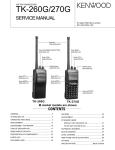
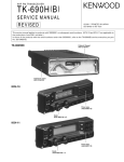
UHF FM TRANSCEIVER
TK-3107
SERVICE MANUAL
© 2000-2 PRINTED IN JAPAN
B51-8572-00(S) 141
M2 version
Antenna
(T90-0694-15)
Knob
(CHANNEL SELECTOR)
(K29-5278-03)
Knob(VOLUME)
(K29-5255-03)
CONTENTS
GENERAL .................................................................. 2
REALIGNMENT ......................................................... 2
DISASSEMBLY FOR REPAIR ................................... 4
CIRCUIT DESCRIPTION ........................................... 5
SEMICONDUCTOR DATA ......................................... 8
DESCRIPTION OF COMPONENTS .......................... 9
PARTS LIST ............................................................. 10
EXPLODED VIEW ................................................... 17
PACKING ................................................................. 18
Cabinet assy
(A02-2448-13)
ADJUSTMENT......................................................... 19
PC BOARD VIEWS
TX-RX UNIT (X57-6030-11) ................................ 23
SCHEMATIC DIAGRAM .......................................... 29
BLOCK DIAGRAM .................................................. 33
LEVEL DIAGRAM ................................................... 35
KNB-15A (Ni-Cd BATTERY) ................................... 36
TK-3107 (16 channels)
SPECIFICATIONS ................................ BACK COVER
TK-3107
GENERAL/REALIGNMENT
3 Getting acquainted
INTRODUCTION
SCOPE OF THIS MANUAL
This manual is intended for use by experienced technicians
familiar with similar types of commercial grade
communications equipment. It contains all required service
information for the equipment and is current as of the
publication data. Changes which may occur after publication
are covered by either Service Bulletins or Manual Revisions.
These are issued as required.
Antenna Microphone
Speaker
Speaker/
microphone
jacks
ORDERING REPLACEMENT PARTS
When ordering replacement parts or equipment
information, the full part identification number should be
included. This applies to all parts : components, kits, or
chassis. If the part number is not known, include the chassis or
kit number of which it is a part, and a sufficient description of
the required component for proper identification.
PERSONAL SAFETY
The following precautions are recommended for personal
safety :
• DO NOT transmit until all RF connectors are verified secure
and any open connectors are properly terminated.
• SHUT OFF and DO NOT operate this equipment near
electrical blasting caps or in an explosive atmosphere.
• This equipment should be serviced by a qualified
technician only.
SERVICE
This radio is designed for easy servicing. Refer to the
schematic diagrams, printed circuit board views, and
alignment procedures contained within.
Destnation
Number of CH
RF power output
M2
16
4W
① PTT (Push-To-Talk) switch
Press this switch, then speak into the microphone to
call a station. Release the switch to receive.
② Monitor key
Press and hold to monitor how busy the current
channel is and to monitor signals being received that
do not contain the matched QT/DQT code.
③ Channel selector
Rotate to select channels 1 ~ 16.
➃ LED indicator
Lights red while transmitting, green while receiving a
signal. Flashes red when the battery voltage is low
while transmitting.
⑤ Power switch/ Volume control
Turn clockwise to switch the transceiver ON. Turn
counterclockwise until a click sounds, to switch the
transceiver OFF. Rotate to adjust the volume level.
PC MODE
REALIGNMENT
Preface
1 Modes
User Mode
PC Mode
Manufacture Mode
MODE
User Mode
PC Mode
FUNCTION
Use this mode for normal operation.
Use this mode, to make various
settings by means of the FPU through
the RS-232C port.
Manufacture Mode Use this mode, to realign the various
settings through the RS-232C port
during manufacture work.
2 How to enter each mode
MODE
User Mode
PC Mode
2
PROCEDURE
Power ON
Connect to the IBM PC compatible
machine and controled by the FPU.
The transceiver is programmed by using a personal
computer, programming interface (KPG-22) and programming
software (KPG-55D).
The programming software can be used with an IBM PC or
compatible. Figure 1 shows the setup of an IBM PC for
programming.
Connenction procedure
1. Connect the TK-3107 to the personal computer with the
interface cable.
2. When data is transmitting from the transceiver the red LED
lights.
When data is received by the transceiver the green LED
lights.
Notes:
• The data stored in the personal computer must match the
Model Name when it is written into the EEPROM.
• Do not press the [PTT] key during data transmission or
reception.
TK-3107
REALIGNMENT
• Programming with IBM PC
• KPG-22 description
If data is transferred to the transceiver from an IBM PC with
the KPG-55D, the destination data (basic radio information)
for each set can be modified. Normally, it is not necessary to
modify the destination data because their values are
determined automatically when the frequency range
(frequency type) is set.
The values should be modified only if necessary.
Data can be programmed into the EEPROM in RS-232C
format via the SP MIC plug.
In this mode the PTT Iine operates as TXD and RXD data lines
respectively.
(PC programming interface cable: Option)
The KPG-22 is required to interface the TK-3107 with the
computer. It has a circuit in its D-subconnector (25-pin) case
that converts the RS-232C Iogic level to the TTL Ievel. The
KPG-22 connects the side panel jacks of the TK-3107 to the
computer's RS-232C serial port.
• Programming software description
The KPG-55D Programming Disk is supplied in 3-1/2" the disk
format. The Software on this disk allows a user to program the
TK-3107 radios via a Programming interface cable (KPG-22).
IBM-PC
KPG-22
Gray
Gray/Black
+
-
+
Gray-XV Shield wire 1.5D-XV Lead wire
KPG-55D
RF Power meter
or SSG
ANT
}
}
SP
MIC
Tuning cable
(E30-3216-05)
Fig. 1
3
TK-3107
DISASSEMBLY FOR REPAIR
Separating the case assembly from the chassis
Separating the chassis from the unit
1. Remove the two knobs ❶ and three round nuts ❷.
2. Remove the two screws ❸.
3. Expand the right and left sides of the bottom of the case
assembly, Iift the chassis, and remove it from the case
assembly ❹.
1. Remove the eleven screws ❻.
2. Remove the solder from the antenna terminal using a
soldering iron then lift the unit off ❼.
3. Remove the two screws ❽ and remove the antenna
connector.
Note : When reassembling the unit in the chassis, be sure to
solder the antenna terminal.
Antenna terminal
4. Taking care not to cut the speaker lead ➎, open the chassis
and case assembly.
Removing the lever
1. Raise the lever on the lower case ➒, insert a small flat
screwdriver into the space between the case and lever,
open the case carefully ➓ and lift the lever off.
Note : Do not force to separate the case from the lever.
Lever knob
Cace assembly
4
TK-3107
CIRCUIT DESCRIPTION
2) First Mixer
1. Frequency configuration
The signal from the RF amplifier is heterodyned with the
first local oscillator signal from the PLL frequency synthesizer
circuit at the first mixer (Q202) to create a 38.85MHz first
intermediate frequency (1st IF) signal. The first IF signal is
then fed through two monolithic crystal filters (MCFs : XF201)
to further remove spurious signals.
The receiver utilizes double conversion. The first IF is
38.85MHz and the second IF is 450kHz. The first local
oscillator signal is supplied from the PLL circuit.
The PLL circuit in the transmitter generates the necessary
frequencies. Fig. 1 shows the frequencies.
3) IF amplifier
CF
450kHz
ANT
The first IF signal is amplified by Q201, and then enters
IC200 (FM processing IC). The signal is heterodyned again
with a second local oscillator signal within IC200 to create a
450kHz second IF signal. The second IF signal is then fed
through a 450kHz ceramic filter (CF200) to further eliminate
unwanted signals before it is amplified and FM detected in
IC200.
MCF
RF
AMP
ANT SW
AF
AMP
IF SYSTEM
SP
38.4MHz
38.85MHz
X3
multiply
TCXO
12.8MHz
RX
PA
AMP
TX
AMP
PLL
VCO
MIC
AMP
MIC
XF201:L71-0522-05
TX
Item
Fig. 1 Frequency configuration
Nominal center frequency
Pass band width
40dB stop band width
Ripple
Insertion loss
Guaranteed attenuation
Terminal impedance
2. Receiver
The receiver is double conversion superheterodyne,
designed to operate in the frequency range of 470 to 490MHz.
The frequency configuration is shown in Fig. 1.
Rating
38.850MHz
±5.0kHz or more at 3dB
±20.0kHz or less
1.0dB or less
4.0dB or less
80dB or more at fo -910kHz
610 / 3PF
1) Front - end RF amplifier
An incoming signal from the antenna is applied to an RF
amplifier (Q203) after passing through a transmit/receive
switch circuit (D102 and D103 are off) and a 3-pole LC filter.
After the signal is amplified (Q203), the signal is filtered by a
band pass filter (a 3-pole LC filter) to eliminate unwanted
signals before it is passed to the first mixer.
The voltage of these diodes are controlled by to track the MPU
(IC403) center frequency of the band pass filter. (See Fig. 2)
CF200:L72-0958-05
Item
Nominal center frequency
6dB band width
50dB band width
Ripple
Insertion loss
Guaranteed attenuation
Terminal impedance
ANT
BPF
L208~L211
D102,D103
RF AMP
Q203
BPF
L214,L203,L204
MIXER
Q202
Rating
450kHz
±6.0kHz or more
±12.5kHz or less
2.0dB or less at fo ±4kHz
6.0dB or less
35.0dB or more at fo ±100kHz
2.0 k
ANT SW
TUNE
APC
4) AF amplifier
IC403
MPU
1st Local OSC
(PLL)
CF200
MCF
XF201
IF AMP
Q201
AF PA AMP
IC302
IF, MIX, DET
IC200
TCXO
X3
multiply
Q1
AF AMP
LPF, HPF
IC300
SP
The recovered AF signal obtained from IC200 is amplified
by IC300 (1/4), filtered by the IC300 low-pass filter (2/4) and
IC300 high-pass filter (3/4) and (4/4), and de-emphasized by
R303 and C306. The AF signal is then passed through a
WIDE/NARROW switch (Q303). The processed AF signal
passes through an AF volume control and is amplified to a
sufficient level to drive a loud speaker by an AF power
amplifier (IC302).
WIDE/NARROW SW
Q303
Fig. 2 Receiver section configuration
5
TK-3107
CIRCUIT DESCRIPTION
5) Squelch
6) Receive signaling
Part of the AF signal from the IC enters the FM IC again,
and the noise component is amplified and rectified by a filter
and an amplifier to produce a DC voltage corresponding to the
noise level.
The DC signal from the FM IC goes to the analog port of the
microprocessor (IC403). IC403 determines whether to output
sounds from the speaker by checking whether the input
voltage is higher or lower than the preset value.
To output sounds from the speaker, IC403 sends a high signal
to the MUTE and AFCO Iines and turns IC302 on through
Q302, Q304, Q305, Q306 and Q307.(See Fig. 3)
QT/DQT
300 Hz and higher audio frequencies of the output signal
from IF IC are cut by a low-pass filter (IC301). The resulting
signal enters the microprocessor (IC403). IC403 determines
whether the QT or DQT matches the preset value, and
controls the MUTE and AFCO and the speaker output sounds
according to the squelch results.
IC300
FM IF IC IC200
AF AMP
IF AMP
DET
LPF
HPF
Q302
SW
IC302
AF PA AMP
Q307
SW
SP
HPF
AMP
DET
Q304, 305, 306
SW
5
QT/DQT
Q303
W/N SW
TI
67
62
AFCO
MUTE
BUSY
6
IC301
LPF
IC403
MPU
Fig. 3 AF Amplifier and squelch
3. PLL frequency synthesizer
The PLL circuit generates the first local oscillator signal for
reception and the RF signal for transmission.
1) PLL
2) VCO
The frequency step of the PLL circuit is 5 or 6.25kHz.
A 12.8MHz reference oscillator signal is divided at IC1 by a fixed
counter to produce the 5 or 6.25kHz reference frequency. The
voltage controlled oscillator (VCO) output signal is buffer
amplified by Q6, then divided in IC1 by a dual-module
programmable counter . The divided signal is compared in phase
with the 5 or 6.25kHz reference signal in the phase comparator in
IC1. The output signal from the phase comparator is filtrered
through a low-pass filter and passed to the VCO to control the
oscillator frequency. (See Fig.4)
The operating frequency is generated by Q4 in transmit
mode and Q3 in receive mode. The oscillator frequency is
controlled by applying the VCO control voltage, obtained from
the phase comparator, to the varactor diodes (D2 and D4 in
transmit mode and D1 and D3 in receive mode). The T/R pin is
set high in receive mode causing Q5 and Q7 to turn Q4 off,
and turn Q3 on . The T/R pin is set low in transmit mode. The
outputs from Q3 and Q4 are amplified by Q6 and sent to the
buffer amplifiers.
PLL IC IC1
D2, 4
5kHz/6.25kHz
Q4
TX VCO
Q2
RF AMP
I/N
LPF
Q6
BUFF AMP
PLL DATA
PHASE
COMPARATOR
REF OSC
CHARGE
PUMP
D1, 3
5kHz/6.25kHz
12.8MHz
Fig. 4 PLL circuit
6
Q3
RX VCO
Q5, 7
T/R SW
I/M
TK-3107
CIRCUIT DESCRIPTION
3) UNLOCK DETECTOR
ANT
If a pulse signal appears at the LD pin of IC1, an unlock
condition occurs, and the DC voltage obtained from D7, R6,
and C1 causes the voltage applied to the UL pin of the
microprocessor to go low. When the microprocessor detects
this condition, the transmitter is disabled, ignoring the push-totalk switch input signal. ( See Fig.5)
AMP
Q101,Q102
DRIVE AMP
Q105
FINAL AMP
Q107
LPF
ANT SW
D101
5T
5C
APC
Q109
DET
SW
IC100
R6
IC1
Q103, Q104
B SW
IC403
D7
ANT SW
LD
B
UL
Q106
5T
D102,103
SW
C1
PLL IC
APC
MPU
Q108
TH102
Fig. 5 Unlock detector circuit
SW
Q110
4. Transmitter
1) Transmit audio
The modulation signal from the microphone is amplified by
IC500 (1/2), passes through a preemphasis circuit, and
amplified by the other IC500 (1/2) to perform IDC operation.
The signal then passes through a low-pass filter (splatter fiIter)
(Q501 and Q502) and cuts 3kHz and higher frequencies. The
resulting signal goes to the VCO through the VCO modulation
terminal for direct FM modulation. (See Fig. 6)
2) QT/DQT encoder
A necessary signal for QT/DQT encoding is generated by
IC403 and FM-modulated to the PLL reference signal. Since
the reference OSC does not modulate the loop characteristic
frequency or higher, modulation is performed at the VCO side
by adjusting the balance. (See Fig. 6)
IC500 (1/2)
MIC
PREEMPHASIS
AMP
Q501, 502
VR501
LPF
IC500 (1/2)
MAX
(SPLATTER FILTER) DEV
IDC
VR500
BALANCE
Q503
SW
IC403
5T
Fig. 7 APC system
5) APC
The automatic power control (APC) circuit stabilizes the
transmitter output power at a predetermined level by sensing
the drain current of the final amplifier Field Effect Transistor
(FET) . The voltage comparator, IC100 (2/2), compares the
voltage obtained from the above drain current with a reference
voltage which is set using the microprocessor. An APC
voltage proportional to the difference between the sensed
voltage and the reference voltage appears at the output of
IC100 (1/2). This output voltage controls the gate of the FET
power amplifier, which keeps the transmitter output power
constant. The transmitter output power can be varied by the
microprocessor which in turn changes the reference voltage
and hence, the output power.
D5, Q4
VCO
MIC
RX
SW
5T
6) Terminal protection circuit
When the thermistor (TH102) reaches about 80˚C, the
protection circuit turns on Q110 to protect transmitting final
amplifier (Q107) from the over heating.
X1, IC1
TO
QT/DQT
MUTE
REFERENCE
OSC
(TCXO)
Fig. 6 Transmit audio QT/DQT
3) VCO and RF amplifier
The transmit signal obtained from the VCO buffer amplifier
Q100, is amplified by Q101 and Q102. This amplified signal is
passed to the power amplifier, Q105 and Q107, which
consists of a 2-stage FET amplifier and is capable of
producing up to 4W of RF power. (See Fig.7)
4) ANT switch and LPF
The RF amplifier output signal is passed through a lowpass filter network and a transmit/receive switching circuit
before it is passed to the antenna terminal. The transmit/
receive switching circuit is comprised of D101, D102 and
D103. D102 and D103 are turned on (conductive) in transmit
mode and off (isolated) in receive mode.
5. Power supply
A 5V reference power supply [5M] for the control circuit is
derived from an internal battery. This reference is used to
provide a 5V supply in transmit mode [5T], a 5V supply in
receive mode [5R], and a 5V supply common in both modes
[5C] based on the control signal sent from the microprocessor.
6. Control system
The IC403 CPU operates at 7.37MHz . This oscillator has a
circuit that shifts the frequency according to the EEPROM
data.
7
TK-3107
SEMICONDUCTOR DATA
Microprocessor: M38267M8L241GP (IC403)
Pin No. I/O
8
Port Name
1
2
3
O
O
I
VC1
VC2
NC
4
I
TIBI
5
6
7
8
9
I
I
l
l
O
TI
BUSY
BATT
NC
VCCN
10
O
APC/TUNE
11
12
13
14
15
16
17
18
I
I
l
l
O
O
l
I
NC
NC
NC
NC
BEEP
TO
NC
PTT
19
O
TXD
20
I
RXD
21
22
23
24
25
26
27
28
29
30
31
32
33
34
35
36
37
38
39
40
l
I
I
I
I
I
l
l
l
l
l
l
I
I
O
l
O
I
O
O
NC
SELF
MONl
NC
NC
NC
NC
ENC3
ENC2
ENC1
ENC0
INTO
RST
NC
NC
XIN
XOUT
VSS
SHIFT
PABC
41
O
WNRC
42
43
44
45
46
47
48
49
50
51
52
53
54
55
56
57
58
O
l
l
I
l
l/O
O
I
l
I
I
l
I
O
O
O
O
WNTC
NC
NC
NC
NC
SDA
SCL
UL
NC
NC
NC
NC
NC
DT
CK
NC
LE
Function
NC
NC
NC
QT/DQT external circuit center
point input
QT/DQT signal input
Busy input
Battery voltage detection
NC
Frequency regulation output
TX : Auto power control D/A output
RX : BPF tuning D/A output
NC
NC
NC
NC
Beep output
QT/DQT output
NC
[PTT] key input Connected to RXD
RS-232C output Connected to SP/
MIC test(REM)
RS-232C input Connected to [PTT]
line
NC
Self program
L : disable
[MONl] key input
NC
NC
NC
NC
Encode input (channel select)
Encode input (channel select)
Encode input (channel select)
Encode input (channel select)
Power detection control
Reset input
NC
NC
7.3728MHz oscillator
7.3728MHz oscillator
GND
Beat shift
H : shift on
Final supply
H : on
Audio reference sensitivity
L : narrow
MAX Dev. Control
Narrow: H
NC
NC
NC
NC
EEPROM data line
EEPROM clock line
PLL unlock detection pin L : unlock
NC
NC
NC
NC
NC
Common data output
Common clock output
NC
PLL IC enable
H : Iatches
Pin No. I/O
Port Name
59
60
O
O
NC
NC
61
O
5MC
62
63
64
65
66
O
O
O
O
O
AFCO
RX
GLED
RLED
SAVE
67
O
MUTE
68
O
5RC
69
O
5TC
70
71
72
73
74
75
76
77
78
79
80
81
82
83
84
85
86
87
88
89
O
O
O
O
O
O
O
O
O
O
O
O
O
O
O
O
O
O
O
l
NC
NC
NC
NC
NC
NC
NC
NC
NC
NC
NC
NC
NC
NC
NC
NC
NC
NC
NC
VCC
90
l
VREF
91
l
AVSS
92
93
94
95
96
97
98
99
100
O
O
O
O
I
l
I
I
I
NC
NC
NC
NC
NC
NC
NC
NC
NC
Function
NC
NC
Control of power supply (5M) for
everything except the
microcomputer and EEPROM L
: Power supply ON
AF amp power suppIy
H : ON
TX/RX VCO select
H : RX
Green LED control
H : Lit
RED LED control
H : Lit
Save control
H : Save off
Mute control
H : Mic mute
L : AF mute
Reception power suppIy control
L : on
Transmission power suppIy control
H : on
NC
NC
NC
NC
NC
NC
NC
NC
NC
NC
NC
NC
NC
NC
NC
NC
NC
NC
NC
Microcomputer power supply, 5V input
A/D conversion reference voltage ;
connected to Vcc
A/D converter power supply ;
connected to Vss
NC
NC
NC
NC
NC
NC
NC
NC
NC
FET : 2SK2596(Q105)
Absolute Maximum Ratings (Ta=25°C)
Item
Rating
VDSS
17V
VGSS
±10V
ID
0.4A
Pch*
Tch
3W
150°C
*Tc=25°C
Tstg
-45~+150°C
FET : 2SK2595(Q107)
Absolute Maximum Ratings (Ta=25°C)
Item
Rating
VDS
17V
VGSS
±10V
ID
1.1A
Pch*
Tch
20W
150°C
*Tc=25°C
Tstg
-45~+150°C
TK-3107
DESCRIPTION OF COMPONENTS
Ref No.
IC1
Semiconductor
IC
IC100
IC200
IC300
IC301
IC302
IC400
IC401
IC402
IC403
IC404
IC500
Q1
Q2
Q3
Q4
Q5
Q6
Q7
Q8
Q100
Q101
Q102
Q103
Q104
Q105
Q106
Q107
Q108,109
IC
IC
IC
IC
IC
IC
IC
IC
IC
IC
IC
TRANSISTOR
TRANSISTOR
FET
TRANSISTOR
FET
TRANSISTOR
TRANSISTOR
TRANSISTOR
TRANSISTOR
TRANSISTOR
FET
FET
TRANSISTOR
FET
FET
FET
TRANSISTOR
Q110
TRANSISTOR
Q200
Q201
Q202
Q203
Q300
Q302
Q303-306
Q307
Q400-402
Q403
Q404
Q405
Q406-408
Q500
Q501,502
Q503
Q504
TRANSISTOR
TRANSISTOR
FET
FET
TRANSISTOR
FET
TRANSISTOR
FET
TRANSISTOR
TRANSISTOR
TRANSISTOR
FET
TRANSISTOR
FET
TRANSISTOR
TRANSISTOR
TRANSISTOR
VARIABLE CAPACITANCE
D1-4
DIODE
VARIABLE CAPACITANCE
D5
DIODE
D6
DIODE
D7
DIODE
D100 DIODE
D101-103 DIODE
D200 DIODE
VARIABLE CAPACITANCE
D201-205
DIODE
D300 DIODE
D400 LED
D401 LED
D500 DIODE
D501 DIODE
D502 DIODE
Description
PHASE LOCKED LOOP
SYSTEM
AUTOMATIC POWER CONTROL
IF SYSTEM
AUDIO AMP ACTIVE FILTER
ACTIVE FILTER
AUDIO POWER AMP
RESET SWITCH
EEPROM
VOLTAGE DETECT
MICRO PROCESSOR
VOLTAG E REGULATER
MIC AMP/LIMITER
TRIPLER
RF AMP
VCO RX
VCO TX
DC SWITCH
RF BUFFER AMP
DC SWITCH
RIPPLE FILTER
RF AMP
TX PRE-DRIVE
TX DRIVE
DC SWITCH
DC SWITCH
TX DRIVE
DC SWITCH
TX FAINAL
DC SWITCH
TEMPERATURE
PROTECTION SWITCH
DC SWITCH
IF AMP
MIXER
MIXER RF AMP
ACTIVE FILTER
AUDIO MUTE SWITCH
DC SWITCH
AUDIO MUTE SWITCH
DC SWITCH
BEAT SHIFT SWITCH
DC SWITCH
DC SWITCH
DC SWITCH
DC SWITCH
ACTIVE FILTER
MIC MUTE/ AGC
DC SWITCH
FREQ. CONTROL
TX MODULATION
CURRENT STEERING
UNLOCKDETECT
RF SWITCH
ANTENNA SWITCH
RF SWITCH
BPF TUNING
LIMITER
TX
BUSY
AGC DETECT
MIC MUTE/AGC SWITCH
REVERSE PROTECTION
9
TK-3107
PARTS LIST
TK-260
10
:K, K2
TK-3107
PARTS LIST
∗ New Parts. ! indicates safety critical components.
Parts without Parts No. are not supplied.
Les articles non mentionnes dans le Parts No. ne sont pas fournis.
Teile ohne Parts No. werden nicht geliefert.
TX-RX UNIT (X57-6030-11)
TK-3107
Ref. No.
New
Address parts
Parts No.
Description
TK-3107
1
2
1A
3B
3
4
5
-
6
7
Destination
Ref. No.
New
Address parts
Parts No.
Description
C5
C6
C7
C9
C10
C92-0507-05
CC73GCH1H101J
CK73GB1H471K
CC73GCH1H100D
CC73GCH1H470J
CHIP-TAN
CHIP C
CHIP C
CHIP C
CHIP C
4.7UF
100PF
470PF
10PF
47PF
6.3WV
J
K
D
J
C92-0001-05
CC73GCH1H100D
C92-0004-05
CC73GCH1H680J
CK73GB1H331K
CHIP-C
CHIP C
CHIP-TAN
CHIP C
CHIP C
0.1UF
10PF
1.0UF
68PF
330PF
35WV
D
16WV
J
K
A02-2448-13
A82-0034-03
CABINET ASSY
REAR PANEL
B09-0351-03
B62-1164-10
B72-1945-04
CAP
INSTRUCTION MANUAL
MODEL NAME PLATE
2B
3B
E04-0413-05
E23-1183-04
RF COAXIAL RECEPTACLE(SMA)
RELAY TERMINAL(BATT-)
C12
C14
C15
C16
C17
8
9
10
-
1A
2B
2B
-
G01-0881-04
G11-2583-04
G11-2588-04
G13-1709-04
G13-1763-04
COIL SPRING(BATT RELEASE)
SHEET
RUBBER SHEET(CHASSIS)
CUSHION(VOL)
CUSHION(CHASSIS-BATT)
C18
C19,20
C23
C24
C25
C92-0001-05
CK73GB1H103K
C92-0560-05
CK73GB1H103K
CK73GB1H471K
CHIP-C
CHIP C
CHIP-TAN
CHIP C
CHIP C
0.1UF
0.010UF
10UF
0.010UF
470PF
35WV
K
6.3WV
K
K
11
12
13
14
3A
2B
2A
2A
G13-1834-04
G53-0791-03
G53-0842-13
G53-0860-04
CUSHION(BATT-)
PACKING(SP/MIC PLUG)
PACKING(SPEAKER)
PACKING(SIDE)
C26
C27
C28
C29
C30
CC73GCH1H121J
CK73GB1H471K
CC73GCH1H330J
CC73GCH1H020C
CK73GB1H102K
CHIP C
CHIP C
CHIP C
CHIP C
CHIP C
120PF
470PF
33PF
2.0PF
1000PF
J
K
J
C
K
15
16
17
18
-
H12-3037-02
H25-0085-04
H25-2012-04
H52-1560-02
PACKING FIXTURE
PROTECTION BAG (100/200/0.07)
PROTECTION BAG (75/100/0.08)
ITEM CARTON CASE
19
20
21
22
-
1A
2B
3B
-
J19-1572-04
J19-5344-03
J21-4493-04
J29-0624-03
J82-0059-05
HOLDER(BATT RELEASE)
HOLDER(VOL/ENC)
SP/MIC HOLDER
BELT HOOK
FPC
C31
C34
C35
C36
C37
CC73GCH1H101J
CC73GCH1H330J
CC73GCH1H060B
CC73GCH1H080B
CC73GCH1H150J
CHIP C
CHIP C
CHIP C
CHIP C
CHIP C
100PF
33PF
6.0PF
8.0PF
15PF
J
J
B
B
J
23
24
25
26
27
1B
1A
1A
1B
1A
K29-5255-03
K29-5274-03
K29-5275-03
K29-5278-03
K29-5337-03
KNOB(VOL)
BUTTON KNOB(MONI)
BUTTON KNOB(PTT)
KNOB(ENC)
LEVER KNOB(BATT RELEASE)
C38
C39
C40
C41
C42
CC73GCH1H020B
CC73GCH1H080B
CC73GCH1H0R5B
CC73GCH1H050B
CC73GCH1H130J
CHIP C
CHIP C
CHIP C
CHIP C
CHIP C
2.0PF
8.0PF
0.5PF
5.0PF
13PF
B
B
B
B
J
A
B
C
D
E
2B
1B
1B
3A
3B
N09-2319-05
N14-0581-04
N14-0582-14
N30-2606-46
N79-2035-46
BINDING HEAD SCREW(SMA)
CIRCULAR NUT(VOL)
CIRCULAR NUT(SMA)
PAN HEAD MACHINE SCREW
PAN HEAD TAPTITE SCREW
C43
C44
C45
C46
C47
CK73GB1H102K
CC73GCH1H050B
CC73GCH1H060B
CK73GB1H471K
CC73GCH1H010B
CHIP C
CHIP C
CHIP C
CHIP C
CHIP C
1000PF
5.0PF
6.0PF
470PF
1.0PF
K
B
B
K
B
F
G
2A,2B
-
N83-2005-46
N99-0396-05
PAN HEAD TAPTITE SCREW
SCREW SET
C48
C49
C51
C52
C53
CK73GB1H471K
CC73GCH1H0R5B
CC73GCH1H680J
CK73GB1H471K
CC73GCH1H060D
CHIP C
CHIP C
CHIP C
CHIP C
CHIP C
470PF
0.5PF
68PF
470PF
6.0PF
K
B
J
K
D
-
-
R31-0624-05
VARIABLE RESISTOR
-
-
S60-0420-05
ROTARY SWITCH
C54
C55
C56
C100
C101-103
CC73GCH1H030B
CK73GB1H471K
C92-0507-05
CC73GCH1H220J
CK73GB1H471K
CHIP C
CHIP C
CHIP-TAN
CHIP C
CHIP C
3.0PF
470PF
4.7UF
22PF
470PF
B
K
6.3WV
J
K
SP
ANT
1A
T07-0369-05
T90-0694-15
SPEAKER
WHIP ANTENNA
C104
C105
C106,107
C108
C109,110
CK73GB1C104K
CC73GCH1H060D
CK73GB1H471K
CC73GCH1H070D
CK73GB1H471K
CHIP C
CHIP C
CHIP C
CHIP C
CHIP C
0.10UF
6.0PF
470PF
7.0PF
470PF
K
D
K
D
K
C111
C112
C113
CC73GCH1H060D
CK73GB1H471K
CK73GB1C104K
CHIP C
CHIP C
CHIP C
6.0PF
470PF
0.10UF
D
K
K
∗
∗
∗
TX-RX UNIT (X57-6030-11) • M2
D400
D401
C1
C2,3
C4
TK-260
B30-2156-05
B30-2157-05
CK73GB1C104K
CC73GCH1H101J
CK73GB1C104K
:K, K2
LED(RED)
LED(YELLOW)
CHIP C
0.10UF
CHIP C
100PF
CHIP C
0.10UF
K
J
K
Destination
11
TK-3107
PARTS LIST
TX-RX UNIT (X57-6030-11)
New
Ref. No. Address parts
Parts No.
Description
Destination
New
Ref. No. Address parts
Parts No.
Description
C114,115
C116
C118
C119
C120,121
CK73GB1H471K
CK73GB1H102K
CC73GCH1H270G
CK73GB1H102K
CK73GB1H471K
CHIP C
CHIP C
CHIP C
CHIP C
CHIP C
470PF
1000PF
27PF
1000PF
470PF
K
K
G
K
K
C226
C227
C228
C229
C231,232
CC73GCH1H0R5B
CC73GCH1H070B
CC73GCH1H080B
CK73GB1H471K
CK73GB1H471K
CHIP C
CHIP C
CHIP C
CHIP C
CHIP C
0.5PF
7.0PF
8.0PF
470PF
470PF
B
B
B
K
K
C123
C125
C126
C127
C128
CK73GB1H102K
CK73GB1H471K
CK73FB1A105K
C92-0565-05
CK73GB1H103K
CHIP C
CHIP C
CHIP C
CHIP-TAN
CHIP C
1000PF
470PF
1.0UF
6.8UF
0.010UF
K
K
K
10WV
K
C233
C234
C235
C236
C237
CC73GCH1H0R3B
CC73GCH1H0R5B
CC73GCH1H030B
CC73GCH1H2R5B
CK73GB1H471K
CHIP C
CHIP C
CHIP C
CHIP C
CHIP C
0.3PF
0.5PF
3.0PF
2.5PF
470PF
B
B
B
B
K
C129
C130
C131
C132
C134
CK73GB1H471K
CC73FCH1H220G
CK73GB1C104K
CK73GB1H471K
CC73GCH1H101J
CHIP C
CHIP C
CHIP C
CHIP C
CHIP C
470PF
22PF
0.10UF
470PF
100PF
K
G
K
K
J
C238
C239
C252
C253,254
C255
CC73GCH1H0R5B
CC73GCH1H2R5B
CC73GCH1H4R5B
CK73GB1H471K
CC73GCH1H3R5B
CHIP C
CHIP C
CHIP C
CHIP C
CHIP C
0.5PF
2.5PF
4.5PF
470PF
3.5PF
B
B
B
K
B
C135
C136
C138
C139
C141
CC73GCH1H010C
CC73GCH1H060B
CC73GCH1H101J
CK73GB1H471K
CK73GB1H471K
CHIP C
CHIP C
CHIP C
CHIP C
CHIP C
1.0PF
6.0PF
100PF
470PF
470PF
C
B
J
K
K
C256
C257
C258
C259
C300
CK73GB1C104K
CK73GB1H471K
CK73GB1C104K
CC73GCH1H4R5B
CK73GB1H822K
CHIP C
CHIP C
CHIP C
CHIP C
CHIP C
0.10UF
470PF
0.10UF
4.5PF
8200PF
K
K
K
B
K
C142
C143
C144
C145
C147
CC73GCH1H030B
CK73GB1H471K
CC73GCH1H020B
CK73GB1H471K
CC73GCH1H010B
CHIP C
CHIP C
CHIP C
CHIP C
CHIP C
3.0PF
470PF
2.0PF
470PF
1.0PF
B
K
B
K
B
C301
C302,303
C304
C305
C306
CK73GB1E183K
CK73GB1C104K
C92-0560-05
CK73GB1H103J
CK73GB1C473K
CHIP C
CHIP C
CHIP-TAN
CHIP C
CHIP C
0.018UF
0.10UF
10UF
0.010UF
0.047UF
K
K
6.3WV
J
K
C149
C150
C151
C153
C154
CC73GCH1H010B
CC73GCH1H4R5B
CC73GCH1H1R5B
CC73GCH1H2R5B
CC73GCH1H010B
CHIP C
CHIP C
CHIP C
CHIP C
CHIP C
1.0PF
4.5PF
1.5PF
2.5PF
1.0PF
B
B
B
B
B
C307
C308
C309
C311
C312
C92-0560-05
CK73GB1H562K
CK73GB1H103J
C92-0560-05
CK73GB1H103J
CHIP-TAN
CHIP C
CHIP C
CHIP-TAN
CHIP C
10UF
5600PF
0.010UF
10UF
0.010UF
6.3WV
K
J
6.3WV
J
C155
C156
C157
C165
C200
CC73GCH1H1R5B
CK73GB1C104K
CK73GB1H471K
CK73GB1H471K
C92-0560-05
CHIP C
CHIP C
CHIP C
CHIP C
CHIP-TAN
1.5PF
0.10UF
470PF
470PF
10UF
B
K
K
K
6.3WV
C313
C314
C316
C318
C319
CK73FB1A105K
CK73GB1H102K
CK73GB1H103J
CK73GB1C333J
CK73GB1C473J
CHIP C
CHIP C
CHIP C
CHIP C
CHIP C
1.0UF
1000PF
0.010UF
0.033UF
0.047UF
K
K
J
J
J
C201
C202
C203
C204
C205,206
CK73GB1H103K
CC73GCH1H100D
CK73GB1H471K
CK73GB1H472K
CC73GCH1H221J
CHIP C
CHIP C
CHIP C
CHIP C
CHIP C
0.010UF
10PF
470PF
4700PF
220PF
K
D
K
K
J
C320,321
C322
C327
C330
C331
CK73GB1C333J
CK73FB1E104K
CK73GB1C104K
CC73GCH1H101J
CK73FB1C474K
CHIP C
CHIP C
CHIP C
CHIP C
CHIP C
0.033UF
0.10UF
0.10UF
100PF
0.47UF
J
K
K
J
K
C207
C208
C209
C210
C211
CK73GB1C104K
CC73GCH1H270J
CK73GB1C104K
CK73GB1H103K
CK73GB1C104K
CHIP C
CHIP C
CHIP C
CHIP C
CHIP C
0.10UF
27PF
0.10UF
0.010UF
0.10UF
K
J
K
K
K
C332
C333
C334
C335
C336
C92-0560-05
CK73GB1A474K
CC73GCH1H221J
CK73GB1C473K
CK73GB1H103K
CHIP-TAN
CHIP C
CHIP C
CHIP C
CHIP C
10UF
0.47UF
220PF
0.047UF
0.010UF
6.3WV
K
J
K
K
C212
C213
C214
C215
C217
CC73GCH1H330J
CK73GB1C104K
CK73GB1H103K
CC73GCH1H130J
CK73GB1H103K
CHIP C
CHIP C
CHIP C
CHIP C
CHIP C
33PF
0.10UF
0.010UF
13PF
0.010UF
J
K
K
J
K
C337
C338
C400
C402-404
C406
C92-0665-05
CC73GCH1H560J
CK73GB1C104K
CK73GB1H471K
CK73GB1H471K
TANTAL
CHIP C
CHIP C
CHIP C
CHIP C
100UF
56PF
0.10UF
470PF
470PF
6.3WV
J
K
K
K
C218
C219
C220,221
C222
C223
CK73GB1H471K
CC73GCH1H180J
CK73GB1H103K
CC73GCH1H050B
CC73GCH1H020C
CHIP C
CHIP C
CHIP C
CHIP C
CHIP C
470PF
18PF
0.010UF
5.0PF
2.0PF
K
J
K
B
C
C407
C408
C409
C410,411
C412
CK73GB1H102K
C92-0560-05
CC73GCH1H030B
CK73GB1H471K
CC73GCH1H100D
CHIP C
CHIP-TAN
CHIP C
CHIP C
CHIP C
1000PF
10UF
3.0PF
470PF
10PF
K
6.3WV
B
K
D
C224
CK73GB1H471K
CHIP C
470PF
K
C413
CK73GB1H102K
CHIP C
1000PF
K
12
400~420Hz : C5
450~470Hz : C6
Destination
TK-3107
PARTS LIST
TX-RX UNIT (X57-6030-11)
New
Ref. No. Address parts
Parts No.
Description
Destination
New
Ref. No. Address parts
Parts No.
Description
Destination
C414
C415
C416
C417
C418
CK73GB1H471K
CC73GCH1H100D
CK73GB1H471K
CK73EF1C105Z
CK73GB1H103K
CHIP C
CHIP C
CHIP C
CHIP C
CHIP C
470PF
10PF
470PF
1.0UF
0.010UF
K
D
K
Z
K
L2
L4
L5
L6
L7
L40-1005-85
L40-4781-86
L40-5681-86
L40-1875-77
L92-0140-05
SMALL FIXED INDUCTOR(10UH)
SMALL FIXED INDUCTOR(0.47UH)
SMALL FIXED INDUCTOR(0.56UH)
SMALL FIXED INDUCTOR(18NH)
FERRITE CHIP
C420-422
C423
C424
C425
C427
CK73GB1H103K
CK73GB1C104K
CK73FB1A105K
CK73GB1H103K
CK73GB1H471K
CHIP C
CHIP C
CHIP C
CHIP C
CHIP C
0.010UF
0.10UF
1.0UF
0.010UF
470PF
K
K
K
K
K
L8
L9
L10
L11
L12
L40-1085-77
L40-3391-86
L92-0140-05
L40-3391-86
L40-1085-77
SMALL FIXED INDUCTOR(100NH)
SMALL FIXED INDUCTOR(3.3UH)
FERRITE CHIP
SMALL FIXED INDUCTOR(3.3UH)
SMALL FIXED INDUCTOR(100NH)
C429,430
C500,501
C502
C503
C504
CK73FB1A105K
CK73GB1C273K
CK73GB1H392K
CK73GB1C333K
C92-0507-05
CHIP C
CHIP C
CHIP C
CHIP C
CHIP-TAN
1.0UF
0.027UF
3900PF
0.033UF
4.7UF
K
K
K
K
6.3WV
L13,14
L15
L16,17
L19
L20
L33-0744-05
L40-1085-77
L40-2285-38
L92-0140-05
L40-3391-86
SMALL FIXED INDUCTOR(23NH)
SMALL FIXED INDUCTOR(100NH)
SMALL FIXED INDUCTOR(220NH)
FERRITE CHIP
SMALL FIXED INDUCTOR(3.3UH)
C505
C506
C507
C508
C509
CK73FB1A105K
CK73GB1H471K
C92-0587-05
CK73GB1H103K
CK73GB1H332K
CHIP C
CHIP C
CHIP-TAN
CHIP C
CHIP C
1.0UF
470PF
2.2UF
0.010UF
3300PF
K
K
4WV
K
K
L21
L100
L101
L102
L103
L40-2275-77
L40-2275-77
L40-1875-77
L40-1575-77
L92-0140-05
SMALL FIXED INDUCTOR(22NH)
SMALL FIXED INDUCTOR(22NH)
SMALL FIXED INDUCTOR(18NH)
SMALL FIXED INDUCTOR(15NH)
FERRITE CHIP
C510
C511
C512
C513
C514
CC73GCH1E681J
CK73GB1C473K
CK73GB1H332K
CC73GCH1E681J
CK73GB1C473K
CHIP C
CHIP C
CHIP C
CHIP C
CHIP C
680PF
0.047UF
3300PF
680PF
0.047UF
J
K
K
J
K
L104
L105
L106
L107
L109
L40-1098-76
L92-0149-05
L34-4551-05
L92-0149-05
L40-2285-54
SMALL FIXED INDUCTOR(1UH)
FERRITE CHIP
AIR-CORE COIL
FERRITE CHIP
SMALL FIXED INDUCTOR(220NH)
C515
C516
C517
C518
C519
CK73GB1H103K
CC73GCH1H100D
CK73GB1H471K
CK73GB1E223J
C92-0507-05
CHIP C
CHIP C
CHIP C
CHIP C
CHIP-TAN
0.010UF
10PF
470PF
0.022UF
4.7UF
K
D
K
J
6.3WV
L110
L112
L113
L114
L118
L34-4547-05
L34-4547-05
L34-4547-05
L34-4546-05
L40-1092-81
AIR-CORE COIL
AIR-CORE COIL
AIR-CORE COIL
AIR-CORE COIL
SMALL FIXED INDUCTOR
C520
C521
C522
C523
C524
CK73GB1E223J
CK73GB1H102K
CK73FB1E104K
C92-0587-05
CK73GB1C273K
CHIP C
CHIP C
CHIP C
CHIP-TAN
CHIP C
0.022UF
1000PF
0.10UF
2.2UF
0.027UF
J
K
K
4WV
K
L119
L200
L201
L202
L203,204
L40-2263-77
L40-3385-85
L40-5685-85
L40-2275-77
L34-4546-05
SMALL FIXED INDUCTOR(2.2NH)
SMALL FIXED INDUCTOR(0.33UH)
SMALL FIXED INDUCTOR(0.56UH)
SMALL FIXED INDUCTOR(22NH)
AIR-CORE COIL
C525
C526
C527
C528
C529
CK73GB1C104K
CK73GB1H471K
C92-0560-05
CK73GB1H471K
CK73FB1H471K
CHIP C
CHIP C
CHIP-TAN
CHIP C
CHIP C
0.10UF
470PF
10UF
470PF
470PF
K
K
6.3WV
K
K
L206
L207
L208-211
L212
L212
L40-1875-77
L40-3375-77
L34-4546-05
L34-4554-05
L34-4585-05
SMALL FIXED INDUCTOR(18NH)
SMALL FIXED INDUCTOR(33NH)
AIR-CORE COIL
COIL
COIL
C530,531
C532
TC1
TC2
TC201
CC73GCH1H221J
CK73GB1H471K
C05-0383-05
C05-0384-05
C05-0383-05
CHIP C
220PF
J
CHIP C
470PF
K
CERAMIC TRIMMER CAP(6PF)
CERAMIC TRIMMER CAP(10PF)
CERAMIC TRIMMER CAP(6PF)
L214
L400
L401
L402,403
L500
L34-4546-05
L40-2281-86
L92-0140-05
L40-2281-86
L92-0140-05
AIR-CORE COIL
SMALL FIXED INDUCTOR(0.22UH)
FERRITE CHIP
SMALL FIXED INDUCTOR(0.22UH)
FERRITE CHIP
TC202,203
C05-0369-05
CERAMIC TRIMMER CAP
CN400
J500
F500
F500
E23-1005-04
E40-5998-05
E11-0457-05
F53-0130-05
F53-0217-05
RELAY TERMINAL
PIN ASSY
PHONE JACK
FUSE
FUSE
L501,502
X1
X400
XF201
L92-0149-05
L77-1756-05
L77-1761-05
L71-0522-05
FERRITE CHIP
TCXO(12.8MHZ)
CRYSTAL RESONATOR(7.3728MHZ)
MCF(38.85MHZ)
N78-2640-46
PAN HEAD TAPTITE SCREW
G53-0862-04
J19-1571-04
J30-1249-04
L72-0958-05
L92-0140-05
PACKING
HOLDER
SPACER
CERAMIC FILTER
FERRITE CHIP
R90-0724-05
RK73GB1J102J
RK73GB1J100J
RK73GB1J102J
RK73GB1J561J
MULTI-COMP1KX4
CHIP R
1.0K
CHIP R
10
CHIP R
1.0K
CHIP R
560
34
2B
CF200
L1
400~420Hz : C5
450~470Hz : C6
CP1
R1,2
R3
R4
R5
J
J
J
J
1/16W
1/16W
1/16W
1/16W
13
TK-3107
PARTS LIST
TX-RX UNIT (X57-6030-11)
New
Ref. No. Address parts
Parts No.
Description
Destination
New
Ref. No. Address parts
Parts No.
Description
Destination
R6
R7
R8
R9
R10
RK73GB1J154J
RK73GB1J561J
RK73GB1J334J
RK73GB1J272J
RK73GB1J222J
CHIP R
CHIP R
CHIP R
CHIP R
CHIP R
150K
560
330K
2.7K
2.2K
J
J
J
J
J
1/16W
1/16W
1/16W
1/16W
1/16W
R139
R140
R141
R142
R143
RK73GB1J271J
RK73GB1J103J
RK73GB1J473J
RK73GB1J105J
R92-1252-05
CHIP R
CHIP R
CHIP R
CHIP R
CHIP R
270
10K
47K
1.0M
0 OHM
J
J
J
J
R11
R12
R13
R14
R15
RK73GB1J473J
RK73GB1J274J
RK73GB1J221J
RK73GB1J101J
RK73GB1J103J
CHIP R
CHIP R
CHIP R
CHIP R
CHIP R
47K
270K
220
100
10K
J
J
J
J
J
1/16W
1/16W
1/16W
1/16W
1/16W
R144
R145
R146
R147
R152
RK73GB1J222J
RK73GB1J184J
RK73GB1J104J
R92-1252-05
RK73GB1J331J
CHIP R
CHIP R
CHIP R
CHIP R
CHIP R
2.2K
180K
100K
0 OHM
330
J 1/16W
J 1/16W
J 1/16W
R16
R18
R19
R20
R21
RK73GB1J473J
RK73GB1J104J
RK73GB1J101J
RK73GB1J102J
RK73GB1J104J
CHIP R
CHIP R
CHIP R
CHIP R
CHIP R
47K
100K
100
1.0K
100K
J
J
J
J
J
1/16W
1/16W
1/16W
1/16W
1/16W
R153
R154
R200
R201
R202
RK73GB1J332J
RK73GB1J271J
RK73GB1J100J
RK73GB1J392J
RK73GB1J184J
CHIP R
CHIP R
CHIP R
CHIP R
CHIP R
3.3K
270
10
3.9K
180K
J
J
J
J
J
1/16W
1/16W
1/16W
1/16W
1/16W
R22
R23
R24
R25
R26
RK73GB1J473J
RK73GB1J682J
RK73GB1J822J
RK73GB1J151J
RK73GB1J221J
CHIP R
CHIP R
CHIP R
CHIP R
CHIP R
47K
6.8K
8.2K
150
220
J
J
J
J
J
1/16W
1/16W
1/16W
1/16W
1/16W
R203,204
R205
R206
R207
R208
RK73GB1J332J
RK73GB1J153J
RK73GB1J184J
RK73GB1J104J
RK73GB1J684J
CHIP R
CHIP R
CHIP R
CHIP R
CHIP R
3.3K
15K
180K
100K
680K
J
J
J
J
J
1/16W
1/16W
1/16W
1/16W
1/16W
R27
R28
R29
R30
R31
RK73GB1J471J
RK73GB1J820J
R92-1252-05
RK73GB1J124J
RK73GB1J101J
CHIP R
CHIP R
CHIP R
CHIP R
CHIP R
470
82
0 OHM
120K
100
J 1/16W
J 1/16W
RK73GB1J272J
RK73GB1J471J
RK73GB1J470J
R92-1252-05
RK73GB1J103J
CHIP R
CHIP R
CHIP R
CHIP R
CHIP R
2.7K
470
47
0 OHM
10K
J 1/16W
J 1/16W
J 1/16W
J 1/16W
J 1/16W
R209
R210,211
R212
R213
R214
R32
R33
R34
R100
R101
RK73GB1J472J
RK73GB1J102J
RK73GB1J104J
RK73GB1J332J
RK73GB1J562J
CHIP R
CHIP R
CHIP R
CHIP R
CHIP R
4.7K
1.0K
100K
3.3K
5.6K
J
J
J
J
J
1/16W
1/16W
1/16W
1/16W
1/16W
R215
R216
R217
R218
R219
RK73GB1J221J
RK73GB1J102J
R92-1252-05
RK73GB1J101J
RK73GB1J332J
CHIP R
CHIP R
CHIP R
CHIP R
CHIP R
220
1.0K
0 OHM
100
3.3K
J 1/16W
J 1/16W
R102
R103
R104
R105,106
R107
RK73GB1J271J
RK73GB1J332J
RK73GB1J100J
RK73GB1J332J
RK73GB1J473J
CHIP R
CHIP R
CHIP R
CHIP R
CHIP R
270
3.3K
10
3.3K
47K
J
J
J
J
J
1/16W
1/16W
1/16W
1/16W
1/16W
R220
R221
R222
R223
R224,225
RK73GB1J151J
RK73GB1J224J
RK73GB1J102J
RK73GB1J104J
R92-1252-05
CHIP R
CHIP R
CHIP R
CHIP R
CHIP R
150
220K
1.0K
100K
0 OHM
J
J
J
J
R108
R109
R110
R111
R112
RK73GB1J331J
RK73GB1J220J
RK73GB1J681J
RK73GB1J220J
RK73GB1J152J
CHIP R
CHIP R
CHIP R
CHIP R
CHIP R
330
22
680
22
1.5K
J
J
J
J
J
1/16W
1/16W
1/16W
1/16W
1/16W
R226
R227
R228
R230,231
R300
RK73GB1J222J
R92-1252-05
RK73GB1J104J
RK73GB1J104J
RK73GH1J913D
CHIP R
CHIP R
CHIP R
CHIP R
CHIP R
2.2K
0 OHM
100K
100K
91K
J 1/16W
J 1/16W
J 1/16W
D 1/16W
R113
R115
R117
R118
R119
RK73GB1J331J
RK73GB1J100J
RK73GB1J124J
RK73GB1J473J
RK73GB1J472J
CHIP R
CHIP R
CHIP R
CHIP R
CHIP R
330
10
120K
47K
4.7K
J
J
J
J
J
1/16W
1/16W
1/16W
1/16W
1/16W
R301,302
R303
R304
R305
R306
RK73GB1J562J
RK73GB1J332J
RK73GB1J105J
RK73GB1J183J
RK73GB1J124J
CHIP R
CHIP R
CHIP R
CHIP R
CHIP R
5.6K
3.3K
1.0M
18K
120K
J
J
J
J
J
R120
R121
R122
R123
R124
R92-1252-05
RK73GB1J470J
RK73GB1J681J
R92-0670-05
RK73GB1J681J
CHIP R
CHIP R
CHIP R
CHIP R
CHIP R
0 OHM
47
680
0 OHM
680
R307
R308
R309
R310,311
R312
RK73GB1J473J
RK73GB1J103J
RK73GB1J474J
R92-0670-05
RK73GB1J123J
CHIP R
CHIP R
CHIP R
CHIP R
CHIP R
47K
10K
470K
0 OHM
12K
J 1/16W
J 1/16W
J 1/16W
R125
R126
R127
R128
R130-132
RK73GB1J473J
RK73GB1J473J
R92-0670-05
RK73GB1J470J
RK73EB2ER39K
CHIP R
CHIP R
CHIP R
CHIP R
CHIP R
47K
47K
0 OHM
47
0.39
J 1/16W
K 1/4W
R313
R314
R315
R316
R317
RK73GB1J104J
RK73GH1J474D
RK73GH1J394D
RK73GB1J274J
RK73GH1J274D
CHIP R
CHIP R
CHIP R
CHIP R
CHIP R
100K
470K
390K
270K
270K
J
D
D
J
D
R133-138
RK73GH1J154D
CHIP R
150K
D 1/16W
R318
RK73GB1J184J
CHIP R
180K
J 1/16W
14
400~420Hz : C5
450~470Hz : C6
J 1/16W
J 1/16W
J 1/16W
J 1/16W
J 1/16W
1/16W
1/16W
1/16W
1/16W
J 1/16W
J 1/16W
J 1/16W
J 1/16W
1/16W
1/16W
1/16W
1/16W
1/16W
1/16W
1/16W
1/16W
1/16W
J 1/16W
1/16W
1/16W
1/16W
1/16W
1/16W
TK-3107
PARTS LIST
TX-RX UNIT (X57-6030-11)
New
Ref. No. Address parts
Parts No.
Description
Destination
New
Ref. No. Address parts
Parts No.
Description
Destination
R320
R321
R322
R323
R324
RK73GB1J473J
RK73GB1J223J
RK73GH1J224D
RK73GB1J104J
RK73GB1J562J
CHIP R
CHIP R
CHIP R
CHIP R
CHIP R
47K
22K
220K
100K
5.6K
J
J
D
J
J
1/16W
1/16W
1/16W
1/16W
1/16W
R502
R503
R504
R505
R506
RK73GB1J823J
RK73GB1J183J
RK73GB1J333J
RK73GB1J154J
RK73GB1J223J
CHIP R
CHIP R
CHIP R
CHIP R
CHIP R
82K
18K
33K
150K
22K
J
J
J
J
J
1/16W
1/16W
1/16W
1/16W
1/16W
R325
R326
R327
R328
R329
RK73GB1J104J
RK73GH1J562D
R92-1252-05
RK73GB1J102J
R92-1252-05
CHIP R
CHIP R
CHIP R
CHIP R
CHIP R
100K
5.6K
0 OHM
1.0K
0 OHM
J 1/16W
D 1/16W
R507
R508
R509
R510
R511
RK73GB1J473J
RK73GB1J222J
RK73GB1J124J
RK73GB1J332J
RK73GB1J103J
CHIP R
CHIP R
CHIP R
CHIP R
CHIP R
47K
2.2K
120K
3.3K
10K
J
J
J
J
J
1/16W
1/16W
1/16W
1/16W
1/16W
R330
R331
R332
R333
R334
RK73GB1J473J
RK73GB1J222J
RK73GB1J151J
RK73GB1J474J
RK73GB1J150J
CHIP R
CHIP R
CHIP R
CHIP R
CHIP R
47K
2.2K
150
470K
15
J
J
J
J
J
1/16W
1/16W
1/16W
1/16W
1/16W
R512
R513
R514,515
R516
R517
RK73GB1J185J
RK73GB1J333J
RK73GB1J333J
RK73GB1J103J
RK73GB1J185J
CHIP R
CHIP R
CHIP R
CHIP R
CHIP R
1.8M
33K
33K
10K
1.8M
J
J
J
J
J
1/16W
1/16W
1/16W
1/16W
1/16W
R335
R336
R338
R339
R340
RK73GB1J563J
RK73GB1J333J
RK73GB1J473J
RK73GB1J822J
RK73GH1J124D
CHIP R
CHIP R
CHIP R
CHIP R
CHIP R
56K
33K
47K
8.2K
120K
J
J
J
J
D
1/16W
1/16W
1/16W
1/16W
1/16W
R518
R519,520
R521
R522
R523
RK73GB1J682J
RK73GB1J333J
RK73GB1J332J
RK73GB1J182J
RK73GB1J682J
CHIP R
CHIP R
CHIP R
CHIP R
CHIP R
6.8K
33K
3.3K
1.8K
6.8K
J
J
J
J
J
1/16W
1/16W
1/16W
1/16W
1/16W
R341
R342
R400
R401
R402
RK73GB1J104J
RK73GB1J472J
RK73GB1J334J
RK73GB1J104J
RK73GB1J221J
CHIP R
CHIP R
CHIP R
CHIP R
CHIP R
100K
4.7K
330K
100K
220
J
J
J
J
J
1/16W
1/16W
1/16W
1/16W
1/16W
R524
R525
R526,527
R528
R529
RK73GB1J513J
RK73GB1J152J
RK73GH1J153D
RK73GB1J754J
RK73GB1J183J
CHIP R
CHIP R
CHIP R
CHIP R
CHIP R
51K
1.5K
15K
750K
18K
J
J
D
J
J
1/16W
1/16W
1/16W
1/16W
1/16W
R403
R404
R405
R406
R407
RK73GB1J181J
R92-1252-05
RK73GB1J102J
RK73GB1J222J
RK73GB1J102J
CHIP R
CHIP R
CHIP R
CHIP R
CHIP R
180
0 OHM
1.0K
2.2K
1.0K
J 1/16W
RK73GB1J101J
R92-1252-05
RK73GB1J821J
RK73GB1J104J
RK73GB1J182J
CHIP R
CHIP R
CHIP R
CHIP R
CHIP R
100
0 OHM
820
100K
1.8K
J 1/16W
J 1/16W
J 1/16W
J 1/16W
R530
R531
R532
R533
R534
R408
R409
R410
R411
R412
RK73GB1J104J
RK73GB1J102J
RK73GB1J822J
RK73GB1J224J
RK73GB1J100J
CHIP R
CHIP R
CHIP R
CHIP R
CHIP R
100K
1.0K
8.2K
220K
10
J
J
J
J
J
1/16W
1/16W
1/16W
1/16W
1/16W
R535
R536
R537,538
R539
R540
RK73GB1J471J
RK73GB1J102J
RK73GB1J101J
R92-1252-05
R92-0670-05
CHIP R
CHIP R
CHIP R
CHIP R
CHIP R
470
1.0K
100
0 OHM
0 OHM
J 1/16W
J 1/16W
J 1/16W
R413
R414,415
R416
R417
R418
RK73GB1J102J
RK73GB1J473J
RK73GB1J472J
RK73GB1J100J
RK73GB1J222J
CHIP R
CHIP R
CHIP R
CHIP R
CHIP R
1.0K
47K
4.7K
10
2.2K
J
J
J
J
J
1/16W
1/16W
1/16W
1/16W
1/16W
R541
R542,543
R548
VR1
VR500
RK73GB1J472J
R92-1252-05
RK73GB1J332J
R12-7491-05
R12-7494-05
CHIP R
4.7K
CHIP R
0 OHM
CHIP R
3.3K
TRIMMING POT.(68K)
TRIMMING POT.(220K)
J 1/16W
R419
R420
R421
R422
R423
R92-1252-05
RK73GB1J102J
RK73GB1J473J
RK73GB1J272J
RK73GB1J473J
CHIP R
CHIP R
CHIP R
CHIP R
CHIP R
0 OHM
1.0K
47K
2.7K
47K
VR501
R12-7490-05
TRIMMING POT.(47K)
J
J
J
J
1/16W
1/16W
1/16W
1/16W
S402,403
S70-0414-05
TACT SWITCH
MIC500
T91-0543-05
MIC ELEMENT
R424,425
R426
R427
R428
R429
RK73GB1J332J
RK73GB1J822J
RK73GB1J102J
RK73GB1J272J
RK73GB1J821J
CHIP R
CHIP R
CHIP R
CHIP R
CHIP R
3.3K
8.2K
1.0K
2.7K
820
J
J
J
J
J
1/16W
1/16W
1/16W
1/16W
1/16W
D1-4
D5
D6,7
D100
D101
MA2S376
1SV214
MA2S111
HSC277
HVU131
VARIABLE CAPACITANCE DIODE
VARIABLE CAPACITANCE DIODE
DIODE
DIODE
DIODE
R430
R431
R432
R433,434
R435
RK73GB1J101J
R92-1252-05
RK73GB1J103J
RK73GB1J153J
RK73GB1J103J
CHIP R
CHIP R
CHIP R
CHIP R
CHIP R
100
0 OHM
10K
15K
10K
J 1/16W
J 1/16W
J 1/16W
J 1/16W
D102,103
D200
D201-203
D300
D500
HSC277
HSC277
HVC355B
DA221
1SS372
DIODE
DIODE
VARIABLE CAPACITANCE DIODE
DIODE
DIODE
R500,501
RK73GB1J472J
CHIP R
4.7K
J 1/16W
D501
DAN222
DIODE
400~420Hz : C5
450~470Hz : C6
J 1/16W
J 1/16W
J 1/16W
J 1/16W
J 1/16W
15
TK-3107
PARTS LIST
TX-RX UNIT (X57-6030-11)
New
Ref. No. Address parts
Parts No.
Description
D502
IC1
IC100
IC200
IC300
1SR154-400
MB15A02
NJM2904V
TA31136FN
NJM2902V
DIODE
IC
IC(APC)
IC(FM IF DETECTOR)
IC
IC301
IC302
IC400
IC401
IC402
NJM2904V
TA7368F
PST9140NR
AT2408N10SI2.5
RN5VL45C
IC(APC)
IC(AF POWER AMP)
IC(RESET SW)
IC(8kbit SERIAL EEPROM)
IC(REGULATOR)
IC403
IC404
IC500
Q1
Q2
M38267M8L241GP
S-81350HG-KD
NJM2100V
2SC4649(N,P)
2SC5108(Y)
IC
IC(VOLTAGE REGULATOR)
IC(AUDIO AMP)
TRANSISTOR
TRANSISTOR
Q3
Q4
Q5
Q6
Q7
2SK508NV(K52)
2SC4228(R44)
2SJ243
2SC5108(Y)
UMC4
FET
TRANSISTOR
FET
TRANSISTOR
TRANSISTOR
Q8
Q100,101
Q102
Q103
Q104
2SC4617(S)
2SC5108(Y)
2SC4988
2SK1824
FMMT717
TRANSISTOR
TRANSISTOR
TRANSISTOR
FET
TRANSISTOR
Q105
Q106
Q107
Q108
Q109
2SK2596
2SK1824
2SK2595
DTC114EE
DTA144EE
FET
FET
FET
DIGITAL TRANSISTOR
DIGITAL TRANSISTOR
Q110
Q200
Q201
Q202,203
Q300
DTC114TE
DTA114EE
2SC4649(N,P)
3SK228
2SC4617(S)
DIGITAL TRANSISTOR
DIGITAL TRANSISTOR
TRANSISTOR
FET
TRANSISTOR
Q302
Q303
Q304
Q305
Q306
2SK1824
DTA144EE
DTC144EE
2SA1362(GR)
DTC144EE
FET
DIGITAL TRANSISTOR
DIGITAL TRANSISTOR
TRANSISTOR
DIGITAL TRANSISTOR
Q307
Q400,401
Q402
Q403
Q404
2SK1588
DTC114EE
DTA114YE
DTC144EE
UMG3N
FET
DIGITAL TRANSISTOR
DIGITAL TRANSISTOR
DIGITAL TRANSISTOR
TRANSISTOR
Q405
Q406
Q407
Q408
Q500
UPA672T
FP210
UMG3N
DTA123JE
2SK1824
FET
TRANSISTOR
TRANSISTOR
DIGITAL TRANSISTOR
FET
Q501,502
Q503
Q504
TH102
TH500,501
2SC4617(S)
2SC4919
DTA143ZE
157-503-65001
157-302-65801
TRANSISTOR
TRANSISTOR
DIGITAL TRANSISTOR
THERMISTOR
THERMISTOR
16
400~420Hz : C5
450~470Hz : C6
Destination
New
Ref. No. Address parts
Parts No.
Description
Destination
TK-3107
EXPLODED VIEW
B
A
C
25
24
26
B
1
8
23
8
1
B
19
SP
27
F
MIC
13
F
12
F
A
6
34
2
14
20
10
9
700
2
D
11
7
E
3
A M2.6x4
B NUT
C NUT
D M2.6x6
E M2.0x3.5
F M2.0x5
:N09-2319-05
:N14-0581-04
:N14-0582-14
:N30-2606-46
:N79-2035-46
:N83-2005-46
22
TK-260
:K, K2
TK-260/(N) :NK, NK2
Parts with exploded numbers larger than 700 are not supplied.
17
TK-3107
PACKING
4.INSTRUCTION MANUAL
WARRANTY CARD
(B62-1164-10)
16.PROTECTION BAG
(H25-0085-04)
15.PACKING FIXTURE
(H12-3037-02)
22.BELT HOOK
(J29-0624-03)
ANT. WHIP ANTENNA
(T90-0694-15)
17.PROTECTION BAG
(H25-2012-04)
18.ITEM CARTON CASE
(H52-1560-02)
3. CAP
(B09-0351-03)
G. SCREW SET
(N99-0396-05)
21.SP/MIC HOLDER
(J21-4493-04)
TK-260
:K, K2
TK-260/(N) :NK, NK2
18
TK-3107
ADJUSTMENT
Required Test Equipment
Antenna Microphone
Speaker
1. Stabilized Power supply
1. The supply voltage can be changed between 5V and 18V,
and the current is 3A or more.
2. The standard voltage is 7.5V.
2. DC Ammeter
1. Class 1 ammeter (17 ranges and other features).
2. The full scale can be set to either 300mA or 3A.
3. A cable of less internal loss must be used.
3. Frequency Counter (f. counter)
1. Frequencies of up to 1GHz or so can be measured.
2. The sensitivity can be changed to 500MHz or below, and
measurements are highly stable and accurate (0.2ppm or so).
4. Power Meter
1.
2.
3.
4.
Measurable frequency : Up to 500MHz
Impedance : 50 , unbalanced
Measuring range : Full scale of 10W or so
A standard cable (5D2W 1m) must be used.
5. RF Voltmeter(RF V.M)
1. Measurable frequency : Up to 500MHz or so.
6. Linear Detector
1. Measurable frequency : Up to 500MHz or so
2. Characteristics are flat, and CN is 60dB or more.
7. Digital Voltmeter
1. Voltage range : FS=18V or so
2. Input resistance : 1M or more
PTT switch
Monitor key
Channel switch
LED indicator
Power switch
SP/MIC JAC
• Use a non-conductive rod such as a Ceramic rod for
adjustment (especially of trimmers and coils).
Kenwood order No.
A-0910 (0.4X0.9mm)
Kenwood order No.
A-1310 (0.4X1.3mm)
• To protect the SSG,do not send out signals while
adjusting the receiving unit.
• The indicated SSG output levels are for maximum
output.
8. Oscilloscope
1. Measuring range : DC to 30MHz
2. Provides highly accurate measurements for 5 to 25MHz.
9. AF Voltmeter (AF V.M)
1. Measurable frequency : 50Hz to 1MHz
2. Maximum sensitivity : 1mV or more
10. Spectrum Analyzer
1. Measuring range : DC to 1GHz or more
11. Standard Signal Generator (SSG)
1. Maximum frequency : 500MHz or more
2. Output : -133dBm/0.05µV to 7dBm/501mV
3. Output impedance : 50
12. Tracking Generator
1. Center frequency : 50kHz to 500MHz
2. Frequency deviation : ±35MHz
3. Output voltage : 100mV or more
13. Dummy Load
1. 8 , 3W or more
14. AF Generator(AG)
1. Frequency range : 100Hz to 100kHz
2. Output : 0.5mV to 1V
15. Distortion Meter
1. Measurable frequency : 30Hz to 100kHz
2. Input level : 50mV to 10Vrms
TK-260
:K, K2
19
TK-3107
ADJUSTMENT
Adjustment point
Componennt Side View
Foil Side View
SP
MIC
CV
TC201
TC202
TC203
L212
VR501
CH
R222
IC403
TP2
TC2
TC201:
TC202:
TC203:
L212:
TC1:
TC2:
TP2:
}
MIC
TC1
VR500
ANT
Band-pass filter waveform adjustment
AF level adjustment
Transmit lock voltage adjustment
Receive lock voltage adjustment
Band-pass filter test point
ANT:
CH:
SP:
MIC:
CV:
VR500:
VR501:
VR1
Antenna connector
Channel selector
Speaker jack
Microphone jack
Lock voltage adjustment terminal
DQT waveform adjustment
DEV adjustment
Note : To fine tune the frequency when not
using a computer, adjust VR1.
ADJUSTMENT FREQUENCY LIST
Destination
CH
Center
Low
Hi
M2
TX
RX
480.05
470.05
489.95
Coaxial antenna connector
Remarks
• Connect the transceiver to the PC
• Send the channel data to the transceiver, then backup
the data.
• Program the adjustment frequencies which are in the
list, into the transciever.
Note : Remember to reload the channel data you backed up
after making the adjustments.
1. Jig (chassis) for adjustment (part number A101392-03)
JIG
2. Use the jig as follows:
1. Insert the coaxial antenna connector into the jig.
2. Place the unit on the jig and fix it with 12 screws.
3. Solder the antenna terminal to the terminal of the unit.
Notes: Supply power from an external power supply.
(
TK-260
20
Relay terminal: +
jig (chassis) : –
:K, K2
)
Relay terminal
UNIT
TK-3107
TK-3107
ADJUSTMENT
ADJUSTMENT
Use the KPG-55D programming software for adjustment of the next item in PC MODE (see page 2).
Squelch Level, Transmit frequency, DQT Balance, RF Power, QT Deviation, DQT Deviation, Battery Level
BPF-Wave
Section common to the transmitter and receiver (VCO)
Item
1. Setting
2. VCO lock
voltage
Condition
1) Power supply voltage
Battery teriminal:7.5V
1) CH: TX high
2) CH: RX high
3) CH: TX low
4) CH: RX low
Measurement
Test equipment
Terminal
Digital voltmeter
CV
Parts
TC1
TC2
Adjustment
Method
Specifications/
Remarks
±0.1V
±0.1V
3.7V
3.7V
Check
more than 1.0V
Receiver Section
Item
1. Bandpass filter
Condition
1) CH: RX center
2) Tra generator output -40dBm
Connect the spectrum analyzer
to TP2 terminal.
2. AF level
1) CH: RX center
SSG output: -53dBm (501µV)
MOD: 1kHz
DEV: ±3.0kHz (Wide)
: ±1.5kHz (Narrow)
3. Sensitivity 1) CH: RX center
CH: RX LO
CH: RX Hi
SSG ouput: -116dBm (0.35µV)
MOD: 1kHz
DEV: ±3.0kHz (Wide)
: ±1.5kHz (Narrow)
4. Squelch
1) CH: RX center
Level
MONI: ON
(PC MODE) 2) Level 9
SSG output: -117dBm
3) Level 3
SSG output: -125dBm(0.126µV)
Measurement
Test equipment
Terminal Parts
Tra generator
ANT
TC201
Spectrum analyzer
TP2
TC202
TC203
Adjustment
Method
Adjust the frequency so that
it becomes the spectrum
waveform shown in Fig.1.
SSG
Oscilloscope
AF. V. M
Distortion meter
Adjust to the MAX AF level
ANT
SP
L212
Specifications/
Remarks
Check
SINAD: 12dB or
higher
Level 9
Adjust to close the squelch.
The squelch must
be closed.
Level 3
Adjust to close the squelch.
The squelch must
be closed.
Measurement
Test equipment
Terminal Parts
Frequency
ANT
PC key
counter
Adjustment
Method
Adjust to center frequency
Specifications/
Remarks
within ± 100Hz
Modulation
analyzer or linear
detector (LPF: 3kHz)
Oscilloscope
Rectify the waveform to square
wave
PC key
Fig. 1
Transmitter section
Item
Condition
1. Transmit
1) CH: TX center
frequency
PTT: ON
(PC MODE)
2. DQT/QT
1) CH: TX center
Balance
(PC MODE)
3. Power
1) CH:TX LOW
(PC MODE)
Battery terminal: 7.5V
PTT: ON
4. MAX DEV 1) CH: TX center
AG: 1kHz/120mV
PTT: ON
5. MIC SENS 1) CH: TX center
AG: 1kHz/12mV
6. QT DEV
1) CH: TX high
(PC MODE)
QT: 67.0Hz
7. DQT DEV 1) DQT:023N center
(PC MODE)
8. Battery
1) Battery terminal: 5.8V
Level
(PC MODE)
VR500
Power meter
Ammeter
Modulation
ANT
analyzer or linear
MIC
detector (LPF:15kHz)
Oscilloscope
AG
AF. V. M
VR501
Modulation
ANT
analyzer or linear
detector (LPF:3kHz)
Oscilloscope
AG
AF. V. M
Modulation
analyzer or linear
detector (LPF:3kHz)
Oscilloscope
Digital voltmeter
BATT
PC key
PC key
PC key
Adjust it to 4.1W
±0.1W
Adjust it to ± 4.2kHz
(Wide)
Narrow check
(+, - Peak whichever is Maximum)
Check
(+, - Peak whichever is Maximum)
±100Hz
Adjust it to ± 0.75kHz
(Wide)
Adjust it to ± 0.35kHz
(Narrow)
Adjust it to ± 0.75kHz
(Wide)
Adjust it to ± 0.35kHz
(Narrow)
Adjust so that the LED
flashes.
±1.8kHz~2.2kHz
±2.2kHz~3.6kHz:
(Wide)
±1.1kHz~1.8kHz:
(Narrow)
±50Hz
±50Hz
±50Hz
±50Hz
The LED must
flash.
21
22
A
B
C
D
TK-3107
1
E
F
G
H
I
J
K
L
M
N
O
P
Q
R
S
PC BOARD VIEW
TX-RX UNIT (X57-6030-11) Component side view
2
TX-RX UNIT (X57-6030-11)
Component side view
C417
Q306
R146
R341
C416
AF
I
C410
L403
X400
5
1
1
5
3
4
Address
8D
8J
8O
4N
8O
6M
4P
6G
7C
8C
8F
8G
8E
8F
9K
8K
9I
8I
4O
6O
6H
6J
6I
5E
4M
5A
5A
4G
5F
R408
R407
R400
R404
3
IC402
C504
R513
R548
R518
R501
C404
C500
IC400
4
R411
C400
R418
C403
R500
VR1
R413
R505
25
R504
R509
TH500
BAL
R330
R503
C411
R339
Q304
R332 C330
G
C412
26
C333
R331
R333
C336
MIC
10
6
MIC500
G
C407
Q402
Q403
R412
100
VR500
Q305
C327
C331
IC302
O
8
L400
R506
L402
VR501
DEV
R543
R507
1
5
C334
D
IC404
IC401
C414 R540
1
4
R508
R512
C515
R517
R334
C335
R335
R336
Q307
Q108
Q106
C165
R137
R135
R134
C132
R133
ANT
C134
S
R531
R136
9
C337
Q110
R152
R153
Q109
R144
C127
R143
R145
R141
4
1
R140
IC100
C141
R142
5
8
C139
R132
R131
R409 C409
C415
R327
R310
Q104
C112
R130
8
C413
IC403
Q501
C408
50
1
R523
R522
R138
R124
R119
L118
R122
Q103
C505
R514
C115
7
Q504
UHF
R515
C507
C509
C511
R521
R526
C506
R527
Q502
R542 Q500
R405
51
C508
C510
TH501
C512
R519
R511
5
B
R510
R520
8 C517
C513
4
C514
IC500
1
6
R401
R342
76
R516
D400
L401
5
Q503
R532
R533
C526
L500
C525
C425
CN400
C420
C520 R528
C516
R524
1
R416
75
R525 C518
R415
C521
C519
D401
C524
R529
10
R414
C522
R530
D501
5
R423
R421
6
R430
5
C418
R431
C422
SB
R417
D500
R1
C502
F500
R502 C503
C523
R538
C501
4
R535
CV
C529
J72-0687-12
C527
R537
L502
C531
R536 C530
R534 R539
R541
3
Ref. NO.
IC100
IC302
IC400
IC401
IC402
IC403
IC404
IC500
Q103
Q104
Q106
Q108
Q109
Q110
Q304
Q305
Q306
Q307
Q402
Q403
Q500
Q501
Q502
Q503
Q504
D400
D401
D500
D501
C332
10
M38267M8L241GP
51
11
75
26
76
25
100
12
50
1
DTA114EE
DTA114YE
DTA123JE
DTA143ZE
DTA144EE
DTC114EE
DTC114TE
DTC144EE
2SA1362
2SC4617
2SC5108
FMMT717
2SC4649
2SC4919
13
UMC4
2SC4988
DA221
FP210
2
B1
C1
1
EC
B2
C2
14
Component side
3
Pattern 1
Pattern 2
Pattern 3
Pattern 4
Foil side
B
E
23
MB15A02
C
24
A
B
C
D
E
F
G
H
I
J
K
L
M
N
O
P
Q
R
S
TK-3107
PC BOARD VIEW
1
TX-RX UNIT (X57-6030-11) Foil side view
2
Component side
Pattern 1
Pattern 2
Pattern 3
Pattern 4
L12
L8
D3
R434
D1
C128
L104
C532
C528
Q400
D502
Q408
C151
C143
L114
C154
C153
L112
C149
C145
8
L113
C150
D101
L110
D102
R147
D103
C144
L211
S403
L206
R154
L109
R139
C136
R128
C130
R227
L210
7
C147
C235
C231
C129
L107
C135
TH102
D
C236
C234
R220
Q401
C126
C142
S
5
C402
6
C138
TC203
C255
C233
C424
4
3
R402
R410
C406
2
C148
S
G
R126
C123
R117
C121
R403
L106
R127
C119
R125
R426
5
C254
L209
R224
TC202
D202
L208
R219
R429
Q107
R231
Q203
D
2
2
Q407
1
C125
C120
L119
R118
C118
S D
C116
C113
C109
L102
C429
1
1
L105
C110
E
R113
C
R121
G
B
5
4
3
Q404
Q105
R111
R120
R428
R427
5
4
3
C430
C423 R435
Q406
R425 R424
R422
C421 R420
C131
6
5
4
1
2
3
Q405
R32
R432
Q102
L501
R433
C55
R419
R123
C252
G2 G1
R225
C229 R223
R218 C232
R406
C427
D6
R112 C157 C156
R110
C111
L101
C107
R108
C106
R106
Q101
R217
C226
L13
C38
C42
L20
C49
R104
C224
R214
C108
Q202
C259
C227
L203
C257
R228
R28
L19
C52
R24
C46
R101
R100
C103
R213
C218 C219
R226 R222
L214
L204
C258
TC201
CF200
Q201
C214 C223
R210
R208
R200
R107
R230
R221
J500
D201
C253
C237
4
C56
R115 C114
L103
C239
D203
C39
R109
C155
9
ANT
S402
C228
L207
L212
3SK228
C104
D200
G1
C238
C28
C217 C220
C215
R209
C256
R207
Q6
C31
L11
C35
R211
C16
C221
L16
R212 R215
C212 16
9
C208
Q200
C213
C210
S
C47
Q8
G2 C222
D
C37
Q3
R25
L15
C102
R216
XF201
C211
C209
R205
D300
L202
L200
L17
C26
C51
1
L201
L5
R14
C17
R8
Q1
C19
L4
GND
C201
8
C241
C34
TC2
R31
L21
L18
L100
3
C43
C53
TP2
R203 C204
R204
543
R33
R30
R18
C54
R102
R105
C5
R19
Q100 C100
C20
C30
D5
C41
L14
R9
R20
R27
R103
Q7
D100
IC200
C203
C207 R206
C202 R202
C318
8
R325
C206
C44
L9
C24
Q5
C48
1 2
R16
C101
C105
C18
C15
C12
D7
R11
VC
R34
C45
D2
D4
R26
Q4
C36
C9
R201
R320
1
4
IC301
5
R323
L1
C10
X1
C200
C319
R23
R4
C308 R304
R309
C338
Q2
XOUT
R301
R316
R318
L7
R21
1
5C
C205
C314
L6
L2
14
C23
1
R303 C306 R317 C305
IC300
20
R12
R308
IC1
L10
TC1
C29
10 C25
C6
R302
C301
C313
R311
C304
R313
C300
R338
11
C3
R312
C303
R307
8
R306
Q303
R322
R329
7
C307
R5
C2
C14
R315 R314
R13
C4
C309
R29
R321
R10
R7
R3
C312
C7
C316
R22
J72-0687-12
R15
C27
R328
C320
R326
Q302
R6
R340
C321
R2
C322
CP1
C1
R324 C302
C40
R300
R305
Address
4G
8F
5D
7D
6H
4H
4L
3K
3K
4K
4K
5K
5J
6K
6L
6M
9E
9F
6J
9K
4D
4C
5D
5S
5S
5O
5N
5P
6O
5Q
4L
4J
3L
4I
3J
5K
3F
6J
8Q
8P
8O
6J
8K
8L
9J
9D
5R
C311
Ref. NO.
IC1
IC200
IC300
IC301
Q1
Q2
Q3
Q4
Q5
Q6
Q7
Q8
Q100
Q101
Q102
Q105
Q200
Q201
Q202
Q203
Q300
Q302
Q303
Q400
Q401
Q404
Q405
Q406
Q407
Q408
D1
D2
D3
D4
D5
D6
D7
D100
D101
D102
D103
D200
D201
D202
D203
D300
D502
Q300
TX-RX UNIT (X57-6030-11)
Foil side view
2SK1588
2SK2596
UPA672T
2SK2595
2SK1875
10
TA7368F
S-81350HG-KD
TA31136FN
AT2408N10SI2.5
S
G
NJM2100V
NJM2904V
11
D
S
A
T
52
4
0
8
N
2
.1
0
S
I
12
Foil side
13
25
26
14
A
B
C
D
TK-3107
1
E
F
G
H
PC BOARD VIEW
I
J
FP210
K
L
M
N
O
P
Q
R
S
2SK2595
S
B1
TX-RX UNIT (X57-6030-11) Component side view + Foil side view
C1
G
EC
2
D
C2
B2
TX-RX UNIT (X57-6030-11)
Component side view +
Foil side view
C416
AF
I
C410
O
R329
R311
X400
R408
C314
C319
R323
C338
R407
5
C311
IC301
R411
4
1
8
R305
Q303
R322
IC300
C407
R320
R325
R313
C411
R205
D300
C209
C213
R308
R318
R204
Q200
9
C211
C256
R207
C208
C212 16
C210
G
IC404
C320
7
1
Q402
4
C204 R203
R209
TH500
C303
R201
3
C203
1
5
C318
R412
5 C206
1
R307
C304
R316
3
C205
IC402
C202 R202
C504
IC200
R513
R518
C501
R548
CF200
Q201
C223 C214
R210
R208
R200
IC400
4
R404
R509
C408
R304 C308
R309
C404
1
C403
8
R400
C207 R206
C201
C51
C26
R413
C400
C200
R501
R504
C258
25
R418
C500 C28
VR1
C221
C16
R505
R503
XF201
R500
C307
R306
8
Q403
R301
C415
Q302
R328
R338
L403
VC
L17
L16
Q300
C417
C27
R11
R12
Q1
R8
GND
C300
C412
R409 C409
C19
C17
L5
L400
R506
L402
R14
L4
R321
R302
C301
C313
26
R211
R330
R324 C302
C414 R540
1
8
5
50
X1
IC403
1
VR500
R303 C306 R317 C305
R2
R502 C503
20
5C
R326
C316
14
D7
51
L2
C14
C23
R3
C7
IC1
C321
L401 R314 R315
R312
C6
R405
R401
100
BAL C215
DEV
R226 R222
VR501
L201
Q305
C309
C3
R1
C4
R29
Q504
C5
R20
C54
R105
IC401
R6
4
C1
C12
C15
R9
CV
R18
C35
L11
R102
R508
R543
R507C218 C219
C18
D5
UHF
Q202
R416
D203
R228
C2
11
L212
L207
R341
L200
C220 C217
C259
1
10
C331 C238
C327
L204
C333
L214
L206
C228 C332
Q306
MIC
R146
C10
C20
C237
IC302
R332 C330
R219 C227
C312
XOUT
R339
C231
R5
1
L1
C413
R331
TC201
Q304
C532
R7
C322
R340
R4
C505
C257
S403
S
D
C336
75
R300
CP1
R342
R21
TP2
R215 R212
L203
R220
Q2
76
C9
R221
C226
C234
R218 C232
G
6C229 R223
R310
S
C252
G1 G2
D
Q203
R225
R531
R230
C502
C25 10
L6
C24
C239
C253
5
C334
R334
C335
L208
R335
R327
D201
R19
C508 C105
C510 C101
TH501
R213
R217
R110
Q307
R224
D
S
G1
Q501
R216
R10
C29
L7
D4
L202
R512
C222 G2
R13
R16
C507
C241
R109
C255
C233
R514
D200
R107
L103
R523
R522
C41
R24
C31
Q6
R101
R100
C103
C52
C512
R519
R104
L100
C111
R108 R112 C157 C156
R516
R106
L101
C106
C107
Q101 C513
R517
R515
C224 C511
C515
R214
R521
B
L14
C46
C49
R28
L19
C55
C514
C516
R524 R32
D6
R103
R510
R511 D100
Q502
C108
R336
C110
C
R113
R121
L209
Q108
TC203
Q106
R231
C104
R520
R333
C235
L210
E
C254
C102
C509
C109
R117
C113
C123
R128
C165
R153L211
Q109
R144
R227
R30
L8
D1
C42
C38
R527
L104
L119
C118
R118
Q110
C121
C236
R137
R135
S402
R134
C134
C132
R133
ANT
ANT
C119
R125
D2
L9
C100 Q100
L18
R15
C36
R27
C53
R541
J72-0687-12
TC1
C45
L21
Q8
C114 R115
5
Q102
S G
C116 R542 Q500
R126
TH102
C135
4
D102
C144 IC100
R138 R147
C141
R145
R142
R141 D103
5
8
C139
R140
R136
9
R127
D
C127
R152
C136
1
C142
C145
R143
C129
C148
D101
R132
L110
L112
C147
C155
G
R123
C138
C149
C153
C154
L114
C143
S
D
C130
L109
R131
L118
L113
C150
R119
R130 R139
C112
R154
C151
8
Q103
4
Q105
Q107
L107
Q104
R122
R124
7
R525 C518
1
L105
C44
345
R33
C47
8 C517
L102
R433
Q405
IC500
L106
C115
C56
C337
D202
TC202
C429
R529
R422
3 D5014
2
5
1
6
R427
5
4
3
C48
2 1
L15
C520 R528
R432
R435 C423
R23
Q5
Q4
R31
C39
R526
C506 R120
2
C524
R34
Q7
C40
R22
R26
R25
L20
L13
Q503
R532
R533
C526
L500
Q407
C521
C519
1
C427
MIC500
C131
B
C126
2
5
4
3
C125
R429
Q404
C522
C120
3
1
R530
R428
R425 R424
2
4
6
C525
C425
C424
1
CN400
1
C128
C420
D400Q401
R419
Q3
D500
R420 C421
Q406
5
C430
D401
10
J500
R406
R430
5
C406 R414
R415
R421
C528
R431 R423
6
D502
Q400
C402
C418
Q408
SB
R403
R410
5
C422
L501
R426
C43
L10
C30
D3
L12
C523
R538
F500
R417
R402
TC2
C37
R535
R111
4
C34
R434
C529
C527
R537
R534 R539
C531
3
L502
R536 C530
S
10
M38267M8L241GP
51
50
11
75
26
76
25
100
12
DA221
2
1
3
13
1
DTA114EE
DTA114YE
DTA123JE
DTA143ZE
DTA144EE
DTC114EE
DTC114TE
DTC144EE
2SA1362
2SC4617
2SC5108
FMMT717
2SC4649
2SC4919
UMC4
2SK1875
2SK1588
2SK2596
2SJ243
2SK1824
S-81350HG-KD
14
NJM2100V
NJM2904V
Connect 1 and 4
Component side
D
Pattern 1
Pattern 2
Pattern 3
Pattern 4
S
3SK228
G
2SC4988
Foil side
AT2408N10SI2.5
TA7368F
MB15A02
UPA672T
B
E
27
PST9140NR
RN5VL45C
C
28
TA31136FN
Ref. NO.
D6
D7
D100
D101
D102
D103
D200
D201
D202
D203
D300
D400
D401
D500
D501
D502
Address
5I
3N
6J
8C
8D
8E
6J
8I
8H
9J
9P
5A
5A
4G
5F
5B
Ref. NO.
IC1
IC100
IC200
IC300
IC301
IC302
IC400
IC401
IC402
IC403
IC404
IC500
Q1
Q2
Q3
Q4
Q5
Q6
Q7
Q8
Q100
Q101
Q102
Q103
Q104
Q105
Q106
Q107
Q108
Q109
Q110
Q200
Q201
Q202
Q203
Q300
Q302
Q303
Q304
Q305
Q306
Q307
Q400
Q401
Q402
Q403
Q404
Q405
Q406
Q407
Q408
Q500
Q501
Q502
Q503
Q504
D1
D2
D3
D4
D5
Address
4M
8D
8N
5P
7P
8J
8O
4N
8O
6M
4P
6G
6L
4L
4H
3I
3I
4I
4I
5I
5J
6I
6H
7C
8C
6G
8F
7E
8G
8E
8F
9O
9N
6J
9I
4P
4Q
5P
9K
8K
9I
8I
5A
5A
4O
6O
5E
5F
5D
6E
5C
6H
6J
6I
5E
4M
4L
4J
3H
4K
3J
A
B
C
D
E
F
G
H
J
I
K
L
M
N
O
P
Q
R
SCHEMATIC DIAGRAM
T : 5. 10V
R : 5. 10V
S
TK-3107
1
T : 7. 27V
T : 7. 14V
T : 4. 91V
R : 4. 93V
T : 2. 41V
R : 2. 38V
T : 1. 08V
R : 1. 31V
T : 3. 82V
R : 3. 82V
T : 1. 44V
R : 0V
T : 4. 84V
T : 0. 87V
T : 7. 27V
T : 0 .51V
T : 7. 37V
T : 0 .50V
T : 5. 10V
R : 5. 09V
T : 0 .95V
T : 0V
R : 0. 96V
2
T : 4. 94V
R : 4. 94V
T : 0V
R : 3. 95V
4. 24V
4. 23V
R : 4. 93V
T : 0. 11V
R : 4. 32V
R : 0. 71V
T : 7. 37V
R : 4. 93V
T : 4. 99V
R : 2. 24V
T : 5. 05V
R : 5. 09V
3
T : 5. 05V
T : 5. 07V
R : 0V
T : 5. 10V
R : 5. 10V
R : 4. 89V
R : 4. 15V
T : 5. 09V
R : 3. 74V
T : 7. 43V
R : 7. 49V
R : 3. 94V
R : 4. 90V
T : 0V
R : 5. 04V
R : 3. 41V
R : 3. 41V
R : 0. 68V
T : 1. 97V
R : 1. 86V
T :0V
R : 5. 98V
T : 1. 96V
4
R : 1. 05V
R : 0. 97V
R : 0. 86V
R : 0. 62V
R : 1. 81V
R : 7. 48V
R : 2. 07V
R : 7. 14V
W : 4. 98V
N : 0V
2. 32V
R : 1. 52V
R : 5. 04V
R : 1. 56V
7. 5V
5
5. 08V
5. 08V
R : 4. 69V
T : 3. 08V
T : 3. 07V
R : 1. 78V
T : 2. 85V
R : 4. 79V
T : 0. 50V
T : 5. 05V
R : 5. 09V
R : 1. 83V
T : 5. 09V
R : 5. 09V
6
T : 2. 84V
W : 0V
N : 4. 99V
R : 3. 85V
7
Note : Component marked with a dot ( ● ) are parts of pattern1.
33
34
35
MIC
16mVrms
2
RF center
R224
5R
Q203
-98dBm
L203,
L214
R211
-104dBm
Q202
1st Local
0.1Vrms
R217
-103dBm
6
7
VR501
430mVrms
D5
C40
310mVrms
Q4
Q6
RF VTVM
C100
Q100
0.15Vrms
XF200
Q201
Q101
0.44Vrms
C106
16
9
IC200
175mVrms
5
7
VR
IC300
1018mVrms
AF 1kHz
4
10
IC302
23.5mVrms
Q307
SP
0.63Vrms
C108
Q102
0.8Vrms
C114
Q105
0.62Vrms
C119
Q107
ANT
4.0W
Modulate the AF level with a frequency of 1kHz and deviation of 1.5kHz
(Narrow), 3kHz (Wide). Then take the signal from the signal generator
output when set to -53dBm and obtain the level shown on an AF VTVM
when the AF output has been adjusted to 0.63Vrms with the AF vol.
C212
-103dBm
IF 38.85MHz
R210
-106.5dBm
TK-3107
Measure the audio frequency on an AF VTVM and radio frequency on a
RF VTVM at high impedance.
Set the MIC input to obtain a modulation factor of 60% with the transmit
frequency at center and a modulation frequency of 1kHz.
AF VTVM
IC500
1
C145
L208
-113dBm
SG output level for obtaining 12dB / SINAD when injected to each point
through a 470pF coupling capacitor.
Measure the 1st Local level on a RF VTVM.
L112
-116.5dBm
BLOCK DIAGRAM
TX section
ANT
RX section
TK-3107
TK-3107
TK-3107
LEVEL DIAGRAM
KNB-15A (Ni-Cd Battery)
KNB-15A
36
CIRCUITDIAGRAM
Discharge pin side
Breaker
(70±5°C)
Diode
Breaker
(80±5°C)
Thermistor
Charge pin side
Voltage
Charging current
Dimensions
SPECIFICATIONS
: 7.2V (1.2V x 6)
: 1100mAh
: 60.8W x 110.8H x 20.3D (mm)
(projections included)
Charger and charging time:
KSC-15 (normal charger), approximately 8 hours
Weight
: 210g
TK-3107
MEMO
TK-260
:K, K2
37
TK-3107
SPECIFICATIONS
GENERAL
Frequency Range .............................................................
RF power output ...............................................................
Number of channels .........................................................
Operating Voltage ............................................................
Temperature Range .........................................................
Dimensions and Weight
with KNB-15A (7.2V 1100mAh battery) ........................
470-490 MHz
4W
16CH
7.5 VDC ± 20 %
-30 °C to + 60 °C (-22 °F to + 140 °F)
58 (2-5/16) W X 125.5 (4-15/16) H X 35 (1-3/8) D mm (inches)
380g (0.83lbs)
KENWOOD
CORPORATION
14-6, Dogenzaka 1-chome, Shibuya-ku, Tokyo 150-8501, Japan
KENWOOD SERVICE CORPORATION
P.O. BOX 22745, 2201 East Dominguez Street, Long Beach, CA 90801-5745,
U.S.A.
KENWOOD ELECTRONICS CANADA INC.
6070 Kestrel Road, Mississauga, Ontario, Canada L5T 1S8
KENWOOD ELECTRONICS DEUTSCHLAND GMBH
Rembrücker Str. 15, 63150 Heusenstamm, Germany
KENWOOD ELECTRONICS BELGIUM N.V.
Mechelsesteenweg 418 B-1930 Zaventem, Belgium
KENWOOD ELECTRONICS FRANCE S.A.
13, Boulevard Ney, 75018 Paris, France
KENWOOD ELECTRONICS U.K. LIMITED
KENWOOD House, Dwight Road, Watford, Herts., WD1 8EB United Kingdom
KENWOOD ELECTRONICS EUROPE B.V.
Amsterdamseweg 37, 1422 AC Uithoorn, The Netherlands
KENWOOD ELECTRONICS ITALIA S.p.A.
Via G. Sirtori, 7/9 20129 Milano, Italy
KENWOOD IBERICA S.A.
Bolivia, 239-08020 Barcelona, Spain
KENWOOD ELECTRONICS AUSTRALIA PTY. LTD.
(A.C.N. 001 499 074)
16 Giffnock Avenue, Centrecourt Estate, North Ryde, N.S.W. 2113, Australia
KENWOOD ELECTRONICS (HONG KONG) LTD.
Unit 3712-3724, Level 37, Tower one Metroplaza, 223 Hing Fong Road, Kwai Fong, N.T.,
Hong Kong
KENWOOD ELECTRONICS TECHNOLOGIES(S) PTE LTD.
Sales Marketing Division
1 Ang Mo Kio Street 63, Singapore 569110
TK-260
38
:K, K2