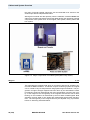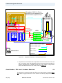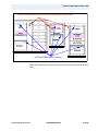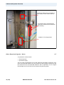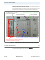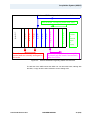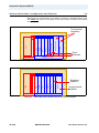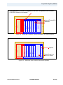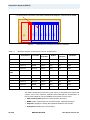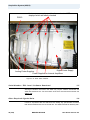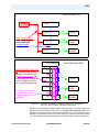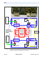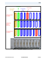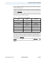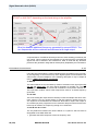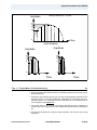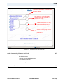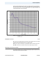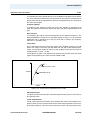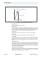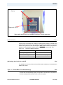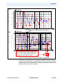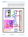
1
"RUKERå"IO3PIN
AVANCE III
NMR Hardware
User Guide
Version 001
THINKåFORWARDå
NMR Spectroscopy
The information in this manual may be altered without notice.
BRUKER BIOSPIN accepts no responsibility for actions taken
as a result of use of this manual. BRUKER BIOSPIN accepts
no liability for any mistakes contained in the manual, leading to
coincidental damage, whether during installation or operation of
the instrument. Unauthorized reproduction of manual contents,
without written permission from the publishers, or translation
into another language, either in full or in part, is forbidden.
This manual was written by
Eamonn Butler
Technical direction was provided by:
Dr. Frank Decker
This manual was edited and desktop published by:
Stanley J. Niles
© February 5, 2008: Bruker Biospin GmbH
Rheinstetten, Germany
P/N: Z31839
DWG-Nr.: Z4D10601 - 001
For further technical assistance on the AVANCE III unit, please
do not hesitate to contact your nearest BRUKER dealer or
contact us directly at:
BRUKER BioSpin GMBH
am Silberstreifen
D-76287 Rheinstetten
Germany
Phone:
FAX:
E-mail:
Internet:
+ 49 721 5161 0
+ 49 721 5171 01
[email protected]
www.bruker.com
Contents
Contents ............................................................... 3
1
1.1
1.2
1.3
1.4
1.5
1.6
2
2.1
2.2
2.3
2.4
2.5
2.6
2.7
2.8
2.9
3
3.1
3.2
3.3
3.4
User Guide Version 001
Introduction .......................................................... 11
Introduction ....................................................................... 11
Contact for Additional Technical Assistance ...................12
Systems to Which This Manual Applies .............................. 12
AVANCE vs. AVANCE II vs. AVANCE III ............................. 12
Units Specific to AVANCE Systems without SGUs ..........14
Units Specific to AVANCE Systems with SGUs ...............14
Additional Units Specific to AVANCE II Systems .............15
Additional Units Specific to AVANCE III Systems ............15
Units Common to all AVANCE Systems ..........................15
Format of Template Used in This Manual ........................... 15
Hardware in the Context of NMR ....................................... 16
Blanking and Gating Signals .............................................. 17
Cabinet and System Overview ............................ 19
Introduction ....................................................................... 19
Unit Location and Photograph ............................................ 21
General Information, Configuration and Function ............... 22
AQS Rack ......................................................................22
BSMS ............................................................................22
Amplifiers ......................................................................25
Magnet ..........................................................................26
Shim System .................................................................27
HPPR/Internal Preamplifiers ..........................................27
Lock System ..................................................................27
Probes ...........................................................................28
Overview of Principal Signal Paths .................................29
Switching the Unit On and Off ............................................ 29
Tips ‘n’ Tricks/Basic Troubleshooting ................................. 29
Serial Number / ECL Level / Software Download ................ 31
Other Required Signals / Units ........................................... 32
Option or Core Item ........................................................... 33
Further Information ............................................................ 33
Acquisition System (AQS/3) ................................ 35
Introduction ....................................................................... 35
Location and Photograph ................................................... 36
General Information, Configuration and Function ............... 38
Switching the Unit On and Off ........................................41
Safety Stop Indicator ..............................................42
Tips ‘n’ Tricks/Basic Troubleshooting ................................. 42
BRUKER BIOSPIN
3
Contents
3.5
3.6
3.7
3.8
4
4.1
4.2
4.3
4.4
4.5
4.6
4.7
4.8
4.9
5
5.1
5.2
5.3
5.4
5.5
5.6
5.7
5.8
5.9
4
Serial Number / ECL Level / Software Download ...............
Other Required Signals/Units ............................................
Option or Core Item ..........................................................
Further Information ...........................................................
44
44
45
45
IPSO ......................................................................47
Introduction ....................................................................... 47
Location and Photograph .................................................. 50
General Information, Configuration and Function ............... 50
Embedded PC ............................................................... 52
Tips ‘n’ Tricks/Basic Troubleshooting the Embedded PC 55
Other Required Signals / Units ...................................... 55
T –Controller ................................................................. 55
RCP outputs External IPSO. Connectors Z/A/B/C/D/E/F/G/
H/I 56
RCP Outputs AQS IPSO. Connectors Z/U/V/W .............. 57
RCP Output Specifications and Programming ................ 57
Tips ‘n’ Tricks/Basic Troubleshooting of the T-Controller 59
F –Controller ................................................................. 60
Tips ‘n’ Tricks/Basic Troubleshooting of F-Controllers .... 64
Specifications ................................................................ 64
G –Controller ................................................................. 64
Tips ‘n’ Tricks/Basic Troubleshooting the G-Controller ... 65
R–Controller .................................................................. 65
Troubleshooting the R-Controller ................................... 67
Overview of Slot Allocation ............................................ 68
Review .......................................................................... 68
Front Panel Connections: External IPSO ....................... 69
Front Panel Connections: AQS IPSO ............................. 71
Switching the Unit On and Off ........................................... 72
Tips ‘n’ Tricks/Basic Troubleshooting ................................. 73
Serial Number / ECL Level / Software Downloads .............. 75
Other Required Signals / Units .......................................... 76
Option or Core Item .......................................................... 76
Further Information ........................................................... 76
Signal Generation Unit (SGU/2) ...........................77
Introduction ....................................................................... 77
Location and Photograph .................................................. 82
General Information, Configuration and Function ............... 82
Front Panel Connections ............................................... 88
Specifications ................................................................ 90
Switching the Unit On and Off ........................................... 92
Tips ‘n’ Tricks/Basic Troubleshooting ................................. 93
SGU Unitool .................................................................. 94
Serial Number / ECL Level / Software Download ............... 96
Other Required Signals / Units .......................................... 96
Option or Core Item .......................................................... 96
Further Information ........................................................... 96
BRUKER BIOSPIN
User Guide Version 001
Contents
6
6.1
6.2
6.3
6.4
6.5
6.6
6.7
6.8
6.9
7
7.1
7.2
7.3
7.4
7.5
7.6
7.7
7.8
7.9
8
8.1
8.2
8.3
8.4
8.5
8.6
8.7
8.8
8.9
9
9.1
9.2
9.3
9.4
9.5
9.6
9.7
9.8
9.9
User Guide Version 001
ELCB .................................................................... 97
Introduction ....................................................................... 97
Location and Photograph ................................................... 97
General Information, Configuration and Function ............... 97
Front Panel Connections ................................................98
Specifications ................................................................98
Switching the Unit On and Off ............................................ 99
Tips ‘n’ Tricks/Basic Troubleshooting ............................... 100
Serial Number / ECL Level / Software Downloads ............ 100
Other Interacting Signals and Units .................................. 101
Option or Core Item ......................................................... 101
Further Information .......................................................... 102
GAB/2 ..................................................................103
Introduction ..................................................................... 103
Location and Photograph ................................................. 103
General Information, Configuration and Function ............. 103
Front Panel Connections .............................................. 104
Specifications .............................................................. 105
Switching the Unit On and Off .......................................... 106
Tips ‘n’ Tricks/Basic Troubleshooting ............................... 106
Serial Number / ECL Level / Software Downloads ............ 109
Other Interacting Signals and Units .................................. 110
Option or Core Item ......................................................... 110
Further Information .......................................................... 110
SCB20 ................................................................. 111
Introduction ..................................................................... 111
Location and Photograph ................................................. 111
General Information, Configuration and Function ............. 112
Front Panel Connections .............................................. 113
Specifications .............................................................. 113
Switching the Unit On and Off .......................................... 114
Tips ‘n’ Tricks/Basic Troubleshooting ............................... 114
Serial Number / ECL Level / Software Downloads ............ 114
Other Interacting Signals and Units .................................. 114
Option or Core Item ......................................................... 114
Further Information .......................................................... 114
1/4 Router ........................................................... 115
Introduction .....................................................................
Location and Photograph .................................................
General Information, Configuration and Function .............
Front Panel Connections .................................................
Switching the Unit On and Off ..........................................
Tips ‘n’ Tricks/Basic Troubleshooting ...............................
Serial Number / ECL Level / Software Download ..............
Other Required Signals / Units .........................................
Option or Core Item .........................................................
BRUKER BIOSPIN
115
116
119
120
120
121
121
121
121
5
Contents
10
10.1
10.2
10.3
10.4
10.5
10.6
10.7
10.8
10.9
11
11.1
11.2
11.3
11.4
11.5
11.6
11.7
11.8
11.9
12
12.1
12.2
12.3
12.4
12.5
12.6
12.7
6
External Amplifiers ............................................. 123
Introduction ..................................................................... 123
Location and Photograph ................................................ 125
General Information, Configuration and Function ............. 125
edsp/edasp Control ..................................................... 126
Mini-router and Combiners .......................................... 129
Amplifier Naming Convention ....................................... 131
Introduction to the Amplifier Service Web .................... 131
Proton Amplifier ........................................................... 133
BB Amplifier ................................................................ 134
BLAX500 ............................................................. 134
BLA2X500 ........................................................... 134
BLAX300 ............................................................. 134
Combined Proton and BB Amplifier .............................. 135
BLAXH 300/100 ................................................... 135
Combined Proton, Deuterium and BB Amplifier ............ 135
Front Panel ................................................................. 139
Characteristic of Good Amplifiers ................................. 142
Switching the Unit On and Off ......................................... 143
Tips ‘n’ Tricks/Basic Troubleshooting ............................... 143
Serial Number / ECL Level / Software Download ............. 143
Other Required Signals /units .......................................... 143
Option or Core Item ........................................................ 143
Further Information ......................................................... 144
Internal Amplifiers .............................................. 145
Introduction ..................................................................... 145
Location and Photograph ................................................ 146
General Information, Configuration and Function ............. 146
BLA2BB Front Panel ................................................... 149
BLAX300 Front Panel .................................................. 151
Switching the Unit On and Off ......................................... 151
Tips ‘n’ Tricks/Basic Troubleshooting ............................... 152
Serial Number / ECL Level / Software Download ............. 152
Other Required Signals / Units ........................................ 152
Option or Core Item ........................................................ 152
Further Information ......................................................... 152
Amplifier Specifications ............................................... 153
Internal Preamplifiers ......................................... 157
Introduction ..................................................................... 157
Location and Photograph ................................................ 158
General Information, Configuration and Function ............. 159
Front Panel Connections: 1H/2H Module ..................... 160
Front Panel Connections: X-BB Module ....................... 162
Specifications .............................................................. 162
Switching the Unit On and Off ......................................... 162
Tips ‘n’ Tricks/Basic Troubleshooting ............................... 162
Serial Number / ECL Level / Software Downloads ............ 162
Other Interacting Signals and Units ................................. 162
BRUKER BIOSPIN
User Guide Version 001
Contents
12.8
12.9
13
13.1
13.2
13.3
13.4
13.5
13.6
13.7
13.8
13.9
14
14.1
14.2
14.3
14.4
14.5
14.6
14.7
14.8
14.9
15
15.1
15.2
15.3
15.4
15.5
15.6
15.7
15.8
15.9
16
16.1
User Guide Version 001
Option or Core Item ......................................................... 163
Further Information .......................................................... 163
HPPR/2 ................................................................165
Introduction ..................................................................... 165
Location and Photograph ................................................. 165
General Information, Configuration and Function ............. 166
OBS Mode ................................................................... 166
Decouple Mode ............................................................ 168
Lock Mode ................................................................... 169
Tune Mode .................................................................. 169
HPPR/2 Cover Displays ............................................... 169
Specifications .............................................................. 171
Switching the Unit On and Off .......................................... 171
Tips ‘n’ Tricks/Basic Troubleshooting ............................... 171
Serial Number / ECL Level / Software Download .............. 172
Other Required Signals/Units ........................................... 172
Option or Core Item ......................................................... 172
Further Information .......................................................... 172
Receiver ..............................................................173
Introduction ..................................................................... 173
General Information, Configuration and Function ............. 174
Receiving Function ...................................................... 174
Digitizing Section ......................................................... 179
Anti-Aliasing Filters ...................................................... 180
Location and Photograph ................................................. 183
Front Panel RXAD-BB and RXAD ................................ 184
Switching the Unit On and Off .......................................... 185
Tips ‘n’ Tricks/Basic Troubleshooting ............................... 186
Serial Number / ECL Level / Software Download .............. 186
Other Required Signals / Units ......................................... 187
Option or Core Item ......................................................... 187
Further Information .......................................................... 187
DRU .....................................................................189
Introduction ..................................................................... 189
Location and Photograph ................................................. 190
General Information, Configuration and Function ............. 190
DRU and DRU-E Front Panel ....................................... 192
DRU Specifications .............................................. 193
Switching the Unit On and Off .......................................... 193
Tips ‘n’ Tricks/Basic Troubleshooting ............................... 193
Serial Number / ECL Level / Software Download .............. 196
Other Required Signals / Units ......................................... 196
Option or Core Item ......................................................... 196
Further Information .......................................................... 196
Reference Unit ....................................................197
Introduction ..................................................................... 197
BRUKER BIOSPIN
7
Contents
16.2
16.3
16.4
16.5
16.6
16.7
16.8
16.9
17
17.1
17.2
17.3
17.4
17.5
17.6
17.7
17.8
17.9
18
18.1
18.2
18.3
18.4
18.5
18.6
18.7
18.8
19
19.1
19.2
19.3
19.4
19.5
19.6
19.7
19.8
19.9
8
Location and Photograph ................................................ 198
General Information, Configuration and Function ............. 199
Specification ........................................................ 201
Front Panel ................................................................. 201
Switching the Unit On and Off ......................................... 202
Tips ‘n’ Tricks/Basic Troubleshooting ............................... 202
Serial Number / ECL Level / Software Download ............. 202
Other Required Signals / Units ........................................ 203
Option or Core Item ........................................................ 203
Further Information ......................................................... 203
PSD/3 Board ....................................................... 205
Introduction ..................................................................... 205
Location and Photograph ................................................ 205
General Information, Configuration and Function ............. 205
Front Panel Connections ............................................. 207
Specifications .............................................................. 207
Switching the Unit On and Off ......................................... 208
Tips ‘n’ Tricks/Basic Troubleshooting ............................... 208
Serial Number / ECL Level / Software Downloads ............ 208
Other Interacting Signals and Units ................................. 208
Option or Core Item ........................................................ 208
Further information .......................................................... 208
GREAT 1/10 and 3/10 .......................................... 209
Introduction ..................................................................... 209
Location and Photograph ................................................ 209
General Information, Configuration and Function ......... 211
Front Panel Connections: GREAT3/10 ......................... 211
Front Panel Connections: GREAT1/10 ......................... 212
Specifications .............................................................. 212
Switching the Unit On and Off ......................................... 213
Tips ‘n’ Tricks/Basic Troubleshooting ............................... 213
Serial Number / ECL Level / Software Downloads ............ 215
Other Interacting Signals and Units ................................. 215
Option or Core Item ........................................................ 215
Further Information ......................................................... 215
AQS 2H-TX .......................................................... 217
Introduction ..................................................................... 217
Location and Photograph ................................................ 217
General Information, Configuration and Function ............. 218
Front Panel Connections ............................................. 219
Specifications .............................................................. 220
Switching the Unit On and Off ......................................... 221
Tips ‘n’ Tricks/Basic Troubleshooting ............................... 221
Serial Number / ECL Level / Software Downloads ............ 221
Other Interacting Signals and Units ................................. 222
Option or Core Item ........................................................ 222
Further Information ......................................................... 222
BRUKER BIOSPIN
User Guide Version 001
Contents
Figures ............................................................... 223
Tables ................................................................. 227
Index .................................................................. 229
User Guide Version 001
BRUKER BIOSPIN
9
Contents
10
BRUKER BIOSPIN
User Guide Version 001
Introduction
1
Introduction
1
1.1
This manual is intended to serve as a single introductory hardware guide to
AVANCE III spectrometers. The AVANCE III series is characterized specifically by
the presence of an IPSO unit. At this stage it is sufficient to describe the IPSO (Intelligent Pulse Sequence Organizer) as a unit that controls the sequence and precise timing of all pulses which are timing-critical in terms of data acquisition. This
manual has been written primarily for operators who wish to have basic information regarding the system components and how they interact with one another. It
is not intended as a service guide and is not intended to equip the reader to carry
out any service or repairs. However there is an ever increasing desire for users to
understand the underlying hardware so they can
•
•
•
•
optimize their existing system’s performance
operate the system safely
choose the most appropriate system for their needs
make sensible decisions regarding expanding or upgrading current systems
At a more fundamental level there is a widely held belief that as spectrometers become more and more complex the operators have less and less of an understanding of the spectrometer hardware.This manual is intended to help reverse that
trend. It is also hoped that the reader will come to appreciate some of the design
issues involved in modern spectrometer systems.
Although the days when the spectrometer hardware could be described comprehensively in a single manual are long gone, this manual will attempt to provide the
reader with a concise overview of the main components of the system console.
Separate standalone systems such as the VTU and GREAT amplifiers, various
accessories such as MAS and Sample Changer as well as probes and magnets
are described in other manuals and this information will not be duplicated
here.This manual will attempt to explain principally the hardware housed inside
the cabinet. There is the danger that attempting to include too much information
will simply result in a manual that will gather dust on the shelf. The emphasis in
this manual is to provide as much information as possible without overloading the
reader with too many technical details. For this reason some of the explanations
and descriptions are deliberately presented in a simplified manner hopefully not at
the expense of strict technical and scientific correctness. It would also be impossible to provide any realistic comprehensive overview of what is a very extensive
system. Where adequate descriptions would be too lengthy or too complicated
these areas are simply not included. At the end of each chapter there is however
a section entitled ‘Further information’ should the reader require more details on
any particular item.In particular this section will include references to specific
manuals on the BASH CD.
This manual is intended to improve the reader’s understanding of the console
hardware and go someway towards making NMR more rewarding. This manual
will not teach you how to operate the system or run basic experiments. For this
User Guide Version 001
BRUKER BIOSPIN
11 (235)
Introduction
you are referred to the manual entitled AVANCE AV (SGU Based Frequency Generation) Beginners Guide P/N Z31633e.
With these reservations in mind it is hoped that the reader is sufficiently motivated
to read on! If you have any corrections or comments with regard to improving this
manual please refer to below.
Contact for Additional Technical Assistance
1.1.1
NMR service and support team
BRUKER BioSpin GMBH
am Silberstreifen
D-76287 Rheinstetten
Germany
Phone:
FAX:
E-mail:
Internet:
+ 49 721 5161 0
+ 49 721 5171 01
[email protected]
www.bruker-biospin.de
Systems to Which This Manual Applies
1.2
This manual is written primarily for the AVANCE III IPSO based spectrometer
range though some features are also relevant to earlier systems which were not
fitted with the IPSO unit. The preceding spectrometer range (AVANCE II) has
been described in a manual entitled NMR Hardware Guide (P/N Z31756) but bear
in mind that there is always some overlap between the different configurations.
The next few sections serves to differentiate between the various systems and
has been included particularly for those more experienced operators that have
worked on Bruker systems down through the years. If you are new to Bruker systems you might want to skip down to section 1.4.
AVANCE vs. AVANCE II vs. AVANCE III
1.3
New spectrometer hardware is constantly being updated and there is a wide
range of available spectrometer configurations. For the purposes of explaining the
different hardware generations it is usually helpful to group the various configurations into various categories as outlined in Table 1.1. below. As mentioned earlier
information on earlier systems has been included to ground experienced users.
For operators who have recently acquired an IPSO system then column four is
most relevant. The development of the IPSO system is by far the most significant
recent development and it is the presence of this unit that defines the AVANCE III
(column four).
Prior to that, the two most significant advances were the SGU followed by the
DRU. The presence or absence of these developments can be clearly seen to differentiate the various systems as outlined in Table 1.1.. In this respect column
one is differentiated from two and three on the basis of whether SGUs are fitted or
not. More recently a major advance was the new DRU which is also used in the
table as a distinguishing feature of the recent AVANCE II series outlined in column
three.
12 (235)
BRUKER BIOSPIN
User Guide Version 001
Introduction
In parallel with these ‘configuration defining’ advances there have been of course
many other developments. Among the more recent ones have been the development of
•
•
•
a BSMS/2 with several new boards
•
•
an expanded range of internal amplifiers
internal AQS preamplifiers
a REF unit that ensures synchronization of all timing critical signals throughout
the entire spectrometer
additional Ethernet capability to many units
While much of the details in the table below may appear daunting at this stage
(depending of course upon the reader’s experience) the information is presented
here so that the reader can gain an overview of the various configurations.
One of the difficulties of presenting a single manual to describe different configurations of spectrometer is that the reader can find it difficult to keep sight of their
particular system. For this reason Table 1.1. may also serve as a useful reference
as the reader proceeds through this manual.
Table 1.1.
AVANCE
(without
SGU)
Summary of Four Generations of Spectrometer Hardware
AVANCE
(with SGU)
AVANCE II
(with DRU)
AVANCE III
(with IPSO)
Comment
AQR/AQX
AQS
AQS or AQS/2
AQS/3
Some early AVANCE III systems
may have been fitted with an
AQS/2. Two configurations of
IPSO are available an AQS version and an external version.
TCU0 or
TCU1
TCU3
TCU3
T-Controller
Located within the IPSO unit.
The IPSO is the distinguishing
feature of the AVANCE III
FCU0
FCU3
FCU3 or FCU4
F-Controller
Located within the IPSO unit
n/a
n/a
n/a
R-Controller
(optional)
Located within the IPSO unit
CCU10 or
CCU11
CCU10 or
CCU11
CCU10 or
CCU11
IPSO Host
The combination of the host,
one T-Controller, one (optional)
R-Controller as well as a number of F-Controllers are the main
components of the IPSO unit.
ASU + LOT
+ PTS or
Schomandl
SGU
SGU
SGU/2
Historically the introduction of
SGUs was a most significant
development. The latest SGU/2
can deliver RF output at both the
RF OUT and AUX OUT connection.
User Guide Version 001
BRUKER BIOSPIN
13 (235)
Introduction
Table 1.1.
Summary of Four Generations of Spectrometer Hardware
AVANCE
(without
SGU)
AVANCE
(with SGU)
ROUTER 3/5
ROUTER 3/5
ROUTER 3/5
1/4 ROUTER
Many standard IPSO systems
require no ROUTER, such is the
improved switching capability of
the SGU/2.
External
amplifiers
only
External or
internal
amplifiers
External or
internal amplifiers
External or
internal amplifiers
Internal and external amplifiers
can not be mixed.
RX22
RX22 or
RXBB
RXAD
AQS/2 only.
RXAD or RXADBB
The BB version is used for solids.
SADC/
HADC/FADC
SADC/
HADC/FADC
RXAD
RXAD or RXADBB
The RXAD performs digitizer
function
RCU
RCU
DRU or DRU-E
DRU or DRU-E
The DRU is the distinguishing
feature of AVANCE II.
REF 22 or
REF
REF or REF /2
REF or REF /2
Earlier generation spectrometers had no direct equivalent of
the REF unit.
AVANCE II
(with DRU)
AVANCE III
(with IPSO)
Units Specific to AVANCE Systems without SGUs
Comment
1.3.1
AQX / AQR chassis
FCU0
TCU0 or TCU 1
ASU (Amplitude Setting Unit)
LOT (Local Oscillator Tune)
PTS or Schomandl frequency synthesizer.
Units Specific to AVANCE Systems with SGUs
1.3.2
AQS chassis
FCU3 / FCU4
TCU3
SGU
REF22
Amplifiers can be internal or external.
14 (235)
BRUKER BIOSPIN
User Guide Version 001
Introduction
Additional Units Specific to AVANCE II Systems
1.3.3
DRU
RXAD
AQS/2
REF or REF/2
Additional Units Specific to AVANCE III Systems
1.3.4
IPSO comprising of a host as well as one T-Controller, one (optional) R-Controller
as well as a number of F-Controllers.
SGU/2
External amplifiers and Gradient unit with Ethernet interface.
Units Common to all AVANCE Systems
1.3.5
ROUTER (different versions)
External amplifiers (different versions)
HPPR (different versions)
Format of Template Used in This Manual
1.4
With the exception of this introductory chapter each spectrometer unit has been
described using a set of standard headings listed below. With such a large range
of units this format has been used to help the operator locate the required information speedily and efficiently, even though no single template will suit all units.
When in the case of a specific system unit there is no relevant information then
this heading is either described as na (not applicable) or simply not included.The
headings used in the following chapters are:
•
Introduction: This will give an overview of the unit and an outline of the role it
plays in the overall spectrometer operation. This section often highlights differences to previous generations of the same or similar units.
•
Location and Photograph: For many operators physically recognizing and locating the various units is an important first step in coming to terms with the
hardware.
•
General Information, Configuration and Function: This is a self explanatory
heading. Included in this section will be specifications where applicable as well
as an explanation of some signals accessible at the front panel.
•
•
Switching the Unit On and Off.
User Guide Version 001
Tips ‘n’ Tricks/Basic Troubleshooting: Bear in mind that this is not a service
manual but many operators express an interest in learning about some rudimentary troubleshooting checks.
BRUKER BIOSPIN
15 (235)
Introduction
•
Serial Number / ECL Level / Software Download: In terms of communicating
with Bruker service personnel this information is often very relevant.
•
Other Required Signals/Units: One of the major issues with troubleshooting
modern spectrometers is clearly isolating and identifying the faulty unit if and
when a problem arises.
•
Option or Core Item: This section has been included to help operators understand the various configurations possible.
•
Further Information: This will usually be a BASH reference so that the reader
can research the unit further.
Hardware in the Context of NMR
1.5
To help put the following chapters into context it is perhaps useful to consider the
principal generic features that are required of modern NMR hardware. Much of
the system design is aimed at achieving some of the features listed below
The transmitted excitation signals should have
•
precisely defined pulse lengths with accurately regulated amplitudes, frequency and phase control as well as fast switching of same
•
good on/off ratios (maximum suppression of noise etc. outside of signal transmission)
•
•
•
•
steep falling and rising edges of rectangular pulses
shaped pulses with well defined envelopes
linear and accurate amplification
high resolution in terms of frequency, phase and amplitude.
The received NMR signal should
•
be amplified linearly over a large dynamic range and the receiver output
should be optimally matched to the ADC input
•
be digitized at a high sampling rate to maximize the available sweep width and
facilitate oversampling. (‘On the fly’ processing of digitized data to facilitate
decimation and digital filtering should also be possible).
•
have good resolution (high number of bits assigned to the amplitude of the digitized signal)
•
maintain phase coherence over repeated acquisitions.
There should also be complete synchronization between all units with respect to
timing and in particular between transmission and receiving. The switching time
between transmit and receive must also be optimized. The development of the
REF unit has ensured that all timing critical signals used throughout the spectrometer are sourced from one single crystal oscillator. Furthermore the design is such
that transmit and receive switching signals used at various locations are generated on the one unit (namely the OBS SGU). Finally, as will be discussed later, the
entire IPSO concept ensures that the sequencing of all timing critical events takes
places on one single individual electronic chip.
Keeping the above essential features in mind will help the reader understand the
various roles performed by many of the individual units described in the following
chapters.
16 (235)
BRUKER BIOSPIN
User Guide Version 001
Introduction
Blanking and Gating Signals
1.6
As the concept will arise in several subsequent chapters it is perhaps informative
to explain the role played by these signals at this introductory stage. To generate
an RF pulse of a specific duration a continuos RF signal is first generated and
subsequently transmitted through an electronic switch which regulates the transmission in that it has two modes, on or off. This on/off switching is referred to as
blanking or gating the RF signal. The switches are controlled by blanking or gating
signals which are digital (TTL level) operating on active low logic.When the signal
is high (5V approx.) the switch is open to prevent transmission, when it goes low
(0V approx) the switch is closed to allow transmission.
Important features of rectangular pulses are good on/off ratios as well steep falling
and rising edges as mentioned earlier. The on/off ratio can be improved by repeated blanking or gating. Clearly if the blanking/gating is to be repeated at several locations the various controlling signals must be accurately synchronized. The role
played by the REF unit along with the SGU in terms of synchronizing the blanking
has already been alluded to.
The trend in the latest spectrometer systems is to minimize the requirement for
blanking by only generating RF signal during those times when transmission is to
occur. Thus the SGU output is switched off outside of transmission (see Figure
1.1.). There is still a need for blanking within the amplifier itself as they will inevitably amplify noise at all times.
User Guide Version 001
BRUKER BIOSPIN
17 (235)
Introduction
Pulse train as
defined by
pulse program
SGU
generation
Digital blanking/gating
pulse applied
to amplifier
Amplified RF
signal
Blanking of amplifiers outside of transmission maximizes noise
suppression
Figure 1.1. Concept of Blanking/Gating in Terms of on/off Switching
18 (235)
BRUKER BIOSPIN
User Guide Version 001
Cabinet and System
Overview
2
Introduction
2
2.1
The purpose of the cabinet is to
•
•
•
house the various spectrometer units in a compact arrangement
provide shielding to sensitive electronic components
ease site planning, installation and provision of services.
Shielding of sensitive components such as the receiver from interference arising
from electromagnetic radiation from external sources is maximized when all the
units are housed within a metal cabinet.The reader should note that they are advised to keep the cabinet doors shut to maximize this shielding. Ventilation fans
mounted at the rear of the cabinet cool the various units. As well as providing important electrical internal wiring (via an internal wiring harness) the cabinet is designed to provide the spectrometer pneumatic and mains electrical power
connections. With a cabinet arrangement it is easier to provide facilities such as
electrical power and compressed air from a single supply.These connections can
be seen in Figure 2.1..
The cabinet can be moved relatively easily (power all units off and disconnect cabling if required) and its position, particularly with respect to the magnet, is an important site planning consideration. In many situations site planning is reduced to
providing suitable locations for the cabinet, the operator desk and the magnet.
From an operator/customer perspective the only other principal consideration is
whether they require a MicroBay, OneBay or TwoBay cabinet and this depends almost entirely on the configuration of the spectrometer (see below for further details).
User Guide Version 001
BRUKER BIOSPIN
19 (235)
Cabinet and System Overview
Pressure Adjust
Safety Fuses
Pneumatic Connections
Pressure Gauge
Figure 2.1. Rear View of Base of Cabinet.
20 (235)
BRUKER BIOSPIN
User Guide Version 001
Cabinet and System Overview
Unit Location and Photograph
2.2
Single Bay
A Q S 3
Micro Bay
E th . S W IT C H
IP S O
A Q S
IP S O
A Q S 3
E th . S W IT C H
B L A X H 2 H
B L A X 3 0 0
B S M S /2
B S M S /2
M A S
A Q S 3
B V T
IP S O
B L A ...
E th . S W IT C H
B L A ...
Two Bay
B L A ...
B L A ...
B S M S /2
Figure 2.2. Different Cabinet Configurations (not to scale)
User Guide Version 001
BRUKER BIOSPIN
21 (235)
Cabinet and System Overview
General Information, Configuration and Function
2.3
Whether the cabinet is MicroBay, OneBay or TwoBay will depend effectively on
the number of channels required.
•
•
A MicroBay cabinet will accommodate up to three independent RF channels.
•
A TwoBay cabinet will accommodate up to eight independent RF channels.
A OneBay cabinet will accommodate up to four independent RF channels (reduced to three if internal amplifiers are used).
Note that there is some scope to place some external units on top of the cabinet,
though be aware that such units do not benefit from the cabinet shielding.The
principal sub units housed within the cabinet are the AQS (Acquisition Control
System), the BSMS (Bruker Smart Magnet System), the VTU (Variable Temperature Unit) as well as various amplifiers (aka transmitters).These principal sub units
will now be discussed briefly in the context of a general introduction More details
will be provided subsequently.
AQS Rack
2.3.1
AVANCE III are now fitted with the AQS/3 as standard though the principal of operation is the same as with the previous AQS and AQS/2 racks. The various units
within the AQS prepare and in some cases amplify the radio frequency pulses
used to excite the sample and receive, amplify and digitize the NMR signals emitted by the sample. Once the data is received and digitized, the information is
transferred to the host computer for further processing and storage. The data
transfer is usually from the DRU (which acts as rack master) to the host computer
via the Ethernet switch. The AQS rack greatly reduces the space requirements of
the spectrometer. Several buses which run along the backplane make communication between the various units very efficient. Furthermore the combination of so
many units into a single rack greatly simplifies the provision of power supply voltages which are also delivered over the backplane to the various units. Depending
upon the configuration many of the AQS slots may be vacant but this is inevitable
when a single rack is used for multiple configurations.The AQS rack contains a
set of slot-in type units as well as the IPSO (where a 19” version is not used). A
more detailed description of the AQS is to be found in chapter 3.
BSMS
2.3.2
BSMS is an acronym for Bruker Smart Magnet control System. Depending upon
the configuration the system can be controlled via the
•
•
•
Commands entered directly from within the TOPSPIN BSMS display
BSMS shuttle
BSMS keyboard (optional extra only)
The principal functions of the BSMS are to
•
•
22 (235)
operate the lock system
control the shim system
BRUKER BIOSPIN
User Guide Version 001
Cabinet and System Overview
•
•
operate the sample lift and spin
generate gradient pulses (where a GAB/2 unit is fitted).
For an overview of some of the BSMS signals see "Simplified Schematic of
Principal Signal Paths" on page 30.The BSMS hardware is comprehensively
described in various manuals available on the BASH CD and will not be dealt with
in any great detail in this manual with the exception of some recently developed
boards such as the new
•
•
•
ELCB which will be described in chapter 6.
GAB/2 which will be described in chapter 7.
SCB20 which will be described in chapter 8.
A summary of the various boards follows and they will be discussed in the order in
which they are located (from the left) as in Figure 2.3.
Deuterium Amplifier 2H-Tx: This houses a single 20W amplifier primarily designed
to facilitate experiments that require deuterium decoupling.Note that there is also
an AQS version with 80W power which is enough to observe deuterium although
the 90 degree pulses are relatively long.There is also a BLAXH2H external amplifier which delivers 150W on the deuterium channel (up to 600 MHz systems) and
250W on the deuterium channel (700-900 MHz systems).The BSMS version mentioned above has limited power (20W) due to the current limit of the BSMS power
supplies.
Sample and Helium Level Control Board SLCB: This board is responsible for all
aspects of raising, lowering and spinning the sample as well as monitoring the Helium level. The pneumatic module which controls a supply of compressed air to
drive the lift and spin is located at the rear of the BSMS/2.
Gradient Amplifier Board GAB/2: This board receives digital data from the G-Controller and converts it into its analogue equivalent in order to perform Z axis gradient spectroscopy. For further details see chapter 7.
Shim Current Board SCB/20.This generates the shim currents for the room temperature shims based on the operator adjustments at the BSMS Keyboard, Shuttle or from within TOPSPIN. Effectively the board is a very sophisticated DAC with
high accuracy and resolution.Figure 2.3. shows a BSMS/2 with two of these
boards fitted. The actual number of boards fitted (one or two) will depend on the
complexity of the shim system. The font panel connections where the currents are
accessed are labelled in Figure 2.3.. From here the cabling ports the currents to
the rear of the cabinet and then on to the actual shim system located within the
magnet bore. The SCB20 will be dealt with in chapter 8.
Extended Lock Control Boards ELCB: This new board replaces the old LCB and
CPU. In its role as CPU it controls the BSMS and in particular the lock. The main
development has been the Ethernet capability. It also incorporates 2 TTY connectors for BACS, VTU, etc.For more details see chapter 6.
Lock Receiver Board LRX: Like the Transmitter this board is spectrometer frequency dependent and receives the NMR signal generated by the deuterated solvent. The signal is transmitted from the probe via the 2H module of the HPPR or
internal preamp.
Lock Transmitter Board LTX: This board generates the deuterium excitation signal required to maintain the lock and as such is spectrometer frequency dependent. Figure 2.3. shows a LTX600 signifying that is fitted on a 600 MHz
spectrometer. The signal generated by this board is transmitted to the 2H module
of the HPPR or internal preamplifier and then to the probe.
User Guide Version 001
BRUKER BIOSPIN
23 (235)
Cabinet and System Overview
Deuterium Amplifier
Extended Lock Control Board
Sample and Helium Level Control Boards
Lock Transmitter Board
Lock Receiver Board
Gradient Amplifier Board
Depending on the shim system one or two
Shim Control Boards may be fitted
Connections for room temperature shim currents
Figure 2.3. Front Panel of BSMS/2
VTU:
Depending on the model the Variable Temperature Unit may be a separate standalone unit or may be incorporated into the rear of the BSMS. The function of the
VTU is to control the sample temperature using a heater in conjunction with an air
or nitrogen gas transfer line. A thermocouple serves as a thermometer to constantly monitor the temperature in the vicinity of the sample. All these devices are
24 (235)
BRUKER BIOSPIN
User Guide Version 001
Cabinet and System Overview
attached to the base of the probe and are easily accessible.The VTU constantly
monitors the thermocouple reading and makes adjustments to the heater power to
maintain a regulated temperature. In terms of overall spectrometer hardware the
VTU is relatively simple and will not be dealt with in any detail in this manual.
However it is worth mentioning the ‘edte’ menu which contains the ‘self-tune’ tab.
Using the self-tune routine will optimize the temperature control parameters and
these results, which are probe specific, can then be stored on disk in files. In this
way it is relatively simple to load the appropriate set of parameters whenever a
probe is changed.
Figure 2.4. Typical VTU Unit (BVT3000)
Amplifiers
2.3.3
Also known as transmitters the amplifiers will be dealt with in detail in chapter 10
and chapter 11 but will be introduced here in the context of the overall hardware.
Signals of relatively large amplitude are often required to minimize the 90 degree
pulse lengths and optimally excite the NMR sample and hence the need for amplifiers. Amplifiers can be internal (incorporated into the AQS rack) or external (separate standalone units). One other option has been to incorporate a dedicated
deuterium amplifier into the BSMS/2 as described in section 2.3.2. Cables running
directly from the amplifier outputs to the hppr/internal preamplifiers carry the RF
signal to the sample. Although there is a wide range of available amplifiers (including amplifiers for solid state NMR) the two main categories are:
Selective amplifiers (also known as 1H or proton amplifiers) are specifically
designed to amplify the higher frequencies associated with 1H and 19F
spectroscopy.
Broadband amplifiers (also known as X amplifiers) designed to amplify a
wide range of lower frequencies (excluding 1H and 19F) but including
13C,31P etc.
A third minor category mentioned above are dedicated deuterium amplifiers.
The RF signal enters the amplifier via the SMA type connector usually labelled
“RF in” on the front panel (see Figure 10.8. for an example of different connector
types). This is a relatively weak signal with a maximum amplitude of 1Vpp. However the quality of this signal is critical as it defines the frequency, timing, shape
and phase of the final signal. Experienced operators sometimes view this signal
on an oscilloscope. The function of the amplifier is to take the input signal and apply a fixed gain. Amplitude control and specifically amplitude variation is implemented prior to the amplifier, via the parameters (pl0...pl31) for rectangular pulses
and (sp0....sp63) for shaped pulses. The RF signal leaving the amplifier can be of
User Guide Version 001
BRUKER BIOSPIN
25 (235)
Cabinet and System Overview
the order of several hundred volts and is not recommended to be viewed on the
oscilloscope without adequate attenuation.
Although this manual will deal primarily with the hardware contained within the
cabinet it is perhaps appropriate to describe (albeit briefly) the remaining principal
components of the system such as the magnet, shim system, HPPR, probes and
lock system.
Figure 2.5. Major Components of an NMR System (MIcro-Bay Shown)
Magnet
2.3.4
This generates the magnetic field which in conjunction with the RF excitation signal induces NMR transitions. To maintain a super-conducting system the magnet
core is cooled to very low temperatures using liquid nitrogen and helium. The progression to higher strength magnets has been driven by the associated increase
in sensitivity. Apart from field strength the main consideration in terms of the ‘quality’ of the magnet is the homogeneity of the magnetic field and this has a direct
bearing on the resolution as determined by the line width of NMR signals. Both
sensitivity and line width (or line shape) are fundamental spectrometer specifications. The homogeneity of the magnet field may be adjusted using a procedure
known as ‘shimming’ described below.
26 (235)
BRUKER BIOSPIN
User Guide Version 001
Cabinet and System Overview
Shim System
2.3.5
The room temperature shim system, mounted into the lower end of the magnet, is
a set of current carrying coils (known as shims) used to maximize field homogeneity by offsetting any existing inhomogeneities caused by the sample itself, the
probe etc. The currents in these room temperature shims (so called as they are
not cooled by being immersed in a bath of liquid helium) are controlled by the
BSMS and may be adjusted from the BSMS keyboard, BSMS shuttle or from within TOPSPIN to optimize the NMR signal. The process of adjusting the shim currents is called ‘shimming’ and has a major effect on signal resolution and
sensitivity. The ‘lock level’ is often used to monitor the progress of the shimming
operation.
HPPR/Internal Preamplifiers
2.3.6
Although the HPPR (High Performance Preamplifier) carries the transmitted signal to the sample it is primarily concerned with magnifying the relatively weak signals emitted from the sample. The HPPR is located at the base of the magnet to
amplify the NMR signal at the earliest possible opportunity and thus minimize
losses along the cable. Newer internal preamplifier modules are incorporated in
the AQS rack within the cabinet itself and can be seen in Figure 3.1. Once the
signal has been amplified within the HPPR any subsequent losses in cabling are
less critical. The HPPR also transmits and receives the deuterium (or fluorine)
lock signal and is used in the wobble routine. Up to 8 individual modules (excluding the cover module which is always present) may be configured in the newest
versions known as the HPPR/2. All these modules will automatically be displayed
in the edsp/edasp window. A very common configuration consisting of three individual modules, a proton, X-BB and 2H along with a cover module, is shown in
Figure 2.6. The 2H module is used to transmit and receive the lock signal. Much
of the HPPR technology is concerned with what is known as the Transmit / Receive switching. Effectively the signal going to the probe is transmitted without any
action apart from frequency filtering to minimize noise as well as an inevitable insertion loss of typically 1dB. Once this transmit signal has elapsed the signal path
within the HPPR is altered so as to amplify the received signal from the probe by
typically 30dB. The trick is to make this switch as fast as possible and suppress
leakage so that the tail of the transmitted signal does not swamp the start of the
received signal.The timing of this switching is controlled by the OBS SGU.
The HPPR hardware is described in detail in manuals available on the BASH CD
and will be dealt with briefly in chapter 13.
Lock System
2.3.7
The aim of the lock system is to ensure that the strength of the magnetic field surrounding the sample does not change during an experiment or that the effect of
any external disturbances is minimized. The operator must be confident that the
magnetic field strength is always maintained at precisely the same strength and
this is referred to as ‘locking’ onto the sample. The lock system is essentially a
separate spectrometer designed to observe deuterium. It should be mentioned
that the signals emitted by deuterium are normally far removed from frequencies
that are generally of interest in NMR experiments. However if the deuterium frequency is unsuitable then a fluorine (19F) lock may be used. Since it is by far the
User Guide Version 001
BRUKER BIOSPIN
27 (235)
Cabinet and System Overview
Cover Display
Cover Module
Individual
Modules
QNP Module
Figure 2.6. HPPR/2
most popular, only the deuterium lock will be dealt with here, but the reader
should note that the operating principles of the deuterium and the fluorine lock are
identical.
In AVANCE systems the BSMS provides the hardware required to implement the
lock and a separate deuterium module in the HPPR or internal preamplifier transmits and receives the lock signals. Some deuterium must of course be introduced
into samples that are under analysis. This can most easily be done by dissolving
the sample in a deuterated solvent.
The frequency of the signals emitted by deuterium for a particular size of magnet
is precisely known. Therefore if the magnetic field strength is correct then any
deuterium in the sample for a given type of spin should emit this exact frequency.
If the magnet strength varies then so also will the deuterium frequency. The lock
system uses a receiver (housed in the BSMS rack) to monitor this deuterium frequency and makes adjustments to the magnetic field strength accordingly.
Probes
2.3.8
The probe is designed to hold the sample, transmit radio frequency signals which
excite the sample and detect the emitted response. The transmission and reception is achieved by using specially designed RF coils.The probe is inserted into
the bottom of the magnet and sits inside the room temperature shims. Coaxial cables carry the excitation signals from the HPPR/internal preamplifier to the probe
and the NMR signal back from the sample to the HPPR/internal preamplifier. As
mentioned in section 2.3.6 the preamplifiers are needed to boost the NMR signals
which are typically very weak.
28 (235)
BRUKER BIOSPIN
User Guide Version 001
Cabinet and System Overview
Overview of Principal Signal Paths
2.3.9
To help the reader appreciate the overall spectrometer operation before progressing to a description of the individual spectrometer units, it is hopefully informative
to give a very brief summary of some of the principal signals in a standard acquisition as in Figure 2.7.. The reader should note that this is a relatively simple example and details will vary depending on the particular spectrometer configuration.In
particular the example shown uses the HPPR as opposed to internal preamplifiers
as well as an AQS IPSO as opposed to a 19” IPSO.
Transmission of excitation signals: The details of the excitation pulse are prepared and generated by F-Controllers within the IPSO, based on information entered by the operator and transmitted from the workstation via the Ethernet link.
This digital information is then transmitted to the SGUs via the LVDS link. After
generation on the SGU the analog RF signal (1Vpp max) is connected to an amplifier before transmission to the appropriate HPPR module.
Transmit / Receive switching. The HPPR filters and transmits the excitation signal to the probe and then filters and amplifies the NMR (received) signal. Note
that the same cable carries the transmitted signal to the sample as well as the relatively weak signals emitted from the sample.
Received NMR signal: The signal is detected and amplified by the RXAD where
it is also digitised.The digitized signal is passed to the DRU and finally to the NMR
workstation via the Ethernet switch. The acquired signal is then processed and
stored.
Lock Signal: The BSMS transmits and receives the Lock signal via the HPPR 2H
(or alternatively the 19F) module.
Shim Control: This is achieved using the BSMS.
Both the lock and the shims can be controlled using the BSMS Keyboard, Shuttle
or from within TOPSPIN which communicates with the ELCB of the BSMS/2.
Switching the Unit On and Off
2.4
The cabinet and all power supplies are controlled by a red/green switch on the
front (see Figure 2.8.). Note in the event of an emergency this switch is the quickest way of removing electrical power from the various spectrometer units.The red/
green switch will remove all power immediately whereas individual unit switches
on the AQS or BSMS are normally used to power off units within the rack. Standalone items such as the VTU or external amplifiers have separate power switches.
Tips ‘n’ Tricks/Basic Troubleshooting
•
User Guide Version 001
2.5
The cabinet should be left permanently closed when operating as this will maximize the shielding and reduce the effect of any electromagnetic disturbances
from outside. Care is taken in choosing the material from which the cabinet is
constructed to maximize radiation shielding. Keeping the cabinet closed will
also reduce any disturbances caused by temperature fluctuations. The cabinet
is designed to be sealed from electromagnetic interference (see Figure 2.9.) It
is worth noting that steady temperatures in the laboratory itself are always conducive to reliable NMR data.
BRUKER BIOSPIN
29 (235)
Cabinet and System Overview
Allocation of SGU1 to Proton
and SGU2 to X-frequency is for
demonstration purposes only
I
P
S
O
ROUTER(option)
SGU3
SGU4
SGU2
SGU1
REFERENCE
DRU
RXAD
3/4
LVDS
Received Signal
MAGNET
analog signal 1Vpp
Ethernet Switch
RF input
Proton Amplifier
Amplified RF
RF input
HPPR
Broadband Amplifier
BSMS
SCB20
E
L
C
B
SCB20
L
o
c
k
R
e
c.
Cover Module
L
o
c
k
T
r
a
n
s
1H
X-BB
2H
Proton / X-BB excitation signal
Received NMR signal
Lock signal
Workstation
Shim control
LVDS link
Figure 2.7. Simplified Schematic of Principal Signal Paths
•
If a problem is encountered with the pneumatic driven functions such as lift and
spin you should check that adequate pressure (see site planning guides for
specific requirements) is available at the rear of the cabinet. The pressure
gauge and adjustment knob are clearly visible in Figure 2.1..
Serial Number / ECL Level / Software Download
2.6
The location of the serial number and ECL level of the cabinet is shown Figure
2.9.. While the physical structure of the cabinets is relatively independent of any
30 (235)
BRUKER BIOSPIN
User Guide Version 001
Cabinet and System Overview
Cabinet main switch will kill all power including AQS and BSMS
AQS and BSMS main switches
Figure 2.8. Mains Power Switches
engineering changes the internal wiring harness does change with new developments.
User Guide Version 001
BRUKER BIOSPIN
31 (235)
Cabinet and System Overview
Inside the cabinet door are details of
part number, serial number ECL etc.
The cabinet doors are designed to
seal when closed so as to maximise
RF shielding
Details of TTY assignments
Figure 2.9. Cabinet Production Details
Other Required Signals / Units
2.7
To operate the cabinet needs
•
•
electrical power
pneumatic supply
The only other consideration here is that cabinet should always remain the minimum recommended distance from the magnet to avoid magnetic interference with
the electronics.The recommended distances will be dependent on the magnet
field strength and can be found in the relevant site planning guide.
32 (235)
BRUKER BIOSPIN
User Guide Version 001
Cabinet and System Overview
Option or Core Item
2.8
The cabinet be it MicroBay, OneBay or TwoBay is a core item. In particular it is fitted with an internal wiring harness which transmits a range of signals and interconnects many units.
Further Information
2.9
•
Site Planning guides available on the BASH CD are useful references particularly with respect to cabinet dimensions, suitable location, electrical and pneumatic requirements etc.
•
There are a series of manuals on the various BSMS units not all of which will
be described in this manual.For an overview of the various units check out the
introductory chapter of BSMS (User Manual) P/N Z31185.
•
For an introduction to and overview of temperature control see Variable Temperature Unit (VTU) (User Manual) P/N Z31482.There are also several individual manuals describing the various models.
User Guide Version 001
BRUKER BIOSPIN
33 (235)
Cabinet and System Overview
34 (235)
BRUKER BIOSPIN
User Guide Version 001
3
Acquisition System
(AQS/3)
3
Introduction
3.1
ROUTER1/4 (Optional)
SGU3
SGU4
SGU1
SGU2
REFERENCE
DRU
RXAD
IPSO
The AQS/3 (Acquisition System) rack
greatly reduces the space requirements and simplifies the configuration
and operation of the spectrometer.
Several buses which run along the
backplane make communication between the various units very efficient.
Furthermore the combination of so
many units into a single rack greatly
simplifies the provision of power supply voltages which are again delivered over
the backplane to the various units.This minimizes the number of front panel cables. While the rack system offers a great space saving the large number of signals that are transmitted over the backplane are inaccessible making
troubleshooting in the field very challenging. The rack design is to allow for system flexibility in terms of unit configuration so that standard racks can be used for
various spectrometer configurations. The design of the AQS/3 has also had to
take account of the fact that it must be compatible with various units that have
been developed over time. These units have different physical sizes and use different communication protocols.
Since a single rack must often accommodate a range of configurations, both basic
and advanced, it is often the case that many of the slots will be unoccupied for any
particular configuration.This is particularly the case when the external IPSO unit is
fitted. A second rack can be added to allow a flexible extension for multi-receiving
systems.Every slot on the AQS/3 User Bus backplane is hardware coded, so that
every unit can be addressed individually via its unique slot address. So also can
each individual rack be distinguished from each other using a rack code which
can be set with rotary switches on the rear side of the AQS/3 backplane.
At this stage three versions of the AQS have been produced (original AQS, AQS/
2 and AQS/3). Although some early systems were fitted with the AQS/2 all
AVANCE III systems are now fitted with the AQS/3 and for the purposes of this
manual no other rack will be described.
The newest AQS/3 can accommodate the internal IPSO unit as well as having 10
slots for AQS type units.
When combined with an external IPSO the AQS will cater for
6 RF channels (system with external amplifiers)
3 RF channels (system with internal amplifiers)
A second AQS/3 will enable up to 8 RF channels to be installed.
User Guide Version 001
BRUKER BIOSPIN
35 (235)
Acquisition System (AQS/3)
When a AQS IPSO is fitted, the system will cater for 4 RF channels though this is
a limitation of the IPSO unit and not the AQS rack.
In the descriptions throughout this manual the term AQS should be read to mean
the AQS/3. Where a distinction is to be made this will be specifically stated.
Position and number of any unoccupied
slots will depend on the configuration
Unoccupied slot(s) to the right
of the IPSO is standard.
Internal Preamplifers
Internal Amplifier
DRU
SGU
SGU
RXAD
REF
AQS IPSO
Number of SGUs is dependent on number of channels
These three boards are always present and
are normally arranged in this order
Figure 3.1. Typical AQS/3 rack with AQS IPSO internal preamplifiers and amplifier.
Location and Photograph
3.2
The AQS is located inside the main cabinet (see Figure 2.2.)
36 (235)
BRUKER BIOSPIN
User Guide Version 001
Acquisition System (AQS/3)
Number of SGUs dependent on number of channels
Internal amps, occupying three slots each
I
P
S
O
D
R
U
R
X
A
D
R
E
F
S
G
U
S
G
U
These three boards are always
present and are normally arranged in
this order
S
G
U
P
R
E
A
M
P
R
O
U
T
E
R
Last slot:
Router
or
Internal
amps
or
Empty
Internal preamps, deuterium amplifier
if present will be located immediately
after the SGUs
Figure 3.2. General Guidelines Regarding AQS/3 Slot Allocation
The left end of the AQS houses the IPSO unit. All other AQS units, starting with
the DRU, occupy what are often referred to as the analog slots.
User Guide Version 001
BRUKER BIOSPIN
37 (235)
Acquisition System (AQS/3)
General Information, Configuration and Function
3.3
Although many configurations are possible a selection is illustrated below along
with Table 3.1. which is a summary of the max number of channels for various
configurations.
BLA2BB
BLAX300 (option)
SGU3 (option)
SGU2
SGU1
REF
RXAD
DRU
IPSO
Two Internal
Amplifiers
Three
Channels
IPSO Section
Analog Section
Figure 3.3. AQS/3 with Three Channels and Internal Amplifiers
IPSO Section
BLAXH
2HTX
SGU3
SGU2
SGU1
REF
RXAD
DRU
IPSO
Deuterium
Amplifier
Single Internal
Amplifier
Analog Section
Figure 3.4. AQS/3 with Three Channels 2H-TX and Internal Amplifier
38 (235)
BRUKER BIOSPIN
User Guide Version 001
Acquisition System (AQS/3)
BLA2BB
XBB PREAMP
1H/2H PREAMP
SGU2
SGU1
REF
Internal Preamplifier
Modules
RXAD
IPSO
DRU with preamp controller
The preamplifier controller is integrated in the DRU. A separate AQS PREAMP
CONTROL board is not needed
Analog Section
IPSO Section
Figure 3.5. AQS/3 with 2 Channels, Internal Preamplifiers and Internal Amplifier
IPSO Section
ROUTER 1/4
SGU3 (option)
SGU2
SGU1
REF
RXAD
DRU
IPSO
Optional
Space for up to a
total of 6 SGUs.
Analog Section
Figure 3.6. AQS/3 with Three Channels and External Amplifiers
User Guide Version 001
BRUKER BIOSPIN
39 (235)
Acquisition System (AQS/3)
IPSO Section
1/4 ROUTER
SGU6
SGU5
SGU4
SGU3
SGU2
SGU1
REF
RXAD
IPSO
DRU
For more than 4 SGUs in one rack a Reference Board/2 1000 must be used
Analog Section
Figure 3.7. AQS/3 with Six Channels and External Amplifiers
Table 3.1.
Maximum Number of Channels for Various Configurations
Transmitters
AQS IPSO
External
IPSO
Preamps
Optional
ROUTER
AQS/3
Max
channels
Limitation
internal
HPPR
no
one
3
Transmitters
internal
internal
no
one
2
AQS
external
HPPR
yes/no
one
4/4
IPSO
external
internal
yes/no
one
4/4
IPSO
internal
HPPR
no
one
3
Transmitters
internal
internal
no
one
2
AQS
external
HPPR
yes/no
one
6/7
AQS
external
internal
yes/no
one
4/5
AQS
external
HPPR
yes/no
two
8/8
IPSO
external
internal
yes/no
two
8/8
IPSO
The AQS is designed to house slot-in type units in an integrated rack system and
contains much of the electronic hardware associated with the spectrometer. In
fact it is often helpful to view an AVANCE spectrometer in terms of the:
•
•
•
•
40 (235)
AQS including IPSO (performs most acquisition functions)
BSMS system (controls the lock and shim system, sample lift and spin)
Amplifiers (amplify the analog RF signals transmitted to the sample)
Preamplifiers amplify the received signal
BRUKER BIOSPIN
User Guide Version 001
Acquisition System (AQS/3)
•
VTU: (controls the sample temperature).
The IPSO and various units of the AQS prepare the signal to be transmitted and
also receive, amplify and digitize the NMR signal emitted from the sample. Thus in
the AQS will be found:
•
•
•
•
•
•
One DRU, RXAD and REF unit
A number of SGU/2s
One Router (optional)
One deuterium amplifier (optional)
Internal amplifiers (in the case where there are no external amplifiers)
Internal preamplifiers (in the case where there is no external HPPR)
Apart from physically housing these units the rear of the AQS rack also provides
power supplies to the various units as well as electronic communication channels
(aka buses). Once the NMR data is received and digitized, the information is
transferred to the host computer for further processing and storage via the Ethernet link from the DRU. For more general communication the principal link with the
host computer is via the Ethernet link from the IPSO itself. It is important to emphasize that the Acquisition System has total control over spectrometer operation
within the duration of an experiment. This is to ensure uninterrupted operation and
so guarantee the integrity of the acquisition.
The analog section of the AQS/3 has nominally 10 rear connectors to the backplane though the number of units that can be installed will depend on their physical width. The backplane connector pin assignment is identical for all ten slots.
which means each common signal is accessible on every slot.The DRU acts as
rack master to ensure that the transfer of signals and data along the common
backplane is coordinated. (Exceptions to the identical pin assignment are the
power supply to the internal amplifiers and the data transfer to the DRU via
LVDS). Special connectors for the internal amplifiers can be clearly seen in Figure 3.9. As a result of this identical pin assignment there are various configurations possible depending on the number of racks, whether internal or external
amplifiers and preamplifiers are used, whether a ROUTER or internal deuterium
amplifier is fitted etc. As a general rule starting from the left the unit order is: DRU,
RXAD, REF, bank of SGUs, Internal preamplifiers, internal amplifiers or ROUTER(s) (see Figure 3.2.). Although some of these slot positions are interchangeable it has been decided to follow the general rule as stated above in all
installations.
A typical uxnmr.info display is shown in Figure 3.8. Starting from slot 0 the RXAD,
REF, a bank of SGU/2s and a ROUTER are clearly displayed.Note that the DRU
which is master of the AQS is listed separately above the other units.
The rear of the rack is primarily designed for power supplies, both digital, analog
and specialized power units for internal amplifiers.The rear also houses the PSD3
(Power Supply Distribution) unit.
Switching the Unit On and Off
3.3.1
The AQS is normally left switched on permanently. Integrated fans ensure that the
various units are constantly cooled. The on/off switch is located at the upper front
User Guide Version 001
BRUKER BIOSPIN
41 (235)
Acquisition System (AQS/3)
Figure 3.8. Extract from uxnmr.info file
left corner of the rack see Figure 3.9.. None of the individual units have separate
on/off switches and will automatically be switched on or off by the AQS mains.
In the event of an AC power loss to the spectrometer cabinet, the rack turns itself
off and restarts automatically when the power is restored. To prevent a short time
power outage an external UPS (uninterruptable power supply) must be fitted as
extra.
Safety Stop Indicator
The temperature inside the AQS rack is constantly monitored. Should this temperature exceed the set limit then as a safety precaution the power supply to the rack
will be shut off (without warning) and the Safety Stop indicator will light. The operator should establish the cause of the overheating before resetting the switch. A
reset can be done by switching the mains off and on. Possible sources of overheating are
•
•
failure of the cooling fans
too high an ambient room temperature or lack of sufficient air supply to the
fans.
The operation of all fans is individually controlled by the AQS controller (the DRU)
and the fan status can be checked on the chassis page in the DRU service web
(see Figure 3.11.).
Tips ‘n’ Tricks/Basic Troubleshooting
3.4
The AQS is not suitable for service in the field. Individual units should be removed
or swapped by service personnel only. While it is possible to view some front panel signals on an oscilloscope there is little scope for any troubleshooting, particu-
42 (235)
BRUKER BIOSPIN
User Guide Version 001
Acquisition System (AQS/3)
Main On/OFF Switch
Safety Stop Indicator
Part Number, ECL,
Serial Number, etc.
10 slots
Heavy duty connectors for internal amplifiers
Figure 3.9. AQS/3 Rack. Front View with all Boards Removed
larly with respect to the range of digital signals that use the AQS backplane. In
case of error
•
Check that the uxnmr.info entries (see Figure 3.8.) correspond to the specific
spectrometer configuration.
•
•
•
Check that cables on the front panels have not become loose or removed.
•
The length of external cable connections between the various units which carry
analog signals are usually kept as short as possible to minimize interference. If
a cable is to be replaced it is important to replace it with one of the same length
to ensure that no additional phase shifts are introduced.
•
As the DRU is the rack master the DRU Service Web is used to access the
AQS/3.
User Guide Version 001
Check that ‘power on’ indicator LEDs on the various front panels are lit.
If power LEDs on the various front panels are not lit then the LEDs on the power supplies at the rear of the AQS (see Figure 3.10.)should also be checked.
BRUKER BIOSPIN
43 (235)
Acquisition System (AQS/3)
Various power supply modules have extensive LED
displays which are easily checked
PSD/3
Digital Power Supply
Analog Power Supplies
Power Supplies for Internal Amplifiers
Figure 3.10. Rear View of AQS3
Serial Number / ECL Level / Software Download
3.5
Although individual units within the AQS may require software downloads the
AQS rack itself does not. For the location of the ECL level and serial number see
Figure 3.9..
Other Required Signals/Units
3.6
If there is a problem with the AQS there are hardly any spectrometer functions
that will be unaffected such is its central role. The AQS rack itself is relatively stan-
44 (235)
BRUKER BIOSPIN
User Guide Version 001
Acquisition System (AQS/3)
Figure 3.11. Extract from DRU Service Web: AQS Chassis Diagnostic Showing all 8 Fans Running
dalone though the Ethernet connections between the DRU and IPSO to the host
workstation must be working for the system to boot.
Option or Core Item
3.7
Every system will be fitted with one rack.There is the option to have more than
one rack fitted for multi-receiving systems. Each rack will then have its own DRU
as master.
Further Information
3.8
For information on the AQS/3 see the manual entitled AQS for IPSO systems
(TM) P/N Z31717. Readers should note that this manual also describes some of
the newer AQS individual units including the RXAD (Chapter 6) as well as the
DRU (Chapter 7).
User Guide Version 001
BRUKER BIOSPIN
45 (235)
Acquisition System (AQS/3)
46 (235)
BRUKER BIOSPIN
User Guide Version 001
IPSO
4
4
ROUTER1/4 (Optional)
SGU4
SGU3
SGU1
SGU2
REFERENCE
DRU
Precise timing control has always
been a critical feature of NMR spectroscopy, not only in terms of the excitation of the sample but also the
receiving of the emitted signals. Here
are just a few very simple examples to
illustrate where timing control is critical:
RXAD
4.1
IPSO
Introduction
•
Consider the critical timing in terms
of switching off the excitation signal
and opening the receiver. If the receiver is opened too early then it may be swamped by the excitation signal.
However if it is not opened early enough then sensitivity will be lost.
•
Modern excitation sequences involve complicated sequences on multiple
channels which must be implemented accurately wrt timing as well as frequency, phase and amplitude. Furthermore the various RF channels must be able
to operate independently as well as remaining synchronized with each other.
•
Repeatability of experiments can only be guaranteed if timing is accurately
controlled and reproducible.
•
Digitalization of the received analog signal is carried out in terms of a sample
and hold operation whose timing is always at the maximum allowed rate (regardless of the sweep width.) With the advances in oversampling, ‘on the fly’
processing and digital filtering, the timing is even more critical.
The ability to make meaningful real-time decisions on the basis of acquired data
processed on the fly can only be supported when the timing control is not only accurate but also can be adjusted almost instantaneously.
All of the above place increasing demands on the processing power capability of
the spectrometer.
To improve timing control as well as processing capability, the design philosophy
of the IPSO spectrometers has been to implement the control of all timing-critical
pulses on a single chip, often referred to as the sequencer. This sequencer lies at
the heart of the IPSO in that each IPSO board has immediate access to this chip.
(The R-Controller does not normally use the sequencer though it does have access to it.) Furthermore processing capability is enhanced because the implementation of the pulse sequences is much more efficient using the new simplified
architecture.
The IPSO (Intelligent Pulse Sequence Organizer) unit is a very significant development and is effectively the most distinguishing feature of the newest
AVANCE III spectrometer range. The IPSO has replaced almost all digital boards
User Guide Version 001
BRUKER BIOSPIN
47 (235)
IPSO
AQS IPSO
Digital Section
BLA2BB
XBB PREAMP
1H/2H PREAMP
SGU2
SGU1 MASTER
REF /2
RXAD
DRU
CCU
TCU3
FCU
FCU3/4
FCU
GCU
PREAMP CONRTOL
Almost the entire digital section has been replaced by IPSO.
Analog Section
TCU replaced with T-Controller
FCU replaced with F-Controller
GCU replaced with G-Controller
CCU replaced with Embedded PC
External IPSO
Figure 4.1. Schematic Displaying the Equivalency of Boards in the IPSO to
the Previous AQS Generation Boards (not to scale).
in the AQS (see Figure 4.1..) The CCU, TCU, FCU, GCU found in the previous
generation of spectrometer have been replaced by a single IPSO unit (albeit in
two possible configurations). Although this has obvious benefits in terms of space,
as well as cost savings due to uniformity of production, the principal driver has
been improved performance. In particular the timing control which was previously
carried out principally by the TCU has been improved (details later). Furthermore
as customer requirements increase, in terms of evermore exotic pulse sequences, the additional processing power delivered by the IPSO is a significant improvement.
A key aspect of timing control in AVANCE spectrometers is to ensure that up to
eight independent RF channels are precisely synchronized. In its simplest form
timing control reduces to ensuring that a series of pulses of precise duration is
generated in the correct order and delivered to the appropriate destination at the
right time.This is often referred to as sequencing. Clearly the correct sequencing
of these pulses is critical so that each channel and each unit remain precisely synchronized. Previously this was achieved by assigning timing control to the TCU
which was then used to control separate units such as the FCU and GCU. However no matter how well the various units were synchronized there is always the
48 (235)
BRUKER BIOSPIN
User Guide Version 001
IPSO
AVANCE II with TCU
TCU
DRU
20MHz
Real Time AQ Bus
Individual units synchronized with
common clock
FCU
LVDS
FCU
LVDS
SGU
LVDS
GCU
GREAT
R-Controller
IMPROVED Real Time AQ
Bus achieved by implementing all sequencing
on one physical chip. Individual units effectively become a single chip wrt
timing and sequencing.
AVANCE III with IPSO
T-Controller
20MHz
F-Controller
F-Controller
All timing critical signals
are controlled by a single piece of silicon, the
Sequencer.
SGU
G-Controller
LVDS
LVDS
SGU
SGU
LVDS
GREAT
Figure 4.2. Simplified Schematic Comparing Architecture of AVANCE II
with TCU and the Newer AVANCE III with IPSO
possibility of drift (however small) between individual units. The IPSO design has
enabled all the sequencing to take place on a single semiconductor chip. This
effectively ensures even more precise timing control since the possibility of drift
between two separate units has now been replaced by the much smaller possibility of drift between two different locations on the same chip. To put the timing con-
User Guide Version 001
BRUKER BIOSPIN
49 (235)
IPSO
trol into context, the reader should bear in mind that the shortest timing durations
possible are now 25ns and so we are in the realm of trying to eliminate incredibly
small variations. As mentioned earlier the processing requirements to generate
any particular sequence has been reduced with the simplified architecture resulting in enhanced performance in terms of capability and speed. Whereas previously the TCU had to effectively share its processing capability among the various
channels, the new simplified architecture means that each channel has dedicated
processing space on the chip and the various sequences are enacted with equal
efficiency irrespective of whether only one or all eight channels are active at any
given moment in time. Put most simply the new IPSO is faster, more precise and
has greater capability than previous generations. Figure 4.2. is an attempt to represent these concepts and in particular the new simplified architecture. Finally
even at this introductory stage it is worth emphasizing another aspect of the new
approach, namely that the same individual IPSO hardware board can be configured to perform different tasks. Previously there were several different hardware
units (TCU,FCU,GCU etc.) each designed specifically to perform specialized
functions.The IPSO approach uses application software to utilise the same hardware board for different tasks. As shown in Figure 4.3., depending on the application software, the same hardware board (the Tx-controller) can acts as either a TController, an F-Controller or a G-Controller. This has obvious benefits in terms of
unit cost production as well as flexibility in terms of spectrometer configuration.
There are three principal types of boards in the IPSO (see Figure 4.3.).
•
One Embedded PC which takes care of general (non timing-critical) communication.
•
A number of Tx–Controllers. Each Tx–Controller is physically identical. The
same hardware is configured to perform different functions as described
above.
A Tx–Controller configured to provide RCP outputs is referred to as a T-Controller
A Tx–Controller configured to control an SGU is referred to as an F-Controller
A Tx–Controller configured to control a gradient amplifier is referred to as a GController
•
One (optional) R-Controller which receives data from the DRU.
Note that the R-Controller, though not identical, is very similar to a Tx–Controller
with the LVDS transmitter replaced by an LVDS receiver
Location and Photograph
4.2
The IPSO has two configurations.
The AQS IPSO occupies the left hand (digital) section of the AQS/3 as in Figure
3.1..
The external IPSO is located beneath the AQS as in Figure 2.2..
General Information, Configuration and Function
4.3
The next section will discuss the various boards within the IPSO unit. As you read
this It may help the reader to refer to Table 4.1. which is a summary of the various
50 (235)
BRUKER BIOSPIN
User Guide Version 001
IPSO
The R Controller has an LVDS input
IPSO
LVDS
LVDS
Receiver
R-Controller
RCP
Outputs
LVDS
Transmitter
T-Controller
DRU-E
20Mhz
LVDS
LVDS
Transmitter
F-Controller
SGU
Embedded
PC
F-Controller
G-Controller
PCI Bus
LVDS
Transmitter
LVDS
LVDS
Transmitter
LVDS
SGU
GREAT
GAB/2
Sequencer
Ethernet Switch
These four boards are identical wrt hardware.
They are all Tx–Controllers with an LVDS output.
Application software is used to enable identical
hardware perform different functions.
Figure 4.3. Overview of Principal IPSO Units.
boards.The boards to be discussed will be the Embedded PC, T-Controller, FController, G-Controller and R-Controller.
Table 4.1.
Summary of IPSO Boards
Board
Number
Board Type
Replaces
Principal function
Embedded PC
One per system
Unique
CCU
General communication
T-Controller
One per system
Tx-Controller
TCU
Generates RCP outputs
F-Controller
One per SGU/2
Tx-Controller
FCU
Controls SGU
G-Controller
One per gradient unit
Tx-Controller
GCU
Controls gradient unit
R-Controller
One per system.
Optional extra
Unique (Modified
Tx-Controller)
User Guide Version 001
BRUKER BIOSPIN
Facilitates real time ‘on the fly’
processing of acquired data.
51 (235)
IPSO
Embedded PC
4.3.1
The function of the Embedded (IBM compatible) PC is to provide general communication between the various IPSO units as well as with the host workstation (via
the Ethernet switch). Communication internal to the IPSO is achieved over a standard PCI bus which is used for non timing-critical signals. (The Embedded PC
has no connection with the sequencer).
Figure 4.4. Internal View of 19’’ IPSO (left) and AQS IPSO (right). The Embedded PCs
are clearly marked
The Embedded PC is used to transfer information that is required prior to the
start of the acquisition via the PCI bus. Once an acquisition has started however, the sequencer bus would be used for timing-critical data. As an example, timing-critical data on the transmission side, such as the transfer of sequences in
real-time from the F-Controller to the SGU via the LVDS is still controlled ultimately by the Sequencer. On the receiving side timing critical operations such as ‘on
the fly’ processing of acquired data is controlled by the R-Controller or DRU.
Typical functions of the Embedded PC are:
52 (235)
•
Internal communication with the various IPSO boards via the standard PCI
bus.This link is shown in yellow in Figure 4.5. One typical example would be to
establish the type and number of IPSO boards installed using the ‘cf’ routine.
Note also that this bus is also used to configure each board as either a T, F, G
or R controller upon initial spectrometer startup.
•
External communication via the Ethernet link to the workstation. This link is effectively the means by which the commands entered at the operator desk are
transmitted to the IPSO. All acquisition parameters as well as pulse program
information are transmitted via the Ethernet link to the Embedded PC and then
to the DSP chip on the various controllers via the PCI bus. The physical link is
achieved by means of the Ethernet cable entering the IPSO front panel from
the Ethernet switch.
•
Control of 2 x RS232 links. These two links are labelled tty00 and tty01on the
front panel. tty00 is a dedicated link to the NMR workstation and tty01 is used
to communicate with external units such as the temperature unit (VTU), pneumatic unit etc. This enables these units to be operated from the operator desk.
BRUKER BIOSPIN
User Guide Version 001
IPSO
•
•
User Guide Version 001
Control of 2 x USB links. These are typically unused in current configurations.
Control of 2 x PCI slots.To physically increase the space use can be made of
an RS232 extension unit for controlling additional external units. Alternatively
the PCI slot can house a DPP unit which is used to calculate the digital pre emphasis for either a GREAT (gradient amplifier) or a GAB/2
BRUKER BIOSPIN
53 (235)
IPSO
.
S
G
U
/2
F-Controller
LVDS Transmitter
DSP
FIFO
Sequencer Bus
Channel 1
Front panel
LVDS connection to SGU/2 or
GREAT.
PCI Bus
Channel 2
Channel 3
Channel 4
Channel 5
Embedded
PC
Channel 6
FPGA
G
A
B
2
Channel 7
PCI Bus
Channel 8
Sequencer Bus
FIFO
LVDS Link
LVDS Transmitter
DSP
G-Controller
Figure 4.5. Schematic of principal IPSO board signal paths showing two channels in detail. Top
shows photo of board to same scale as schematic. Note that the entire timing control or 8
channels is achieved on the FPGA which is a single chip.
54 (235)
BRUKER BIOSPIN
User Guide Version 001
IPSO
The Embedded PC performs no on-board data manipulation processing or computation. Although it has an Ethernet link to the NMR workstation it is bypassed
when acquisition data is to be transmitted to the workstation. This data is transferred directly from the DRU via its own dedicated Ethernet link.
The Embedded PC boots from the TOPSPIN–PC via the Ethernet link. Powering
on or resetting the IPSO will automatically cause it to boot. In terms of equivalent
units in earlier generation spectrometers the Embedded PC is most like the CCU.
Tips ‘n’ Tricks/Basic Troubleshooting the Embedded PC
4.3.2
If the Embedded PC hangs then it may be necessary to initiate a reset. A reset
can be effected in several ways. Hardware resets can be implemented
1. by pressing the red (on/off) button on the front panel
2. by hitting the reset button on the front panel
Software resets can be implemented by
1. activating Linux commands such as ‘power off’, ‘reboot’ and ‘halt’ from within a
kermit shell
2. rebooting from within the IPSO service web page
The re-booting after a reset can be most easily observed by clicking on the Hyperterminal icon (Windows systems) or use the ‘CU’ command (Linux systems). Note
that the re-booting can only be observed if the tty00 connection is present.
Other Required Signals / Units
4.3.3
The Embedded PC plays such an important role in spectrometer operation that
should it fail most other functions will crash.
The unit itself requires power from the internal IPSO power supply as well as a
functioning Ethernet link to the host workstation in order to boot.
T –Controller
4.3.4
A T-Controller (Timing Controller) is effectively a Tx-Controller with specific application software.
•
•
There is one and only one T-Controller in each IPSO spectrometer.
•
The board position (see Figure 4.9.) is fixed regardless of the individual spectrometer configuration, number of channels etc. Indeed it is the board position
that designates a Tx-Controller as a T-Controller.
•
There is no distinction in hardware between the T-Controller board of a AQS
IPSO and the T-Controller board of an external IPSO
A single T-Controller is designed to provide the required signals for a spectrometer with up to 7 RF channels. (assuming an R-Controller is fitted)
Put most simply the T-Controller delivers a series of synchronous timing pulse sequences with very high resolution and accuracy which are used throughout the
spectrometer to control various functions and a wide range of units. These signal
User Guide Version 001
BRUKER BIOSPIN
55 (235)
IPSO
are referred to as RCP (Real-time Clock Pulse) outputs. All the T-Controller RCP
outputs are TTL active low signals.
The introduction to this chapter described the importance of accurately controlling
the timing of signals in NMR and how the IPSO spectrometer design achieves this
using a single sequencer chip.The T-Controller is responsible for generating a series of precisely controlled signals and relaying these to the sequencer. Figure
4.5. shows this principle except that it is drawn for to the F-Controller and G-Controller. The operating principle is the same for the T-Controller except that instead
of a single destination such as an SGU or GAB the T-Controller delivers signals to
a number of destinations.
To understand the role played by the T-Controller it is perhaps useful to view the
spectrometer operation as follows:
•
•
•
The F-Controller delivers the pulse sequences required by the SGUs.
•
The T-Controller delivers almost all other timing critical signals and in particular
those required for controlling many external devices through the RCP outputs.
The G-Controller delivers the pulse sequences required by the Gradient units.
The OBS SGU (under the control of the F-Controller) delivers the pulses required by the RXAD and DRU.
It is worth repeating that the T-Controller has identical hardware to an F-Controller
or G-Controller, it is simple configured differently using the appropriate application
software. Thus in terms of performance, which will now be discussed, all controllers have identical capabilities.
Generally the performance of the T-Controller can be viewed in terms of how precisely it can control the timing of various events (timing resolution) as well as how
many events it can control (number of outputs). Needless to say synchronization
requires that all other interacting units are clocked with a common signal. In the
case of the AVANCE III system this is achieved using a single 20 MHz signal originating on the REF unit. The connection of the signal can be clearly seen on the
front panels (see Figure 4.12. and Figure 4.14. where it is labelled REF signal input).
Based on information received from the Embedded PC (which in turn depends on
commands entered by the operator) the T-Controller interprets the pulse program
requirements and converts them into a set of RCP outputs which control (in particular) various external devices.
RCP outputs External IPSO. Connectors Z/A/B/C/D/E/F/G/H/I
4.3.5
In total there are 60 signals (10 connectors x 6 pins) accessible at the front panel
(see Figure 4.12.) of the external IPSO unit as well as a further 19 which are connected internally within the IPSO unit itself. Depending upon the spectrometer
configuration many of the front panel outputs may be unconnected.The RCP signals are generated on the T-Controller (slot 2 only) and ported to connectors Z
and connectors A to I on the IPSO front panel. One of the 10 connectors (connector Z) is reserved for emergency signals a well as a status line.You will notice that
the LVDS connector of the T-Controller in slot 2 is blanked off to prevent the operator attaching the standard LVDS cable. This is because when a T-xController is
configured as a T-Controller signals are not designed to be accessed at the LVDS
connector.
The T-Controller signals can be subdivided as follows:
56 (235)
BRUKER BIOSPIN
User Guide Version 001
IPSO
•
RCP signals used to control devices such as external amplifiers, QNP Pneumatic Unit, BSMS etc. This type of output make up the bulk of the RCP signals.
•
A further set of RCP outputs have no preassigned function and are thus user
defined. The user can use these signals for whatever purpose they wish bearing in mind that they must be physically connected to the appropriate unit.(see
4.3.7 for information on how to program these outputs)
•
Several reserved output RCP signals. These are typically reserved for future
developments.
•
Trigger inputs, of which there are four. These inputs are designed with specific
external sources such as the MAS or BSMS units in mind. Typically they are
used to synchronise an acquisition with externally generated pulses.
•
Various stop/suspend inputs and outputs which are designed to halt an acquisition. These signals all use connector Z as mentioned earlier. This group also
include the emergency stop signal which can be both an input or output. Typical use might be the generation of an emergency stop output which will halt all
transmission by the SGU/2 and preamplifiers when for example a fault (such
as excessive power) is detected.
While the RCP signals are generated by the T-Controller, they are all ported
through the sequencer chip to ensure synchronization with all other IPSO boards.
The sequencer can make adjustments as required.The digital signals are then retransmitted back through the T-Controller for transmission to the front panel connectors (see Figure 4.5. and simply substitute T-Controller for F-Controller and GController).
RCP Outputs AQS IPSO. Connectors Z/U/V/W
4.3.6
The T-Controller of the AQS IPSO delivers a reduced set of RCP signals In total
there are 24 signals (4 connectors x 6 pins) accessible at the front panel of the
unit as well as a further 3 which are connected internally within the IPSO unit itself. One of the four connectors (connector Z) is reserved for emergency signals
as well as a status line The programming, specifications etc. of the T-Controller of
the AQS IPSO is identical to the T-Controller of the external IPSO unit, the only
difference is the number of signals available. The AQS IPSO has a max of 4 channels and hence fewer RCP outputs are required.
RCP Output Specifications and Programming
4.3.7
As mentioned earlier the T-Controller outputs are TTL (active low) and one critical
specification is the pulse rise and fall times.
TTL Pulse Rise Times: 5ns
TTL Pulse Fall Times: 4ns.
The reader is reminded that pulse lengths in modern NMR spectroscopy are normally of the order of microseconds whereas the IPSO performance is specified in
terms of nanoseconds.
Minimum Duration: 25ns
This effectively means that bits (i.e signals) can be set high or low for a minimum
duration of 25ns.
User Guide Version 001
BRUKER BIOSPIN
57 (235)
IPSO
Timing Resolution: 12.5ns.
This resolution is set by the 80 MHz clocking frequency This clock is derived from
the quadrupling of the REF 20 MHz (see Figure 16.2.). Bits can thus be set high
or low for durations of 25,37.5,50, 62.5, 75,87.5ns etc.
Table 4.2. contains a summary of some of the key specifications of the T-Controller compared with the TCU (Timing Control Unit) of previous spectrometer generations.
Table 4.2.
Comparison of the T-Controller Specifications with TCU3
AVANCE II
with TCU3
Parameter
AVANCE III with IPSO
Set any or all parameters (phase, amplitude, frequency)
phase 50ns,
amplitude 50ns
frequency 100ns
all parameters 200ns
phase 25ns,
amplitude 25ns
frequency 25ns
all parameters 25ns
LVDS Data format
28 bit words at a
clock rate of 20 MHz.
per word
48 bit words at a clock
rate of 80 MHz. per
word
Total number of RCP outputs: (available at front
panel.
67
60 (external IPSO)
24 (AQS IPSO)
Minimum Duration:
50ns
25ns
Timing Resolution:
12.5ns
12.5ns
TTL Pulse Rise Times:
5ns
5ns
TTL Pulse Fall Times:
4ns
4ns
A detailed description of the full set of RCP signals is beyond the scope of this
manual but a few typical examples of some of the more common signals that will
hopefully have some meaning for the reader are given in the Table 4.3. The pin
assignments have not been listed. It should also be noted that some of these signals will not be required (depending on the configuration) and so will be unconnected at the front panel.
The signals are normally set automatically from either the ‘edsp’, ‘edasp’ or ‘eda’
tables or from the pulse program itself. In this way they are not transparent to the
operator. The T-Controller does however allow for the possibility of the operator
programming various outputs and using them as precisely controlled switching
signals. The operator is effectively free to use any free outputs for any customized
purpose, but will need to write the commands explicitly into the pulse program for
any non-standard functions.
Historically the signals are divided into NMRWords 0, 3 and 4. To explicitly program the various outputs the following syntax can be used within a pulse program
d11 setnmr4^3 = set NMRword 4 bit 3 high (inactive).
d11 setnmr4|3 = set NMRWord 4 bit 3 low (active).
d11 is the switching time and can be set as low as 25ns (the minimum duration.)
58 (235)
BRUKER BIOSPIN
User Guide Version 001
IPSO
.
Table 4.3.
Example of Some typical RCP Signals.
Bruker name
SEL_! X/F
input/
output
Function
Destination
NMRword/bit
This signal controls the external
switchbox accessory
output
1H/19F
Amplifier
NMRword3/bit2
Two signal FXA and FXB allow up to
4 different QNP preamplifiers be
chosen.
output
QNP
NMRword3/bit 8
and 9
Relay_1,
Relay_2,
Relay_3 and
Relay_4
Three signals used to switch
between high power and low power
in high power amplifiers
output
High Power
amplifiers
NMRword4/bit
7, 8, 9 and10
Lockhold
This temporarily suspends the lock
system while gradient pulses are
being applied.
output
BSMS
NMRword3/bit0
BLK_GRAD_X
BLK_GRAD_Y
BLK_GRAD_Z
Three signals used to blank gradient
amplifiers. The amplifiers can only
transmit while the blank pulse is low.
output
Gradient
amplifier
NMRword0/bit
32,33 and 34
FXA, FXB
Tips ‘n’ Tricks/Basic Troubleshooting of the T-Controller
•
•
4.3.8
Check the various tests on the IPSO service webpage see sec. 4.5
To check that the T-Controller has been correctly identified use the ‘ha’ command and follow the procedure schematically represented in Figure 4.15.. The
presence of a T-Controller entry can be clearly seen. If there is no corresponding entry reconfigure the instrument. The same check can also be carried out
using the TOPSPIN display ‘uxnmr.info’ which is shown during the ‘cf’ routine.
see Figure 4.11.
•
Check the presence of the 20 MHz signal (1Vpp at 50 Ohms) from the REF
unit.
•
LVDS interfaces can be tested with the IPSOTEST if they are connected to an
Rx–Controller. (service personnel only)
•
Since the T-Controller is simply a Tx-Controller with specific application software if it is suspected that a T-Controller hardware is faulty then the board can
be swapped using the following procedure.
1. Switch off the IPSO unit.
2. Remove the T-Controller and replace it with the board from the last occupied
slot. (Rightmost on external IPSO, lowermost on AQS IPSO)
3. Switch on and reconfigure.
4. Check that the new board has been recognized with the ‘ha’ command.
User Guide Version 001
BRUKER BIOSPIN
59 (235)
IPSO
F –Controller
4.3.9
The main function of the Frequency Controller (F-Controller) is to generate and
transmit digital pulse sequences to be used by the SGU/2 to generate the RF signals that will ultimately be transmitted to the NMR sample. The signal delivered to
the SGU/2 from the F-Controller contains all the required information with respect
to frequency, amplitude, phase etc. As well as rectangular pulses the details of
shaped pulses, CPD sequences, phase programs etc. must also be defined. The
F-Controller output is in effect the digital version of the analog RF signal and the
SGU/2 can in that respect be viewed as an extremely sophisticated DAC. Needless to say the digital sequences must not only possess the right information, they
must also be delivered at precisely the correct time. This is ensured by the F-Controller having direct access to the sequencer chip. Although the F-Controller prepares the sequence based on information received from the Embedded PC, the
information is ported through the sequencer where ultimate control of synchronization resides. The digital sequence is then retransmitted back through the FController for transmission to the SGU/2. This data chain is depicted in Figure
4.6..
F-Controller
DSP
•
•
•
LVDS Transmitter
Interpret instructions
Prepare phase, amplitude,
frequrency info. etc
Load FIFO
FIFO
Fill up and empty
Realtime
digital
instructions
Sequencer Bus
PCI Bus
Sequencer chip
turns digtal in
instructions
into real time
durations and
ensures all
channels are
synchronised .
S
G
U
/2
Embedded
PC
RF Analog Output
Figure 4.6. Schematic of Principal Data Flow in F-Controller Operation.
60 (235)
BRUKER BIOSPIN
User Guide Version 001
IPSO
Each F-Controller will control one SGU/2.The standard configuration is that the
number of F-Controllers will equal the number of SGU/2s. This is in contrast to
earlier spectrometers where a single FCU would cater for multiple SGUs. As already described the application software loaded onto a Tx-Controller during startup of the spectrometer determines the specific use of the board as T-, F- or GController. In the case of the F-Controller detection of the right application firmware is achieved by detecting the presence of the LVDS connection to an SGU/2.
Switching an LVDS cable from an SGU/2 to a GREAT, for example, will transform
the respective F-Controller into a G-Controller after the next IPSO reset.
The number of F-Controllers present in a particular system is automatically made
known to the software during the ‘cf’ routine and can easily be checked in the
edsp/edasp window where each channel is individually displayed (see Figure
4.7.). It can also be checked using the “ha” command from within TOPSPIN. see
Figure 4.15. The same check can also be carried out using the TOPSPIN window
(‘uxnmr.info’) which is displayed during the ‘cf’ routine. see Figure 4.11.
Four
F-Controllers
Figure 4.7. EDSP/EDASP Window will clearly show all Recognized F-Controllers
All F-Controllers are physically and electronically identical and must be inserted
into slot # 3-9 of the external IPSO.
•
•
The external IPSO can accommodate a max. of 7 F-Controllers.
The AQS IPSO can accommodate a max. of 4 F-Controllers.
Some sample configurations are shown in Figure 4.8. and Figure 4.9.. Note that
every AQS IPSO will be fitted with 4 Tx-Controllers as standard. The type and
User Guide Version 001
BRUKER BIOSPIN
61 (235)
IPSO
number of channels will depend on whether each board is connected and whether
it is connected to an SGU/2 (F-Controller) or gradient unit (G-Controller) see Figure 4.8.
2 Channels
without
Gradients
2 Channels
with
Gradients
3 Channels
with
Gradients
4 Channels
without
Gradients
LVDS
LVDS
LVDS
LVDS
LVDS
LVDS
LVDS
LVDS
LVDS
LVDS
LVDS
LVDS
LVDS
These positions may be unconnected but the slot will still
be populated with a board
Gradient
Unit
SGU/2
Connection to a gradient unit configures board as a G-Controller
Connection to an SGU/2 configures board as an F-Controller
Figure 4.8. Four Sample Configurations of the AQS IPSO
62 (235)
BRUKER BIOSPIN
User Guide Version 001
IPSO
T-Controller
R-Controller
(optional)
F-Controller
G-Controller
2 Channels with
Gradients
4 Channels
without
gradients
5 Channels with
Gradients
Figure 4.9. Three Sample Configurations of the 19’’ IPSO
User Guide Version 001
BRUKER BIOSPIN
63 (235)
IPSO
Tips ‘n’ Tricks/Basic Troubleshooting of F-Controllers
•
•
•
4.3.10
No vacant slots should ever be left between individual F-Controllers.
Make sure that all F-Controllers are connected to the corresponding SGU/2
Check that the LED below the LVDS connector is green signifying an F-Controller (as opposed to yellow for a G-Controller).
Possible solutions to potential problems are
•
•
From within edsp/edasp perform the same experiment over a different channel
•
•
•
Run IPSOTEST from within the IPSO service web page.
Check that all F-Controllers have been correctly identified using the ha’ command
Check the presence of the 20 MHz signal from the REF unit.
Since the F-Controller is simply a Tx-Controller with specific application software if it is suspected that a F-Controller hardware is faulty then the board can
be swapped using the following procedure.
1. Switch off the IPSO unit.
2. Remove the F-Controller and replace it with the board from the last occupied
slot.
3. Switch on and reconfigure.
4. Check that the new board has been recognized with the ‘ha’ command.
Specifications
4.3.11
Since the various units (F-Controller, T-Controller and SGU/2s are so inextricably
liked in terms of operation it is perhaps most meaningful to consider specifications
in terms of overall performance and several of the most relevant parameters have
already been detailed in Table 4.2. In the context of F-Controllers the reader
should note the improved performance in terms of phase, amplitude and frequency setting times compared with previous generation spectrometers. There is a
also an improved specification in the LVDS data transmission rate. Each Tx–Controller outputs a stream of 48–bit words at a clock rate of 80 MHz per word. To describe a complete set of parameters such as Frequency, Phase, Amplitude
requires two words. The 80 MHz clock delivers a timing resolution of 12.5 ns but
the requirement for two words results in a parameter setting time of 25 ns.
G –Controller
4.3.12
As the name suggests that G-Controller (Gradient Controller) provides the digital
signals (gradient packets) for gradient amplifiers. The digital information is transmitted via the standard LVDS link. The G-Controller output is in effect the digital
version of the analog signal that will be generated by the gradient amplifier. In effect the G-Controller is to a gradient unit what an F-Controller is to an SGU.
The G-Controller can service either a GREAT, GAB/2 or DPP (Digital Pre-emphasis) unit. Since the LVDS link is a dedicated link it can only serve one i.e one GController is required per gradient amplifier.
64 (235)
BRUKER BIOSPIN
User Guide Version 001
IPSO
As mentioned in earlier sections the G-Controller is a Tx-Controller with specific
application software. Only the Tx-Controller which is connected to a Gradient Amplifier will be configured as a G–Controller and its LED below the LVDS connector
will change from green to yellow.
In terms of slot position the G-Controller can be inserted into any slot from position three to nine (slot #3-9) but must also be in the last physically occupied slot.
Connecting more than one Controller to a Gradient Amplifier is not supported by
TOPSPIN.
The principle of operation of the G-Controller is very similar to the F-Controller
which is hardly surprising given that the hardware is the same. Referring to Figure 4.6., to visualize the operation of the G-Controller simply replace the SGU
with a GAB/2 or GREAT or pre emphasis unit.
Tips ‘n’ Tricks/Basic Troubleshooting the G-Controller
4.3.13
•
Ensure that an LVDS cable connects the G-Controller to either a GREAT, GAB/
2 or DPP. All the cables are identical.
•
Check that the LED below the LVDS connector is yellow signifying a G-Controller (as opposed to green for an F-Controller).
•
•
Run IPSOTEST from within the IPSO service web page.
The easiest way to check if the system has recognized the presence of a GController is to enter the ”ha” command from within TOPSPSIN and follow the
routine outlined in Figure 4.15. where the presence of a G-Controller is clearly
shown.The same check can also be carried out using the TOPSPIN window
‘uxnmr.info’ which is displayed during the ‘cf’ routine. see Figure 4.11.
Since the G-Controller is simply a Tx-Controller with specific application software,
if it is suspected that a G-Controller hardware is faulty then the board can be removed and its function performed by an F-Controller.The last F-Controller must be
used as it is not permitted to have any gaps between occupied slots in the IPSO.
Use the following procedure to swap the board.
1. Switch off the IPSO unit.
2. Remove the faulty G-Controller from its slot
3. Connect the rightmost F-Controller (external IPSO) or lowermost F-Controller
(AQS IPSO) to the Gradient unit using the standard LVDS link. This will (after a
successful ‘cf’) effectively convert the F-Controller to a G-Controller).
4. Switch on and reconfigure.
5. Check that the new board has been recognized with the ‘ha’ command.
R–Controller
4.3.14
The R-controller is a (hardware) modified T-X Controller with the LVDS transmitter
chip replaced by an LVDS receiver (see Figure 4.3.). The LVDS link is used as a
fast data link from the receiver channel (specifically the DRU-E) to the IPSO, bypassing the Ethernet link to the TOPSPIN PC (which is the normal pathway for acquired data.)The purpose of this link is to enable the user observe the progress
and results of an acquisition ‘on-the-fly’ and make adjustments as appropriate.
The DSP capability of the R-Controller enables the acquired data to be processed
User Guide Version 001
BRUKER BIOSPIN
65 (235)
IPSO
in real-time. As a result real-time decisions based on the progress of the acquisition can be made and the results transmitted to other IPSO boards via the standard PCI bus. Historically this feature has been particularly useful for imaging
experiments but it is likely to become a more important feature of high resolution
NMR experiments. Note that without the R-Controller the acquisition can only be
viewed by porting and processing the information via the TOPSPIN PC which of
course is not real-time. The R-Controller has no direct link to the sequencer chip
and hence any adjustments are ported through the PCI bus.These features are illustrated in Figure 4.10.
D
R
U
Ethernet
Data Buffer
Non Real-time transfer
Data
Accumulation
R
X
A
D
Digital Filtering
Decimation
Real-time
digitized data
D
R
U
E
Other IPSO boards,
Sequencer and Embedded
PC
Real-time
adjustments
to acquisition
Data Buffer
Data
Accumulation
R
X
A
D
Real-time
Digital Filtering
Decimation
digitized data
Real-time
spectra
Real-time transfer
LVDS
R-Controller
Figure 4.10. Schematic Comparing Operation of an R-Controller and DRU-E
with Operation of a Standard DRU.
66 (235)
BRUKER BIOSPIN
User Guide Version 001
IPSO
The R-Controller features are most likely to be used by the high end user and can
only be accommodated when used in conjunction with a DRU-E. The DRU has no
high speed port for LVDS type data. An R-Controller is an optional extra since the
DRU or DRU-E can handle the acquired data via the standard Ethernet link to the
NMR workstation as shown in Figure 4.10..
•
•
The R-Controller is an option.
•
It will function in any slot of the IPSO but should be inserted in slot 1.
There is usually one per system though more can be installed to facilitate multiple receiver systems.
Troubleshooting the R-Controller
4.3.15
•
Unlike other T-Controller boards the R-Controller is unique (due to LVDS receiver as opposed to LVDS transmitter) and can not be simply swapped. It can
only be replaced by another R-Controller.
•
Where a system has been fitted with an R-Controller its presence can be
checked with the TOPSPIN window ‘uxnmr.info’ which is displayed during the
‘cf’ routine. see Figure 4.11.
The R-Controller is designed to have the digitized data from the DRU-E as input
via the LVDS link. This data can be replaced by the LVDS output from any other
IPSO board. It is thus a very useful troubleshooting tool.
Figure 4.11. Extract from the ‘uxnmr.info’ window displaying the presence of a
T-Controller, a G-Controller , 4 F-Controllers and a R-Controller
User Guide Version 001
BRUKER BIOSPIN
67 (235)
IPSO
Overview of Slot Allocation
4.3.16
Slot 1: Intended to be used by the R–Controller only.
Slot 2 to Slot 9 are designed for Tx–Controllers
Slot 2: Only this slot provides access to the acquisition global functions such as
START, STOP and so on, as well as to the RCP outputs. Therefore the Tx– Controller in this slot is automatically configured as a T–Controller. It controls the RCP
outputs instead of its LVDS output. Do not connect a cable to this LVDS connector. The LED below this connector is always off.
Slot 3 to Slot 9: Tx–Controllers in these slots can work as F–Controllers (default)
or as a G–Controller. The LED below the LVDS connector lights green for an F–
Controller and yellow for a G–Controller. The channel numbering of the F–Controller begins at the leftmost one and counts to the right. There must not be any
gap between occupied slots.
Review
4.3.17
Having gone through the individual units it is perhaps timely to discuss a typical
order of events (see Figure 4.5.) to carry out an acquisition.
The operator enters the acquisition details at the NMR workstation.
The information (pulse program, power levels, pulse length, delays etc.) is transmitted to the Embedded PC via the Ethernet link.
The Embedded PC transmits this info to the various DSPs on the individual controllers via the standard PCI Bus.
The DSP operating on a 720 MHz clock (soon be increased to 1GHz) performs
the required calculations, compiles the pulse programs etc. The DSP then loads
its FIFO with the appropriate data.
The sequencer reads the data from each FIFO, and transmits the appropriate signals back to the individual controllers.The sequencer generates real time durations from the timing information and as mentioned earlier the entire sequence of
events is controlled on and by a single chip.Once the acquisition has started the
DSP must simply ensure that its FIFO gets new data at the input as it is emptied
at the output by the sequencer. The LVDS transmitter sends the info to the SGU/2
or gradient amplifier as appropriate.The SGU/2 then transmits the excitation signal as well as generating.
•
•
•
blanking signals for the amplifiers
gating signals for the receiver and ADC
gating signals for the preamplifiers.
These SGU signals will be discussed in the next chapter.
68 (235)
BRUKER BIOSPIN
User Guide Version 001
IPSO
Front Panel Connections: External IPSO
4.3.18
T-Controller in slot 2. Do not
connect an LVDS cable here.
2 additional
standard
PCI slots
Post Code
R-Controller in slot 1
G -Controller when present is located in last occupied slot. G-Controller
has LVDS connection to GREAT,
GAB/2 or DPP.
Diagnostic LEDs
tty1: RS232 link to
external device.
RCP outputs generated by
the T-Controller in slot 2
REF signal input
Ethernet link
tty0: Dedicated link to NMR workstation
LEDs. Green for FCU
yellow for GCU
Array of up to 7 F-Controllers in
slots 3-9. Each F-Controller
has an LVDS connection to an
SGU/2s
Figure 4.12. IPSO19’” Front Panel. Note that above example has all IPSO slots occupied.
Power ON/OFF Button
To be effective this button needs to be pressed for about 2 seconds to switch the
system on and 6 seconds to switch it off.
Reset Button
This button resets the Embedded PC and restarts the boot process. It leads therefore to the same result as the ON/OFF button without actually powering off.
PCI1 and PCI2
These two slots may or may not be occupied. They allow for the possibility of additional connections such as
•
Additional TTY connections for controlling external devices. Figure 4.12.
shows a standard set of two TTY connectors occupying PCI2. PCI-RS cards
are available that cater for 2,4 or 8 TTY ports.
•
Additional LVDS ports for GREAT amplifiers that require pre-emphasis.
tty0 tty1
tty00 is a dedicated link to the NMR workstation and enables the operator to ‘log
onto spect’.
User Guide Version 001
BRUKER BIOSPIN
69 (235)
IPSO
tty01 is used to communicate with external units such as the temperature unit
(VTU), pneumatic unit etc. (see Figure 4.13.. This enables these units to be controlled from the operator desk.
tty10 is reserved for the HPPR
unit. This is an RS485 link
Communication with the BSMS is
now via the ethernet
In this example tty01 is
used to control a VTU
Figure 4.13.During the ‘cf’ Routine the tty Assignments are Displayed.
ETH/USB
The Ethernet link is connected to the Ethernet switch which in turn is connected to
the NMR workstation. Note that this is the means by which the Embedded PC
communicates with the NMR workstation. The two USB ports are likely to be unoccupied as Bruker devices prefer to use linux when running USB ports and this
will use temporary IP addresses. However Bruker devices need permanent addresses, although this can be solved using the DHCP server.
RCP outputs external unit.
Connectors Z/A/B/C/D/E/F/G/H/I
See section 4.3.5.
Post Code
After a successful boot the post code display should show "94" with a "93" or "95"
appearing every 5 seconds.
70 (235)
BRUKER BIOSPIN
User Guide Version 001
IPSO
Diagnostic LEDs
The presence of the required power supply voltages (+5V and -3.3V)can be easily
verified with the upper two LEDs.The lighting sequences of the three lower LEDs
has significance but in reality they flicker too fast to allow for meaningful interpretation by the operator.
20 MHz in
This is a synchronizing clock signal generated by the REF unit. It is distributed to
all IPSO boards ensuring that all IPSO units are synchronized with the various
AQS units. The same signal is used to clock all other AQS units.
BSMS
This link is to the ELCB of the BSMS/2. It carries RCP signals such as Lockhold
and Homospoil.
During a gradient pulse the field is (deliberately) distorted and the LOCKHOLD
command temporarily turns off the lock.
The Homospoil signal provides a low current gradient in the Z axis by making an
adjustment to the Z shim. It is sometimes viewed as a poor mans gradient.
LVDS connections
The LVDS protocol is the preferred transmission method for digital data words between the Tx– and the Rx–Controllers respectively and peripheral devices such
as the SGU/2s, Gradient Amplifier (GAB/2 or GREAT), DPP and DRUE.
The abbreviation LVDS means “low voltage differential signal”. The voltage
switching range of the data lines is between 1.0V and 1.4V. This is in contrast to 0
and 5 Volts associated with TTL signals. The data protocol uses 48–bit data
words at a clock rate of 80 MHz (100 MHz between DRU and Rx–Controller respectively).
Besides the data and clock lines the LVDS cable includes 2 status lines. From the
status lines the type of connected device can be established. Possible states are
unconnected, SGU connected, Gradient Amplifier (GAB/2 or GREAT) connected,
DPP connected etc. This feature is used during the ‘cf’ routine to establish which
boards are present and consequently which application software should be loaded.
Front Panel Connections: AQS IPSO
4.3.19
There are many obvious similarities to the front panel description already given for
the external IPSO in section 4.3.18 and there is little point in reproducing this. The
reader should refer to this description now. The section below will simply highlight
the differences between the two front panels.
T-Controller: Connectors Z, U, V, W
There is a reduced set of RCP signals available, since the AQS IPSO has a max
of 3 channels (excluding the T-Controller).
User Guide Version 001
BRUKER BIOSPIN
71 (235)
IPSO
tty0: Dedicated
RS232 link to NMR
workstation
RCP outputs generated by the TController
tty1: RS232 link to
external device.
REF signal input
Array of up to 4 F-Controllers Each F-Controller
has LVDS connection to
SGU/2s
Ethernet link to NMR
workstation
Post Code
Diagnostic LEDs
R-Controller (may not
be present)
G -Controller when present
is located in last occupied
slot. G-Controller has LVDS
connection to GREAT, GAB/
2 or DPP.
2 additional standard
PCI slots
Figure 4.14. AQS IPSO Front Panel
Switching the Unit On and Off
4.4
Power ON/OFF Button
To be effective this button needs to be pressed for about 2 seconds to switch the
system on and 6 seconds to switch it off.The IPSO (i.e Embedded PC) automatically boots up (powers down) every time the IPSO is switched on (off).
The reboot can also achieved using Ethernet via the IPSO Service page/Administrative Tools/Reboot.
After rebooting the IPSO it is customary to ‘log onto spect’. This is physically logging onto the Embedded PC and is usually done with the RS232 connection to
tty00. The window interface is called up by clicking on the CCU Hyperterminal
72 (235)
BRUKER BIOSPIN
User Guide Version 001
IPSO
icon of the host workstation graphics monitor or alternatively use the ‘CU’ command (Linux systems).
Note that you can also use ‘telnet spect’ to gain access via the Ethernet link
though hardware related error message are not accessible via this connection.
Investigating the Boot Process
Additional information about the boot process can be obtained by monitoring the
POST code display.
After power on the Power–On–Self–Test (POST) routine starts automatically. As
the boot procedure progresses (it normally takes about one minute) a series of
hex codes are displayed on the from panel. If an error is encountered then the
code displayed will represent that particular error step or the last successfully
completed step. Detailed lists of the code are beyond the scope of this manual.
Suffice it to say that the final code should show "94" with a "93" or "95" appearing
every 5s after a successful boot procedure.
TTY0 Port
The boot messages of the IPSO can be printed in a window of the TOPSPIN–PC
by making an RS232 connection from tty0 of the IPSO front panel to a COM port
of the TOPSPIN–PC.(This RS232 cable requires a crossover from the T and R
pins).
The boot procedure (or re-booting after a reset) can then be observed by clicking
on the CCU Hyperterminal icon (Windows systems) or using the ‘CU’ command
(Linux systems).
Tips ‘n’ Tricks/Basic Troubleshooting
4.5
An LVDS cable should never be removed from or connected to a powered controller. Corrupted data could be sampled as valid.
Do not connect a cable to the LVDS connector of slot 2 as this is reserved for the
T-Controller.The LED below this connector is always off.
The successful completion of the boot process can be checked in TOPSPIN by
typing.
ha
This will return the IP–Address of the connected IPSO.
Starting with the ‘ha’ command Figure 4.15. is a flow chart displaying how the recognized IPSO hardware units can be established. This is effectively the same information as can be ascertained from the uxnmr.info window displayed during the
”cf” routine (see Figure 4.11.).
Figure 4.16. is another example of establishing more specific information regarding the Part number/ ECL/ serial, number of particular IPSO boards. Note that this
level of detail (the BIS data) is not available in the uxnmr.info display.
User Guide Version 001
BRUKER BIOSPIN
73 (235)
IPSO
IPSO with four F-Controllers
and one G-Controller.
Figure 4.15. Establishing the Recognized IPSO Hardware
74 (235)
BRUKER BIOSPIN
User Guide Version 001
IPSO
Figure 4.16. Accessing the BIS Information via the IPSO Service Web
Serial Number / ECL Level / Software Downloads
4.6
To date there are only two configurations of IPSO and a single ECL of all boards.
Although individual boards will no doubt undergo engineering upgrades in the future this has not happed as yet.
User Guide Version 001
BRUKER BIOSPIN
75 (235)
IPSO
Other Required Signals / Units
4.7
To function the IPSO must have
•
•
•
Power from the AQS backplane
Functioning Ethernet link to the host workstation
20 MHz signal from the REF unit
Option or Core Item
4.8
Every AVANCE III system will have one and only one IPSO.
Further Information
4.9
IPSO 19" & IPSO AQS AVANCE III User Manual (P/N Z31819).
76 (235)
BRUKER BIOSPIN
User Guide Version 001
5
Signal Generation
Unit (SGU/2)
5
Introduction
5.1
ROUTER1/4 (Optional)
SGU4
SGU3
SGU2
REFERENCE
SGU1
RECEIVER
#ADC
DRU
3/4
IPSO
The output of all the IPSO boards, and
in particular in the context of this chapter, the output of the F-Controllers, is
entirely digital. The use of digital electronics has obvious benefits in terms
of control, accuracy, reproducibility
and reliability. The signals used to excite the NMR sample as well as the
signals subsequently emitted are however inherently analog in nature and at some stage the transition from digital signals to analog and vice versa must occur. In this respect the SGU/2 can be
thought of as a highly sophisticated DAC (digital to analog converter) turning realtime digital instructions received from the F-Controller into their analog equivalent. More than any other unit the SGU/2 represents the onset of the analog section of the spectrometer and in terms of defining the transmitted RF signals, the
SGU/2 can be thought of as the heart of the spectrometer.
Terminology: The new SGU/2 version replaces the earlier SGU. For the purposes of this chapter the following use of terminology will apply. Where a description
is specific to the new SGU/2 this term will be used. For all other information the
more generic term SGU will be used.
On the transmission side, the SGU
•
•
•
User Guide Version 001
outputs the RF excitation signal with precise frequency and phase
regulates the signal amplitude (including shape control)
generates blanking and gating pulses used in various preamplifiers, amplifiers
and the receiver.
BRUKER BIOSPIN
77 (235)
Signal Generation Unit (SGU/2)
LVDS
F-Controller
First SGU/2
RF OUT
Frequency, Phase, Amplitude,
Pulse Durations etc.
Digital
Analog output
Input
AUX OUT
Second SGU/2
LVDS
F-Controller
Frequency, Phase, Amplitude,
Pulse Durations etc.
RF OUT
Digital
Input
Analog output
AUX OUT
Figure 5.1. The SGU/2 Turns Real-time Digital Instructions Received
from the F-Controller into Their Analog Equivalent
Table 5.1.
Signal
SGU Generated Timing Signals
Purpose
Generated By /delivered To
RGP_RX
When active low receiver opens
OBS SGU/RXAD
Dwell-En
When active low DRU accepts
data stream from RXAD
OBS SGU/DRU
RGP_ADC
When active low the ADC data is
not zeroed
OBS SGU/DRU
RGP_HPPR
(aka RGP_PA)
When active low OBS module of
preamplifier opens
OBS SGU/Preamplifier
BLKTR
When active low amplifiers can
transmit power
SGU/Amplifier
The RF output of the SGU should be an exact replica of the signal transmitted to
the sample apart from overall amplitude and this output is often the starting point
for many service engineers when troubleshooting a system. The only significant
change to the RF signal between the SGU and final sample excitation is a fixed
increase in power within the amplifiers. To this extent the SGU controls the shape
and amplitude of the excitation pulses. The maximum output of an SGU is 1V pp at
a power setting of -6db.
The blanking and gating pulses in the amplifiers are required to ensure maximal
noise suppression outside of signal transmission. By assigning the generation of
blanking/gating pulses used at various locations throughout the spectrometer to
the SGU, the synchronization of the pulse generation is optimized. Regardless of
the path that an RF signal takes subsequently, any blanking or gating pulses applied originate from the same SGU that first generated the signal. Note that the
78 (235)
BRUKER BIOSPIN
User Guide Version 001
Signal Generation Unit (SGU/2)
the blanking signals to the internal amplifiers are delivered via the AQS backplane. The blanking signals to the external amplifiers are first ported through the
PSD3 located at the rear of the AQS.
Such is the flexibility of the system there are several possible methods that could
be used to decide which blanking pulses are assigned to which amplifiers. The
system that has been adopted is as follows.
1. A set of hardwired cables connect the PSD3 to the various amplifiers.
2. Each blanking pulses is hardwired to one and only one amplifier.
3. Whichever amplifier is connected to the cable labelled BLKTR1 becomes amplifier 1.
4. Whichever amplifier is connected to the cable labelled BLKTR2 becomes amplifier 2. etc.
To simplify the edsp/edasp display the order in which the amplifiers are displayed
correspond to the BLKTR number. For example the first amplifier to appear in the
display will be the amplifier gated by BLKTR1 and so on.
On the receiving side the SGU (see Table 5.1.)
•
gates the observe module of the preamplifier with the signal RGP_HPPR (aka
RGP_PA)
•
•
switches the LO (local oscillator) frequency for the RXAD receiver.
•
effectively gates the DRU with the Dwell-En signal
generates the receiver gating pulses (RGP_RX) and ADC command
(RGP_ADC)
Note that the use of different signals to gate the receiver and preamplifier allows
for the receiver to be opened later in respect to the preamplifier to prevent saturation.The timing of these signals can be adjusted using the ‘edscon ‘command.
The SGU no longer generates a Dwell Clock in the traditional sense. Dwell clocks
usually refer to a clock signal that dictates the rate at which the sample and hold
of an ADC operates. Since the RXAD has a constant ADC rate of 20 MHz (regardless of the Sweep Width) it simply uses the signal generated by the REF unit and
not the OBS SGU. What is generated by the OBS SGU is a the Dwell-Enable signal which dictates when the DRU accepts the data stream from the RXAD.
The role played by the SGU in the generation of the LO frequency has changed
since the introduction of the RXAD.The LO is required by the receiver to demodulate the genuine NMR signals from the spectrometer carrier frequency. (This is
analogous to an FM radio receiver where the audio signals in the low Khz range
are demodulated from the carrier frequency which for FM radio is in the 88-108
MHz range). The value of the LO is SFO1 + 720 MHz which is a very large frequency shift and indeed for 500 MHz spectrometers and above would require frequencies beyond the range of the SGU/2. However the SGU/2 now only has to
make a minor shift which can be implemented by the on-board DDS (direct digital
synthesis). The addition of the 720 MHz which is the major shift now takes place
on the RXAD itself which also demodulates the received RF signal by subtracting
the 720 MHz. Note that the DDS is clocked by 80 MHz which is the 20 MHz from
the REF quadrupled. The REF is also the source of the mixing frequencies used
in the RXAD. Hence the entire frequency generation and signal receiving is synchronized by the REF unit.
The receiver gating pulses (RGP_RX) ensures that the receiver is opened precisely when the excitation signal has ended to avoid the receiver being swamped
User Guide Version 001
BRUKER BIOSPIN
79 (235)
Signal Generation Unit (SGU/2)
by the excitation pulse.The trick here is to open the receiver as soon as the excitation signal has elapsed to receive as much of the emitted signal as possible, but
not so soon as to catch the tail of the excitation signal.
The RXAD is constantly clocked at 20 MHz and discards the digitized data until it
receives the start command (RGP_ADC) from the OBS SGU.This command is
simply a command that initiates the storing of the digitized data.
From the above brief description it is apparent that in both transmission and receiving the SGU (and in particular the OBS SGU) plays a central role in spectrometer operation.Recall that the SGU/2 is synchronized with the same 20 MHz /80
MHz as all other AQS units.
Combination of two channels
is implemented in real time
Switching between the two outputs is not real time
NCO Signal
Generation
Mod and Mult
NCO Signal
Generation
Mod and Mult
RF OUT
Σ
AUX OUT
Combine function is implemented using the
“add a logical channel” function
An internal adder/summer enables two independently generated sequences
to be combined and transmitted simultaneously at either output.
Figure 5.2. Schematic Representation of the Versatility of the SGU/2
It is worth emphasizing some of the ehanced capabilities of the new SGU/2. In
particular the SGU/2 can deliver output at both the RF OUT and AUX OUT connection. Furthermore this output can be a combination of two signals generated
80 (235)
BRUKER BIOSPIN
User Guide Version 001
Signal Generation Unit (SGU/2)
independently and may be delivered at either output (see Figure 5.2.). A typical
application might be a two frequency presaturation.The only limitation is that two
independently generated signal signals can not be delivered at the two outputs simultaneously. The output of the combiner will service only one or other of the two
outputs. It can however be switched to either (though not in real time) The advantage of all this is that, assuming that both outputs are connected to amplifier inputs, then the SGU/2 is effectively acting as a ROUTER. One limitation on these
new features is that the difference between the independently generated frequencies must not exceed +2.5 MHz.
As mentioned above this new SGU/2 feature has taken over some of the combining functions previously performed by the ROUTER. This new feature along with
enhanced routing capabilities within the external amplifiers has enabled most systems be configured without a standard ROUTER. Where extra routing is required
the AVANCE III is instead fitted with the new 1/4 ROUTER which will be described
in Chapter 9
The delivery of the RF at both SGU/2 outputs has led to a new cabling arrangement which effectively enables each SGU/2 to transmit RF signals to two amplifiers (see Figure 5.5.) A summary of the principal features of the newly developed
SGU/2 along with a comparison with previous generations of SGU is given in Table 5.2.
Table 5.2.
Comparison of SGU/2 and SGU
SGU/2
Previous generations of SGU
IPSO compatible
IPSO incompatible
Each SGU/2 controlled by dedicated F-Controller
Up to 4 SGUs controlled by single FCU4
Up to 2 SGUs controlled by single FCU3
Both RF OUT and AUX OUT used for general RF
transmission and connected to amplifiers
RF OUT only connected to amplifier.
AUX OUT used only for the TUNE signal on
one designated SGU
Ability to combine two signals at one output simultaneously. Signal generation is truly parallel
Combining not implemented. Signal generation is sequential
ROUTER not required. 1/4 ROUTER required in special cases only
ROUTER usually required for all but basic
systems
FIFO architecture reduces the number of instructions
to implement pulse program. When a parameter is set
is independent of number of parameters to be set
Absence of FIFO architecture results in more
complicated set of instructions.When a parameter is set depends on the number of parameters to be set
LVDS input is 48bit words at 80 MHz
LVDS input is 28 bit words at 20 MHz
Does not generate a Dwell Clock although it does
gate the ADC with Dwell-En.
Minor frequency jump in LO generation since all systems are fitted with DRU or DRUE as standard.
Generates Dwell Clock
Major frequency jump in LO generation for
systems without DRU
SYNC and DATA LEDs on front panel
Not available
User Guide Version 001
BRUKER BIOSPIN
81 (235)
Signal Generation Unit (SGU/2)
Location and Photograph
5.2
The SGUs are located in the analog section of the AQS rack between the REF
unit and either the ROUTER (if fitted) or internal amplifiers (if fitted). See Figure
3.1. and Figure 3.2.
ERROR LED
READY LED
POWER LED
Analog output
to amplifier
Analogue output to
Amplifer or 2HTx:.......first SGU
HPPR ‘tune in’: ............second SGU
Amplifer or Router: ....all other SGU’s
RF OUT
J2
AUX OUT
J7
LO OUT J4
Daisy chained
LO IN
J3
REF IN
J1
SYNC
DATA
LVDS link
from F-Controller
Figure 5.3. SGU/2 Front Panel
General Information, Configuration and Function
5.3
As described in the preceding section the output of the SGU will be an exact replica of the final transmitted signal in terms of frequency and phase, shape and amplitude (apart from the fixed gain of the amplifier).
The maximum output of the SGUs are designed to be of the order of 1Volt peak to
peak (1Vpp) in amplitude. This corresponds to a software power level setting of
minus 6dB using the power level parameters pl1, pl2 etc. For historical reasons
82 (235)
BRUKER BIOSPIN
User Guide Version 001
Signal Generation Unit (SGU/2)
the max. power (min. attenuation) on any channel is minus 6db. This convention
has been maintained to minimize changes for operators when working with the
latest spectrometer systems.
For power level settings other than minus 6dB the SGU output is attenuated accordingly. Reduced power levels are achieved by increasing the attenuation level
(measured in dB) applied to the SGU output within the range of minus 6dB to plus
120 dB see Figure 10.2..
As described each SGU/2 is capable of generating two RF signals using the RF
OUT and AUX OUT ports. Although there is flexibility with regard to cabling the
following table shows a standard configuration.
Table 5.3.
SGU Cabling for External Amplifiers
SGU/2
Output
Destination
First SGU/2
RF OUT
Amplifier
AUX OUT
2HTX or Amplifier
RF OUT
Amplifier
AUX OUT
Tune in HPPR
RF OUT
Amplifier
AUX OUT
Amplifier
RF OUT
Amplifier
AUX OUT
ROUTER or Amplifier
Second SGU/2
Third SGU/2
Fourth SGU/2
The AUX OUT of the first SGU is reserved for the 2H-TX amplifier if fitted. Otherwise it will connected to an amplifier. The AUX OUT of the second SGU is reserved for use as the source of the Tune signal used in the wobble routine. All
other outputs are connected to amplifiers.If a ROUTER is fitted the default configuration is that the AUX output of the fourth SGU /2 is connected to amplifiers via
the ROUTER as in Figure 5.5..
For the equivalent cabling details for the internal amplifiers Table 11.2. and Figure 11.3.
Regardless of the system the SGUs are lined up immediately to the right of the
REF unit.
User Guide Version 001
BRUKER BIOSPIN
83 (235)
Signal Generation Unit (SGU/2)
First SGU/2
Amplifiers
RF OUT
LO IN
AUX OUT
REF IN
LO OUT
BSMS 2HTX
Second SGU/2 RF OUT
LO IN
AUX OUT
REF IN
REF
LO OUT
Wobb Signal
HPPR Cover Module
Third SGU/2
RF OUT
LO IN
AUX OUT
REF IN
RX-AD
LO OUT
Figure 5.4. Standard Cabling of System with three SGU/2s , External Amplifiers, no
ROUTER, BSMS 2H-TX Unit.
84 (235)
BRUKER BIOSPIN
User Guide Version 001
Signal Generation Unit (SGU/2)
First SGU/2
Amplifiers
RF OUT
LO IN
AUX OUT
REF IN
LO OUT
Second SGU/2
RF OUT
LO IN
AUX OUT
REF IN
LO OUT
REF
Third SGU/2
LO IN
RF OUT
AUX OUT
REF IN
LO OUT
Fourth SGU/2
RF OUT
LO IN
RI1
AUX OUT
REF IN
RX-AD
LO OUT
Tune
Note that the AUX output of SGU4
must be connected to the Router HPPR Cover
Module
R
O
U
T
E
R
RO1
RO2
RO3
RO4
BSMS
2HTX
Figure 5.5. Standard Cabling of System with 4 SGU/2s, External Ampliers, ROUTER,
BSMS 2H-TX Unit
User Guide Version 001
BRUKER BIOSPIN
85 (235)
Signal Generation Unit (SGU/2)
AQS Rack Addresses of 24, 25, 26, and 27 (hex) which Correspond to 36, 37, 38, and 39 (decimal)
Firmware version
AQS Slot Position 2-5
ECL
Part Number/Serial Number
Figure 5.6. Extract from the ‘uxnmr.info’ File Displaying the Presence of four SGU/2s .
The number and slot location of each SGU/2 can be checked in the TOPSPIN
window ‘uxnmr.info’ which is displayed during the ‘cf’ routine. (see Figure 5.6.)
The presence of the REF unit in slot1 is displayed in this figure and the SGU/2s
immediately to the right. Note also that the part number, ECL number etc. is also
listed. This information can also be accessed via the Unitool program which will
be discussed in sec. 5.5.1.
An enhanced feature of the new SGU/2s already alluded to is the use of both RF
OUT and AUX OUT as sources of RF. This means that the user has much greater
flexibility in terms of cabling. A relatively new feature is the ability of the ‘cf’ routine
to detect which outputs are connected to which amplifiers. During the routine RF
is momentarily generated at all SGU/2 outputs which can then be detected by the
directional couplers within the various external amplifiers. It is then a simple matter to determine which SGU/2 outputs are connected to which amplifier inputs. An
example of this from a ‘uxnmrinfo’ generated file is shown in Figure 5.7. Note that
RF OUT is termed ‘NORM OUT’ reflecting that heretofore only the RF OUT was
normally used. Note also that the AUX output of the second SGU/2 is designated
as ‘open’. This may be because it is simply not connected or because this output
is used to generate the tune signal during the ‘wobb’ routine and as such is sent to
the preamplifier as opposed to a transmitter. Since it is not detected by a transmitter then it is deemed unconnected or ‘open’. Unused outputs should not be left unconnected but terminated by a standard 50ohm terminator. Note also that the
AUX output of SGU4 is connected to the ROUTER whose Output1 is connected
to a transmitter. This router arrangement described in Figure 5.7. is consistent
with the cabling drawn in Figure 5.5. When a ROUTER is fitted there is a standard cabling that connects the AUX output of SGU4 to the input of the ROUTER,
This is because unlike the new amplifiers the ROUTER can not detect the presence of RF during the ‘cf’ routine. The solution is to connect as described above.
The software will then automatically generate RF at the ROUTER input, switch
86 (235)
BRUKER BIOSPIN
User Guide Version 001
Signal Generation Unit (SGU/2)
this input to all four ROUTER outputs and hence detect which amplifiers if any are
connected. In this way the cabling from the ROUTER outputs is determined. As
long as the AUX output of SGU4 is connected to the ROUTER then the software
will choose paths correctly.
Figure 5.7. Example of SGU/2 Wiring Automatically Determined During the ‘cf’ Routine.
The reader should be aware that it is pointless trying to reconcile the SGU/2 hard
wiring to the various transmitters with the EDSP display of same.Take the simple
example of Figure 5.9. which displays the second SGU generating the observe
1H frequency and the first SGU generating the decouple 13C frequency. There is
no way of telling from the edsp display alone which SGU/2 outputs will be used to
carry the RF. The software will generate the signal at the output that is hardwired
to the required amplifier.Given that each transmitter may have three inputs and
many internal routing possibilities the operator should simply leave it to the software to switch the signals correctly.
It has already been mentioned that one new feature of the SGU/2 is the ability to
deliver two frequencies at the one output, be it RF OUT or AUX OUT (see Figure
5.2.)To use this the operator uses the ‘add a logical channel’ feature from within
edsp. Figure 5.8. shows the result of this command applied to the second SGU.
User Guide Version 001
BRUKER BIOSPIN
87 (235)
Signal Generation Unit (SGU/2)
The software will choose whether to deliver the combined frequencies at either
RF OUT or AUX OUT, depending on the hard wiring to the amplifier.
Blue line denotes additional frequency generated by second SGU/2. The
two frequencies will be combined and delivered at a single output.
Figure 5.8. The edsp/edasp Display for ‘adding a logical channel’
A special feature of all SGUs has always been the extra shielding provided by the
unit casing. This is because of the importance of ensuring that the generated RF
signals are free of distortion and interference. Bear in mind that any distortion
present at the generation stage will be subsequently amplified by the transmitters.
Front Panel Connections
5.3.1
It is instructive to describe the various signals that are accessible on the front panel (not forgetting of course that many of the digital signals are transmitted to the
various units over the backplane. In the following description it may be helpful to
refer to "SGU/2 Front Panel" on page 82.
J1:REF IN
The various SGUs are synchronized by means of a 20 MHz clock signal (see Figure 5.4. and Figure 5.5.). The clock signal originates on the REF unit. The synchronization is essential if the various RF channels are to be phase coherent etc.
This input also contains various other frequencies used for on-board frequency
generation.
J2: RF OUT
This is the analog RF output which eventually excites the sample and has a maximum output of 1Vpp at a power setting of -6db.This output is used by many service engineers to troubleshoot the instrument. Note that to capture this output on
an oscilloscope pulse programs must use minimum delays as well as almost endless loops to maintain an output long enough to be examined.
J3:LO IN and J4 LO OUT
The only difference between the various SGUs in a system is that one SGU is
designated as the OBS SGU and
•
88 (235)
generates the DDS component of the LO frequency shift
BRUKER BIOSPIN
User Guide Version 001
Signal Generation Unit (SGU/2)
•
•
generates the receiver gating pulses used in the HPPR and the receiver itself
generates a signal that instructs the ADC (which is constantly digitizing) to no
longer discard the acquired data.
Any of the SGUs may be selected as the Observe SGU depending on the settings
of the edsp/edasp menu. In this menu the logical channel F1 determines which
SGU is assigned to generate the Observe nucleus frequency and the LO. For example if logical channel F1 is connected to the second SGU in the edsp/edasp
menu, then the second SGU generates the OBS frequency and the LO frequency.
The second SGU will always be steered by the second F-Controller. To enable all
SGUs to generate the LO without the need for physical re-cabling, the LO signal is
daisy chained through all SGUs via J3 and J4 as illustrated in Figure 5.10..
Figure 5.9. An edsp Display of Example Where the LO is Generated on the Second SGU.
J7: AUX OUT
This is the second RF output that can be used for general RF transmission. Its
use on the first and second SGU is reserved however. The wobb signal used for
tuning and matching the probe always comes from the AUX out of the second
SGU since this is hardwired to the ‘Tuning in’ input of the preamplifier. On all other
SGUs this AUX OUT output is the second RF output except for the case of the
first SGU where it may be connected to the 2H-TX unit of the BSMS if present.
(This signal was previously provided by the ROUTER but the new systems with
IPSO do not require a ROUTER). Where a ROUTER1/4 is fitted the AUX OUT of
the fourth SGU supplies the 2HTX if required.and the AUX OUT of the second
SGU is simply hardwired to a transmitter (see Figure 5.5.).
User Guide Version 001
BRUKER BIOSPIN
89 (235)
Signal Generation Unit (SGU/2)
Figure 5.10. LO frequency Daisy Chain for Case where the Second SGU is the OBS
SGU
SYNC LED: This is an indication that the various SGU/2s are synchronized. The
LVDS link carries an 80 MHz clock signal to each SGU/2. (the F-Controller quadruples the 20 MHz signal from the REF to generate the 80 MHz) An on-board
PLL (phase locked loop) tracks this signal. As long as the PLL remains locked the
SGU/2 is synchronized and the LED remains lit.
DATA LED: This LED indicates data transfer over the LVDS. It can be used to determine which SGU/2s are involved in a particular acquisition.
LVDS link
Each SGU/2 has a dedicated hardwired LVDS link to an F-Controller. This high
speed link transfers all NMR relevant real-time events in digital form to the corresponding SGU/2 (e.g. pulses, shapes, phase jumps, frequency shifts etc.). In this
way the F-Controller steers the SGU/2 (see "Schematic of Principal Data Flow
in F-Controller Operation." on page 60).
Specifications
5.3.2
An appreciation of the SGU performance is best judged by considering some of its
fundamental specifications. Ultimately the complexity of pulse sequences and the
speed at which they can be implemented is limited to the performance of the
SGU. Although, after examining the details below the reader may come to the
conclusion that if anything, the SGUs are ‘overspecced’. Bear in mind that the
units are designed to accommodate future developments which will no doubt require ever more exacting performance. It is no coincidence that some of the specifications detailed below are identical to those of the various IPSO boards see
"Comparison of the T-Controller Specifications with TCU3" on page 58)
since effectively the F-Controller is a standard type IPSO board and controls the
timing of the SGU/2.The reader should note however that there is a difference between setting a new value for a parameter (e.g frequency setting) and having the
new value actually implemented and stable (frequency switching). For example
90 (235)
BRUKER BIOSPIN
User Guide Version 001
Signal Generation Unit (SGU/2)
the time to set a frequency is specified below as 25 ns whereas the frequency
switching time is specified as < 300 ns. The frequency setting refers to a digital
operation that delivers and implements the new data whereas the switching time
is a specification regarding how long it takes for the on-board DDS to actually
change the signal itself and deliver the new frequency with a sufficiently stable
phase. One feature of the new SGU/2 is that any number of parameters can be
set simultaneously and setting always takes 25 ns regardless of whether a single
or all parameters are to be set.
Timing:
Minimum output pulse duration: 25 ns.
Resolution: 12.5 ns
Pulse durations or lengths can thus be set to 25, 37.5, 50, 62.5, 75, 87.5 ns, etc.
The nanosecond resolution can be best appreciated when one considers that typical pulse lengths are of the order of microseconds.
Frequency:
Frequency Range: 3-1100 MHz. Three versions of the SGU/2 have been produced depending on the basic frequency of the spectrometer.
Frequency Stability: This is governed by the stability of a crystal oscillator whose
drift is specified to 3 x10⁻⁹/day and 1 x10⁻⁸/year. This ensures that the frequency
generation system will not drift appreciably over even extremely long periods of
time.
Frequency Resolution: < 0.005 Hz.
Effectively this refers to the smallest change or increment in frequency that is possible. Bear in mind that the 0.005 Hz frequency resolution is associated with a
base frequency that can be as high as 1100 MHz.
Frequency Setting Time: 25ns
Frequency Switching Time:< 300ns For frequency steps of less than 2.5 MHz.
For greater steps then the time required will be increased though will still be <2µs.
Phase:
Phase Resolution: < 0.006 °
Effectively this refers to the smallest change or increment in phase that is possible.
Phase Setting Time:25 ns
Phase Switching Time: < 300 ns.
Amplitude control: MOD and MULT
The signal amplitude control is achieved by means of a MOD signal which applies
a shape or envelope to the signal and represents changes in amplitude within a
pulse. Effectively the amplitude is MODulated and hence the signal name. The
overall amplitude of the pulse is specified with a MULT signal. Effectively the modulated amplitude is MULTiplied by a fixed factor to vary the overall amplitude.
Rectangular pulses only use the MULT signal while shaped pulses use a combination of MOD and MULT.
MOD range: 96 dB
This means that the variation in amplitude within a single pulse can be as much
as 96 dB. Remember that the decibel is a logarithmic scale which is particularly
User Guide Version 001
BRUKER BIOSPIN
91 (235)
Signal Generation Unit (SGU/2)
The max. variation in amplitude
within a single pulse is 96dB
The max. variation in amplitude between
any two pulses is 90dB
90dB
96dB
MOD
MULT
Figure 5.11. Schematic Representation of MOD and MULT Specifications (not to
scale)
useful when dealing with a large range. For example a 96 dB variation represents
a factor of 60,000 in amplitude.
MOD resolution: The modulation of an RF signal is done digitally with a resolution of 16 bits (65535 steps). The actual resolution of the RF pulse depends on the
overall amplitude given by the MULT value.
MULT range: 90 dB
This means that the maximum variation in amplitude between any two pulses is
90 dB
MULT resolution: 0.1dB
Amplitude Setting Time: 25 ns
Amplitude Switching Time: 50 ns
Amplitude + phase switching time: 100 ns
Figure 5.12. displays some of the basic concepts of signal modulation. Clearly by
assigning different amplitudes to the RF signal at fixed intervals the shape envelope can be defined. The resolution with which the shape can be controlled clearly
depends on the minimum time interval and the minimum amplitude increment. For
an SGU/2 the minimum time increment for an amplitude change is 25 ns which
derives from the F-Controller spec. The minimum change in amplitude is < 0.005
dB. Figure 5.12. also shows how a variation in the timing clock (but still using the
same amplitude setting sequence) will alter the shape.
Switching the Unit On and Off
5.4
The SGU/2 has no separate on/off switch, power on and off is controlled directly
from the AQS mains switch. A power LED on the front panel will indicate that sufficient voltage to power the unit is available from the backplane.
92 (235)
BRUKER BIOSPIN
User Guide Version 001
Signal Generation Unit (SGU/2)
Timing resolution = 12.5ns
Amplitude
a4
a3
a2
a1
ao
Time
clock duration
Amplitude
Amplitude
a4
a3
a2
a4
a3
a2
a1
a1
ao
ao
Time
Time
Figure 5.12. Amplitude Modulation: Same Shape with Three Different Clocks
Tips ‘n’ Tricks/Basic Troubleshooting
5.5
•
Ensure that the LVDS cable from the F-Controller is properly connected. All cables are identical.
•
All SGU/2s are identical and as such are fully interchangeable (trained service
personnel only!). If units are swapped it is advisable to reconfigure the spectrometer with the ‘cf’ command to ensure that there are no inconsistencies in
unit recognition see Figure 5.6..
•
The power LED on the front panel indicates that all necessary voltages are
present and at the correct level. If the voltage level drops then the LED will go
out.
•
Ensure that all SGUs are using the same firmware. This can be done using
UNITOOL.
User Guide Version 001
BRUKER BIOSPIN
93 (235)
Signal Generation Unit (SGU/2)
•
The boot procedure of the SGUs is quite sophisticated. Even upon rebooting
after a power off, the error LED on one or all of the SGUs may still light. It may
be necessary to enter the command ‘ii’ (initialize interfaces) to clear this error.
•
•
Do not open the SGU in the field.
•
As described earlier, the SGU RF output should be an exact replica of the final
RF signal albeit at a reduced amplitude. Since the max. output is 1VPP these
outputs present a useful and safe opportunity to check on an oscilloscope that
signal is present.
If cables are swapped they should be replaced with cables of the same length
and identical construction.
SGU Unitool
5.5.1
This section serves to introduce the reader to the various functions that are available via the Unitool which is a Bruker designed service tool. Although the features
are board specific typically Unitool can be used to
•
•
•
•
•
establish BIS type information regarding board type, part number, ECL, etc.
establish the current firmware version
download new firmware as required
access board specific diagnostic info such as temperature, receiver gain etc.
read and write data and in particular read and write to calibration data
The boards within the AQS that are directly accessible via Unitool are:
SGU, REF, RXAD, Internal amplifiers,
Unitool uses a RS485 protocol and the signals transmission takes place over the
AQS backplane. Individual boards are accessed by entering that boards unique
rack address. The reader is advised that certain functions within Unitool should be
accessed by trained personnel only. In particular calibration data, firmware etc.
can be corrupted by inexperienced users. As a rule operators are encouraged to
seek information by other means (see uxnmr.info description below) before resorting to Unitool. For a more complete Unitool description see Chapter 9 of AQS with
DRU Systems P/N Z31717 on the BASH CD.
The unique board address can be most easily established form the uxnmr.info file.
Figure 5.6. shows a specific example with four SGU/2s having AQS Rack addresses (in hex) of 24, 25, 26, and 27 respectively which correspond to 36, 37, 38
and 39 in decimal. The first SGU/2 will always have an address = 36.
To start Unitool open a shell or the command prompt in the BRUKER Utilities folder when using Windows and enter
topspin -e UniTool
Figure 5.13. has been include to give the reader some idea of what SGU/2 facilities can be accessed via Unitool. The init feature will potentially prove useful if
there are initialization errors that are not removed using the more conventional
Topspin ‘ii’ command. You can easily check that you have addressed the correct
board by checking which LEDS blink when a board is initialized via Unitool. The
firmware download menu points are clearly seen in Figure 5.13.. The board specific info is also displayed but as already discussed the operator is advised to
check uxnmr.info first before resorting to Unitool.
94 (235)
BRUKER BIOSPIN
User Guide Version 001
Signal Generation Unit (SGU/2)
.
Initialize Board
Diagnostic test
Download
new Firmware
BIS information
Figure 5.13. Some Features of the SGU Unitool Menu
User Guide Version 001
BRUKER BIOSPIN
95 (235)
Signal Generation Unit (SGU/2)
Serial Number / ECL Level / Software Download
5.6
Three models of SGU/2 have been produced with upper frequency limits of 430
MHz, 643 MHz and 1072 MHz respectively. Key specifications and digital control
remain the same for all models though clearly the SGU model fitted will depend
on the spectrometer base frequency.
Through the ‘cf’ routine the DRU is used to establish the number and location of
all installed SGUs. Each SGU in the AQS has a unique address by virtue of its
physical position in the AQS rack and this is used to distinguish the various SGUs
from each other. There are no jumpers that need to be set. SGUs with different
ECLs can be supported within the one AQS rack.
The SGU/2 maintains a backup of the Firmware so even if a crash should occur
during a software update it is a very simple matter to recover the previous version.
Other Required Signals / Units
5.7
The SGU/2 receives digital instructions from a corresponding F-Controller over
the LVDS link which is clearly visible in the front panel as well as a clock signal
from the REF unit at the front panel. All other signals are delivered over the backplane.
Option or Core Item
5.8
The SGU/2 is a core item though the number installed will depend on the number
of channels since one SGU/2 can accommodate two frequency channels.
A MicroBay system will accommodate up to three SGUs.
A OneBay system with AQS IPSO will accommodate up to four SGUs (three if internal amplifiers are used).
A OneBay system with external IPSO will accommodate up to 6 SGUs.
A TwoBay system with external IPSO and second AQS rack could accommodate
up to 8 SGUs.
Further Information
5.9
See Chapter 10 of the manual entitled AQS Technical Manual with IPSO Systems, P/N: Z31810.
96 (235)
BRUKER BIOSPIN
User Guide Version 001
ELCB
6
6
Introduction
6.1
L-TX
L-RX
ELCB/2
SCB/20
SCB/20
Optional GAB/2
Optional 2H-TX
SLCB/2
BSMS/2
The Extended Lock Control Board
is a relatively new BSMS/2 board
which replaces the previous LCB
and CPU/3 boards. In its role as
CPU it controls the BSMS/2 and in
particular the lock. It acts as master to all the BSMS/2 boards. It
has Ethernet capability and also
incorporates 2 TTY connectors for
controlling external devices such as BACS, VTU, etc.The Ethernet capability has
meant that Unitool is now redundant and has been replaced by a service web
page.
Although the ELCB (as well as the GAB/2 and the SCB20) is a new board the
BSMS/2 chassis has not changed.
Location and Photograph
6.2
The location of the ELCB can be seen in Figure 2.3..
General Information, Configuration and Function
6.3
The ELCB is best described in terms of its various functions which will now be detailed.
Lock system: In its most simplest form the L-TX and the L-RX constitute a separate standalone spectrometer based on analyzing the frequency of the NMR signal from deuterated solvents. The ELCB controls both boards. For example
adjustments made by the operator to the lock power and lock gain are transmitted
to the L-TX and L-RX respectively via the ELCB. A main function of the ELCB is to
analyze the signals received from the L-RX and adjust the Ho current to maintain
a constant field strength.
Master of BSMS/2:In this role the ELCB configures the various units in particular
wrt firmware. The ELCB firmware controls the complete BSMS/2.
Ethernet link with the host workstation: There is a is a separate DSP Ethernet
Board (DEB) plugged onto the ELCB base board. The Ethernet link facilitates the
service web as well as general communication with the host workstation.
BSMS Log: All activities of the new BSMS/2 and the data exchange with the TopSpin application are logged by the ELCB software. This information is accessible
User Guide Version 001
BRUKER BIOSPIN
97 (235)
ELCB
via the service web page and, additionally, it is periodically transferred to the
workstation in order to keep a detailed long term history for troubleshooting.
The new ELCB is fully compatible with the previous LCB and has the same or a
better performance. All L-RX / L-TX board versions - including the 19F options are supported by the new ELCB.
Front Panel Connections
6.3.1
Power Leds: Int,Ext,H0
In operation all three power indicator LEDs should light.
State LEDs: Error and Ready: Self explanatory
SIG. When functioning properly this LED should blink once per second
LAN TX LED
Indicates transfer of Ethernet data outwards to the host workstation.
LAN RX LED
Indicates transfer of Ethernet data inwards from the host workstation.
LAN
This connection is used to transfer data to the host workstation.
10 MHz in: This is the basis of the clock signal used by the ELCB for all processing. Not surprisingly it originates on the REF unit.
Keyboard
Note that the keyboard is now only an optional extra. This RS485 connector for
the Keyboard was previously located on the former CPU/3.
TTY1/TTY2 These RJ45 connectors are wired according to the 9 pin RS232 standard connector layout
RCP: RJ45 connector which is hardwired to the RJ45 connector on the IPSO front
panel.These signals (the most important of which are LOCKHOLD and Homospoil
described below) are generated by the IPSO T-Controller.
During a gradient pulse the field is (deliberately) distorted and the LOCKHOLD
command temporarily turns off the lock.
The Homospoil signal provides a low current gradient in the Z axis by making an
adjustment to the Z shim. It is sometimes viewed as a poor mans gradient.
The LED near the RCP connector is active when a RCP signal is actually received
by the ELCB.
Specifications
6.3.2
For the purposes of this manual there is no point in reproducing detailed specifications. The reader is referred to the manual entitled BSMS/2 Systems with ELCB
P/N: Z108028 (correct). Suffice it to say the new ELCB has improved specifications compared to the previous LCB and CPU/3 units which it replaces.
98 (235)
BRUKER BIOSPIN
User Guide Version 001
ELCB
Connection to host workstation via Ethernet switch
10 MHz Clock from REF unit
RS485 connector to BSMS keyboard when fitted
TTY connection to external devices. RS232
RCP pulses from IPSO
Figure 6.1. ELCB Front Panel
Switching the Unit On and Off
6.4
The ELCB has no separate power switch and is controlled by the BSMS main
switch. Be aware however that the ELCB is also responsible for booting other
units such as the GAB/2 and SCB/20.
User Guide Version 001
BRUKER BIOSPIN
99 (235)
ELCB
For high field systems before switching off the BSMS the Shims should be
ramped down softly. This is done via the service web by activating ‘Soft Shutdown
Shims’ on the service page.
When the ramp down of the Shims is complete, the message
‘Shims shut down.’ Switch BSMS Power Off ‘appears, and the BSMS/2 can be
switched off.
Tips ‘n’ Tricks/Basic Troubleshooting
6.5
In case of malfunction
1. Check the front panel display. If the power LEDs are not active then check the
rear side of the BSMS/2 rack, where there are an additional two rows of LED‘s
on the power supplies.
2. Check the BSMS service web see Figure 6.2. and Figure 6.3.
Figure 6.2. Use of ‘ha’ Command to Access the BSMS Service Web
Serial Number / ECL Level / Software Downloads
6.6
From the firmware perspective, the ELCB firmware controls the entire BSMS/2
Additionally any upgrades to SCB20 and the GAB/2 are implemented using two
on-board FPGAs which are updated from the ELCB firmware.
100 (235)
BRUKER BIOSPIN
User Guide Version 001
ELCB
Hardware configuration of installed units.
Current firmware versions and access to
firmware updates.
Links to the different specific calibration routines e. g. for helium level
measurement, spin calibration, air
pressure for lift etc.
Access to the individual installed subsystems for diagnosis and troubleshooting.
Access to the logging information and restricted functions /
parameters.
Figure 6.3. BSMS Service Web Overview
Other Interacting Signals and Units
6.7
The ELCB requires
•
•
•
Power from the BSMS backplane
10 MHz from the REF
Functioning Ethernet link with the NMR host workstation
Option or Core Item
6.8
The ELCB is master of the BSMS/2 and hence is a core item.
User Guide Version 001
BRUKER BIOSPIN
101 (235)
ELCB
Further Information
6.9
BSMS/2 Systems with ELCB Technical Manual P/N: Z108028
102 (235)
BRUKER BIOSPIN
User Guide Version 001
GAB/2
7
7
Introduction
7.1
Location and Photograph
L-TX
L-RX
ELCB/2
SCB/20
SCB/20
Optional GAB/2
Optional 2H-TX
SLCB/2
BSMS/2
The GAB/2 (Gradient Amplifier
Board) is an optional unit used for
gradient spectroscopy (GRASP).
Located within the BSMS/2 rack
the GAB/2 generates gradient
pulses which are effectively relatively large currents that are transmitted to the gradient coil of the
probe.(To perform GRASP, the
probe must be fitted with such a gradient coil). The GAB/2 receives digital inputs
from the G-Controller (IPSO systems) and then generates the analog equivalent
for transmission. The digital inputs which are effectively digital instructions are delivered in real-time via an LVDS link. Effectively the GAB/2 acts as a sophisticated
high current DAC.
7.2
The GAB/2 is located in the BSMS/2 rack as displayed in Figure 2.3..
General Information, Configuration and Function
7.3
As mentioned in the introduction the GAB receives digital instructions from the GController and generates the appropriate gradient currents. To some extent the
GAB/2 is to a G-Controller what the SGU and amplifiers are to an F-Controller.
Although it is beyond the scope of this manual to explain the concept of gradient
spectroscopy the following points need to be made.
There are two types of gradients, Z-Gradient (single axis) and XYZ-Gradient.
GAB/2 supports Z-Gradient gradient spectroscopy.
Another GRASP issue is the requirement to compensate for the (unwanted) generation of eddy currents caused by the gradient pulses. To achieve this there has
been a pre emphasis built into the new GAB/2.
In terms of control the GAB/2 has the ELCB as master. The GAB/2 is configured
and initialized by the ELCB and all communication with the GAB/2 goes through
the ELCB.
The GAB/2 is compatible with both, the former AVANCE II and the new IPSO
based AVANCE III spectrometers.
User Guide Version 001
BRUKER BIOSPIN
103 (235)
GAB/2
Front Panel Connections
7.3.1
LED display: Note that after a power up, all four LED‘s are on intermittently while
data stored in a Flash memory within the board is downloaded.
POWER LED
When this LED is lit all the required power voltages are present and at the required level.
READY LED
Self explanatory.
ERROR LED
Note that this LED will light during a power up until the GAB/2 has been completely initialized by the ELCB. It should not remain on once initialized. In case of a
genuine error on the GAB/2, an error message is transmitted to the Host workstation. As a result, the ERROR LED only lights for a short period even in the case of
an error that persists.
PULSE LED
Lights during the transmission of a gradient pulse.
Continued lighting of this LED after power-up indicates a problem loading a valid
file from the on-board Flash memory.
B0 Output:
The function of gradient pulses is to modify the normally homogeneous magnetic
field in a controlled way. In cases where the applied gradients cause the magnetic
field strength to be shifted greatly a compensating current to readjust the Bo field
can be applied via this output. This feature is used for imaging experiments (if at
all) and the Bo output is typically connected to a BGU.
LVDS Links
This connection is made to either a G-Controller (AVANCE III) or GCU (AVANCE
II). The spec of the data link is described in Table 7.1..
Monitor Output
A small fraction of the gradient pulse is tapped off and made available at this output for diagnostic purposes. Viewed on an oscilloscope this output can be used to
monitor the amplitude and shape (or indeed the presence) of a gradient pulse. For
each amp of current that appears at the main output 1 volt will be present at the
monitor output. This connector is SMA type.
Gradient Output
This shielded cable carries the gradient currents to the probe.
104 (235)
BRUKER BIOSPIN
User Guide Version 001
GAB/2
.
B0 Compensation to BGU
LVDS Input from GCU
Only one input will
be connected
LVDS Input from G-Controller or DPP of IPSO
Monitor Output to Scope
Gradient Output Signal to Probe
Figure 7.1. GAB/2 Front Panel
Specifications
7.3.2
Effectively the principal function of the GAB/2 is to generate stable currents at the
required level. Hardly surprisingly then that many of the specifications listed in Table 7.1. deal with current.The GAB/2 can be viewed as a very powerful DAC receiving digital instructions from the G-Controller and as such there is a specified
resolution associated with the DAC. Much of the GAB/2 technology is concerned
with ensuring that the delivered current is independent of the resistance in cabling
or any changes in the load caused by temperature effects at the probe etc.
User Guide Version 001
BRUKER BIOSPIN
105 (235)
GAB/2
Table 7.1.
Parameter
Digital Input
GAB/2 Specifications
Value
Comment
LVDS 48 bit at 80 MHz.
(IPSO)
Depending on the connected gradient controller
(G-Controller or GCU), the GAB/2 automatically selects
the appropriate LVDS input.
Shaped gradient pulses can be transmitted with a time
resolution of up to one sample per microsecond
LVDS 28 bit at 20 MHz.
(AVANCE II)
Max. Current
+10.0 Amp
This is Duty cycle limited. The max current is available
during a maximum 50 ms every second (DC = 5%).
Max Voltage
+ 33 Volts
Be aware that the gradient depends on the current flux
and not the voltage.
Pulse Fall Time
(90 - 10%)
10 µs
Characteristics of a good amplifier include the ability to
produce pulses with steep rising and falling edges.
Resolution
20 bit
This resolution is only fully utilized when max current(+10.0 Amp) is applied.
Max.Pre-emphasis Current
+1.0 A
Pre-emphasis is used to compensate for residual eddy
currents.
Residual current
+10.0 µA
The ideal residual current (no Gradient active) is zero as
this effectively represents an unwanted distortion of the
field
Switching the Unit On and Off
7.4
There is no separate on/off switch. Power is provided by the BSMS main switch.
After power on, the ELCB carries out a software check on the GAB/2. Once this
has been successfully completed the READY LED on the front panel will light.
Tips ‘n’ Tricks/Basic Troubleshooting
7.5
The ELCB effectively controls the GAB/2 and all diagnostic /service access is via
the ELCB. In case of malfunction:
1. Check the LVDS cable from the controller.
2. Check that the ‘Ready’ and the ‘Power’ LEDs are lit and that the ‘Pulse’ LED
flashes during gradient pulse.
3. Check In the Service Web that the state displayed is ‘operate’ and not set to
‘error’ (see Figure 7.2.).
4. Check in the Service Web Log that the GAB/2 is actually receiving data from
the G-Controller.Check also if the correct Gradient shape data have been
transmitted.
5. Connect a scope to the ‘monitor’ output. Remember that 1 Volt at the monitor
output corresponds to 1 Amp of Gradient current. To capture (trigger) the signal on the scope it will need to be repetitive. Be aware that although the moni-
106 (235)
BRUKER BIOSPIN
User Guide Version 001
GAB/2
tor output is greatly reduced the actual output will not and that this is normally
connected to the probe. As such you are advised to use a no more than of 5 %
of max power which should be easily observable on a scope adjusted to 100
mV/div.
6. The GAB/2 monitors the temperature and current internally. In case of excessive temperature or current, the GAB/2 is switched off, and an error message
is sent to the TopSpin application as well as the BSMS Keyboard. (if fitted).
7. The GAB/2 has a Web service page for setup, calibration and diagnosis which
can be accessed by entering the ‘ha’ command and clicking on BSMS (see
Figure 6.2.). Some of these Web functions are open for all users, other functions are reserved for service engineers - it is necessary to login and enter the
required password before these functions can be accessed (description in the
BSMS/2 Service Web chapter. Some of the features are summarized in Figure
7.2..
8. Offset Re-Calibration. Ideally when there is no gradient applied there should
be zero current driven in the gradient coils During production, the GAB/2 is calibrated for minimum residual offset. This calibration is normally sufficient for a
long time period and a wide temperature range. However, it may happen in
rare circumstances that the dynamic offset compensator reaches its limitations. This is reported by an error message sent to the Top- Spin application
and the BSMS Keyboard. It is then necessary to go to the page „main“->
„GAB“-> „GAB/2 Service Functionalism invoke the offset calibration again by
depressing the button „Calibrating the row „Offset Calibration. The relevant
service web page is shown in Figure 7.3..
User Guide Version 001
BRUKER BIOSPIN
107 (235)
GAB/2
General info regarding type and status
of boards
Part number/
ECL /serial
number etc.
Includes calibration
and firmware download.
A log of the
LVDS input
data to
check if the
real time
commands
correspond
exactly
with the
gradient as
defined by
the pp
Figure 7.2. GAB/2 Service Web
108 (235)
BRUKER BIOSPIN
User Guide Version 001
GAB/2
Figure 7.3. GAB/2 Offset Adjust
Serial Number / ECL Level / Software Downloads
7.6
The uxnmr.info display gives no detailed information such as part number, ECL
etc. regarding a specific GAB/2 unit. This info is available however through the
service web (see Figure 7.2.).
The GAB/2 has no specific firmware of its own. Any firmware upgrades are incorporated into the ELCB upgrades by means of an on-board FPGA.This GAB/2
FPGA is loaded each time the system boots.
User Guide Version 001
BRUKER BIOSPIN
109 (235)
GAB/2
Other Interacting Signals and Units
7.7
To function the GAB/2 requires
•
•
•
Power from the BSMS backplane.
Digital input from the G-Controller.
Successful configuration by the ELCB.
Option or Core Item
7.8
Gradients are an optional extra.
Further Information
7.9
BSMS Gradient Amplifier (GAB) User Manual (P/N Z31327).
110 (235)
BRUKER BIOSPIN
User Guide Version 001
SCB20
8
8
Introduction
8.1
L-TX
L-RX
ELCB/2
SCB/20
SCB/20
Optional GAB/2
Optional 2H-TX
SLCB/2
BSMS/2
The function of the Shim Control
Board is to supply and regulate
the currents to the room temperature shims which are used to optimize the homogeneity of the
magnetic field and as such have a
significant bearing on the spectrometer resolution. Any unregulated variation in the value of these
currents will degrade resolution with consequent effects such as line broadening
etc.
There is now only one version of the SCB, the SCB20, which as the name suggests can supply currents for up to 20 shims. The SCB20 requires that the BSMS
be fitted with an ELCB since this board is master of the SCB20 and effectively
controls it.
There are only two possible configurations, either one or two SCB20s depending
on the shim system. This is a simpler situation compared to earlier systems where
various combinations of the SCB7 and the SCB13 were possible.
Among new advanced features of the BSMS20 are:
•
•
•
•
greater number of current sources
enhanced service access via the BSMS web page
now easily upgradable in the field using the ELCB
higher specifications wrt current regulation
The principal specifications for any shim systems are the current range, the resolution and the accuracy.
The SCB20 can supply up to 1 amp with 20 bit resolution and a max gain error of
0.5%. For further details on specifications see section 8.3.2.
The new SCB20 is compatible with all previous shim systems as far back as the
BSN-18 though adapters will be required for older shim systems.
Location and Photograph
8.2
The position of the two units can be seen in "Front Panel of BSMS/2" on page
24.
Where only one SCB20 is fitted (e.g. for a BOSS1 Shim System) it is recommended to plug the SCB20 into the leftmost of the two positions since this give access
User Guide Version 001
BRUKER BIOSPIN
111 (235)
SCB20
to a power supply of greater capacity. If there is a GAB or a GAB/2 in the same
BSMS/2 rack, then this position is mandatory (due to a specific common ground
connection) - an error message is generated if this condition is not fulfilled.
50 pin connector to shim system
Figure 8.1. SCB20 Front Panel
General Information, Configuration and Function
8.3
Boss1 shim systems require one SCB20. Boss2/Boss3 systems requires a second SCB20.
The SCB20 is effectively under the complete control of the ELCB and performs
relatively few functions independently. Its principal function is to provide the hardware to generate the shim currents. In conjunction with the ELCB it also
•
112 (235)
supervises the magnitude of any currents to ensure that the shim system and
magnet is protected at all times
BRUKER BIOSPIN
User Guide Version 001
SCB20
•
monitors the temperature inside the shim bore using a PT100(Platinum resistance temperature sensor).
•
routes the H0 current (which is actually generated by the ELCB) to the shim
system.
If any errors are detected (such as excessive current or temperature the ELCB
generates a command to immediately switch off the current sources.
Although the SCB20 actually generates the shim currents, the functions such as
read/write shims and autoshim are all controlled by the ELCB. Any SCB20 intelligence is contained in the on board FPGA. The contents of the FPGA may be upgraded via the ELCB allowing for the possibility of changing SCB functions in the
field.
Front Panel Connections
8.3.1
The only connections are the physical connection to the shim systems. Adapters
may be fitted depending on the specific type of shim system. Details of adapters
can be found in the manual entitled ‘BSMS/2 Systems with ELCB’ (P/N:
Z108028).
ERROR LED
This LED will light immediately after a Power ON until such time as the SCB20
has been initialized by the ELCB. Subsequent activation of this LED indicates that
a genuine error has occurred such as excessive current or temperature. The current sources will have been shut down immediately.
READY LED
This LED is active as soon as the initial communication with the ELCB has been
successfully completed and valid shim values have been are activated. Whenever
a new set of shim values are being loaded it is temporarily turned off
POWER LED
Indicates that the SCB20 has power supply voltage at the correct level.
BUSY LED
Indicates communication with the ELCB (e.g. for initial setup, reading and writing
of new shim values, etc.) Since all connected SCB20s are checked regularly by
the ELCB software this LED will be regularly active.
Specifications
8.3.2
Only the principal specifications are dealt with here.
Individual Current Range: +1.0 Amp (continuous)
Resolution: 20 Bit
Effectively the range of 2A (+1.0) is divided into 220 -1 steps yielding a minimum
step size
Minimum Step Size: 2 µA
User Guide Version 001
BRUKER BIOSPIN
113 (235)
SCB20
Maximum Offset: + 20 µA. This is the max deviation between the actual and desired current value. Since the shim currents are relative in their effect the actual
value is of much less significance than the drift which is specified below.
Max. Gain Error: 0.5 %. (the shims currents are effectively current amplifiers and
hence the gain specification)
Gain Drift: < 11 ppm / oC
Small Step (-100 to 100 mA) Response time: 20 ms
Large Step (-1 to 1 A) Response time: 160 ms
Switching the Unit On and Off
8.4
The SCB20 has no separate on/off switch and is controlled by the BSMS/2 main
switch. However for high field systems you are advised to carry out a soft shut
down which effectively gradually reduces shim currents before a power down of
the BSMS.
Tips ‘n’ Tricks/Basic Troubleshooting
8.5
There is a complete sets of diagnostic functions (as well as the soft shut down
feature mentioned above) accessible via the service web tool. These are comprehensively described in the manual entitled ‘BSMS/2 Systems with ELCB’ (P/N:
Z108028) and these details will not be reproduced here. The reader is advised
however that only service personnel should ever access calibration type data.
Serial Number / ECL Level / Software Downloads
8.6
The location and number of installed SCB20s is automatically recognized by the
ELCB during the CF routine (BSMS boot?). All the required software is contained
within TopSpin. Any upgrades to the SCB20 would always take place via the
ELCB.
Other Interacting Signals and Units
8.7
The SCB20 receives power from the BSMS/2 power supplies. Communication
with the ELCB over the BSMS backplane is also required.
Option or Core Item
8.8
Each system must contain at least one SCB20. The second is optional.
Further Information
8.9
BSMS/2 Systems with ELCB P/N: Z108028.
114 (235)
BRUKER BIOSPIN
User Guide Version 001
1/4 Router
9
9
9.1
SGU4
SGU3
SGU1
systems that combine both high
resolution and solids.
SGU2
•
REFERENCE
systems configured with four or
more SGU/2s
DRU
•
RXAD
The new 1/4 ROUTER is optional and
generally only fitted in
ROUTER1/4 (Optional)
Introduction
Unless the user requires an extremely
high level of flexibility most high resolution IPSO systems will not require a 1/4
ROUTER. The name stems from the fact that it has one input and 4 main outputs
in contrast to the original ROUTER which had 3 inputs and 5 outputs. With the
original AVANCE, Routers were fitted as standard in most systems to give the
user flexibility in terms of ‘routing’ RF signals through different paths. This was in
systems where
•
the SGU had a single RF output and was not configured to combine two different frequencies
•
the external amplifiers had routing capability limited to the switching of the final
output from which the amplified RF signal was to be transmitted.
The newly developed SGU/2 uses two RF outputs as standard as well as having
the ability to combine two independently generated RF frequencies and deliver
them simultaneously to either one of the two output. As mentioned in the SGU
chapter to use this the operator simply uses the ‘add a logical channel’ feature
from within edsp (see Figure 5.8.). Furthermore the newest external amplifiers
have internal mini-routers which allow comprehensive routing of the RF path as
opposed to simply switching between the available outputs. These new features
have resulted in the operator having much greater flexibility in terms of which signals are delivered to which amplifiers without any need for physical recabling. Furthermore the cabling arrangement from the various SGU/2 outputs to the
amplifiers is made known to the software via the ‘cf’ routine. As a result the software and in particular the edsp/edasp menu can show all available routing possibilities as well as advising of any paths that are not physically connectable with an
error message as in Figure 9.1..
A final development has allowed the operator to manually display the cabling from
the final amplifier outputs to the HPPR2 in the edsp/edasp menu thus making the
operator aware of any inappropriate signal paths. The net effect of these advances has been to make the traditional ROUTER redundant in most circumstances.
Systems with internal amplifiers have hard-wired direct connections from the SGU
to the amplifier and so these systems were never fitted with a ROUTER and this
situation still pertains. The internal amplifiers already have built-in ‘mini-routers’
which allow the signal to be routed to the various amplifiers within the unit itself.
User Guide Version 001
BRUKER BIOSPIN
115 (235)
1/4 Router
Figure 9.1. Error Message Arising from Unallowed Routing
Figure 9.2. shows the switching (i.e routing) capabilities of the 1/4 ROUTER. The
single input can be routed to any one of the outputs leading to the possibility of inputting RF into any one of four possible amplifiers. Bear in mind also that the
SGU/2’s ability to combine signals means the two frequencies may be combined
into one RF path. The various switching signals are generated by the DRU and
delivered to the 1/4 ROUTER over the backplane.The block diagram also shows
how the 1/4 ROUTER can be used to route the tune signal generated during the
WOBB routine. This has the advantage of freeing up an SGU/2 output for transmitting during a standard acquisition when the WOBB routine is not running. The
reader should note that the tune signal is not actually switched to the Tune output
as shown in Figure 9.2. but is actually permanently available due to a directional
coupler which taps off a small percentage of the RF signal.
.
Location and Photograph
9.2
The 1/4 ROUTER is located in the AQS/3 rack to the right of the SGU/2s.
116 (235)
BRUKER BIOSPIN
User Guide Version 001
1/4 Router
First SGU/2
Second SGU/2
Third SGU/2
RF OUT
AMPLIFIERS
AUX OUT
RF OUT
AUX OUT
RF OUT
AUX OUT
Fourth SGU/2
RF OUT
Output 1
AUX OUT
Input 1
Output 2
Output 3
HPPR
Cover
Module
Tune
Output 4
ROUTER
Figure 9.2. Typical Arrangement for 1/4 ROUTER
User Guide Version 001
BRUKER BIOSPIN
117 (235)
1/4 Router
.
Power LED
Tune Out
RF Out
RF Out
RF In from SGU
RF Out
RF Out
Figure 9.3. 1/4 ROUTER Front Panel
118 (235)
BRUKER BIOSPIN
User Guide Version 001
1/4 Router
General Information, Configuration and Function
9.3
The 1/4 ROUTER is by Bruker standards a relatively unsophisticated unit. It simply responds to the switching signals generated by the DRU which enter the 1/4
ROUTER via the backplane. The unit requires no firmware download and can not
be accessed by Unitool (there is no need as there is no information stored on
board, no calibration data etc.). The upper section of Figure 9.4. shows a 1/4
ROUTER occupying slot 6. Note that there is no information regarding Firmware
Version, part number, ECL etc. The lower excerpt of Figure 9.4. shows the cabling arrangement that has been automatically detected. The input is provided by
the AUX output of the fourth SGU/2 and in this example only one of the outputs is
connected to a transmitter. The reader should note that ROUTER outputs connected to non standard amplifiers or amplifiers such as the 2H-TX of the BSMS
(see Figure 5.5.) will not be automatically detected and will be recorded as ‘open’
in the uxnmr.info file.
Reference to the edsp/edasp window will show no evidence of any 1/4 ROUTER
switching. This is because the routing is done automatically once the logical channel and amplifier have been selected by the operator.
How a particular signal is routed is determined by the setting of various control
signals. These are controlled by software parameters which are automatically set
depending on the signal paths chosen by the operator from the ‘edsp/edasp’
menu. The values are normally hidden from the user but can be checked by clicking ‘PARAM’ at the base of the edasp/edsp menu.
Table 9.1.
User Guide Version 001
Comparison of Routers
One input / 4 outputs
3 inputs / 5 outputs
Dedicated Tune output
NA
Compatible with AQS2/3 rack
Required rear Adapter for AQS2
No combining / this takes place
within the SGU/2
Has combining role
Front panel Power supply LED
Not fitted
BRUKER BIOSPIN
119 (235)
1/4 Router
Figure 9.4. Two excerpts from the same uxnmr.info file showing details of the 1/4 ROUTER
Front Panel Connections
9.4
The front panel (Figure 9.3.) shows clearly the RF input from the SGU/2 and the
array of four possible outputs.Note that unused output should be terminated with
a 50 Ohm connector.
Switching the Unit On and Off
9.5
The unit has no separate on/off switch, power on and off is controlled directly from
the AQS mains switch.
120 (235)
BRUKER BIOSPIN
User Guide Version 001
1/4 Router
Tips ‘n’ Tricks/Basic Troubleshooting
9.6
•
The ROUTER has almost no intelligence and hence there is no Unitool access, web service page etc.
•
The 1/4 ROUTER is provided to enable the operator to have maximum flexibility in choosing signal paths. The 1/4 ROUTER can however be bypassed if it is
suspected that it is faulty. Simply connect the SGU/2 output directly to the amplifier input (trained service personnel only!). Needless to say this is then a
hardwired connection removing any possibility of routing the signal within the
edsp/edasp window.
•
•
Check the power supply indicator LED on the front panel.
Check that the unit has been correctly recognised by the ‘cf’ routine (see Figure 9.4.).
Serial Number / ECL Level / Software Download
9.7
To date only one version of the 1/4 Router has been made. Given the relative simplicity of the unit there is little possibility of significant engineering changes. No
software download is required.
The original (3 input / 5 output) ROUTERS are not compatible with the IPSO
spectrometer.
Other Required Signals / Units
9.8
Power is delivered from the backplane. The RF signals are not blanked in the
ROUTER so all that is required is the control signals generated by the DRU and
delivered via the AQS backplane.
Option or Core Item
9.9
The 1/4 ROUTER is optional and usually only fitted in systems configured with
four or more SGU/2s or systems that combine both high resolution and solids.
Systems fitted with internal amplifiers do not require a ROUTER as this function is
provided by using the built-in mini-routers.
User Guide Version 001
BRUKER BIOSPIN
121 (235)
1/4 Router
122 (235)
BRUKER BIOSPIN
User Guide Version 001
External Amplifiers 10
10
Introduction
10.1
The principal function of all Bruker amplifiers is to apply a fixed gain to the RF signal generated by the SGU/2. External amplifiers can easily be distinguished from
internal amplifiers in that unlike internal amplifiers they are not located within the
AQS rack. As such they receive no signals over the AQS backplane. Of all the
units within the AVANCE spectrometer they are possibly the easiest to troubleshoot since so many of the control signals are accessible at the front panel.
Other general distinguishing features of external amplifiers are that they:
•
•
•
•
Have their own power supply powered from the mains.
Have typically greater output power than the internal amplifiers.
Have more sophisticated RF detection and protection circuitry.
Are typically fitted to higher field systems compared to the internal amplifiers.
The newest developed external amplifiers have the following features:
•
•
Ethernet capability (replacing the RS485 protocol previously used)
•
Greater routing/switching capability. New internal minirouters allow for enhanced routing/combining possibilities. The previous ‘switchbox’ (aka swibox)
which allowed switching between the final outputs is no longer necessary and
now only comes as an optional extra in the form of an external qnp accessory.
Directional couplers that enable the software to automatically recognize which
SGU/2 outputs are connected to which transmitter housing inputs.
In this respect the concept of internal ‘minirouters’ first introduced with the internal
amplifiers has been incorporated into the external amplifiers albeit in a more expanded form. Such has been the advance in internal routing that the external
ROUTER is now only fitted to spectrometer configurations in special circumstances.
There is no ‘standard’ configuration of external amplifiers though there are obviously recommended configurations based primarily on the number of channels
and of course typical customer requirements. The spectrometer has been designed to enable users to customize their system with the most suitable arrangement of amplifiers. There is also heavy emphasis on switching circuitry within the
amplifiers as mentioned above to enable operators carry out a variety of popular
experiments without the need to make any alterations to the cabling.
The principle function of the amplifiers is to increase the amplitude of the RF input
signal from the SGU/2 to the appropriate level so as to optimally stimulate the
NMR sample. The gain of a particular amplifier is fixed so that amplitude regulation is achieved by controlling the output of the SGU/2 prior to the amplifiers.
The maximum output of the SGU/2s are designed to be of the order of 1Volt peak
to peak (1Vpp) in amplitude. For power level settings other than minus 6dB the
SGU/2 output is attenuated accordingly. Reduced power levels are achieved by
User Guide Version 001
BRUKER BIOSPIN
123 (235)
External Amplifiers
SGU/2
AMP
RF OUT
RF in
Fixed Amplitude Gain
AMP
AUX OUT
RF in
Figure 10.1. Amplitude Control takes place on the SGU/2. The Amplifiers provide a
fixed gain. (diagram not to scale)
increasing the attenuation level (measured in dB) applied to the SGU/2 output
within the range of minus 6dB to 120 dB see Figure 10.2.
Different amplifiers will have different gains so that the amplitude of the final output for the same ‘pl’ value will differ for different amplifier types. Furthermore the
gain of any amplifying circuit will always have a frequency dependency. For this
124 (235)
BRUKER BIOSPIN
User Guide Version 001
External Amplifiers
reason the output power is usually specified as a minimum level for a particular
frequency or frequency range.
Software
Increasing attenuation using pl1, pl2, etc.
-6 dB
0 dB
120 dB
Hardware max.
min.
power
power
Decreasing SGU output amplitude
max. SGU output
amplitude=1Vpp
min. SGU output
Figure 10.2. Relationship Between Hardware Output Power and Software Attenuation
Location and Photograph
10.2
The external amplifiers are standalone units and there is some degree of flexibility
regarding their location inside the cabinet (see Figure 2.2.). Although there will be
reduced shielding from noise, it is also possible to mount additional amplifiers outside the system cabinet altogether.
General Information, Configuration and Function
10.3
Amplifiers are most easily categorized in terms of frequency. The two main types
are proton (1H) and broadband (BB or X) amplifiers. Dedicated proton amplifiers
are specifically designed to be suitable for the relatively high frequencies associated with proton signals. Due to the proximity of the frequencies these amplifiers
also serve to amplify 19F frequencies and are sometimes referred to as 1H/19F
amplifiers.The second principal category, BB or X amplifiers, are designed for all
other frequencies up to 31P. These frequencies are significantly lower than the
equivalent proton frequencies.
In more recent times specialized 2H (deuterium) amplifiers have also been developed. One such low power (20W) deuterium amplifier is incorporated into the
BSMS as an optional extra. Another type of deuterium amplifier with additional
power of 80W is also an optional extra and is similar to more standard internal
amplifiers in that it resides within the AQS rack.Finally a new BLAXH2H which is a
conventional external amplifier with a dedicated deuterium channel has recently
been introduced.
User Guide Version 001
BRUKER BIOSPIN
125 (235)
External Amplifiers
edsp/edasp Control
10.3.1
Control of the amplifiers in terms of choosing a particular RF signal path is
achieved using the edsp/edasp menu. In this menu the various amplifiers may be
selected by the operator. Customising the edsp/edasp display to match the particular amplifier arrangement is automatic as long as the “cf” routine has been successful. During this routine several operations take place
•
the number and type of amplifiers in the system is determined via the Ethernet
connection
•
which amplifier inputs are connected to which SGU/2 outputs is established by
sending RF and blanking signals over all possible routes
•
the operator is offered the opportunity to manually create a display of the existing hardwired cabling from the transmitter outputs to the various HPPR modules.Note that this feature is available for internal amplifiers as well as external
amplifiers.
This last operation (the result of which is shown in Figure 10.3.) is to help ensure
that the operator does not route RF signal to an amplifier output that has no cable
connection to a HPPR module or probe. For example the operator needs to be
aware that one of the X500W amplifiers in Figure 10.3. is not connected to a
HPPR module.
Figure 10.3. EDSP window showing cabling connections in green
126 (235)
BRUKER BIOSPIN
User Guide Version 001
External Amplifiers
Through the ‘cf’ routine the edsp/edasp display is customized for every system so
that it corresponds to that particular spectrometer configuration. The operator can
then choose any particular amplifier using the edsp/edasp menu and the software
will automatically set the correct signal paths. What actually happens is that the
software ensures that the appropriate SGU output is used to transmit the RF.
Note that there is no direct correlation between the individual amplifiers within a
particular transmitter housing and the order in which they are displayed in edsp/
edasp window. This is demonstrated in Figure 10.4. where the three amplifiers in
blue rectangles actually reside within the one unit the BLAXH2H 300/100/150
transmitter housing.
BLA2X500 has two 500W BB amplifiers which can
be accessed independently. Where they appear on
the edsp/edasp display will depend on the hard wiring of the BLNKTR signal
The 300 W BB, 100W proton and 150W deuterium amplifiers reside
within the one housing. Since they can all be accessed independently
due to an internal mini router they are displayed as three individual
amplifiers.
BLAXH2H 300/100/150
has three amplifiers:
300 W BB
100W proton
150W deuterium
Figure 10.4. The edsp/edasp Display of Amplifiers.
Reference to Figure 10.5. will demonstrate how the edsp/edasp display shows
only the information required to choose the correct path appropriate to the experiment. The operator simply chooses which amplifier to use for a particular RF frequency. Details of the particular SGU/2 output (RF OUT or AUX OUT) that needs
User Guide Version 001
BRUKER BIOSPIN
127 (235)
External Amplifiers
to be used to connect the RF to the required amplifier are handled by the software. Furthermore most amplifiers will have multiple RF inputs leading to an internal mini-router which can connect the input to the various amplifiers within the
transmitter housing. Once again Figure 10.5. demonstrates that this level of detail
is not displayed in the edsp/edasp window as it is handled automatically by the
software. This all presupposes that the ‘cf’ routine has correctly identified the
hardware in terms of both amplifiers and connections to the SGU/2.
Extract from uxnmr.info showing transmitter 1( BLAX2X500) with three inputs connected to an SGU and transmitter 2 (BLAXH2H) with 4 inputs connected to an SGU
BLAXH2H 300/100/150
actually has 5 RF inputs
connected to the internal
minirouter. This level of
detail is not shown in the
edsp/edasp display. Similarly the BLA2X500 will
have multiple inputs and
these will not be shown.
Figure 10.5. edsp/edasp Displaying Individual Amplifiers Without Details of Multiple Inputs
128 (235)
BRUKER BIOSPIN
User Guide Version 001
External Amplifiers
Mini-router and Combiners
10.3.2
Figure 10.6. has been included to explain the concept of mini-router and combiners. The transmitter housing shown has three RF inputs which are hardwired to
corresponding SGU outputs. The three RF inputs are connected internally to two
amplifiers via the minirouter and combiner. It is clear that any RF input can be
routed to either of the two amplifiers. The combiner also allows any combination
of the RF inputs to be directed into either one or the other amplifier. The control
signals based on the edsp/edasp settings are transmitted to the external amplifiers via the Ethernet connection. This does not allow for real-time fast switching
within the minirouter though with the flexibility of the latest system this should not
be an issue.Although the SGU outputs are hardwired to the amplifier RF inputs
this does not represent a routing limitation since the SGUs are entirely broadband. Staying with the example of Figure 10.6., if three frequencies are to be generated then any of the SGU outputs can be chosen as the source of any of the
three frequencies. Effectively despite the hardwiring any combination of frequencies can be routed to any combination of amplifiers.This flexibility is incorporated
into the corresponding edsp/edasp display also shown in Figure 10.6. The is no
limitation on the connections between the SGUs and the amplifiers. Whatever
path is chosen the software will ensure that the correct frequency is connected to
the chosen amplifier. This concept is also displayed in Figure 10.4. where the
edsp/edasp displays shows a bank of SGUs and a bank of amplifiers. There is no
restriction on which SGU is connected to which amplifier. The display of the amplifiers and in particular the order in which they appear in edsp/edasp does not necessarily correspond with their actual physical location within a transmitter housing.
User Guide Version 001
BRUKER BIOSPIN
129 (235)
External Amplifiers
MiniRouter
SGU/2
RF OUT
Combiner
hardwired
AMP 1
hardwired
AUX OUT
SGU/2
RF OUT
hardwired
AMP 2
Combiner
AUX OUT
EDSP/EDASP Display
SGU1
AMP 1
SGU2
AMP 2
Figure 10.6. Example of Amplifier Housing with Mini-router/Combiner and
Corresponding edsp/edasp Display
Amplifier Types
The various amplifiers can most easily be described in terms of:
•
•
•
130 (235)
the number of channels
the frequency range
the output power
BRUKER BIOSPIN
User Guide Version 001
External Amplifiers
Details of the most popular types are given later in Table 10.1.but before describing these a brief explanation of the naming conventions used by Bruker may help.
Amplifier Naming Convention
10.3.3
Bruker amplifiers are linear amplifiers in that the ratio of the output amplitude to
the input amplitude (i.e the gain) is fixed.The first three letters BLA in the amplifier
name refer to Bruker Linear Amplifiers.
The letter H appended to the name indicates that this is a proton amplifier i.e
BLAH.
The letter X appended to the name indicates that the amplifier is broadband i.e
BLAX.
2H appended to the name indicates that the amplifier has a dedicated 2H amplifier i.e BLA2H.
Various combinations of the above are possible.The letters XH appended to the
name indicates that the amplifier has both broadband and proton channels i.e
BLAXH. The BLAXH2H has three channels, broadband, proton and deuterium.
Numbers appended to the amplifier name are an indication of the wattage output
of the channel at max. power e.g BLAH100 has a 100W output for an RF signal of
1Vpp. (The specified power output always assumes an RF input of 1Vpp.) Where
two channels are present then the wattage is arranged in the same sequence as
the amplifier name e.g. in the BLAXH300/100 the 300 refers to the X channel and
the 100 to the H channel.
For three channel amplifiers the same naming convention applies:
BLAXH2H 300/100/150 has
•
•
•
X channel with 300W max output
H with 100W max output
2H with 1500W max output
Introduction to the Amplifier Service Web
10.3.4
One of the major advances of the new range of amplifiers is the ease of access to
information regarding amplifiers via the Ethernet connection (which has replaced
the RS485 connection) on the front panel. Figure 10.7. is a compilation of various
menu points beginning with the Topspin ‘ha’ command and the equivalent display
of the edsp/edasp window is also shown. It is clear that each transmitter housing
now has an individual IP address that allows the operator to address one specific
transmitter. Figure 10.7. shows extracts from the device information menu for two
amplifiers. A more detailed explanation will be given later.
User Guide Version 001
BRUKER BIOSPIN
131 (235)
External Amplifiers
EDSP display.
Figure 10.7. Extracts for two BLA service web home pages and corresponding EDSP display
132 (235)
BRUKER BIOSPIN
User Guide Version 001
External Amplifiers
Table 10.1.
Summary of Popular Amplifier Types
Name
Max. output
for 1Vpp
input
Description
Max. PW
at max.
power
Max. DC
at max.
power
Max.
CW
BLAH100
Single proton channel
100W
100ms
25%
25W
BLAX300
Single BB channel
300W
100ms
10%
30W
BLAX500
Single BB channel
500W
60ms
6%
30W
BLA2X500
Two identical BB channels
2 x 500W
60ms
6%
30W
BLAXH 300/100
Single BB channel and
single proton channel
1 x 300W
1 x 100W
100ms
100ms
10%
25%
30W
25W
BLAXH2H 300/
100/150
Single BB channel,
Single proton channel and
Single deuterium channel
300W
100W
150W
100ms
100ms
5ms
10%
25%
10%
30W
35W
15W
Proton Amplifier
10.3.5
BLAH 100
This is the standard single channel proton amplifier.
Input HIN: 100W output for RF input of 1Vpp over a frequency range of 180 - 600
MHz for the standard unit.The 100W output would correspond to a power level
setting of minus 6dB.
The amplifier has several safety features designed to ensure that the output power is not excessive. At 100W output the maximum allowed pulse length is 100ms,
while the maximum allowed Duty Cycle is 25%. Longer pulses and higher duty cycles are allowed, but with the average output power maintained at or below an average of 25W. Effectively this means that at 100% Duty Cycle the unit can be
operated continuously (CW) with a maximum output of 25W.
User Guide Version 001
BRUKER BIOSPIN
133 (235)
External Amplifiers
BB Amplifier
10.3.6
There are three versions of this amplifier
Diagnostic LEDs
Three SMA type connectors for RF input
N type connector for high power output
Ethernet Connection
BNC type connector for blanking pulse
Figure 10.8. Front Panel of BLAX300 E
BLAX500
This is the standard single channel X frequency amplifier.
Input XIN: 500W output for RF input of 1Vpp over a frequency range of 6 - 365
MHz for the standard unit.The 500W output would correspond to a power level
setting of minus 6dB.
BLA2X500
As above except the amplifier has two BB channels instead of one. see Figure
10.4.
BLAX300
As with the BLAX500 except the output is 300W.
The amplifier has several safety features designed to ensure that the output power is not excessive. At max output power the maximum allowed pulse length is
100ms for the BLAX300 (60ms for the BLAX500). The maximum allowed Duty
Cycle is 10% for the BLAX300 (6% for the BLAX500). Longer pulses and higher
duty cycles are allowed, but with the average output power maintained at or below
30W. Effectively this means that at 100% Duty Cycle the unit can be operated
continuously (CW) with a maximum output of 30W.
134 (235)
BRUKER BIOSPIN
User Guide Version 001
External Amplifiers
Combined Proton and BB Amplifier
10.3.7
BLAXH 300/100
This has two RF channels.
Input XIN: 300W output power for RF input of 1Vpp over a frequency range of 6 365 MHz.
Input HIN: 100W output power for RF input of 1Vpp over a frequency range of 180
- 600 MHz.
At max output power (300W on the X channel or 100W on the proton channel) the
maximum allowed pulse length is 100ms. The maximum allowed Duty Cycle is
10% on the X channel or 25% on proton channel. Longer pulses and higher duty
cycles are allowed, but with the average output power maintained at or below an
average of 30W on the X channel and 25W on the proton channel. Effectively this
means that at 100% Duty cycle the unit can be operated continuously (CW) with a
maximum output of 30W on the X Channel and 25W on the proton channel.
Combined Proton, Deuterium and BB Amplifier
10.3.8
BLAXH2H 300/100/150.
This has three RF amplifiers and has been developed to facilitate the special requirements of Deuterium experiments. The front panel is displayed in Figure
10.13. and the relevant device information page from the service web is shown in
Figure 10.11..
This amplifier can be viewed as a combination of a high power 2H-TX and a
BLAXH in one housing.This is reflected in the front panel connectors and the cable routing which are analogous to the BLAXH and the 2HTX respectively.
The three RF inputs IN 1, IN 2 and IN 3 are connected to an internal minirouter/
combiner. The operation of mini routers was described in sec. 10.3.2. It is clear
from Figure 10.9. that any of the three RF inputs IN 1, IN 2 and IN 3 can be routed
to either Xout or Hout.
The proton amplifier connected to Hout will deliver 100W output power for RF input of 1Vpp over a frequency range of 180 - 600 MHz.
The BB amplifier connected to Xout will deliver 300W output power for RF input of
1Vpp over a frequency range of 6 - 365 MHz.
The final RF input FX IN is hardwired internally to the deuterium amplifier which is
connected to 2Hout.The Deuterium channel delivers 150W output power for RF
input of 1Vpp over the entire range of Deuterium frequencies.
User Guide Version 001
BRUKER BIOSPIN
135 (235)
External Amplifiers
MiniRouter
Combiner
IN 1
300W
X-BB
X OUT
IN 2
IN 3
100W
1H
H OUT
Combiner
FX IN
150W
2H
2H OUT
Figure 10.9. RF paths within the BLAXH2H 300/100/150
At max output power (300W on the X channel or 100W on the proton channel) the
maximum allowed pulse length is 100ms. The maximum allowed Duty Cycle is
10% on the X channel or 25% on proton channel. Longer pulses and higher duty
cycles are allowed, but with the average output power maintained at or below an
average of 30W on the X channel and 35W on the proton channel. Effectively this
means that at 100% Duty cycle the unit can be operated continuously (CW) with a
maximum output of 30W on the X Channel and 35W on the proton channel.
The Deuterium channel delivers 150W max power for pulse durations up to 5ms.
The maximum allowed Duty Cycle at full power is 10%. The max CW power is
15W.
The pulse length and Duty cycle information for all popular amplifiers has been
summarised in Table 10.1.
Now that we have discussed the details of some of the more popular amplifiers
Figure 10.10. and Figure 10.11. have been include to show the reader how the
136 (235)
BRUKER BIOSPIN
User Guide Version 001
External Amplifiers
information is displayed in the BLA service web which was first introduced in section 10.3.4
Figure 10.10.BLA2X500E Service Web Page
User Guide Version 001
BRUKER BIOSPIN
137 (235)
External Amplifiers
BIS information
Two amplifiers take
their input from the output of the mini router
The channel number refers to the
ampilifier ( not the RF input). There is
often more RF inputs than channels
The deuterium amplifier
is hardwired internally to
RF input 4 (which is F0 in)
These three inputs lead to the internal minirouter
The RF input FX IN is hardwired internally
to the deuterium amplifier
Figure 10.11.Device Information for the BLAXH2H 300/100/150 E
Finally Figure 10.12. has been included to demonstrate how the uxnmr.info file
can be used to get amplifier information. Note that the uxnmr.info display has less
detail than the service web pages.
138 (235)
BRUKER BIOSPIN
User Guide Version 001
External Amplifiers
Figure 10.12.EDSP Display (left) and Corresponding Entries in uxnmr.info
Front Panel
10.3.9
Figure 10.13.Front Panel of BLAXH2H300/100/150
Unlike the internal amplifiers the external amplifiers have no connections to the
AQS backplane and so all signals are accessible at the front panel.
Although the exact details of various amplifiers will vary there are many generic
features and so it is instructive to discuss the various connections as shown in
Figure 10.13. The description here refers to theBLAXH2H300/100/150 as it is the
most comprehensive in terms of detail, but the information is easily extrapolated
to other amplifiers.
RF INPUTS
The three RF inputs (IN1, IN2 and IN3) transmit signals which originate at the
SGU/2. Two additional RF inputs are
User Guide Version 001
BRUKER BIOSPIN
139 (235)
External Amplifiers
FO IN: Connection from the L-TX 2H-TR of the BSMS. This is the 2H lock signal
and since it will only ever carry the deuterium frequency it is hardwired internally
to the deuterium amplifier and then on to the corresponding pre-amplifier. In this
mode the amplifier will not significantly alter the amplitude of the signal and the
amplifier is used effectively to give the lock signal access to the 2H coil of the
probe.
FX IN: Connection from the ROUTER or the SGU/2 auxiliary RF output. This input
is hardwired internally to the deuterium amplifier.This input would be used is to observe or decouple deuterium and the lock is effectively switched off (or a 19F lock
used). In this case the signal would be amplified for by the 2H amplifier.
BLANKING CONTROL INPUTS
These signals (BLNK X and BLNK H and SEL 2H AMP) are standard blanking
signals used to ensure maximum suppression of noise etc. outside of signal transmission. Although the SGU/2 has no output outside of signal transmission it is still
desirable to ensure that the amplifiers are also off during these periods.
The blanking signals are digital (TTL level) operating on active low logic. When
the signal is high (5V approx.) transmission is prevented, when it goes low (0V approx) transmission is allowed.
Precise software timing control of the start time of the amplifier blanking pulses
(BLKTR1-8) can be controlled via the ‘edscon’ table.The blanking signals are
generated by the SGU/2 and delivered to the external amplifiers via the PSD/3.
LTX BLNK: Connection from L-TX of BSMS: This signal is a blanking signal at the
16.66KHz lock modulation frequency and is used to blank the amplifier in normal
lock mode to minimize noise.
HIGH POWER RF OUTPUTS
From these connections (XOUT and HOUT and 2HOUT) the cabling carries the
RF signals directly to the HPPR before final transmission to the sample.
Figure 10.14.Front Panel Amplifier LED Display
140 (235)
BRUKER BIOSPIN
User Guide Version 001
External Amplifiers
DIAGNOSTIC LEDs
The various LEDs are described below. Many of the features are to protect the
amplifier or NMR sample from too much power.
Channel ON H: Channel ON X: 2H ON
RF pulses whose power level is within approximately 20-30dB of the max output
for that channel (be that 300W or 100W or 150W) will cause this LED to light. Any
power levels below this will still be transmitted but will not light the LED. Note that
this is a real measurement of the RF made at the output and is not merely activated by the presence of a blanking pulse.
VOLTAGE LED’s
These LEDs will light whenever the power voltage lies within a specified range
(typically + 10%) of the nominal value.
RF Pow. FLT (RF Power Fault)
This is a general diagnostic LED which lights whenever any other LEDs in the
same display column (with the exception of ‘overheat’) light.
OVERDRIVE
This LED will light whenever the output power of the high power channel exceeds
the specified cut out level. The default cut out level is twice (200%) the nominal
output power. A cut out might be caused when the input RF was somehow greater
than 1Vpp. The amplifier would then be temporarily disabled for 1 - 4s. After this
period has elapsed the amplifier will be automatically re-enabled. Further detection of excessive output power will disable the amplifier for a further 1 - 4s. This
process will continue until the cause of the overdrive is removed. Note that the
overdrive limit is termed ‘Forw Peak’ in the Device information page displayed in
Figure 10.11.
D.C. (DUTY CYCLE)
This LED will light if the specified max. Duty Cycle of the amplifier is exceeded.
The amplifier itself will be temporarily disabled as described in the section OVERDRIVE above. Figure 10.11. demonstrates that the specified max. D.C. depends
on the actual amplifier with values typically set at 10-25%.
Note: Depending on the hardware configuration there are amplifiers where the
Duty Cycle LED will light without disabling the amplifier. This can be verified by
checking the RF Pow. FLT LED which will only light when the output has indeed
been disabled.
PW (PULSE WIDTH)
This LED will light if the max. specified pulse width of the particular amplifier is exceeded. The amplifier itself will be temporarily disabled as described in the section OVERDRIVE above. The Pulse Width function is active for the high power
output only and again will vary from amplifier type to amplifier type.
MISMATCH
This LED will light whenever the reflected power is above a specified level. This
level corresponds at maximum power to a VSWR (Voltage Wave Standing Ratio)
of 6 which corresponds to 50% reflection of forward power.
Overheat
A temperature sensor located within the amplifier monitors the temperature.
Should the temperature rise above specified limits (non-adjustable) then the amplifier will automatically be disabled. The amplifier will remain disabled until the
User Guide Version 001
BRUKER BIOSPIN
141 (235)
External Amplifiers
temperature has dropped sufficiently whereupon it will be automatically re-enabled.
2H Error
2H Error indicates when an error has occurred on the 2H channel.This is a generic LED that could be a Duty cycle error, Pulse width error or overheat error.
Ethernet Connection.
One function of this link is to enable the various units in the spectrometer to be
identified by the software during the ‘cf’ routine so that the edsp/edasp display can
mirror the precise number and type of amplifiers installed.The Ethernet link is also
used to carry signals for the forward and reflected power displays of the graphics
monitor. It also serves as the provider for the BLA service Web as well as switching signals for the mini router.
Characteristic of Good Amplifiers
10.3.10
Below are just a few of the most important features of RF amplifiers.This will
hopefully place much of this chapter in context.They are generic and apply to all
amplifiers. Specific details of internal amplifiers with reference to actual specifications will be given in sec. 11.9.1. For more information refer to section 10.9
Power output: Amplifiers are specified in terms of their power output which, when
suitably high, enables short excitation pulses to be used. One feature of electronic
amplifiers is that the power output drops as the frequency increases so expect
higher specified outputs for X frequency amplifiers when compared with proton
frequency amplifiers. Also be aware that the max. permitted power output for CW
(continuous wave) and pulsed operation are very different. To protect the amplifier
(principally from overheating) the maximum allowed output power in CW mode
may be limited. The duty cycle implicit in pulsed operation allows for adequate
cooling.
Frequency range: A measure of the frequency range over which the amplifier is
designed to be used. RF signals at frequencies outside this range may have significantly reduced gain though they will not damage the amplifier. This is very
much an X (broadband) frequency issue as opposed to proton where the frequency range is relatively narrow. Note also the amplifiers represent the first frequency
dependent element in the RF generation. The preceding units (SGU/2, 1/4 ROUTER etc. are all entirely broadband).
Reproduction of input signal: Ideally the output should be an identical but amplified reproduction of the RF input signal. Thus the precise duration, frequency
and phase must not be altered or the shape (if not rectangular) must not be distorted as a result of the amplification process.
Reproducibility: Bruker amplifiers have a fixed amplification factor or gain. In order to avoid having to re calibrate pulse lengths this gain should always be constant (for a given frequency).
Short rise and fall times: The important features of rectangular pulses are good
on/off ratios as well steep rising and falling edges. It is desirable that the amplifier
does not lengthen the pulse rise and fall times.
142 (235)
BRUKER BIOSPIN
User Guide Version 001
External Amplifiers
Switching the Unit On and Off
10.4
Each external amplifier has its own separate power supply which is controlled by
the front panel on/off switch. If an amplifier is to be correctly configured and displayed in the edsp/edasp menu it must be switched on. Even when not in use amplifiers are usually left switched on.
Tips ‘n’ Tricks/Basic Troubleshooting
10.5
•
Unlike the internal amplifiers the external amplifiers have no connection to the
AQS backplane and so all signals are delivered at the front panel. From a service point of view this makes the external amplifiers very accessible to troubleshooting though this should be attempted by service personnel only. The
amplifiers require a functioning Ethernet link, power, RF input and blanking signals to operate.
•
One obvious check is that the power voltage LEDs at the bottom left of the diagnostic LEDs display are lit. Check also other various safety LEDs (e.g.
OVERDRIVE, PULSE WIDTH, DUTY CYCLE etc.).
•
The operator should be aware that although all units are manufactured identically to a very tight specification individual variations in power levels are inevitable. For this reason if an SGU/2, ROUTER or Amplifier are exchanged or
indeed if the cabling is altered then a fine tuning of precise pulse length and
power levels may be required.
Serial Number / ECL Level / Software Download
10.6
Of all the units in the AVANCE series the amplifiers are possibly the least sensitive
to ECL level, software downloads etc.
On older units the RS 485 connector on the front panel enables the BIS (Bruker
Information System) data to be accessed. On newer versions with Ethernet capability the BIS information is accessible via the BLA service web page.
Other Required Signals /units
10.7
The external amplifiers compared to many other units in the spectrometer are to
some extent remarkably independent. All they require to operate is a functioning
Ethernet link, mains power, RF input (1Vpp max.) and blanking signals. The correct operation of the minirouter will require switching signals but even in their absence power will be transmitted to the default output.
Option or Core Item
10.8
Every system will require amplifiers be they internal or external. The type and
number installed is however very varied depending on the customer requirements.
User Guide Version 001
BRUKER BIOSPIN
143 (235)
External Amplifiers
Further Information
10.9
For specific amplifier specifications see the individual technical manual for that
amplifier on the BASH CD. The manuals pertaining to the amplifiers discussed in
this chapter are listed below.
•
•
•
BLAH 100 Amplifier 200-600 MHz (Operating & Service Manual) Z31638
BLAXH 300/100 Amplifier 200-600 MHz (Operating & Service Manual) Z31636
BLA2X500, BLAX500 & BLAX300 Amplifier 6-365 MHz Z31595
For a general discussion of the meaning of the various amplifier specifications
and more details on the amplifier front panel see AV Service Manual P/N Z31634.
144 (235)
BRUKER BIOSPIN
User Guide Version 001
11
Internal Amplifiers 11
BLA2BB
BLAX300
SGU3
SGU2
REFERENCE
SGU1
RECEIVER
DRU
The internal amplifiers are so named
because they are located within the
AQS rack.They are slot-in type units
with fixed positions in the AQS rack.
They represent a low cost and particularly compact solution to customers
carrying out routine work such as
quality control etc.
FCU3/4
11.1
IPSO
Introduction
The two standard models available are the BLA2BB and the BLAX300. The
BLA2BB has two channels, one for proton and one for X frequencies and is the
basic internal amplifier. Additionally an optional BLAX300 can be fitted as a third
channel for X frequencies at higher power.
For 500/600 MHz systems a new BLAXH with 300W output for X frequencies and
50W output for proton has been developed (see Table 11.1.).
Table 11.1.
Summary of Internal Amplifiers
BLA2BB
60 W 1H
150W up to 31P
4/2
200-400
500/600
BLAX300
300W up to 31P
2/1
200-600
BLAXH
50W 1H
300W up to 31P
2/2
500/600
In terms of their general function they are no different to the external amplifiers
described in the previous chapter. The amplifier output is a fixed linear amplification of the input since amplitude control is implemented solely on the SGU prior to
the internal amplifier. Like the external amplifiers the maximum RF input to the
amplifiers is 1Vpp or 4 dBm (corresponding to a software power level setting of
minus 6dB using the power level parameters ‘pl1’, ‘pl2’ etc.) and the specified output powers assume this level of input. The amplitude regulation is similar to the
external amplifiers see "Relationship Between Hardware Output Power and
Software Attenuation" on page 125. They differ from the external amplifiers in
performance and specification, the principal difference being the max output power. Other major differences are:
•
blanking pulses and internal switching signals are transmitted over the backplane as opposed to being connected at the front panel.
•
power is supplied by dedicated units at the rear of the AQS as opposed to the
mains
User Guide Version 001
BRUKER BIOSPIN
145 (235)
Internal Amplifiers
•
•
no Ethernet capability
no ability to detect RF and hence hard wiring from SGUs to amplifier inputs is
fixed
For some general information regarding the most important amplifier characteristics (be they internal or external) refer to "Characteristic of Good Amplifiers"
on page 142.
Location and Photograph
11.2
Both internal amplifiers require dedicated power supply units located at the rear of
the AQS rack and so their position is fixed at the right most two slots (facing the
AQS rack) see Figure 3.2..
X RF OUT
Unconnected
Power and Diagnostic LEDs
From SGU1 RF OUT
Unconnected
From SGU2 RF OUT
1
H RF OUT
Figure 11.1. BLA2BB
General Information, Configuration and Function
11.3
BLA2BB stands for Bruker Linear 2 BroadBand channels.
In standard configuration the BLA2BB is capable of delivering 60W at the proton
frequency and 150W for X frequencies up to 31P. A single version is capable of
146 (235)
BRUKER BIOSPIN
User Guide Version 001
Internal Amplifiers
delivering the specified output for 200/300/400 MHz spectrometers. A separate
version is available for 500 and 600 MHz spectrometers.
If additional power or an extra channel is required then the system can be fitted
with a BLAX300. There is a single version of the BLAX300 capable of delivering
300W on all frequencies up to 31P on a 600 MHz spectrometer.
Table 11.2.
Default Hardwiring Between the SGUs and the Internal Amplifiers
SGU
User Guide Version 001
Output
Amplifier input
SGU1
RF out
IN1 of BLA2BB
SGU1
AUX out
2H-TX
SGU2
RF out
IN2 of BLA2BB
SGU2
AUX out
Tune in of preamp
SGU3
RF out
BLAX300
SGU3
AUX out
unconnected
BRUKER BIOSPIN
147 (235)
Internal Amplifiers
From SGU3 RF
OUT
Unconnected
Power indicators
X RF
OUT
Figure 11.2. BLAX300 Front Panel
The combination of the two internal amplifiers gives three channel capability. If a
greater number of channels is required then external amplifiers must be used.
Note that the presence of both internal and external amplifiers in the same system
is not possible.
Each internal amplifier is capable of detecting the level of forward RF power output which can be shown in the ACB display. This is achieved by transmitting the
data from the internal amplifiers to the DRU over an I2C bus along the AQS backplane and then to the host monitor via the DRU Ethernet connection.
Configuration of the amplifiers is automatic during the ‘cf’ routine and enables the
edsp/edasp window to display either one or two internal amplifiers depending on
the system. The presence and type of amplifiers is recognized by the DRU via the
BIS (Bruker Information System) which is stored in the amplifiers.
The software will take account of the hard wiring (assuming that is has been connected correctly) between the SGUs and the internal amplifiers (see Table 11.2.)
as well as any required internal switching. The operator need only select the desired output in the edsp/edasp menu and the software will automatically select the
148 (235)
BRUKER BIOSPIN
User Guide Version 001
Internal Amplifiers
appropriate SGU as well as set any required internal switching within the amplifier.
Input 1 (J10)
Hardwired
SGU1
BLA2BB
1H
1Vpp
RF OUT
60W
1H freq.
Minirouter
SGU2
RF OUT
150W
1Vpp
X QNP
X freq.
AUX OUT
Input 2 (J7)
SGU3
AUX OUT
RF OUT
1Vpp
300W
X freq.
2H-TX
WOBB signal
PREAMP
BLAX300
AUX OUT
Figure 11.3. Default wiring of internal amplifiers to SGU/2s
BLA2BB Front Panel
11.3.1
Unlike the external amplifiers the internal amplifiers are connected to the AQS
backplane and so not all signals are accessible at the front panel. However it is instructive to discuss the various connections on the front panel as shown in Figure
11.1..
User Guide Version 001
BRUKER BIOSPIN
149 (235)
Internal Amplifiers
BLA2BB
Figure 11.4. edsp/edasp Showing Internal Amplifiers
Input 1A (J9): This input is hard-wired directly to the RF OUT of the first SGU.
With the minirouter the signal can be connected to either the 1H or the X QNP end
stage prior to amplification. Default is the 1H output, though this can be switched
using the edsp / edasp menu.
Input 2A (J8): This input is hard-wired directly to the RF OUT of the second SGU.
With the minirouter the signal can be connected to either the 1H or the X QNP end
stage prior to amplification. Default is the X QNP output, though this can be
switched using the edsp / edasp menu.
Input 1 (J10) and Input 2 (J7): Both of these inputs are not connected in standard configurations. They have been provided to enable additional frequencies to
be amplified. For example Input 1 could be connected to the output of SGU 3 if fitted. Input 1 is hardwired internally to the 1H output and Input 2 is hardwired internally to the X QNP output. Note however that the limitation of two outputs is fixed
regardless of the number of inputs.
28V LED: This LED is an indication that the 28V voltage supply provided by dedicated power units at the rear of the AQS is present.
Outputs: With the BLA2BB the 1H output is connected to the 1H preamplifier
module and the X QNP output connected to the X-BB preamplifier module. If the
system also contains an internal BLAX300 then there are two possible X amplifiers. For whichever X amplifier is chosen a cable must connect the output of this
amplifier to the appropriate preamplifier X-BB module or to the probe directly.
Please note that if the system is used in automation then the operator must check
that the default output is correctly connected to the preamplifier or probe.
Internal switching: Although the BLA2BB is described in terms of two channels
(H and X) the two channels are in fact identical. As with all RF amplifiers the power output varies strongly with frequency. Figure 11.5. shows the frequency response of the BLA2BB for an input of 4dBm(1Vpp) which is the max output of an
SGU corresponding to software setting of PL = minus 6dB. Since the two chan-
150 (235)
BRUKER BIOSPIN
User Guide Version 001
Internal Amplifiers
nels are in fact identical the user is free to use either channel for any frequency,
they should just be aware that the power output will fall with increasing frequency.
(The graph shows that in fact the BLA2BB will deliver up to 88W at 400 MHz and
so the specified 60W is easily surpassed.).
Figure 11.5. BLA2BB: Variation of Output Power with Frequency for Input Power
of 4dBm(1Vpp)
BLAX300 Front Panel
11.3.2
IN1: This input is hardwired directly to the RF output of SGU3.There is no internal
switching within the BLAX300 as there is a single X output.
OUT X: This output is hardwired to a preamplifier module or directly to the probe.
28V LED: This LED is an indication that the 28V voltage supply is present.
Switching the Unit On and Off
11.4
The internal amplifiers have no separate on/off switch, power on and off is controlled directly from the AQS mains switch.
User Guide Version 001
BRUKER BIOSPIN
151 (235)
Internal Amplifiers
Tips ‘n’ Tricks/Basic Troubleshooting
11.5
•
•
•
Check that the 28V LEDs are lighting.
•
The internal amplifiers are relatively standalone. They require power, RF inputs and blanking/gating signals to operate. Even if the internal switching signals are absent output will still be present at default outputs. The blanking
signals from the SGU are however delivered over the AQS backplane and are
as such inaccessible.
•
If a problem with the minirouter is suspected then this can be bypassed by
connecting the RF signal directly into Input 1 (J10) or Input 2 (J7).
Check the PSUs at the rear of the AQS.
To replace a unit simply power off the AQS, replace the unit, power on and reboot. To check that the unit has been correctly identified you should reconfigure the spectrometer using the ‘cf’ routine and check that the amplifier has
been displayed in the edsp/edasp menu.
Serial Number / ECL Level / Software Download
11.6
A single version of the BLA2BB is capable of delivering the specified output for
200/300/400 MHz spectrometers. A separate version is available for 500 and 600
MHz spectrometers. There are only single version of the BLAX300 and BLAXH.
The internal amplifiers support BIS. The ECL level and serial number etc. are
printed on the front panel. The BIS info is also available via the DRU and can be
accessed with UniTool.There are no software downloads required for the internal
amplifiers.
Other Required Signals / Units
11.7
The internal amplifiers need power from dedicated power units at the AQS rear
(see Figure 3.10.) and blanking and switching signal from the SGU.
Option or Core Item
11.8
For systems not using external amplifiers the BLA2BB is core. The BLAX300 is
optional.
Further Information
11.9
For specific amplifier specifications see the individual technical manual for that
amplifier on the BASH CD.
AQS BLA2BB Amplifier 200-400 MHz (Operating & Service Manual) P/N Z31608
AQS BLA2BB & BLAX300 P/N Z31479
There is also a useful description of the internal amplifiers in the AV Service Manual P/N Z31634.
152 (235)
BRUKER BIOSPIN
User Guide Version 001
Internal Amplifiers
Amplifier Specifications
11.9.1
A comprehensive list of specifications is now available for all Bruker linear amplifiers. This section describes how these specifications are defined. Example figures
quoted here refer to the specifications of the BLAX 300RS which are contained at
the end of this chapter
Frequency Range
A measure of the frequency range over which the amplifier is designed to be
used. RF signals at frequencies outside this range may have significantly reduced
gain.
Gain Flatness
The amplifier gain will be somewhat dependent on the absolute frequency. The
GAIN FLATNESS is quoted for the specified frequency range. e.g. for the BLAX
300RS the gain is specified not to vary by more than 1.5 dB for any frequency
within the 6 - 243 MHz range.
Linear Gain
This is measured well within the linear region of the amplifier, typically at 10 dB
below max. output. The linear gain will differ from the gain at the specified max.
output. For the BLAX 300RS an input of 1Vpp (4 dBm) will produce an output of
300W (55 dBm) i.e. gain = 51 dB.
A brief glance at figure 12.6 should show however that the gain within the linear
region will be greater (in the case of the BLAX300 54 dB).
GAIN at max output = 51 dB
Output
LINEAR GAIN = 54 dB
gain
Input
Figure 11.6. Linear Gain for BLAX300 (not to scale)
CW Output Power
The BLA Control Board limits the maximum allowed output power in CW mode to
the specified value.
Linear Output Power
At high output powers the linearity of the amplifier will suffer. The amplifier is defined as linear up to the power level where the actual output deviates from the perfectly linear output by 1 dB. This level is referred to as the 1 dB compression point
User Guide Version 001
BRUKER BIOSPIN
153 (235)
Internal Amplifiers
Perfectly Linear Response
Actual Response
Output
Linear Output Power
linear
Input
Figure 11.7. Linear Output Power (not to scale)
Amplifier Biasing
All Bruker linear amplifiers are class AB.
Blanking Delay
The blanking within the amplifier is implemented using MOSFET's. These transistors have a certain response time and should ideally be activated prior to the arrival of the RF signal. The blanking delay is the time which should be allowed to
ensure that the MOSFET's are correctly biased to allow RF transmission.
Rf Rise Time
The time taken for an RF pulse to rise from 10% to 90% of its final voltage.
Rf Fall Time
The time taken for an rf pulse to fall from 90% to 10% of its final voltage.
D C Ringing
This is a consequence of the sharp rise and fall of the blanking pulses (BLKTR)
applied within the amplifier. The ringing will occur at the start and end of the blanking pulse and may last several µseconds. The ringing is independent of the RF
power.
Input Noise Figure
If the amplifier were perfect then noise and signal would both be amplified by the
same factor i.e. the Gain “G”. In reality the amplifier will add it’s own noise to the
output and the output noise will be greater than Nt x G where ‘Nt’ is the thermal
noise at the input. The output noise can be represented by Nt x(G + F) where G is
the Gain and F the Noise Figure in dB.
Output Noise Power (Unblanked)
The thermal noise at 300K has a power level of - 174 dBm measured over a bandwidth of 1Hz. Add to this the 7 dB Noise Figure along with the 54 dB LINEAR
GAIN to yield an output noise power of - 113 dBm/Hz.
154 (235)
BRUKER BIOSPIN
User Guide Version 001
Internal Amplifiers
Output Noise Power(Blanked)
The blanking will remove the amplification of the final stage of the amplifier as well
as the 1W driver amplifier. There will still inevitably be some crosstalk between the
first two amplifier stages which in the BLAX 300 has a net effect of 10 dB amplification of the thermal noise when blanked.
Input V.S.W.R.
A Measure Of The Voltage Standing Wave Ratio Which Can Be Used To Quantify
The Ratio Of The Forward Power To Reflected Power. The Typical Max. Value Of
1.3 Represents A Reflection Factor Of 13%.
Amplitude Droop
The output of any amplifier may decrease over the duration of a long pulse as a
result of fluctuations in the power supply, input and output impedances, operating
point etc. The droop is defined in terms of the percent drop in amplitude compared
to an ideally stable output.
DROOP
Ideal
Rectangula
Pulse
Figure 11.8. Amplitude Droop
User Guide Version 001
BRUKER BIOSPIN
155 (235)
Internal Amplifiers
Figure 11.9. BLAX300 Specifications
156 (235)
BRUKER BIOSPIN
User Guide Version 001
Internal
Preamplifiers
12
Introduction
12
12.1
The functions (as well as the performance specifications) of the internal preamplifiers and the external HPPR/2 are effectively identical. Although the preamplifiers
carry the excitation signal to the sample they are primarily concerned with amplifying the relatively weak NMR signals emitted from the sample.The internal amplifiers also transmit and receive the deuterium lock signal and are used in the
wobble routine to tune the probe. Whether the system is fitted with either internal
preamplifiers (located within the AQS) or external HPPR/2 (located at the base of
the magnet) will depend usually on the field strength. One advantage of the
HPPR/2 is that shorter cables can be used and the received signal is effectively
amplified sooner. This advantage is usually only justified for higher field systems.
Secondly the total number of individual modules/preamplifiers that can be incorporated into the HPPR/2 is 8 whereas for the internal preamps this is limited to
three. Again more than three modules is usually only required for the higher field
systems. Indeed the internal preamplifiers are currently available for up to 400
MHz systems only. Higher field systems are automatically fitted with the HPPR/2.
The principal advantage of the internal amplifiers are reduced cost and they are
the preferred option for lower cost systems fitted with internal amplifiers.
The HPPR/2 hardware will be dealt with in chapter 13. Since many of the functions are identical the reader is advised that they may find much of the material in
the next chapter quite useful. In particular section 13.3 has a description of the
various modes of operation (OBS, Decouple, Lock, WOBB etc.) which is equally
applicable to the internal preamplifiers.
The internal preamplifier modules are located in the AQS rack. Up to two individual modules(1H/2H and X-BB) incorporating three preamplifiers can be accommodated.The 2H preamplifier is used to transmit and receive the lock signal. Much of
the preamplifier technology is concerned with what is known as the Transmit / Receive switching. Effectively the signal going to the probe is transmitted without any
action apart from frequency filtering to minimize noise. Once this transmit signal
has elapsed the signal path within the preamplifier is altered so as to amplify the
received signal from the probe by typically 30dB. The trick is to make this switch
as fast as possible and suppress leakage so that the tail of the transmitted signal
does not swamp the start of the received signal.The timing of this switching is
controlled by the OBS SGU.
One difference from previous generations is the absence of a separate preamplifier controller board. Control is now handled by the standard DRU (not DRU-E!).
User Guide Version 001
BRUKER BIOSPIN
157 (235)
Internal Preamplifiers
Location and Photograph
12.2
The location of the internal modules can be seen in Figure 3.1.. They are located
immediately to the right of the SGUs. As these two modules have no direct access
to the AQS backplane all relevant signals including power must be transmitted
over a front panel ribbon cable.
From BLA2BB
From BSMS LTX
Probe 1H
Probe 2H
RF Signal Daisy Chain
Tune Signal
Daisy Chain
50 Ohm Termination
To LRX of BSMS
Ribbon Cable
Figure 12.1. Front Panel of 1H/2H Internal Preamplifier Module
158 (235)
BRUKER BIOSPIN
User Guide Version 001
Internal Preamplifiers
From BLA2BB
Probe
RF Signal Daisy Chain
Tune Signal Daisy Chain
Ribbon Cable
Figure 12.2. Front Panel of X-BB Internal Preamplifier Module
General Information, Configuration and Function
12.3
Two modules, both of which are system frequency dependent are currently available for systems up to 400 MHz.
The 1H/2H module: This is actually two separate independent preamplifiers within a single housing. One preamplifier caters for the higher proton frequencies. The
other is tuned to the deuterium frequencies and as such transmits and receives
the lock frequencies as well as being available for observing or decoupling deuterium. This single module can thus be used to observe or decouple proton while
maintaining a deuterium lock
User Guide Version 001
BRUKER BIOSPIN
159 (235)
Internal Preamplifiers
The X-BB module: This caters for all other frequencies up to 31P.
Principal functions of the preamplifiers are to:
•
•
•
•
•
Amplify the relatively weak NMR signal emitted by the sample
Filter the transmitted excitation and decoupling signals
Perform the T/R switching
Transmit and receive the lock signals(2H module)
Perform the wobb routine
DRU control:
All aspects of the preamplifier control are now handled directly by the DRU. (The
reader should note that the internal preamplifiers require a DRU and not a DRU-E.
(The E in DRU-E signifies external preamplifiers i.e. HPPR/2).
Among the features under the DRU control are
•
•
•
•
•
Configuration of the preamplifiers via the ‘cf’ routine.
•
Voltage power supplies.
Designation of the OBS module as per the edsp/edasp window.
Access to BIS (Bruker Informations System).
Service access via UniTool
Transmission of power protection signals that will, in case of failure, immediately suspend power transmission to protect the probe.The preamps have an
internal directional coupler that can detect excessive reflected power: In this
case they generate an emergency stop signal that is transmitted to the IPSO
and power transmission is stopped.
All of the above are implemented using signals transmitted over the front panel
ribbon cable which is daisy chained from the DRU to each preamplifier.
The T/R switching signal is generated by the OBS SGU to ensure overall synchronization with the acquisitions. The signal itself is transmitted to the DRU over the
backplane and from here to the individual preamplifiers via the front panel ribbon
cable.
Front Panel Connections: 1 H/ 2 H Module
12.3.1
The front panel connectors shall be described from the top connector downwards.
TRANSM 1H: (N-Type)
This signal is the amplified proton/19F excitation signal from the BLA2BB. The
only conditioning of the signal within the 1H portion of the preamplifier module is
frequency filtering though there will always be an inevitable insertion loss of typically 1dB.
PROBE 1H: (N-Type)
The excitation signal is transmitted to the probe via this connection and hence the
requirement for the heavy duty N-type connector. This connection will also carry
the received NMR signal from the probe for the case where the 1H module has
been chosen as the OBS module.The received signal is amplified within the
preamplifier by typically 30dB.
160 (235)
BRUKER BIOSPIN
User Guide Version 001
Internal Preamplifiers
TRANSM 2H: (SMA type)
This connector has the Deuterium lock excitation signal from the LTX unit of the
BSMS/2 or the 2HTX of the AQS as an input.
Probe 2H: (SMA type)
From here the lock excitation signal is transmitted to the probe. The cable will also
carry the received deuterium lock signal.
RFin /RFout: (SMA type)
The received NMR signal is daisy chained through both preamplifier modules.
This is because there is only one hardwired connection back to the RX-AD although either preamplifier module may chosen as the OBS module and hence act
as the first amplifier of the received RF.The daisy chain ends at the RFout of the
1 2
H/ H module.
Tune in/Tune out: (SMA type)
In order for the wobb routine to function the tune signal must be transmitted to the
probe and hence must be ported through the preamplifier. Since the tune signal
may be directed to all probe coils it must be daisy chained through both preamplifier modules.The source of the tune signal is the AUX out (J7) of the second SGU/
2 and the daisy chain starts at the ‘Tune in’ of the 1H/2H module.
Lock Out: (SMA type)
This is the received lock signal and is transmitted back to the Lock Receiver of the
BSMS/2.This connector will not be found on the X-BB preamplifier module.
50 Ohm Termination: (SMA type)
In all current configurations this connection is not required and is simply terminated with 50 Ohms. This connector will also not be found on the X-BB module.
Control Module: Ribbon Cable
As the preamplifier modules have no direct connection to the AQS back plane a
range of signals are transmitted over the ribbon cable. These signals are
T/R switching signal
BIS information
CF Information
Experiment setup such as which preamp is the OBS Module.
Power Protection
Unitool info
Power supply
User Guide Version 001
BRUKER BIOSPIN
161 (235)
Internal Preamplifiers
Front Panel Connections: X-BB Module
12.3.2
These are effectively a reduced version of the 1H/2H module and only the differences need to be highlighted.
1. There is no connection to the LRX or LTX of the BSMS/2 as the lock signal
need only ever be ported through the 2H module. Similarly there is no connection to the 2H probe.
2. There is no connection to the RXAD as the signal is first ported through the 1H/
2
H module.
3. There is no 50 Ohm termination.
Specifications
12.3.3
As mentioned already these are identical to the HPPR/2 and will be dealt with in
the next chapter.
Switching the Unit On and Off
12.4
The internal modules are controlled by the AQS /2 main switch.
Tips ‘n’ Tricks/Basic Troubleshooting
12.5
•
•
Check the power indicator LED’s on the front panel.
•
Check that the modules have been correctly identified in the edsp/edasp window.
•
Check the uxnmr.info file contains the correct entry for each module.
Unitool access (via the DRU) is available which can be used for troubleshooting.
Serial Number / ECL Level / Software Downloads
12.6
Unitool can be used to establish BIS (Bruker Informations System) type information regarding board type, part number, ECL, etc. as well as establish the current
firmware version. UniTool can also be used to download new firmware as required.
Other Interacting Signals and Units
12.7
The internal preamplifiers are under the complete control of the DRU.To function
correctly the DRU must provide:
Power, T/R switching signal, control signals selecting the various models as OBS,
Decouple, Lock etc.
162 (235)
BRUKER BIOSPIN
User Guide Version 001
Internal Preamplifiers
Option or Core Item
12.8
Preamplifiers are a core item but systems up to and including 400 MHz field
strength may be fitted with either internal preamplifiers or external HPPR/2. For
500 MHz and above HPPR/2 is standard.
Further Information
12.9
There is no separate manual for the Internal preamplifiers. Readers are advised
to seek information in the HPPR/2 manuals which are listed in the next chapter.
User Guide Version 001
BRUKER BIOSPIN
163 (235)
Internal Preamplifiers
164 (235)
BRUKER BIOSPIN
User Guide Version 001
HPPR/2
HPPR/2
13
Introduction
13.1
Reference to the HPPR/2 has already been made in the preceding chapter 12
which dealt with the internal preamplifiers. In that context the HPPR and HPPR/2
are sometimes referred to as the external preamplifiers in that they are located external to the cabinet at the base of the magnet. This is so they can amplify the
NMR signal at the earliest possible opportunity and thus minimize losses along
the cable. Once the signal has been amplified within the preamplifiers any subsequent losses in cabling are less critical.
Although the HPPR/2 (High Performance Preamplifier) carries the transmitted signal to the sample it is primarily concerned with amplifying the relatively weak signals emitted from the sample.
The preamplifier also transmits and receives the deuterium (or fluorine) lock signals and is used in the wobble routine. Regardless of the version or configuration
all modules will automatically be displayed in the edsp/edasp window once the ‘cf’
routine is successfully completed.
The AVANCE III is fitted with the HPPR/2 and only this version will be dealt with in
this chapter. However some readers may wish to compare the different versions
and this is summarized in the table below. The reader is reminded that in terms of
performance specifications all three versions are effectively identical.
Table 13.1.
Name
Location
Summary of Preamplifier Versions
Configuration
HPPR
Base of magnet
Up to 5 individual modules excluding cover module
HPPR/2
Base of magnet
Up to 8 individual modules excluding cover module
Internal Preamp
AQS/2
2 modules (three preamplifiers) currently available
A very common configuration of the HPPR/2 consists of a cover module along
with three individual modules, 1H, 2H and an X-BB. Regardless of the number of
individual modules there must always be a cover module installed. This configuration along with the associated cabling is illustrated in Figure 13.4..
Location and Photograph
13.2
The HPPR/2 is shown in Figure 13.1. and as mentioned above is located at the
base of the magnet.
User Guide Version 001
BRUKER BIOSPIN
165 (235)
HPPR/2
Cover display
Cover module
Individual modules
QNP module
Figure 13.1. HPPR/2
General Information, Configuration and Function
13.3
The number and type of modules fitted is made known to the software via the ‘cf’
routine. For the HPPR/2 this info is ported through the PSD3 and thus is made
known to the DRU.This info may be checked in the uxnmr.info window shown during the ‘cf’ routine.(see Figure 13.6.)
Each individual preamplifier module is effectively identical except for the operating
frequency range which dictates in particular the design of the various filters and
amplification stages within the module. To understand the operation of the preamplifier it is best to consider the various modes of operation (OBS, Decouple, Lock
and WOBB) of any given module and these will now be discussed. Note that while
the following description has been written in the context of the HPPR it is also
equally applicable to the internal preamplifiers.
OBS Mode
13.3.1
Signal Source: Amplifier
Signal Receiver: RX-AD
Much of the preamplifier technology is concerned with what is known as the
Transmit / Receive switching. Effectively the signal going to the probe is transmitted without any action apart from frequency filtering to minimize noise. There will
also be an inevitable insertion loss of typically 1dB. Once this transmit signal has
elapsed the signal path within the OBS preamplifier is altered so as to amplify the
received signal from the probe by typically 30dB. The trick is to make this switch
as fast as possible and suppress leakage so that the tail of the transmitted signal
does not swamp the received signal. The switching is controlled by the
RGP_HPPR signal described below. The received signal exits the HPPR/2 via the
BNC labelled RF-OUT of the rear of the cover module (see Figure 13.2..) The
166 (235)
BRUKER BIOSPIN
User Guide Version 001
HPPR/2
equivalent signals leaves the front panel of the internal preamplifiers via an SMA
connector also labelled RF OUT.
The OBS module is the only module that performs the T/R switching and is thus
effectively the only source of signal for the receiver during an acquisition.
NMR signal return to RX-AD
Lock signal returm to BSMS
Wobble signal from SGU
Connection to
cryoprobe if fitted
Automatic tuning/ Probe identification connection.
Only connected if second HPPR2 installed
Power supplies, control signals ,communication with DRU via PSD3
Only connected if more than three individual modules fitted.
Figure 13.2. Rear of Cover Module HPPR/2
RGP_HPPR (Preamplifier receiver gating pulse, aka RGP_PA)
This pulse is generated by the observe SGU and is used to gate the OBS module
of the preamplifier and thus implement the transmit/ receive switching. The timing
of the pulse can be modified with the ‘edscon’ parameters.This signal is routed via
the PSD3 to the observe module in the preamplifier of the HPPR/2. All other non
lock HPPR modules are left permanently in transmission mode. For the internal
HPPR the T/R switching signal is also generated by the SGU/2 and delivered by
the DRU over the ribbon cable.
User Guide Version 001
BRUKER BIOSPIN
167 (235)
HPPR/2
.
DEC. Mode
OBS Mode
SGU2
SGU2
RX-AD
AUX Out
RX-AD
AUX Out
LOCK OUT
LOCK OUT
Cover Module
Cover Module
1H/XBB Module
AMPLIFIER
Probe
T/R switch
Probe
T/R switch
TUNING IN
RF-OUT
TUNING IN
RF-OUT
1H/XBB Module
AMPLIFIER
LOCK Mode
TUNE Mode
SGU2
RX-AD
SGU2
BSMS
AUX Out
AUX Out
LOCK OUT
LOCK OUT
Cover Module
TUNING IN
RF-OUT
TUNING IN
RF-OUT
Probe
T/R switch
AMPLIFIER
Cover Module
1H/XBB Module
T/R switch
BSMS
Probe
2H/19F Module
Figure 13.3. HPPR modes of operation
Decouple Mode
13.3.2
Signal Source: Amplifier
Signal Receiver: n/a
A module when in this mode will transmit decoupling signals to the probe and will
remain effectively in transmit mode permanently. The module will not respond to
the T/R switching signal which is routed to the OBS module only. The single role
played by a module in decouple mode is to filter the signal to the probe to minimize noise.
168 (235)
BRUKER BIOSPIN
User Guide Version 001
HPPR/2
Lock Mode
13.3.3
Signal Source: BSMS LTX
Signal Receiver: BSMS LRX
The preamplifier module will transmit the lock excitation signal which originates in
the BSMS/2 to the probe and return the emitted signal to the lock receiver unit of
the BSMS/2 where it is amplified.
For the HPPR/2 the received signal exits the rear of the cover module via the BNC
labelled LOCK-OUT (see Figure 13.2.). A similarly labelled SMA connector carries the received lock signal from the front panel of the combined 1H/2H internal
preamp.
While theoretically any module can be placed in lock mode, in practice only modules that can transmit either 2H or 19F frequencies are used.
Note that the X-BB internal preamplifier module does not support a 19F lock.
Tune Mode
13.3.4
Signal Source: Second SGU/2
Signal Receiver: RX-AD.
When in wobble mode a low voltage signal is generated by the second SGU/2
(non router systems) which is then routed to the required module. The received
signal is routed back to the RX-AD.
The excitation signal originates from the AUX OUT of SGU/2 and enters the rear
of the cover module via the BNC labelled Tuning _IN (see Figure 13.2.) and exits
via the normal receiver BNC labelled RF-OUT. For the case of internal amplifiers
the signal enters the 1H/2H module by the SMA connector labelled ‘Tune in’.
How the HPPR/2 modules are cabled is displayed in Figure 13.4. The reader
should note that this cabling is hard-wired and is effectively the only section in the
RF path that can not be switched using software commands. In particular the operator must ensure that whenever power is transmitted to an amplifier output that
this output is connected to an appropriate preamplifier module. To assist in this
the operator is offered the opportunity to manually create a display of the existing
hard-wired cabling from the transmitter outputs to the various HPPR modules during the cf routine as described in section 10.3.1.
HPPR/2 Cover Displays
13.3.5
There are four status LEDs on the top cover
ERROR:
Note that when the HPPR/2 is rebooting after a power down or when new firmware is being downloaded the ERROR LED will blink, but this is not a genuine error. A genuine error is signified by the LED permanently lighting.
SLEEP:
This indicates that an acquisition may be in progress and that the Cover Module
activities are minimized to reduce potential source of noise.
COM:
Indicates exchange of data with the DRU via the PSD3.
User Guide Version 001
BRUKER BIOSPIN
169 (235)
HPPR/2
READY:
Probe
This LED lights in normal operating mode.
2H
1H
BB
Proton
X- Amplifier
2H Transmitter
Figure 13.4. Typical Preamplifier Cabling (HPPR and HPPR/2 ) for the Popular Th
Module Configuration
There is also a set of functions F1-F4 on the cover module.From this display (see
Figure 13.5.) the operator can establish
•
•
•
the number and type of modules installed
which module is chosen as the OBS module
which module is chosen as the Lock module
A comprehensive description of the various menu points is available in the individual technical manuals. (see section 13.9).
A final two sets of LEDs arranged in the shaped of an inverted T enable the user
observe the quality of the tuning and matching in terms of the reflected signal.
170 (235)
BRUKER BIOSPIN
User Guide Version 001
HPPR/2
Tune and Match
display
Diagnostic LEDs
Menu with options such as installed modules, current status etc.
Figure 13.5. Principal Features of HPPR/2 Cover Module Display
Specifications
13.3.6
These will vary somewhat from module to module and the reader is referred to the
manual listed at the end of the chapter for detailed specifications. To give the
reader some guidance of the relevant specs Table 13.2. shows the principal specifications for one particular module in this case the X-BB module (300-700).
Table 13.2.
HPPR/2 X-BB Specifications
Gain (typ)
28dB
Noise Figure (typ)2
2 dB
Max. Power Rating
500W, 100us, 2% Duty Cycle
Insertion Loss
<=1dB
Switching the Unit On and Off
13.4
The HPPR/2 receives its power from the PSD3 and is effectively controlled by the
AQS/2 main switch.
Tips ‘n’ Tricks/Basic Troubleshooting
•
•
User Guide Version 001
13.5
Check that the edsp/edasp display corresponds to the hardware configuration.
Check the diagnostic indicator LED’s on the front panel.
BRUKER BIOSPIN
171 (235)
HPPR/2
•
The top cover display of the HPPR/2 has an LED display leading to extensive
diagnostic information using the F1 to F4 buttons. In particular all power supply
voltages are monitored by the cover module and an error message is generated if not at the required levels.
•
Unitool access (via the DRU-E) is available which can be used for troubleshooting as well as establishing which modules are installed, their ECL etc.
•
Check the uxnmr.info file for the correct entry for each module (Figure 13.6.).
Figure 13.6. Extract from uxnmr.info Window Showing HPPR/2 Details
Serial Number / ECL Level / Software Download
13.6
The HPPR/2 modules are BIS (Bruker Informations System) compatible which will
allow access to ECL information using UniTool. UniTool can also be used should
firmware need to be downloaded.
Other Required Signals/Units
13.7
To function correctly the preamplifiers require:
•
•
•
Power from the PSD3
T/R switching signal
Control signals selecting the various models as OBS, Decouple, Lock etc.
Option or Core Item
13.8
Every system has at least one preamplifier assembly which will consist of one
cover module and a selection of individual modules.
Further Information
13.9
For a detailed technical description refer to the HPPR/2 Technical Manual Version
003 P/N: Z31559.
172 (235)
BRUKER BIOSPIN
User Guide Version 001
Receiver
14
14
IPSO
Much of the drive in recent NMR development has concentrated on the
receiver. The most significant recent
hardware advances have been
ROUTER1/4 (Optional)
14.1
REFERENCE
Introduction
SGU4
the increase of the IF (Intermediate frequency) from 22 MHz to 720 MHz.
SGU3
•
•
SGU1
oversampling with the use of the
max digitizer rate (2 X 20 MHz) regardless of SW
SGU2
•
DRU
the integration of a receiver and
digitizer into a single unit
RXAD
•
the delivery of the digitized data to the DRU exclusively over the backplane via
an LVDS type link
Since the development of IPSO and the use of an IF of 720 MHz the RX22 is not
fitted in AVANCE III systems and so shall not be discussed in any detail. The two
current AVANCE III receivers are the RXAD and the RXAD-BB. Both these receivers have effectively identical operation and differ principally in terms of the Sweep
Width over which the gain and in particular the gain flatness is specified. The
RXAD-BB is used for solids and the components used in the receiver section allow the gain flatness to be specified over a SW of 5 MHz. The RX-AD is used for
high resolution NMR and the gain is specified over a narrower SW of 1 MHz. The
other principal difference is that only one version of the RXAD-BB (the RXADBB1000) is produced which covers all current spectrometer frequencies whereas
three (frequency dependent) versions of the RX-AD are available. As a result of
the similarities between the RXAD and RXAD-BB (the front panel of both receivers have identical connections!) this chapter will use the term RXAD or simply receiver to apply to both types. Where a distinction needs to be made this will made
clear within the context of the description.
Table 14.1.
Receiver
Comparison of two Types of Receiver
RXAD
RXAD-BB
Available Versions
RXAD400
RXAD600
RXAD1000
RXAD-BB1000
Corresponding REF board
REF400
REF600
REF1000 or REF/2 1000
REF1000 or REF/2 1000
Gain flatness
3dB at 1 MHz
3dB at 5 MHz
User Guide Version 001
BRUKER BIOSPIN
173 (235)
Receiver
General Information, Configuration and Function
14.2
The principal functions of the RXAD are to
•
•
•
•
receive and demodulate the NMR signal
amplify the signal so that it matches the range of the on-board ADC
digitize the amplified signal using an on-board ADC
transmit the digitized data to the DRU over the backplane.
The RXAD is a receiver combined with an on-board digitizer and hence previous
standalone digitizers such as the SADC,HADC/2 or FADC will not be found in an
AVANCE III spectrometer. The digitizer specifications of the RXAD are better than
the specs of earlier standalone digitizers and will be dealt with later in the chapter.
The RXAD uses a new backplane which has an LVDS type connection to the
DRU which is available on the AQS/2 and AQS/3 only.
To aid in the description, the receiver will be dealt with in two sections: the receiving function and the digitizing function.
Receiving Function
14.2.1
The receiver is one of the most critical hardware elements in any modern spectrometer. As the name suggests the receiver is concerned with the amplification of
the signal ‘received’ from the sample and uses an intermediate frequency of approximately 720 MHz. (The concept of intermediate frequencies will be explained
later). After the amplification the signal is sent to the on-board digitizer. The unamplified signal from the sample will typically be of the order of microvolts which will
then be amplified, first in the preamplifier and then in the RXAD, so as to match
the input range of the digitizer section(+5V). If the signal is overamplified (i.e. gain
set too high so that the receiver output is greater than 5V) then the digitizer is saturated and all signals greater than 5V will be detected as having the same amplitude. A ‘clipped’ FID is the result of saturating the digitizer (see Figure 14.1.) On
the other hand if the gain is too low then only a small part of the digitizer range will
be used and the digitizer will not be able to deliver the optimum resolution. Clearly
setting the most appropriate gain (many operators use the ‘rga’ command) is very
important and much of the receiver technology is designed to ensure that the receiver output best matches the input range of the digitizer section.
174 (235)
BRUKER BIOSPIN
User Guide Version 001
Receiver
Saturated Signal
(aka clipped FID)
Artifacts
Example of saturated signal due to setting too large a receiver
gain along with the associated artifacts in the spectrum
Figure 14.1. Example of Saturated Signal
Some of the features that characterize a good receiver are:
Equal amplification of all frequencies: Effectively the receiver must amplify all
frequencies within the chosen SW equally (see gain flatness spec. in Table 14.1.).
Otherwise quantitative information based on the amplitude of the peaks would be
unreliable. Note that saturation of the digitizer as described above would also render quantitative measurements unreliable.
Phase response: The signals entering the receiver have a certain phase. The
ability to maintain the precise phase relationship of all RF signals is an important
feature of RF receivers. This is particularly important when spectra are to be accumulated over a number of scans and, as will be explained below, a phase correction is done as part of the processing.The reader should at this stage make a
distinction between unwelcome analog shifts in signal phase that occur within
the receiver section of the RXAD and controlled receiver phase control (i.e
phase cycling) which is implemented digitally within the DRU.
Changes in setup (e.g. cable length or RG or SFO1) will inevitably result in a
phase shift. Phase shifts that are constant (i.e. independent of frequency) are
termed zero order phase shifts. For any given experiment (assuming no change in
RG value, cable lengths etc. between scans) the zero order phase correction is
constant.
The other phase correction that is normally carried out in spectrum analysis is to
correct for the inevitable variation in phase with frequency which if linear is easily
compensated for. This is termed a first order phase correction. For any given ex-
User Guide Version 001
BRUKER BIOSPIN
175 (235)
Receiver
periment the first order phase correction is constant as long as the OBS frequency
and sweep width etc. are not changed.
Dynamic range: This range refers to the maximum and minimum amplification.
The RXAD has a range of 78 dB. Expressed in numbers, the smallest gain is 0.25
and the largest gain is 2050.
Gain resolution: The receiver enables a gain of 78dB to be set in 1dB steps.
Note: When an RG value is entered in the software and this value does not correspond exactly to a hardware value, then the nearest value is taken.
Temperature regulation: Small phase and gain drifts can be caused by temperature fluctuations. (This is a feature of the electronic circuitry performance, not of
the RF signal) The receiver has a heater and regulation circuit used to monitor
and maintain a constant temperature in sensitive modules such as the quad module.The Unitool service tool which will be dealt with subsequently (see section
14.5) allows the user to read out the temperature within the quad module.
Hardware adjustments: Regardless of design no two electronic circuits are identical and differences in the two channels of the quad module (see later) need to be
compensated for. The most common adjustment is the DC offset which can be
done via Unitool.
176 (235)
BRUKER BIOSPIN
User Guide Version 001
Receiver
OBS SGU
DRU
Backplane
Receiver gating pulse
Gain setting
δ represents the
RGP_RX
NMR signal
mixer
From
720 MHz + δ
J1 RF
HPPR
SFO1 + δ
From
J2 LO
SGU
T/R switch
IF section
SFO1 +720MHz
SFO1
720 MHz + δ
RF section
720 MHz
AF section
720 MHz + δ
720 MHz + δ
Splitter
Note that for simplicity
the off resonance frequency shift (fDQD) has
been omitted from the LO
720 MHz + 90
Splitter
720 MHz
Quad Module
δ + 90
δ
720 MHz
J3
LO2 in
Anti-aliasing filter
Anti-aliasing filter
From REF Unit
ADC
Backplane
ADC
Data Stream to DRU using LVDS
Figure 14.2. Simplified Schematic of the RXAD and RXAD-BB Receiver
User Guide Version 001
BRUKER BIOSPIN
177 (235)
Receiver
Amplification and quadrature detection: The RF input is amplified in several
stages to increase the dynamic range. The output of one section is cascaded into
the input of the next. In this way components can be optimally matched to the signal strength at each stage. The RG value is transferred to the receiver via the
backplane. Effectively different amplifying stages are switched in or out depending
on the required gain. This change in the amplification path is the source of the
phase shift (discussed earlier) that occurs when the RG value has been changed
between scans.Calibration of the receiver at the production facility has made it
possible for the gain to be set in 1 dB steps.
At the final stage of the receiver the RF signal is split into two channels with a
phase difference of 90 degrees, a standard method known as quadrature detection which is used to suppress mirrored signals. In order to ensure that the two
channels provide identical amplification slight adjustment to the phase and gain of
these channels may be necessary. This can be done via Unitool. The final outputs
(channel A and channel B) are connected directly to the ADC. The two signals
should be in the range of +5V and the amplitude should change with the value of
RG.The only distinction between the two signals is a 90 degree phase shift and
the subsequent spectra resulting from Fourier Transformation are often referred to
as the ‘real’ and imaginary’ spectra. Once digitized the two data streams are delivered onto the backplane where they are transmitted over a LVDS type link along
the backplane to the DRU (see Figure 14.2.).
Receiver gating: The timing of the receiver opening and closing (aka gating) is
critical. The receiver should only be open when genuine NMR signals are emitted
from the sample. The desire will be to open the receiver immediately after the excitation signals have elapsed. However opening the receiver too soon may cause
the receiver to be swamped by the tail of the excitation pulse. (The frequency of
excitation is of course the frequency emitted at resonance or close to it in the case
of off-resonance excitation). Note also that this is one reason why it is important
that rectangular excitation pulses have steep falling edges.
Opening the receiver too slowly however will mean that sensitivity will be decreased due to loss of signal. This switching from transmit mode to receive mode
is often referred to as T/R switching and is controlled in AVANCE systems using a
signal generated by the OBS SGU (RGP_RX) delivered to the RXAD over the
backplane. A similar signal (RGP_PA) is used to control the T/R switching of the
signal path in the HPPR. Although the two signals will have slightly different timing
(due to different hardware responses) they are both generated on the OBS SGU
to ensure synchronization between the RXAD and the HPPR/internal preamplifier.
Experienced users may modify the timing of these and other signals using the
‘edscon’ command (see Figure 14.3.). How the gating signal is transmitted to the
HPPR/internal preamplifier will be discussed in the front panel section (see
14.3.1.).
178 (235)
BRUKER BIOSPIN
User Guide Version 001
Receiver
Figure 14.3. EDSCON
Demodulation: A signal with specific frequency (the LO frequency) is required by
the receiver to demodulate the genuine NMR signals from the spectrometer carrier frequency. (This is analogous to an FM radio receiver where the audio signals
in the low Khz range are demodulated from the carrier frequency which for FM radio is in the MHz range).
For the RXAD and RXAD-BB the LO frequency has a value of SFO1+720 MHz.
The 720 MHz is delivered directly from the REF unit to the front panel J3 connector.
Digitizing Section
14.2.2
Modern processing of information is entirely digital and the next step after amplification of the NMR signal within the RXAD is digitalization. Digitizers work on the
‘sample and hold’ principle whereby in a repetitive manner the sample is analyzed
and its amplitude determined. The amplitude is ‘held’ at a fixed value for a short
period of time to enable the ADC to assign a value to this amplitude.This is all
done at a set rate (the sampling rate) to build up a digital (quantized) picture of the
analog signal as in Figure 14.4.. The time interval between successive sampling
events is called the dwell time and has the value of 50ns in the RXAD.The RXAD
is constantly digitizing but the DRU discards the digitized data (actually it sets it to
zero) until it receives the command pulse (RGP_ADC) from the OBS SGU.This
command is simply a signal that initiates the storing (as opposed to storing zeros)
of the digitized data.This method is used to minimize the disturbance (i.e. noise)
User Guide Version 001
BRUKER BIOSPIN
179 (235)
Receiver
during an acquisition. In effect the digitizer is always active, the only difference between acquiring and not acquiring is whether the data is zeroed or not by the
DRU.
Assuming that the dwell time (DW) is sufficiently short, then, the greater the number of bits assigned to each amplitude determination, the more accurate the digital
representation of the analog signal (see Figure 14.4.).The two most important
features of digitizers are thus the minimum dwell time and the resolution which are
discussed below.
Min. dwell time: This is measured in microseconds or nanoseconds and is defined as the minimum time between two successive sampling events. To correctly
determine the frequency of any signal according to the Nyquist theorem a minimum of two points within each period or cycle of the signal must be sampled. Otherwise high frequency signals will be detected at a lower and incorrect frequency.
Thus the max sampling rate determines the maximum sweep width. The two are
linked by the formula Sampling Rate = 2*SW where Sampling Rate has units of
samples per second and SW has units of Hz. Another useful formula is that the
Dwell Time is the reciprocal of the sampling rate. Modern digitizers have sampling
rates of the order of MHz and associated dwell times of nanoseconds. As will be
explained later, although the Nyquist theorem dictates a minimum dwell time for
correct frequency determination, modern spectrometers use even shorter dwell
times in a technique known as oversampling. The benefit from this is an improvement in resolution (see Table 14.2. for resolutions specifications). For AVANCE III
systems the DW is fixed at 50ns regardless of the SW.The source of this timing is
the 20 MHz signal derived from the AQS backplane. Reference to Figure 16.2.
will demonstrate that this is the same signal that clocks all AQS units (and in particular the SGU) as well as the IPSO itself. Since there are two channels in the
RXAD each clocked at 20 MHz, the effective sampling rate is 2 X 20 MHz and so
the max SW is 20 MHz and not 10 MHz.
Resolution: This is measured in terms of number of bits and represents the number of binary bits assigned to the amplitude determination. The greater the number of bits the more precise the amplitude determination and in particular the
better the chance of distinguishing between peaks with similar amplitudes. As you
will see from Table 14.2. digitizers used in AVANCE spectrometers have typically
between 12 and 22 bit resolution depending upon the SW.
Anti-Aliasing Filters
14.2.3
One of the major issues with all high frequency digitizers is the concept of aliasing
or folded signals. Effectively this is predicted by the Nyquist theorem discussed
above. There will always exist the possibility of signals or noise at frequencies
outside or above the SW. These high frequency signals will not be sampled at a
sufficiently high rate and so they will be interpreted as lower frequencies and may
appear as ‘folded’ signals inside the spectral window. To overcome this problem
analog filters are used prior to digitalization to remove the frequencies outside the
spectral window. Earlier generation digitizers had a comprehensive range of analog filters which were set automatically to suit the SW.
With the introduction of digital filtering the RXAD requires only one analog filter on
each channel prior to the digitalization.The purpose of this filter is simply to ensure
that no folded signals fall within the digital filter where they would not be suppressed see Figure 14.5.. The performance of the digital filters which are applied
in the DRU is far superior to the analog filters in that their frequency response at
180 (235)
BRUKER BIOSPIN
User Guide Version 001
Receiver
a)
Amplitude
7
T
h
r
e
e
B
i
t
R
e
s
o
l
u
t
i
o
n
6
5
4
3
2
1
0
Sampling rate is doubled in example b)
TIME
Amplitude
b)
15
14
13
F
o
u
r
B
i
t
R
e
s
o
l
u
t
i
o
n
12
11
10
9
8
7
6
5
4
3
2
1
0
Portion of dwell clock shows how each sampling event coincides with falling edge of cloac
signal . The time dalay between each sampling event on each channel is 50ns.
TIME
Figure 14.4. Effect of sampling rate and resolution of digitalization
mid range is much flatter and the roll-off rate at the edges is far steeper. Digital filters employ oversampling which corresponds to sampling at rates well above the
minimum required by the Nyquist. With the higher sampling rate the high frequency signals are not misinterpreted and so are filtered out by software as opposed to
appearing folded into the spectral window.
User Guide Version 001
BRUKER BIOSPIN
181 (235)
Receiver
Sweep Width
Folded signal
Without filter
Potential source of folded signal
Analog Filter
Folded signal
greatly reduced by
analog filter
Analog Filter
Analog filter reduces any signals that might
get folded into this area
Digital Filter
Folded signal removed
by digital filter
Potential sources of folded signals removed by digital filter
Figure 14.5. Schematic representation of folded signals and effect of anti-aliasing filters
One effect of oversampling is that, depending on the required Sweep Width and
the type of digitizer, the resolution of the digitizer may be improved to typically 2022 bits. In oversampling many more data points than strictly necessary are accumulated. The DRU has the ability to use this extra data to compute a running
weighted average of the sampled points and so improve the resolution. Note that
when the max. Sweep Width is required there is no oversampling and so no improvement in resolution is achieved. For this reason the digitizer resolution should
always be quoted at a specific sweep width.(see table Table 14.2.)
182 (235)
BRUKER BIOSPIN
User Guide Version 001
Receiver
Table 14.2.
Principal RXAD and RXAD-BB specifications
Parameter
Specification
Dynamic Range
78dB
Gain resolution
1dB
Gain Flatness
3 dB at 1 MHz (RXAD)
3 dB at 5 MHz (RXAD-BB)
IF
720 MHz
Min. Dwell time
50ns
Max. SW
20 MHz
Resolution
12 bit at 20 MHz,
16 bit at 5 MHz,
20 bit at 200KHZ
>21bit at 10kHz
Location and Photograph
14.3
The RXAD is located between the DRU and the REF (see Figure 3.1..) to avail of the LVDS link between
slots1 and 2 to facilitate data transfer between the RXAD and the DRU. There is also an LVDS link between
slots 5 and 6 for multi receiver systems with a second RXAD and a second DRU. Note that the RXAD slot
is the first of the 10 analog slots. An extract from the uxnmr.info file is shown in Figure 14.6.
DRU is master of RXAD
BIS info
RXAD and REF are frequency matched
RXAD and REF normally occupy the first two slots of the AQS User Bus
Figure 14.6. Extract from uxnmr.info File
User Guide Version 001
BRUKER BIOSPIN
183 (235)
Receiver
Front Panel RXAD-BB and RXAD
14.3.1
As mentioned earlier the two front panels have the same connections
Figure 14.7. Receiver Front Panel
ERROR LED and READY LED
There are a selection of possible states (on, off or blinking) for these two LEDs. A
blinking ERROR LED may indicate a warning as opposed to an actual error. For
example the ERROR LED will blink slowly during wobb, gs or RGA The state is
termed a warning because in these dynamic modes of operation, parameters
need to be adjusted. As a result the RXAD controller module (which goes into
sleep mode at the start of a normal acquisition) will need to be active. Any activity
on the receiver during an acquisition will potentially cause spikes and so the operator is simply being warned that sensitive NMR experiments are not recommended in this modes due to possible disturbances originating from the controller
activity.
184 (235)
BRUKER BIOSPIN
User Guide Version 001
Receiver
The ERROR LED will also blink rapidly during boot mode.
Although there are many possibilities, a combination of the ERROR blinking slowly (3HZ) and READY set to OFF is a definite indication of an RXAD error. For details of the various LED combinations and their meaning see the RXAD chapter in
the manual entitled AQS Technical Manual with IPSO Systems P/N: Z31810 on
the BASH CD.
Power LEDS
The power for the receiver is supplied from the backplane. The Power LED lights
only when all the required voltages are available and at the correct level.If one of
the AQS power supply voltages fails the LED will go off.
J1 RF In
This is the NMR signal emitted from the sample that is transmitted back to the receiver via the HPPR/internal preamplifier.
J2 LO In
This signal has a frequency of SFO1 + fdqd and is only present when the receiver
is open. The signal which is generated by the Observe SGU is used to demodulate the NMR signal from the carrier frequency to yield a signal of 720 MHz plus δ
where δ is the NMR signal (see Figure 14.2.)
J3 LO2 in
IF reference from REF unit. This is a 720 MHz sinusoidal wave, and used to demodulate the NMR signal from an intermediate frequency
J4 EP_HPPR
This signal (now called RGP_PA) is the gating signal that is used in preamplifiers
to switch between transmit and receive mode.Normally in single receiver systems
the signal is delivered to the HPPR controller module via the PSD unit.The signal
originates on the OBS SGU and is simply passed along the backplane to the internal preamplifiers and made available to external preamplifiers by porting it
through the PSD/3.In standard single receiver systems the J4 output will therefore
remain unconnected. The J4 output is required in multi-receiver systems only
where there will be more than one OBS preamplifier module. In multi receiver systems it will be connected directly to the SMA connectors at the side of the appropriate HPPR module.
Switching the Unit On and Off
14.4
The receiver has no separate on/off switch, power on and off is controlled directly
from the AQS mains switch.
User Guide Version 001
BRUKER BIOSPIN
185 (235)
Receiver
Tips ‘n’ Tricks/Basic Troubleshooting
14.5
To replace the unit simply switch off the AQS rack, replace the board and switch
the AQS rack on (trained personnel only!). Having inserted a new AQS RXAD the
spectrometer should be re-configured with “cf” and the entry in the file uxmnr.info
checked (see Figure 14.6..)
The RXAD has no Ethernet capability and so there is no equivalent Bruker service
web page. Instead the receiver has a diagnostic program entitled Unitool which
runs via the DRU. From this tool you can:
1. read and write the receiver gain
2. adjust the gain, phase and baseline for the quad module (the quad module is a
final critical element of the receiver which implements quadrature detection.(see Figure 14.2.)
3. download new firmware
4. read the temp of the quad module
5. read / write BIS (Bruker Information System) data to File
6. read /write calibration data
Be aware that the corruption of calibration data can lead to the incorrect operation
of the unit and this menu point should be entered by service personnel only.
When a received NMR signal is not apparent it can be difficult to establish if the
problem lies with the receiver itself or is as a result of the absence of a genuine
RF input. It is relatively easy to simulate an NMR signal but be aware that the level of signal expected from the sample is of the order of microvolts and possibly
millivolts after the HPPR / internal preamplifier. A suggested amplitude might be
1Vpp RF signal (easily available from a standard signal generator) passed
through 80dB attenuation to reduce it to 0.1mV. This can be fed directly into the J1
RF normal input (see Figure 14.7.). Remember that to observe a signal of say
10kHz the simulated input must be 10kHz either above or below the value of
SFO1. The operator should also note that when testing the receiver it is easy to
forget what is happening on the transmit side. A pulse program will most likely
continue to run so remember to check power levels of transmitted pulses to ensure that they do not damage the probe.
Serial Number / ECL Level / Software Download
14.6
Calibration and production data, software version, EC level etc. are stored in an
on board flash EPROM in the form of BIS (Bruker Information System) data.This
data can be accessed using the Unitool mentioned above. The EC level, part
number etc. can also be easily established from the uxnmr.info file (see Figure
14.6.). Unitool can be used to download new firmware. Normally no new firmware
is required as it has not changed in recent times. The firmware is not updated
when a new version of Topspin is loaded.
186 (235)
BRUKER BIOSPIN
User Guide Version 001
Receiver
Other Required Signals / Units
14.7
The receiver requires:
•
Receiver gating pulses (RGP_RX) generated by the observe SGU and delivered over the backplane
•
Power supply voltages from the backplane
An LO signal from the SGU (LO = SFO1 + fdqd)
•
•
A 720 MHz signal from the REF unit
Gain settings (based on the value of RG) and other info such as phase/amplitude and dc offset adjustment in the quadrature module which are transferred
via a RS485 type -Interface which runs over the backplane.
The DRU is master of the RXAD and all communication with the AQS RXAD take
place using the link along the backplane.There is no direct Ethernet access to the
RXAD. The operator adjustments are transmitted to the Receiver via the DRU
Table 14.3. is a summary of the various timing pulses relevant to acquisition.
Table 14.3.
Signal
Summary of Receiver Timing Signals
Purpose
Generated By /Delivered To
RGP_RX
When active the receiver opens
OBS SGU/RXAD
RGP_ADC
When active the ADC data is not
zeroed
OBS SGU/DRU
Dwell-En
DRU accepts data stream from
RXAD
OBS SGU/DRU
20 MHz Clock signal
Timing synchronization of spectrometer
ref board / All timing critical AQS
units and IPSO
RGP_PA
When active OBS module of
HPPR is in receive mode
OBS SGU/HPPR (via PSD)
OBS SGU/Internal preamp
Option or Core Item
14.8
Every system has at least one receiver though different generations of spectrometer will have different models. Multi receiver systems will of course have more
that one receiver
Further Information
14.9
For information on the RXBB see AQS For RCU Systems (Technical Guide) P/N
Z31560.
For information on the RXAD see AQS For DRU Systems (Technical Guide) P/N
Z31717.
User Guide Version 001
BRUKER BIOSPIN
187 (235)
Receiver
188 (235)
BRUKER BIOSPIN
User Guide Version 001
DRU
15
15
ROUTER1/4 (Optional)
SGU4
SGU3
SGU1
SGU2
REFERENCE
DRU
3/4
The Digital Receiver Unit as the name
suggests is primarily concerned with
the processing of received data. As
rack master of the AQS/3 the DRU
also has a major role to play in terms
of how various other AQS units communicate with the host workstation.
RXAD
15.1
IPSO
Introduction
In the context of NMR spectroscopy
many of the most significant advances in recent years have been in the processing of the received data. With the introduction of oversampling, subsequent decimation as well as digital filtering the need for a dedicated unit to control the
handling of the received digitized data has become essential.
The DRU replaces the RCU found in earlier spectrometer generations. There are
actually two versions of the DRU (DRU and DRU-E) and they will only be differentiated where necessary. The principal distinction is that the DRU-E is used with
the external HPPR and the DRU with internal preamplifiers.The DRU is mainly
used for low field NMR systems whereas the DRU-E is fitted on systems using external preamps which are usually higher field systems.
The DRU controls the RXAD which as we have seen in the previous chapter
generally operates at max. sampling rate regardless of the SW. This of course
generates extra data which needs to be processed. A major feature of the DRU is
that it performs the processing ‘on the fly’ so to speak i.e. as the data is acquired it
is processed simultaneously.This includes the application of the appropriate digital filters. As part of the data processing the DRU handles the accumulation of the
data over the assigned number of scans. The OBS SGU is responsible for the
generation of a signal that gates the receiver (RGP_RX) and a signal that initiates
the storage of data from the ADC (RGP-ADC) once started. Actually the storage
of data is controlled by two signals. The Dwell_Enable signal controls whether the
DRU stores data or not. The state of the RGP-ADC signal dictates whether real
data or simply zeros are stored. Both these signals are generated by the OBS
SGU as can be seen in Figure 15.1.
As always the DRU uses the 20 MHz clock signal generated by the REF board
and delivered over the backplane to maintain synchronization (see Figure 16.2.).
Once the acquisition is completed the DRU bypasses the IPSO and transmits the
data directly to the host workstation via an Ethernet link (see Figure 15.1.).
User Guide Version 001
BRUKER BIOSPIN
189 (235)
DRU
In terms of the operators understanding of how the spectrometer functions, many
of the DRU functions take place automatically in the background and for this reason the unit will be dealt with relatively briefly.
RECEIVER RXAD
Digitized
Signal
DRU
Operates at max.
sampling rate
LVDS along
Backplane
Performs decimation, accumulation and digital filtering
Digitally
Filtered
Signal
Ethernet
Link
DWELL_EN effectively
opens DRU to data stream
RGP_ADC / either real data
or zeros are stored
SGU
Fourier Transform
phase correction etc.
Work Station
Figure 15.1. Schematic View of Handling of Acquired Signal by DRU with RX AD
Location and Photograph
15.2
The DRU is located at the left most end of the analog section of the AQS/3 rack
(see Figure 3.3.)
General Information, Configuration and Function
15.3
Principal Functions:
1. Receive and process digitized data from RXAD.
The RXAD is continually digitizing and delivers the raw data at a rate of 20M samples per sec. with 12 bit resolution. To perform the data processing the DRU remains active or ‘awake’ during the acquisition so that the progress of the
acquisition can be monitored.This includes adjustments to the receiver phase
(phase cycling) as required as well as monitoring of the acquisition in terms of
progress and number of scans etc.
Based on the state of the RGP_ADC pulse the DRU either accepts the data for
storage and further processing or simply stores zeros. (RGP_ADC is the digitizer
gating command which is generated by the OBS SGU and delivered over the
backplane.) In this way the transmission and receiving sections are completely
synchronized. Processing includes application of digital filters and decimation.
190 (235)
BRUKER BIOSPIN
User Guide Version 001
DRU
2. Special functions such as wobb and RGA.
The data acquired during the wobb routine requires particular processing to facilitate the on screen display. During RGA the received signal is analyzed (in particular for peak amplitudes) and the most appropriate RG value automatically
selected.
3. Data accumulation and transfer
Once the data has been processed it is accumulated, buffered and transferred to
the host workstation via a Fast Ethernet (LAN) link (see Figure 4.10.).
For the DRU-E there is an additional LVDS link to the R-Controller of the IPSO,
bypassing the Ethernet link to the TOPSPIN–PC (which is the normal pathway for
acquired data.)The purpose of this link is to enable the user observe the progress
and results of an acquisition on-the-fly and make adjustments as appropriate. The
DSP capability of the R-Controller enables the acquired data to be processed in
real-time. As a result real-time decisions based on the progress of the acquisition
can be made and the results transmitted to other IPSO boards via the standard
PCI bus. This feature is particularly useful for imaging experiments but it is likely
to become more a feature of high resolution experiments. This connection can be
seen in Figure 4.10..
4. Rack master.
In previous spectrometer generations this role was performed by an SGU. As
master, all communication between the host workstation and individual AQS units
is ported through the DRU. This is facilitated by a dedicated fast Ethernet connection between the DRU and the host workstation.The connection can be clearly
seen on the front panel (see Figure 15.2.)
Among the typical information/data that is ported via the DRU is
•
configuration information on the AQS rack during ‘cf’. Through the ‘cf’ routine
the DRU is used to establish the number, type and location of the various AQS
units (analog section).
•
•
RG info to the RXAD.
ACB display data is transmitted from the internal amplifiers to the DRU over a
I2C bus along the AQS backplane and transmitted to the host monitor via the
DRU Ethernet connection. (For external amplifiers the information goes directly from the Ethernet of the external amplifier front panel to the host via the Ethernet switchbox.)
In multi receiver systems with more that one DRU each DRU is simply master of
the rack in which it is located.
Table 15.1.
Comparison of the DRU-E with the DRU
DRU-E
DRU
For lower field systems with internal preamps
For higher field systems with external preamps (i.e
HPPR)
Not fitted
Has PICS,ATMA
Can accept 16bit data stream
Accepts 12bit data stream
LVDS link to IPSO for real-time analysis of acquisition data.
Not available
User Guide Version 001
BRUKER BIOSPIN
191 (235)
DRU
DRU and DRU-E Front Panel
15.3.1
It should be noted that where possible signals are delivered to the DRU over the
backplane (as opposed to the previous generation RCU where many timing signals were delivered over the front panel).
DRU LED
Indicates that on-board power voltages are at the correct level.
ERROR and READY: self explanatory
ADC LED
Indicates that an acquisition is in progress.
LAN TX LED
Indicates transfer of data outwards to the host workstation.
LAN RX LED
Indicates transfer of data inwards from the host workstation.
LAN
This connection is used to transfer the processed data to the host workstation.
DRU-E (not DRU)
Trigger RCP out:
This output may be unconnected. It is a potential trigger pulse output, the function
of which is not pre-determined. Effectively the customer is free to program this
output.
High Speed Data Out:
This link was originally designed for imaging experiments which require real-time
control of experimental parameters. It is anticipated that this link will find more and
more application in HR NMR.This output data stream would be connected directly
to the R-Controller of IPSO.
DRU only (not DRU-E)
Preamplifier Modules:
This connection is for internal AQS preamplifier modules.
CRP
This connection is for the control of Cryoprobes.
ATMA/PICS
This connection is for Automatic Tuning and Matching and Probe Identification
and Control System.
TP-F0
This signal controls the lock transmitter but may be unconnected as the signal can
also be transmitted over the backplane if the system is fitted with a PSD/3.
192 (235)
BRUKER BIOSPIN
User Guide Version 001
DRU
Figure 15.2. DRU-E and DRU Front Panel
DRU Specifications
Acquisition Memory (DRAM):4MByte
Stored Memory:16MByte
Sampling Rate of incoming digitized data: 2 X 20 MHz
Switching the Unit On and Off
15.4
The units have no separate on/off switch, power on and off is controlled directly
from the AQS/3 mains switch.
Tips ‘n’ Tricks/Basic Troubleshooting
15.5
The DRU is such a high speed digital board that access to many of the signals is
difficult making troubleshooting almost impossible.
1. Checking the front panel LED’s is an obvious starting point. In particular the
READY LED should be observed to flicker continuously. Every 500ms this LED
is turned off for 20ms, resulting in a faint flicker. If this flicker is missing, the
User Guide Version 001
BRUKER BIOSPIN
193 (235)
DRU
DRU is not running properly and must be reset by switching off the AQS mains
switch for about 10 seconds.
2. The Ethernet link to the workstation should also be checked in case of error.
Check that the cable is physically connected correctly to the Ethernet switch
and from there to the workstation. Use the ‘ping’ command to electronically
check the link.
Check the entry in the uxnmr.info file.Figure 15.3. displays that the DRU and
DRU-E are clearly differentiated. The role of DRU as rack master is also alluded
to in the uxnmr.info displays of Figure 15.3.. The first DRU or DRUE in any system will always have the IP address 149.236.99.89. A second if fitted will have the
IP address 149.236.99.88. The DRU/DRU-E are the only AQS units with a permanent IP address.
Figure 15.3. Extract from two ‘uxnmr.info’ Windows Displaying the Presence of
a DRU (above) and DRU-E (below)
3. web page access. An extensive web page has been developed which can be
opened by clicking on DRU after entering the ‘ha; command. Figure 15.4. is a
summary of some of the features. From this menu it is possible to
•
•
•
194 (235)
download new firmware
access BBIS data
test some features
BRUKER BIOSPIN
User Guide Version 001
DRU
Figure 15.4. Aspects of the DRU service web
User Guide Version 001
BRUKER BIOSPIN
195 (235)
DRU
Serial Number / ECL Level / Software Download
15.6
By virtue of the direct Ethernet link to the host workstation downloading new firmware to the DRU and DRU-E can now be done via any standard web browser.
This can also be used to access production info such as serial number, ECL level
etc.see Figure 15.4..
Other Required Signals / Units
15.7
The DRU requires:
•
RGP_ADC and the Dwell_Enable signals from the OBS SGU (delivered over
the backplane) An active Dwell_Enable signal effectively means that the DRU
will accept data from the RXAD. It will go active at the start of an acquisition.
•
•
•
A functioning Ethernet link to the host workstation.
A 20 MHz signal from the REF unit (delivered over the backplane).
The digital power supply at the required voltage levels via the backplane.
Option or Core Item
15.8
Regardless of the number of channels each spectrometer requires one and only
one DRU when used for high resolution or solid applications. MRI applications
use more than one DRU. Whether a DRU or DRU-E is installed will depend on
whether the preamplifiers are internal (DRU) or external (DRU-E).
Further Information
15.9
For a technical description of the DRU see the manual entitled AQS for DRU Systems (Technical Guide) P/N Z31717.
196 (235)
BRUKER BIOSPIN
User Guide Version 001
Reference Unit
Reference Unit
16
ROUTER1/4 (Optional)
SGU4
SGU3
SGU1
SGU2
REFERENCE
3/4
IPSO
The REF unit is a relatively new development and was introduced when
spectrometers were first fitted with
SGUs.The aim of the REF unit is to
ensure that all timing critical signals
are derived from a single source that
is originally generated on one specific
unit.
DRU
16.1
RXAD
Introduction
As spectrometers become more sophisticated the importance of phase coherence
between the various channels as well as between the transmission and receiving
paths is more and more important. To ensure synchronised operation the more recent spectrometer series are designed so that all RF signals as well as all clocks
originate from one source. This source is a temperature controlled crystal oscillator at the heart of the REF unit. At time of writing several generations of REF unit
have been developed. For AVANCE III spectrometers it is sufficient to describe
two versions namely the REF and the REF/2. We shall not describe the REF22
from previous spectrometer generations.The essential differences between the
three principal versions are discussed below and are summarized in Table 16.1.
The REF unit will provide the necessary RF signals for up to 4 SGUs.If more
channels are required then the newer REF /2 unit can provide for 6 SGUs.
The other essential difference is in the value of the intermediate frequency (If)
which has been increased from 22 MHz to 720 MHz for both the REF and the
REF/2 units.
As the basic function and operating principle of the various versions is the same,
most of this chapter will simply refer to the REF unit. Where a specific feature is
version specific this will be made clear in the particular context.
Table 16.1.
Unit Name
User Guide Version 001
Summary of Three Generations of REF Units
IF
Comment
REF 22
22 MHz
Can cater for 4 SGUs
REF
720 MHz
Can cater for 4 SGUs
REF /2
720 MHz
Can cater for 6 SGUs
BRUKER BIOSPIN
197 (235)
Reference Unit
Location and Photograph
16.2
Although there is some flexibility regarding slot position, to-date the REF unit has
typically been located between the Receiver and the bank of SGUs (see Figure
3.1.).
10MHz Input.
Normally
unconnected
To BSMS LTX
To second REF unit.
Normally connected
to ELCB
To IPSO
To RXAD
To SGUs
Figure 16.1. REF600 Front Panel
198 (235)
BRUKER BIOSPIN
User Guide Version 001
Reference Unit
General Information, Configuration and Function
16.3
The simplest way to appreciate the role played by the REF unit is to list some of
the generated signals:
1. Intermediate frequencies for receivers: IF of 720 MHz for the RXAD-BB and
RXAD
2. 20 MHz synchronization clock available to all AQS connected units and in particular the SGUs as well as IPSO
3. Mixture of six frequencies to be used for frequency generation on up to four/six
SGUs
4. 10 MHz signal for the BSMS Lock Transmitter Unit
5. 10 MHz signal for the BSMS ELCB
It can be seen from point two above that although the IPSO is ultimately responsible for timing control of transmitted signals, the original clock is generated on the
REF unit.Furthermore the frequency generation on the SGU is based on frequencies from the REF.
A brief consideration of the role played by the REF unit in signals used to receive
the NMR signal will show that the REF unit generates the IF for the receiver (point
1 above) and also clocks the SGU which in turn generates the minor LO frequency DDS shift. In this way the REF ensures phase synchronization which is particularly critical for the Receiver operation.
Operation of 20 MHz Clocking Signal
The heart of the REF unit is an oven controlled crystal oscillator (OXCO) with a
frequency of 10 MHz see Figure 16.2.. The specs are given later. The crystal output is used to supply the various 10 MHz outputs (J2 and J3) directly. The oscillator output is then doubled to 20 MHz, undergoes some signal conditioning and is
then transmitted onto the User Bus of the backplane.As a result all AQS units and
in particular the SGUs are clocked with this identical signal. The User Bus clock
signal is also ported back through the REF unit and out through J4 from where it is
connected to the IPSO. As a result the IPSO as well as other AQS units work off
the same identical clock.
The reader should note that while there is often reference made to the IPSO delivering 48–bit words at a clock rate of 80 MHz over the LVDS link, the 80 MHz clock
signal is derived from a quadrupling of the 20 MHz signal (see Figure 16.2.).
REF Outputs
There is little point in synchronizing the digital timing of the spectrometer if the RF
signals are not also synchronised. The source of RF for NMR transmission is the
SGUs and to generate a wide range of frequencies they mix digitally generated
frequencies (using so called DDS units) with various frequencies. The DDS is also
clocked by the 20 MHz from the User Bus on the backplane. The 6 RF mixing frequencies are generated on the REF unit but all originate from the 20 MHz from the
REF.
Path Lengths
Note also that the system designs ensures that all synchronised signal paths are
equal in length. This ensures that the signals are all phase shifted by the same
amount.The design of the user bus is such that regardless of the specific location
of say an SGU the user bus clock signal will still have the same physical path
length. This is also the case for the frequency mix of signals sent from the REF
User Guide Version 001
BRUKER BIOSPIN
199 (235)
Reference Unit
front panel (J6-J9) to the various SGUs. These are all cables of identical length
(26cm as it happens). The operator is advised that should such a cable need to be
replaced the new cable should be identical in terms of construction and length.
Finally it has been mentioned that there are four/six REF outputs servicing the
SGUs. Where these outputs are not connected they should be terminated with 50
Ohms.
The one 20MHz clock signals synchronises all AQS units as well as the IPSO
F-CTRL
20 MHz
LVDS
X4
80 MHz
20 MHz
SGU
F-CTRL
LVDS
20 MHz
X4
80 MHz
IPSO
To L-TX
To ELCB
U
S
E
R
SGU
A single REF /2 will
service up to 6 SGUs.
B
U
S
OXCO
10MHz
Frequency
mixing and
multiplying
IF
RXAD
20 MHz
X2
20 MHz
REF/2
A single crystal oscillator is the
source of all synchronisation Note
that 10MHz,20Mhz and 80Mhz
signals can all be traced back to
this single source
DRU
20 MHz
Figure 16.2. Synchronization of IPSO, SGUs and RXAD by Signals Generated on the REF Unit.
200 (235)
BRUKER BIOSPIN
User Guide Version 001
Reference Unit
Specification
The principal specification is that of the stability of the crystal oscillator which is
specified to 1 x10⁻⁹/day.
1 x 10⁻⁹/day on the REF1000 and REF/2 1000
2 x 10⁻⁹/day on the REF400 and REF600
Front Panel
16.3.1
J1 REMOTE IN
This is normally not connected except when a second REF unit is installed. The
presence of this signal will automatically switch off the internal 10 MHz clock generated by the crystal oscillator and so only one REF unit acts as a source of synchronization. With the ability of the REF/2 to drive 6 SGUs there is effectively no
reason to use this and the presence of this connector is effectively historical.
J2 10 MHz OUT
This output is used to clock the BSMS lock transmitter board (aka the LTX board).
This effectively means that the lock system and the main acquisition system are
synchronised. (1.4 Vpp @ 50 Ohm).
J3 10 MHz OUT
Output for synchronization with second REF unit where installed. See J1
above.(1.4 Vpp @ 50 Ohm).
J4 20 MHz OUT
This is the clock signal to the IPSO. Reference to Figure 16.2. shows that this signal is taken from the AQS User Bus to ensure that it is identical to the clock of all
other AQS units. This is the principal synchronization signal for the entire spectrometer. It is also used to clock the LVDS 80 MHz link from the various IPSO T-X
controllers to the SGUs. (1 Vpp @ 50 Ohm).
J5 LO 2 OUT
This is the IF reference to the RXAD or RXAD-BB with a value of 720 MHz. (1 Vpp
@ 50 Ohm).
J6 - J9 Ref 1-4 OUT
Frequency mixture (six frequencies) to SGUs. These frequencies are the basis of
all frequency mixing on the SGU. Note that the REF/2 board has extra voltage delivered at outputs J8 and J9. This is explained in the table below.
Table 16.2.
User Guide Version 001
Reference Board Outputs
REF400
REF600
REF1000
2.2 Vpp
2.2 Vpp
Caters for up to 4 SGUs
REF/2
2.2 Vpp
4.4 Vpp
Caters for up to 6 SGUs by using splitters at J8- J9
BRUKER BIOSPIN
201 (235)
Reference Unit
Power LED
The REF uses several power supply voltages from the backplane The power LED
on the front panel indicates that all necessary voltages are present and at the correct level.
Switching the Unit On and Off
16.4
The unit has no separate on/off switch, power on and off is controlled directly from
the AQS mains switch. A power LED on the front panel will indicate that sufficient
voltage to power the unit is available over the backplane.
Tips ‘n’ Tricks/Basic Troubleshooting
16.5
•
All of the REF unit front panel outputs are easily observed on an oscilloscope
and in this respect the unit is relatively easy to troubleshoot.For information on
precise voltage levels refer to section 16.3.1.
•
To maintain phase synchronization, all signals should be carried over cables of
equal length. If cables are to be replaced then the same length cable should be
used.
•
•
Any unconnected outputs should be terminated with 50 Ohm.
If you suspect the on board crystal oscillator is faulty switch to an external 10
MHz signal which can be connected to the J1 input. (This input should have a
level of 1.0 - 1.4 Vpp @ 50 Ohm).
•
In terms of intelligence the REF board is remarkably simple and there are no
diagnostics tests. It has no Ethernet connection and its presence is made
known to the software via the DRU during the ‘cf’ routine.As long as it has
power and 10 MHz it should operate.
•
The entry in the uxnmr.info file is easily checked (see Figure 14.6.).
Serial Number / ECL Level / Software Download
16.6
The unit is automatically recognized through the ‘cf’ routine. Where a second REF
unit is installed, the distinction between the first and second depends entirely on
the presence of the J1 REMOTE IN signal. This signal is connected for the second REF unit only.
BIS (Bruker Information System) data is stored on-board with details of ECL level
etc. These are accessed via the DRU which acts as rack master.
Four versions of AQS Reference Boards are available. They differ in terms of the
maximum NMR frequency that can be generated as well as the max number of
SGUs that can be serviced.
202 (235)
BRUKER BIOSPIN
User Guide Version 001
Reference Unit
Table 16.3.
Reference Board Versions
REF400
For systems up to and including 400 MHz
4
REF600
For systems up to and including 600 MHz
4
REF1000
For systems up to and including 1000 MHz
4
REF/2 1000
For systems up to and including 1000 MHz
6 (using 2 BB splitters)
Other Required Signals / Units
16.7
As a source of synchronized signal the REF unit is very independent. It requires
only power and a working connection with the backplane to function.
Option or Core Item
16.8
Every AVANCE spectrometer fitted with SGUs requires at least one REF unit.
Systems fitted with more than 4 channels will require a second REF unit unless
they have an REF /2 which can cater for 6 SGUs.
Further Information
16.9
See Chapter 7 of the manual entitled AQS For RCU Systems (Technical Guide)
Z31560.
See Chapter 5 of the manual entitled AQS For DRU Systems (Technical Guide)
Z31717.
User Guide Version 001
BRUKER BIOSPIN
203 (235)
Reference Unit
204 (235)
BRUKER BIOSPIN
User Guide Version 001
PSD/3 Board
17
17
Introduction
17.1
The PSD/3 Board is used to link the AQS/2 with devices such as the HPPR/2 and
external amplifiers that have no direct connection with the AQS backplane. Signals either generated by or required by the AQS/2 are simply ported through the
PSD3 (which does have access to the AQS/2 backplane).
The principal functions of the PSD/3 are to supply the HPPR/2 with power voltages and DRU generated control signals as well as porting blanking signals to the
external amplifiers. The PSD/3 has virtually no on-board intelligence, it simply
acts as a conduit between the AQS and external devices such as the HPPR and
the external amplifiers.
To date there have been three versions produced: the original PSD, the PSD/2
and the PSD/3. Systems with IPSO are fitted with the PSD/3 and this chapter will
deal exclusively with this version.
Location and Photograph
17.2
This unit (see Figure 3.10.) is located at the rear of the AQS in the leftmost slot.
General Information, Configuration and Function
17.3
The functions of the PSD/3 are listed below
•
Power Supply to the HPPR/2.
Depending on the number of HPPR/2 modules either one or two connectors may be required for this power supply.
•
Communication with the DRU-E via an RS485 type link (SBS-BUS).
This link is used to establish which modules are installed via the ‘cf’ routine,
which modules are designated as the OBS module, Lock Module etc. for a
particular experiment
•
Transmission of the Transmit/Receive (RGP_HPPR aka RGP_PA) switching
signal.
This signal (the function of which was described in chapter 13) is generated
by the OBS SGU/2 and ported via the DRU-E to the PSD/3 and onwards to
the HPPR/2
•
Transmission of Emergency Stop signals from the HPPR/2.
If and when a fault is detected by the HPPR/2 the system can be shut down
thus protecting the probe. This signal is generated whenever the IPSO is
User Guide Version 001
BRUKER BIOSPIN
205 (235)
PSD/3 Board
To HPPR/2 Cover Module
To HPPR/2 Cover Module (when more
than three modules are installed
Not Connected
BLKTR1 - 6 to External Amplifiers
BLKTR7 - 8 to External Amplifiers
To IPSO
To IPSO
To BSMS
Figure 17.1. PSD/3 Front Panel
shut down, when an amplifier detects excessive reflected power, whenever
the HPPR/2 detects excessive reflected power etc.
206 (235)
BRUKER BIOSPIN
User Guide Version 001
PSD/3 Board
•
Porting of the SGU generated blanking signals (BLKTR1-8) to the various external amplifiers.
This is a hard wired connection the order of which ultimately decides the order of the amplifiers as they appear in the edsp/edasp window. This amplifier assignment was described in section 5.1. of the SGU chapter.
Front Panel Connections
17.3.1
HPPR
This is the principal 36 pin connection to the HPPR/2 cover module and this link
as well as providing power voltages also allows the DRU-E to communicate with
the HPPR/2. Furthermore IPSO generated emergency stop signals are also transmitted as well as the lock gating pulse TGPF0
HPPR: PSU
This is an additional power supply to the HPPR/2 cover module that is only required when more than three modules are installed. No other signals except power voltages are used on this connection.
PSD B1-6/A1-6
These are the outputs BLKTR1-8 that are hardwired to the various external amplifers. Only B1-6 and A1-2 are used and depending on the number of amplifiers not
all of these may be physically connected.
Emergency
This is a direct connection to the IPSO connector Z and is used to either transmit
an emergency stop from the IPSO to the HPPR/2 or vice versa.
Status_INT
This signal is generated whenever a non-critical situation has been detected during an experiment. It may be activated by the HPPR and other AQS units. Power
transmission is not stopped by the IPSO upon receipt of this signal. However the
IPSO will establish the status of relevant units before it starts any subsequent experiments.
TGPF0
This is the lock gating pulse that is received from the BSMS and transmitted to the
HPPR/2 cover module via the principal 36 pin connection to the HPPR/2 cover
module described above.
Specifications
17.3.2
The PSD/3 does not generate any signals itself and hence specifications are determined by the signal sources such as for example the SGU/2 which generates
the amplifier blanking signals.t
User Guide Version 001
BRUKER BIOSPIN
207 (235)
PSD/3 Board
Switching the Unit On and Off
17.4
This is controlled by the AQS mains switch. Since the board has no on-board intelligence there is no boot procedure.
Tips ‘n’ Tricks/Basic Troubleshooting
17.5
There are no diagnostic features as the board has no intelligence.
Serial Number / ECL Level / Software Downloads
17.6
The PSD/3 is not BIS compatible and so production data such as ECL number
etc. are physically labelled on the board itself. To date there has been only one
version and with the limited functions there is no prospect of the board requiring
an upgrade.
Other Interacting Signals and Units
17.7
The PSD/3 simply requires a functioning link to the AQS/2 backplane from where
it is supplied with power and relevant control signals.
Option or Core Item
17.8
AVANCE III systems require one and only one PDSD/3 board.
Further information
17.9
AQS PSD/3 BOARD User Manual P/N: Z31761.
208 (235)
BRUKER BIOSPIN
User Guide Version 001
GREAT 1/10
and
3/10 18
18
Introduction
18.1
WIth AVANCE III systems there are several hardware options for performing gradient spectroscopy, namely the GAB/2, the GREAT1/10 and the GREAT3/10.
The GAB/2 (Gradient Amplifier Board) located within the BSMS/2 rack has already been described in chapter 7. The GAB/2 receives digital inputs from the GController (and or DPP see below) and then generates the analog equivalent for
transmission. Another alternative is to use a separate standalone gradient amplifier such as the GREAT1/10 which effectively perform the same functions as the
GAB/2. Like the GAB/2 the gradient amplifier receives digital instructions form the
G-Controller/DPP and converts these in real time to analogue current pulses that
are then transmitted to the gradient coil. The third option is the GREAT3/10 which
supports three axis gradient spectroscopy.
There are two types of gradients, Z-Gradient (single axis) and XYZ-Gradient. The
GAB/2 supports Z-Gradient gradient spectroscopy as does the GREAT 1/10. For
XYZ gradient spectroscopy the GREAT3/10 must be used.The specifications for
the GREAT1/10 and GREAT3/10 are identical except that the GREAT3/10 has
three outputs. In this chapter the term GREAT amplifier will be used to refer to
both the GREAT1/10 and the GREAT3/10. Where a distinction needs to be made
this will be clear from the context.
Another issue is the use of pre-emphasis to compensate for the (unwanted) generation of eddy currents caused by the gradient pulses. For pre-emphasis an extra DPP board located in the PCI slot of the external IPSO is available as an
option.The GREAT amplifiers can be used with or without the DPP unit.
Among the most notable features of the GREAT amplifiers are
•
•
•
compatibility with the 48bit LVDS from the G-Controller/DPP.
Ethernet control and service web access
on-board intelligence through a BLA controller
Location and Photograph
18.2
The GREAT amplifiers along with the other RF external amplifiers are mounted
within the cabinet. For the case where there is not enough space they can actually
be placed on top of the cabinet although this is not particularly recommended.
User Guide Version 001
BRUKER BIOSPIN
209 (235)
GREAT 1/10 and 3/10
To Gradient Coil of Probe
Unconnected
Blanking Pulse from IPSO
Oscilloscope Connection
Link to Ethernet Switch
LED Diagnostic
Unconnected
Mains Switch
LVDS link from DPP or G-Controller
Figure 18.1. Front Panel of GREAT 1/10
To Gradient Coils of Probe
Unconnected
Blanking Pulses from IPSO
Link to Ethernet Switch
LED Diagnostic
LVDS link from DPP or G-Controller
Unconnected
Oscilloscope connection
Figure 18.2. Front Panel of GREAT 3/10
210 (235)
BRUKER BIOSPIN
User Guide Version 001
GREAT 1/10 and 3/10
General Information, Configuration and Function
18.2.1
As mentioned in the introduction the GREAT amplifiers receive digital instructions
from the G-Controller and or DPP and generate the appropriate gradient currents.
The gradient amplifiers have some similarities to the external amplifiers that were
described in chapter 10. They have separate power supply, require blanking pulses for transmission, and are controlled by an on board BLA controller similar to
those used in the external amplifiers.
The principal differences are:
•
They receive digital inputs from the DPP or G-Controller and not RF inputs
from the SGU/2.
•
Their output is connected directly to the gradient coils as opposed to a preamplifer.
•
Most notably the nature of the output is very different in that they generate
pulses of current as opposed to RF signals.
Front Panel Connections: GREAT3/10
18.2.2
Diagnostic LEDs:
Green LED’s lighting show that the amplifiers are operating normally whereas red
LED’s indicate that the amplifier has a fault as reported by the BLA controller. I
LVDS input:
This connection is made to either a G-Controller or DPP card in the PCI slot of the
IPSO. The LVDS input contains all the information in terms of timing, magnitude,
shape etc. required to generate the gradient pulses. The specifications of this
data link was described in Table 7.1.
Monitor Output:
A small fraction of the gradient pulse is tapped off and made available at this output for diagnostic purposes. Viewed on an oscilloscope this output can be used to
monitor the amplitude and shape (or indeed the presence) of a gradient pulse. For
each amp of current that appears at the main output 1 volt will be present at the
monitor output. There is one BNC connector for each gradient.
Gradient Output:
A shielded cable carries the gradient currents to the probe coils.
Blanking:
Blanking inputs from the IPSO. The three signals BLK_GRAD_X, BLK_GRAD_Y,
BLK_GRAD_Z were described in Table 4.3. The amplifiers can only transmit while
the blank pulse is low. Note that for systems fitted with the AQS IPSO, external
blanking is not available as standard.
The amplifiers can also use internal blanking received via the LVDS connector on
the front panel.The status of the internal blanking (whether it is inhibited or not)
can be determined from the BGA service web (see Figure 18.4.)
User Guide Version 001
BRUKER BIOSPIN
211 (235)
GREAT 1/10 and 3/10
Ethernet 10/100 connector:
This cable is connected to the ethernet switch and enables communication between the host workstation and the amplifier. This connection facilitates configuration of the amplifier as well as the service web page.
USB device: USB Host:
Not used and is for service access only.
PT100:
Presently not used but this does allow for future implementation of a temperature
sensor connection to monitor the coil temperature
Mains Switch:
As mentioned earlier the GREAT amplifiers have a separate power supply.
Front Panel Connections: GREAT1/10
18.2.3
These are effectively identical to the GREAT3/10 except for:
•
•
one (as opposed to three) output to the gradient coils
one (as opposed to three) blanking pulse inputs, monitor outputs and LED display.
Specifications
18.2.4
Effectively the principal function of the GREAT amplifiers is to generate stable currents at the required level. Hardly surprisingly then that many of the specifications
listed in Table 18.1. deal with current.The GREAT amplifiers can be viewed as a
very powerful DAC receiving digital instructions from the G-Controller or DPP and
as such there is a specified resolution associated with the DAC. Much of the amplifier technology is concerned with ensuring that the delivered current is independent of the resistance in cabling or any changes in the load caused by
temperature effects at the probe etc.
212 (235)
BRUKER BIOSPIN
User Guide Version 001
GREAT 1/10 and 3/10
Table 18.1.
Parameter
GREAT1/10 and GREAT3/10 Specifications
Value
Comment
Digital Input
LVDS 48 bit at 80 MHz.
(IPSO)
Shaped gradient pulses can be transmitted with a time
resolution of up to one sample per microsecond.
Max. Current
+10.0 Amp
This is Duty cycle limited. The max current is available
during a maximum 50 ms every second (DC = 5%).
Max Voltage
+ 33 Volts
Be aware that the gradient depends on the current flux
and not the voltage.
Pulse Fall Time (90
- 10%)
10 µs
Characteristics of a good amplifier include the ability
to produce pulses with steep rising and falling edges.
Resolution
20 bit
This resolution is only fully utilized when max current
(+10.0 Amp) is applied.
Max.Preemphasis
Current
+1.0 A
Pre-emphasis is used to compensate for residual
eddy currents. For additional pre-emphasis an extra
DPP board located in the PCI slot of the external IPSO
is available as an option.
Residual current
+10.0 µA
The ideal residual current (no Gradient active) is zero
as this effectively represents an unwanted distortion of
the field.
Switching the Unit On and Off
18.3
Separate mains switch on front panel.
Tips ‘n’ Tricks/Basic Troubleshooting
18.4
In case of malfunction
1. Check the LVDS cable from the G- controller/DPP.
2. Check that the green LEDs are lit as opposed to the red
3. Check the service report in the Service Web for error messages.(see Figure
18.4.)
4. Check the entry in the uxnmr.info file (see Figure 18.3.)
5. Connect a scope to the ‘monitor’ output. Remember that 1 Volt at the monitor
output corresponds to 1 Amp of Gradient current. To capture (trigger) the signal on the scope it will need to be repetitive. Be aware that although the monitor output is greatly reduced the actual output will not and that this is normally
connected to the probe. As such you are advised to use a no more than of 5%
of max power which should be easily observable on a scope adjusted to
100mV/div.
User Guide Version 001
BRUKER BIOSPIN
213 (235)
GREAT 1/10 and 3/10
Figure 18.3. Two extract from a uxnmr.info file showing gradient details
Figure 18.4. Some features of the BGA Service Web
214 (235)
BRUKER BIOSPIN
User Guide Version 001
GREAT 1/10 and 3/10
Serial Number / ECL Level / Software Downloads
18.5
Limited information is available from the uxnmr.info display (see Figure 18.3.)
though more detailed information can be accessed via the BIS content menu point
in the service web page (see Figure 18.4.). There is also a separate page for firmware download though the user is strongly advised that corrupted firmware or an
incomplete download can have serious consequences and is advised to leave this
operation to trained personnel only (see Figure 18.5.).
Figure 18.5. Firmware update page from BGA service web
Other Interacting Signals and Units
18.6
To operate the GREAT amplifiers require:
•
•
•
•
Mains Power.
Digital input from the G-Controller or DPP.
Successful configuration by the host workstations.
Blanking pulses from the IPSO.
Option or Core Item
18.7
Gradients are an option.
Further Information
18.8
GREAT1/10 and GREAT3/10 Installation and User manual P/N Z31815.
User Guide Version 001
BRUKER BIOSPIN
215 (235)
GREAT 1/10 and 3/10
216 (235)
BRUKER BIOSPIN
User Guide Version 001
AQS 2H-TX
19
19
ROUTER1/4 (Optional)
SGU4
2H-TX
SGU3
SGU1
SGU2
REFERENCE
In terms of hardware development
deuterium has always received special attention as it is of course the
most commonly used lock nucleus.
There are several options available for
experiments that require deuterium
observe or decoupling while facilitating either a permanent 19F lock or intermittent deuterium lock.
DRU
19.1
RXAD
Introduction
The BSMS/2 can be fitted with a 20W deuterium amplifier primarily designed to facilitate experiments that require deuterium decoupling. This low power however
would not be suitable for experiments that are designed with deuterium as the
OBS nucleus.
There is also an AQS version with 80W output power which is enough to observe
deuterium although the 90 degree pulses are still relatively long.
Finally there is also a BLAXH2H external amplifier which delivers 150W on the
deuterium channel (up to 600 MHz systems) and 250W on the deuterium channel
(700-900 MHz systems).
This chapter will briefly describe the optional AQS 80W deuterium amplifier which
to distinguish it from other amplifiers will be referred to as the 2H-TX(80W).
Two versions of the board are available. One is for 200-400 MHz systems, the
other for 500-1000 MHz. systems
In terms of operation the 2H-TX (80W) is very similar to other Bruker amplifiers in
that it applies a fixed amplification to the RF input. A minimum of 80W is delivered
at the output for an input of 1Vpp (4dBm). For lower outputs the amplitude regulation and or shape control takes place within the SGU/2. The distinguishing feature
of the deuterium amplifiers is that they must be able to operate in the lock mode
as well as in the standard amplifier mode. This as we shall see is achieved using
the SEL2H /DEC signal pulse generated by IPSO.
(There is no blanking pulse required for the 2H-TX. Controlling Lock mode or 2HTX mode is done via the signal SEL2H/DEC from the IPSO)
Location and Photograph
19.2
SItuated in the AQS/3 the 2H-TX (80W) if present will be located immediately to
the right of the SGUs (see Figure 3.2..).Where internal amplifiers such as the
BLAXH, BLA2BB or BLAX300 are also present then the 2H-TX (80W) is located in
User Guide Version 001
BRUKER BIOSPIN
217 (235)
AQS 2H-TX
the slot nearest the SGU/2s followed by the remaining internal amps as shown in
Figure 19.1..
IPSO Section
BLAXH
2HTX
SGU3
SGU2
SGU1
REF
RXAD
DRU
IPSO
Deuterium
amplifier
Single Internal
amplifier
Analog Section
Figure 19.1. AQS/3 with Three Channels 2H-TX and Internal Amplifier
General Information, Configuration and Function
19.3
As with all AQS boards the 2H-TX (80W) board is controlled by the DRU which
detects and configures the board as well as making its presence known to the
system. In this way the unit will appear as a separate 80W amplifier in the edsp/
edasp window.
There is only one connection to the 2H HPPR preamplifier module and hence the
2H-TX (80W) board must be able to switch from the standard deuterium lock
mode to either observing or decoupling deuterium. This is achieved using an
IPSO generated switching signal (SEL2H /DEC). The operation of the board can
be best understood by considering the front panel connections which are described below.
218 (235)
BRUKER BIOSPIN
User Guide Version 001
AQS 2H-TX
Front Panel Connections
19.3.1
2H-TX
2H out
To HPPR/2
Fo in
Lock Signal from LTX of BSMS/2
SEL 2H amp
From IPSO
Fx in
From SGU/2 or 1/4 Router
AQS
Figure 19.2. 2H-TX (80W) Front Panel
Fx In:
This signal is the deuterium frequency as generated by the SGU/2 which may arrive via the 1/4 Router if fitted. This signal will have a max voltage of 1Vpp and will
only be present when the amplifier is in OBS or decouple deuterium mode. Within
the amplifier the RF signal will receive a fixed amplification. All amplitude regulation/shaping etc. will have already taken place in the SGU/2.
2H out:
This connection carries either the amplified RF signal or the standard lock excitation signal to the HPPR/2 deuterium module and from there to the probe.
User Guide Version 001
BRUKER BIOSPIN
219 (235)
AQS 2H-TX
FO IN
This is the lock excitation signal from the BSMS/2 Lock Transmitter board. On
systems without the optional 2H-TX(80W) board this signal would go directly to
the HPPR/2 deuterium module.
SEL-2H amp
This is the input for the switching signal (SEL2H /DEC) that either connects the
lock signal or the amplified RF to the 2H out connector. The action of this switching signal is shown in see Figure 19.3.. The signal is a real time clock pulse
(RCP) generated by the IPSO and as such has the same spec as outlined in
"RCP Output Specifications and Programming" on page 57. The actual
switching speed is specified in Table 19.1. as being less than or equal to 2µs.
The operator depending upon the spectrometer configuration has several options.
If the spectrometer is fitted with a 19F lock then the 80W amplifier is permanently
available for ODS/DEC deuterium type experiments.
Note also that the 80W amplifier is blanked by the standard BLKTR pulses generate by the SGU/2 and delivered to the unit over the backplane (see Figure 19.3.).
BLKTR from AQS backplane
Lock Mode
OBS/DEC 2H
Mode
From SGU/2 or
1/4 Router
From
BSMS/2
LTX
Fx In
80W
2H
out
Fo In
2H HPPR
Module
Probe
SEL-2H
SEL2H /DEC) from IPSO
Figure 19.3. Simplified Schematic of 2H-TX (80W) Board
Specifications
19.3.2
The table below lists the principal specifications for the 500-100 MHz module. For
an explanation of the meaning of the various specifications refer to "Amplifier
Specifications" on page 153.
220 (235)
BRUKER BIOSPIN
User Guide Version 001
AQS 2H-TX
Table 19.1.
2H-TX (80W) Specifications
Frequency Range
76 - 154 MHz
Minimum Pulsed Output Power (at 4 dBm Input)
80 W
CW Output Power
10 W
1dB Compression
80 W
Amplifier Biasing
Class AB
Blanking Delay
< 1 µs
RF Rise Time (10->90%, 2µs blanked in advance)
<100 ns
RF Fall Time (90->10%)
<100 ns
Noise Figure
<=6 dB
In/Out Impedance
50 Ohm
Input VSWR
1.2 maximum
Output Harmonics 2*fc, 3*fc at 80 W
30 dBc, 20 dBc
Output Noise Power (Blanked)
< 30 dB over thermal Noise
Pulse Width
10 ms @ 80 W
Duty Cycle
12% @ 80 W
Switching Speed of Lock/Amp Switch
<= 2 µs
Amplitude Droop
<= +-3% @ 80 W for 10 ms Pulse Width
Switching the Unit On and Off
19.4
The unit is controlled by the AQS mains switch.
Tips ‘n’ Tricks/Basic Troubleshooting
19.5
In case of error:
•
•
•
Check the uxnmr.info entry.
Check that the amplifier appears in the edsp/edasp window.
Limited diagnostic features are available with UniTool.
Serial Number / ECL Level / Software Downloads
19.6
Limited information such as the part number will be available from the uxnmr.info
file. More detailed BIS information is stored on board and is available via Unitool.
Firmware upgrades can also be implemented using UniTool.
User Guide Version 001
BRUKER BIOSPIN
221 (235)
AQS 2H-TX
Other Interacting Signals and Units
19.7
To function correctly the 2H-TX(80W) board requires:
•
•
•
•
Power from the AQS backplane.
RF input from an SGU2/Router and blanking signals from the backplane.
Lock excitation signal from the BSMS.
Correct setting of the SEL2H /DEC switching signal.
Option or Core Item
19.8
The 2H-TX (80W) is an optional extra.
Further Information
19.9
For a technical description of the 2H-TX see the manual entitled AQS Technical
Manual with IPSO Systems P/N Z31810.
222 (235)
BRUKER BIOSPIN
User Guide Version 001
Figures
1
Introduction
Figure 1.1.
2
Concept of Blanking/Gating in Terms of on/off Switching ......18
Cabinet and System Overview
Figure
Figure
Figure
Figure
Figure
Figure
Figure
Figure
Figure
3
11
2.1.
2.2.
2.3.
2.4.
2.5.
2.6.
2.7.
2.8.
2.9.
19
Rear View of Base of Cabinet. .............................................20
Different Cabinet Configurations (not to scale) .....................21
Front Panel of BSMS/2 ........................................................24
Typical VTU Unit (BVT3000) ................................................25
Major Components of an NMR System (MIcro-Bay Shown) ..26
HPPR/2 ...............................................................................28
Simplified Schematic of Principal Signal Paths ....................30
Mains Power Switches .........................................................31
Cabinet Production Details ..................................................32
Acquisition System (AQS/3)
35
Figure 3.1.
Typical AQS/3 rack with AQS IPSO internal preamplifiers and
amplifier. .............................................................................36
Figure 3.2. General Guidelines Regarding AQS/3 Slot Allocation ...........37
Figure 3.3. AQS/3 with Three Channels and Internal Amplifiers .............38
Figure 3.4. AQS/3 with Three Channels 2H-TX and Internal Amplifier ....38
Figure 3.5. AQS/3 with 2 Channels, Internal Preamplifiers and Internal Amplifier ...................................................................................39
Figure 3.6. AQS/3 with Three Channels and External Amplifiers ............39
Figure 3.7. AQS/3 with Six Channels and External Amplifiers ................40
Figure 3.8. Extract from uxnmr.info file ..................................................42
Figure 3.9. AQS/3 Rack. Front View with all Boards Removed ...............43
Figure 3.10. Rear View of AQS3 .............................................................44
Figure 3.11. Extract from DRU Service Web: AQS Chassis Diagnostic Showing all 8 Fans Running .........................................................45
4
IPSO
47
Figure 4.1.
Schematic Displaying the Equivalency of Boards in the IPSO to
the Previous AQS Generation Boards (not to scale). ............48
Simplified Schematic Comparing Architecture of AVANCE II with
TCU and the Newer AVANCE III with IPSO ..........................49
Overview of Principal IPSO Units. ........................................51
Internal View of 19’’ IPSO (left) and AQS IPSO (right). The Embedded PCs are clearly marked ...........................................52
Schematic of principal IPSO board signal paths showing two
channels in detail. Top shows photo of board to same scale as
schematic. Note that the entire timing control or 8 channels is
achieved on the FPGA which is a single chip. ......................54
Schematic of Principal Data Flow in F-Controller Operation. 60
Figure 4.2.
Figure 4.3.
Figure 4.4.
Figure 4.5.
Figure 4.6.
User Guide Version 001
BRUKER BIOSPIN
223 (235)
Figures
Figure 4.7.
Figure 4.8.
Figure 4.9.
Figure 4.10.
Figure 4.11.
Figure 4.12.
Figure
Figure
Figure
Figure
5
4.13.
4.14.
4.15.
4.16.
Signal Generation Unit (SGU/2)
Figure 5.1.
Figure 5.2.
Figure 5.3.
Figure 5.4.
Figure 5.5.
Figure 5.6.
Figure 5.7.
Figure 5.8.
Figure 5.9.
Figure 5.10.
Figure 5.11.
Figure 5.12.
Figure 5.13.
6
77
The SGU/2 Turns Real-time Digital Instructions Received from
the F-Controller into Their Analog Equivalent ...................... 78
Schematic Representation of the Versatility of the SGU/2 .... 80
SGU/2 Front Panel .............................................................. 82
Standard Cabling of System with three SGU/2s, External Amplifiers, no ROUTER, BSMS 2H-TX Unit. ................................ 84
Standard Cabling of System with 4 SGU/2s, External Amplifiers,
ROUTER, BSMS 2H-TX Unit ............................................... 85
Extract from the ‘uxnmr.info’ File Displaying the Presence of four
SGU/2s. .............................................................................. 86
Example of SGU/2 Wiring Automatically Determined During the
‘cf’ Routine. ........................................................................ 87
The edsp/edasp Display for ‘adding a logical channel’ ......... 88
An edsp Display of Example Where the LO is Generated on the
Second SGU. ...................................................................... 89
LO frequency Daisy Chain for Case where the Second SGU is
the OBS SGU ..................................................................... 90
Schematic Representation of MOD and MULT Specifications
(not to scale) ....................................................................... 92
Amplitude Modulation: Same Shape with Three Different Clocks
............................................................................................ 93
Some Features of the SGU Unitool Menu ............................ 95
ELCB
97
Figure 6.1.
Figure 6.2.
Figure 6.3.
ELCB Front Panel ............................................................... 99
Use of ‘ha’ Command to Access the BSMS Service Web ... 100
BSMS Service Web Overview ........................................... 101
7
GAB/2
Figure 7.1.
Figure 7.2.
Figure 7.3.
224 (235)
EDSP/EDASP Window will clearly show all Recognized F-Controllers 61
Four Sample Configurations of the AQS IPSO ..................... 62
Three Sample Configurations of the 19’’ IPSO ..................... 63
Schematic Comparing Operation of an R-Controller and DRU-E
with Operation of a Standard DRU. ..................................... 66
Extract from the ‘uxnmr.info’ window displaying the presence of
a T-Controller, a G-Controller, 4 F-Controllers and a R-Controller
67
IPSO19’” Front Panel. Note that above example has all IPSO
slots occupied. .................................................................... 69
During the ‘cf’ Routine the TTY Assignments are Displayed. 70
AQS IPSO Front Panel ........................................................ 72
Establishing the Recognized IPSO Hardware ..................... 74
Accessing the BIS Information via the IPSO Service Web .... 75
103
GAB/2 Front Panel ............................................................ 105
GAB/2 Service Web .......................................................... 108
GAB/2 Offset Adjust .......................................................... 109
BRUKER BIOSPIN
User Guide Version 001
Figures
8
SCB20
Figure 8.1.
9
111
SCB20 Front Panel ............................................................ 112
1/4 Router
Figure
Figure
Figure
Figure
9.1.
9.2.
9.3.
9.4.
115
Error Message Arising from Unallowed Routing ................. 116
Typical Arrangement for 1/4 ROUTER ............................... 117
1/4 ROUTER Front Panel .................................................. 118
Two excerpts from the same uxnmr.info file showing details of
the 1/4 ROUTER ............................................................... 120
10 External Amplifiers
123
Figure 10.1. Amplitude Control takes place on the SGU/2. The Amplifiers
provide a fixed gain. (diagram not to scale) ....................... 124
Figure 10.2. Relationship Between Hardware Output Power and Software Attenuation ........................................................................... 125
Figure 10.3. EDSP window showing cabling connections in green ......... 126
Figure 10.4. The edsp/edasp Display of Amplifiers. ............................... 127
Figure 10.5. edsp/edasp Displaying Individual Amplifiers Without Details of
Multiple Inputs ................................................................... 128
Figure 10.6. Example of Amplifier Housing with Mini-router/Combiner and
Corresponding edsp/edasp Display ................................... 130
Figure 10.7. Extracts for two BLA service web home pages and corresponding EDSP display .............................................................. 132
Figure 10.8. Front Panel of BLAX300 E ................................................. 134
Figure 10.9. RF paths within the BLAXH2H 300/100/150 ....................... 136
Figure 10.10.BLA2X500E Service Web Page ......................................... 137
Figure 10.11.Device Information for the BLAXH2H 300/100/150 E ......... 138
Figure 10.12.EDSP Display (left) and Corresponding Entries in uxnmr.info
(right) ................................................................................ 139
Figure 10.13.Front Panel of BLAXH2H300/100/150 ............................... 139
Figure 10.14.Front Panel Amplifier LED Display ..................................... 140
11 Internal Amplifiers
Figure
Figure
Figure
Figure
Figure
11.1.
11.2.
11.3.
11.4.
11.5.
Figure
Figure
Figure
Figure
11.6.
11.7.
11.8.
11.9.
145
BLA2BB ............................................................................ 146
BLAX300 Front Panel ........................................................ 148
Default wiring of internal amplifiers to SGU/2s ................... 149
edsp/edasp Showing Internal Amplifiers ............................ 150
BLA2BB: Variation of Output Power with Frequency for Input
Power of 4dBm(1V pp) ......................................................... 151
Linear Gain for BLAX300 (not to scale) .............................. 153
Linear Output Power (not to scale) .................................... 154
Amplitude Droop ............................................................... 155
BLAX300 Specifications .................................................... 156
12 Internal Preamplifiers
157
Figure 12.1. Front Panel of 1H/2H Internal Preamplifier Module ............ 158
Figure 12.2. Front Panel of X-BB Internal Preamplifier Module .............. 159
13 HPPR/2
User Guide Version 001
165
BRUKER BIOSPIN
225 (235)
Figures
Figure
Figure
Figure
Figure
13.1.
13.2.
13.3.
13.4.
HPPR/2 ............................................................................ 166
Rear of Cover Module HPPR/2 .......................................... 167
HPPR modes of operation ................................................. 168
Typical Preamplifier Cabling (HPPR and HPPR/2) for the Popular Three Module Configuration ......................................... 170
Figure 13.5. Principal Features of HPPR/2 Cover Module Display ......... 171
Figure 13.6. Extract from uxnmr.info Window Showing HPPR/2 Details . 172
14 Receiver
Figure
Figure
Figure
Figure
Figure
173
14.1.
14.2.
14.3.
14.4.
14.5.
Example of Saturated Signal ............................................. 175
Simplified Schematic of the RXAD and RXAD-BB Receiver 177
EDSCON .......................................................................... 179
Effect of sampling rate and resolution of digitalization ....... 181
Schematic representation of folded signals and effect of antialiasing filters ................................................................... 182
Figure 14.6. Extract from uxnmr.info File .............................................. 183
Figure 14.7. Receiver Front Panel ........................................................ 184
15 DRU
189
Figure 15.1. Schematic View of Handling of Acquired Signal by DRU with RX
AD .................................................................................... 190
Figure 15.2. DRU-E and DRU Front Panel ............................................ 193
Figure 15.3. Extract from two ‘uxnmr.info’ Windows Displaying the Presence
of a DRU (above) and DRU-E (below) ............................... 194
Figure 15.4. Aspects of the DRU service web ....................................... 195
16 Reference Unit
197
Figure 16.1. REF600 Front Panel ......................................................... 198
Figure 16.2. Synchronization of IPSO, SGUs and RXAD by Signals Generated on the REF Unit. .......................................................... 200
17 PSD/3 Board
205
Figure 17.1. PSD/3 Front Panel ............................................................ 206
18 GREAT 1/10 and 3/10
Figure
Figure
Figure
Figure
Figure
18.1.
18.2.
18.3.
18.4.
18.5.
209
Front Panel of GREAT 1/10 ............................................... 210
Front Panel of GREAT 3/10 ............................................... 210
Two extract from a uxnmr.info file showing gradient details 214
Some features of the BGA Service Web ............................ 214
Firmware update page from BGA service web ................... 215
19 AQS 2H-TX
217
Figure 19.1. AQS/3 with Three Channels 2H-TX and Internal Amplifier . 218
Figure 19.2. 2H-TX (80W) Front Panel .................................................. 219
Figure 19.3. Simplified Schematic of 2H-TX (80W) Board ..................... 220
226 (235)
BRUKER BIOSPIN
User Guide Version 001
Tables
1
Introduction
Table 1.1.
11
Summary of Four Generations of Spectrometer Hardware ..
13
2
Cabinet and System Overview
19
3
Acquisition System (AQS/3)
35
Table 3.1.
4
IPSO
Table 4.1.
Table 4.2.
Table 4.3.
5
Maximum Number of Channels for Various Configurations .
40
47
Summary of IPSO Boards .............................................. 51
Comparison of the T-Controller Specifications with TCU3 ...
58
Example of Some typical RCP Signals. .......................... 59
Signal Generation Unit (SGU/2)
Table 5.1.
Table 5.2.
Table 5.3.
77
SGU Generated Timing Signals ..................................... 78
Comparison of SGU/2 and SGU ..................................... 81
SGU cabling for external amplifiers ................................ 83
6
ELCB
97
7
GAB/2
103
Table 7.1.
GAB/2 Specifications ................................................... 106
8
SCB20
111
9
1/4 Router
115
Table 9.1.
Comparison of Routers ................................................ 119
10 External Amplifiers
Table 10.1.
Summary of Popular Amplifier Types ............................ 133
11 Internal Amplifiers
Table 11.1.
Table 11.2.
User Guide Version 001
123
145
Summary of Internal Amplifiers .................................... 145
Default Hardwiring Between the SGUs and the Internal Amplifiers
147
BRUKER BIOSPIN
227 (235)
Tables
12 Internal Preamplifiers
157
13 HPPR/2
165
Table 13.1.
Table 13.2.
Summary of Preamplifier Versions ............................... 165
HPPR/2 X-BB Specifications ........................................ 171
14 Receiver
Table 14.1.
Table 14.2.
Table 14.3.
173
Comparison of two Types of Receiver .......................... 173
Principal RXAD and RXAD-BB specifications ............... 183
Summary of Receiver Timing Signals ........................... 187
15 DRU
189
Table 15.1.
Comparison of the DRU-E with the DRU ...................... 191
16 Reference Unit
Table 16.1.
Table 16.2.
Table 16.3.
Summary of Three Generations of REF Units .............. 197
Reference Board Outputs ............................................ 201
Reference Board Versions ........................................... 203
17 PSD/3 Board
205
18 GREAT 1/10 and 3/10
209
Table 18.1.
GREAT1/10 and GREAT3/10 Specifications ................. 213
19 AQS 2H-TX
Table 19.1.
228 (235)
197
217
2H-TX (80W) Specifications ......................................... 221
BRUKER BIOSPIN
User Guide Version 001
Index
Numerics
2H-TX................................................................................................................ 217
2H-TX amplifier ................................................................................................... 83
A
ACB..................................................................................................................... 41
Amplifiers ............................................................................................................ 25
Broadband .............................................................................................. 125
Broadband amplifiers ................................................................................ 25
Internal amplifiers.................................................................................... 145
Proton ..................................................................................................... 125
Selective amplifiers ................................................................................... 25
Amplitude + phase switching time....................................................................... 92
Amplitude Setting Time ....................................................................................... 92
Amplitude Switching Time................................................................................... 92
AQS
Acquisition System AQS/3 ........................................................................ 35
AQS backplane ................................................................................................... 43
AQS rack........................................................................................................... 145
AQS/3.......................................................................................................... 22, 189
ATMA/PICS....................................................................................................... 192
AVANCE III spectrometers.................................................................................. 11
B
BLA2BB............................................................................................................. 145
Blanking and gating............................................................................................. 77
Blanking Control................................................................................................ 140
BLAX300 ........................................................................................................... 145
BLAXH .............................................................................................................. 145
BSMS ............................................................................................................ 22, 71
Bruker Smart Magnet control System ....................................................... 22
Functions .................................................................................................. 22
C
Cabinet
Purpose..................................................................................................... 19
CCU .................................................................................................................... 48
CCU Hyperterminal ............................................................................................. 72
Contact for Additional Technical Assistance ....................................................... 12
CRP................................................................................................................... 192
User Guide Version 001
BRUKER BIOSPIN
229 (235)
Index
D
Deuterated solvent .............................................................................................. 28
Digital filtering.................................................................................................... 180
Double-Bay cabinet............................................................................................. 22
DRU .................................................................................................................... 22
Digital Receiver Unit ............................................................................... 189
DUTY CYCLE ................................................................................................... 141
Dwell time.......................................................................................................... 179
E
edscon....................................................................................................... 140, 178
edte ..................................................................................................................... 25
ELCB
Extended Lock Control Board ................................................................... 97
Extended Lock Control Boards ................................................................. 23
Embedded PC..................................................................................................... 52
EP_HPPR ......................................................................................................... 185
Ethernet link .............................................................................................. 189, 194
External amplifiers............................................................................................. 123
F
F-Controller
Frequency Controller ................................................................................ 60
FCU..................................................................................................................... 48
FO IN......................................................................................................... 140, 220
Folded signals ................................................................................................... 180
Frequency Resolution ......................................................................................... 91
Frequency Stability.............................................................................................. 91
Frequency Switching Time .................................................................................. 91
FX IN ................................................................................................................. 140
G
GAB
Gradient Amplifier Board......................................................................... 209
Gradient Amplifier Board GAB/2 ............................................................... 23
GAB/2................................................................................................................ 209
Specifications.......................................................................................... 105
G-Controller
Gradient Controller.................................................................................... 64
GCU .................................................................................................................... 48
GRASP.............................................................................................................. 103
GREAT................................................................................................................ 11
GREAT1/10 ....................................................................................................... 209
H
HPPR
High Performance Preamplifier......................................................... 27, 165
HPPR/2 ............................................................................................................. 165
230 (235)
BRUKER BIOSPIN
User Guide Version 001
Index
I
Intelligent Pulse Sequence Organizer................................................................. 11
Intermediate frequency ..................................................................... 174, 197, 199
IPSO
External IPSO ........................................................................................... 56
Intelligent Pulse Sequence Organizer....................................................... 47
IPSO unit............................................................................................................. 11
L
LO frequency................................................................................. 79, 88, 179, 199
Lock System........................................................................................................ 27
Lock system ........................................................................................................ 97
LRX
Lock Receiver Board................................................................................. 23
LTX
Lock Transmitter Board............................................................................. 23
LTX BLNK ......................................................................................................... 140
LVDS........................................................................................................... 90, 174
LVDS cable ......................................................................................................... 73
M
Magnet ................................................................................................................ 26
MAS .................................................................................................................... 11
Micro-Bay cabinet ............................................................................................... 22
Mini-router ......................................................................................................... 150
MISMATCH ....................................................................................................... 141
MOD range.......................................................................................................... 91
MOD resolution ................................................................................................... 92
MULT range
.................................................................................................................. 92
MULT resolution
.................................................................................................................. 92
N
Nyquist theorem ................................................................................................ 180
O
OBS SGU.................................................................................................... 88, 185
OVERDRIVE ..................................................................................................... 141
Overheat ........................................................................................................... 141
Oversampling .......................................................................................... 180 – 182
P
PARAM ............................................................................................................. 119
Phase coherence .............................................................................................. 197
Phase Resolution ................................................................................................ 91
Phase shifts....................................................................................................... 175
User Guide Version 001
BRUKER BIOSPIN
231 (235)
Index
Phase Switching Time......................................................................................... 91
Power level parameters .............................................................................. 82, 145
Preamplifiers ..................................................................................................... 157
PSD............................................................................................................. 41, 140
PSD/3................................................................................................................ 192
PSD/3 Board ..................................................................................................... 205
PULSE WIDTH.................................................................................................. 141
Q
Quadrature detection ........................................................................................ 178
R
R-Controller ......................................................................................................... 50
R-controller.......................................................................................................... 65
Real and imaginary spectra .............................................................................. 178
Receiver ............................................................................................................ 173
Receiver gating pulses ........................................................................................ 79
REF ..................................................................................................................... 94
Reference Unit ........................................................................................ 197
REF unit .............................................................................................................. 83
RF Inputs........................................................................................................... 139
RF Power Fault ................................................................................................. 141
RF signal ............................................................................................................. 25
rga ..................................................................................................................... 174
Router
1/4 Router ............................................................................................... 115
RXAD .......................................................................................................... 94, 179
RXAD-BB .......................................................................................................... 179
S
Sample and hold ............................................................................................... 179
Sample temperature............................................................................................ 24
Sampling rate ............................................................................ 179, 181, 189, 193
SCB
Shim Control Board................................................................................. 111
Shim Current Board SCB/20..................................................................... 23
SCB20............................................................................................................... 111
Specifications.......................................................................................... 113
SGU .................................................................................................................... 94
SGU/2
Signal Generation Unit.............................................................................. 77
Shim System ....................................................................................................... 27
Shimming ............................................................................................................ 27
Signal resolution.................................................................................................. 27
Single-Bay cabinet .............................................................................................. 22
SLCB
Sample and Helium Level Control Board .................................................. 23
T
T-Controller
232 (235)
BRUKER BIOSPIN
User Guide Version 001
Index
Timing Controller....................................................................................... 55
TCU..................................................................................................................... 48
Timing Resolution ............................................................................................... 58
TP-F0 ................................................................................................................ 192
Transmit / Receive switching ................................................................ 27, 29, 157
Transmitters ........................................................................................................ 25
Tx Controller........................................................................................................ 50
U
Unitool ....................................................................................................... 178, 186
V
VTU ..................................................................................................................... 11
Variable Temperature Unit........................................................................ 24
W
WOBB signal....................................................................................................... 89
X
XYZ-Gradient .................................................................................................... 209
Z
Z-Gradient ......................................................................................................... 209
User Guide Version 001
BRUKER BIOSPIN
233 (235)
Index
234 (235)
BRUKER BIOSPIN
User Guide Version 001
Notes:
User Guide Version 001
BRUKER BIOSPIN
235 (235)
"RUKERå"IO3PINå
YOURåSOLUTIONåPARTNER
"RUKERå"IO3PINåPROVIDESåAåWORLDåCLASSåMARKETçLEADINGå
RANGEåOFåANALYSISåSOLUTIONSåFORåYOURåLIFEåANDåMATERIALSå
SCIENCEåNEEDSå
"RUKERå"IO3PINå'ROUP
INFO BRUKERçBIOSPINCOMå
WWWBRUKERçBIOSPINCOM
Úå"RUKERå"IO3PINå Z31839
/URåONGOINGåEFFORTSåANDåCONSIDERABLEåINVESTMENTåINå
RESEARCHåANDåDEVELOPMENTåILLUSTRATESåOURåLONGçTERMå
COMMITMENTåTOåTECHNOLOGICALåINNOVATIONåONåBEHALFåOFå
OURåCUSTOMERSå7ITHåMOREåTHANååYEARSåOFåEXPERIç
ENCEåMEETINGåTHEåPROFESSIONALåSCIENTIFICåSECTORSåNEEDSå
ACROSSåAåRANGEåOFåDISCIPLINESå"RUKERå"IO3PINåHASåBUILTå
ANåENVIABLEåRAPPORTåWITHåTHEåSCIENTIFICåCOMMUNITYåANDå
VARIOUSåSPECIALISTåFIELDSåTHROUGHåUNDERSTANDINGåSPECIFICå
DEMANDåANDåPROVIDINGåATTENTIVEåANDåRESPONSIVEåSERVICE
å
/URåSOLUTIONçORIENTEDåAPPROACHåENABLESåUSåTOåWORKå
CLOSELYåWITHåYOUåTOåFURTHERåESTABLISHåYOURåSPECIFICåNEEDSå
ANDåDETERMINEåTHEåRELEVANTåSOLUTIONåPACKAGEåFROMåOURå
COMPREHENSIVEåRANGEåORåEVENåCOLLABORATEåWITHåYOUåONå
NEWåDEVELOPMENTS